

Page 1
Maintenance Manual
KPC-300/400
Portable Radio
UHF
ericssonz
Page 2

AE/LZB 119 1906 R1A
TABLE OF CONTENTS
SPECIFICATIONS.....................................................................................................................................................4
GENERAL ..................................................................................................................................................................5
CONTROLS................................................................................................................................................................ 6
INDICATORS............................................................................................................................................................. 7
OPERATION............................................................................................................................................................... 7
THEORY OF OPERATION................................................................................... .................................................... 7
TRANSMI TT ER ...................................................................................................................................................7
Low Pass Filter ..........................................................................................................................................7
Tx/rx Antenna Switch ......... .... .... .... .. .... .... .... .. .... .... .... .. .... .... .... .. .... .... .... .. .... .... .... .. .... .... .... .. .... .... .... .. .... ...7
Rf Pow er Con t rol..... .... .. .. .. .... .. .. .. .... .. .. .. .... .. .. .. .... .. .. .. .... .. .. .. .... .. .. .. .... .. .. .. .... .. .. .. .... .. .. .. .... .. .. .. .... .. .. .. .... .. .. .. . 9
REC E I VER ...... .... .. .. .. .... .. .. .. .... .. .. .. .... .. .. .. .... .. .. .. .... .. .. .. .... .. .. .. .... .. .. .. .... .. .. .. .... .. .. .. .... .. .. .. .... .. .. .. .... .. .. .. .... .. .. .. .... .. .. .. 9
Receiver Front End And Mixer........... .. .. ............ .. ............ .. ............ .. .. ............ .. ............ .. ............ .. .. ...........9
45 Hhz Filter............................................................................................................................................... 9
Synthesiz er................................................................................................................................................10
Audio Logic..............................................................................................................................................10
CPU ......................................................................................................................................................................10
AUDIO SIGNAL PROC ESSOR U401 . .... .. .. .. .... .. .. .. .... .. .. .. .... .. .. .. .... .. .. .. .... .. .. .. .... .. .. .. .... .. .. .. .... .. .. .. .... .. .. .. .... .. .. .. 10
CLOCK SHIFT....................................................................................................................................................10
POWER SUPPLY................................................................................................................................................1 1
RADIO PROGRAMMING ................ .......................................................... .......................................................... .. 11
PC PROGRAMMING.........................................................................................................................................11
PROGR A MMABLE FEATURES .............. .. .. .... .. .. .. .... .. .. .. .... .. .. .. .... .. .. .. .... .. .. .. .... .. .. .. .... .. .. .. .... .. .. .. .... .. .. .. .... .. .. .. 11
CHANNEL BUSY LOCK-OUT.........................................................................................................................11
CHANNEL GUARD...........................................................................................................................................11
SQUELCH TAIL ELIMINATION (STE)..................... ........................................................................ .............. 11
AUTOMATIC NUMBER IDENTIFICATION (A NI)........................... .......................................................... .. 11
CARRIER CONTROL TIMER ..........................................................................................................................13
TYPE 99 TONE DECODE .................................................................................................................................13
TELEPHONE INTERCONNECT (DTMF) (KPC-400 ONLY).......................................................................13
Page
NOTICE!
This manual covers Ericsson and General Electric products manufactured and sold by Ericsson Inc.
NOTE
Repairs to this equipment should be made only by an authorized service technician or facility designated by the supplier.
Any repairs, alterations or substitution of recommended parts made by the user to this equipment not approved by the
manufacturer could void the user’s authority to operate the equipment in addition to the manufacturer’s warranty.
NOTICE!
The software contained in this device is copyrighted by Ericsson Inc. Unpublished rights are reserved under the copyright
laws of the United States.
This manual is published by
inaccuracies of current information, or improvements to programs and/or equipment, may be made by
changes will be incorporated into new edition s of this man ual. No part of this m anual may be reproduced or tr ansmitted in an y form or by any means, electron ic
or mechanical, including photocopying and recording, for any purpose, without the express written permission of
Copyright © August 1996, Ericsson, Inc.
2
Ericsson Inc.
, without any warranty. Improvements and changes to this manual necessitated by typographical errors,
Ericsson Inc.
Ericsson Inc.
, at any time and without notice. Such
Page 3

AE/LZB 119 1906 R1A
TABLE O F CONT ENT S (Con tin ued )
Page
SCAN....................................................................................................................................................................13
Scan V ocabulary...................... ........ ...... ........ ........ ........ ...... ........ ........ ........ ...... ........ ........ ........ ...... ........ ..13
Pre-Scan Ope ra t ion...................................................................................................................................14
ALERT TONES....................................................................................................................................................14
Power-up Self-test ..................................................... .......................................................... .....................14
Carrier Co ntrol Timer...............................................................................................................................14
Channel Bu sy Lo ck -o ut............................................................................................................................14
T ype 99 Alert Tone........ .... .... .. .... .... .... .. .... .... .... .. .... .... .... .. .... .... .... .. .... .... .... .. .... .... .... .. .... .... .... .. .... .... .... .. ..14
ANI Alert T one..........................................................................................................................................14
SCAN Alert T one...................... .... ...... ...... ...... .... ...... ...... ...... .... ...... ...... ...... .... ...... ...... ...... .... ...... ...... ...... ..14
Priority-One (P1) Scan ...................... .......................................................... .............................................15
Radio/Ch ann el Fail u re..............................................................................................................................15
SCA N O P ERATING M ODES ............. .... .. .. .. .... .. .. .. .... .. .. .. .... .. .. .. .... .. .. .. .... .. .. .. .... .. .. .. .... .. .. .. .... .. .. .. .... .. .. .. .... .. .. .. .1 5
Simple SCAN............................................................................................................................................ 1 5
Prio rity S C AN....... .. .... .. .. .. .... .. .. .. .... .. .. .. .... .. .. .. .... .. .. .. .... .. .. .. .... .. .. .. .... .. .. .. .... .. .. .. .... .. .. .. .... .. .. .. .... .. .. .. .... .. .. ..15
Scan n ing fo r C hannel Guard . .. .. .. .... .. .. .. .... .. .. .. .... .. .. .. .... .. .. .. .... .. .. .. .... .. .. .. .... .. .. .. .... .. .. .. .... .. .. .. .... .. .. .. .... .. .. .1 6
TONE P ROGRAMMING.. .... .. .. .. .... .. .. .. .... .. .. .. .... .. .. .. .... .. .. .. .... .. .. .. .... .. .. .. .... .. .. .. .... .. .. .. .... .. .. .. .... .. .. .. .... .. .. .. .... .. .. .. .... .16
TYPE 9 9 FORMAT .. .. .... .. .. .. .... .. .. .. .... .. .. .. .... .. .. .. .... .. .. .. .... .. .. .. .... .. .. .. .... .. .. .. .... .. .. .. .... .. .. .. .... .. .. .. .... .. .. .. .... .. .. .. .... .. .17
MOTOROLA FORMAT......................................................................................................................................17
Individual Call ..........................................................................................................................................17
Group Cal l (Qui c k C all For mat)... .. .. .. .... .. .. .. .... .. .. .. .... .. .. .. .... .. .. .. .... .. .. .. .... .. .. .. .... .. .. .. .... .. .. .. .... .. .. .. .... .. .. .. .1 8
ALIGNMENT ........................................................................................................................................................... 20
TEST EQUIPMEN T ................. ........................................................................ ...................................................20
Initial Setup...............................................................................................................................................20
BATTERY INFORMATION ....... .. .. .... .. .. .. .... .. .. .. .... .. .. .. .... .. .. .. .... .. .. .. .... .. .. .. .... .. .. .. .... .. .. .. .... .. .. .. .... .. .. .. .... .. .. .. .... .. .. .. .2 1
CHARGE BEFORE USIN G ...............................................................................................................................21
RECHARGING THE BA TTERY........................................................................................................................21
INSTALLING THE BATTERY PACK.................... ........................................................................ ...................21
REMOVING THE BATTERY PACK........................................................ .........................................................21
BATTERY CARE & MAINTENANCE .............................................................................................................21
BATTERY RECYCLING............................................................. .......................................................................22
OPERATING TIPS.......... .. ............ .. ............ .. ............ .. .. ............ .. ............ .. ............ .. .. ............ .. ............ .. ............ .. .. ....21
EFFICIENT RADIO OPERATION......................................................... ...........................................................22
ANTENNA CARE AND REPLACEMENT............ . ..................... . ................. ..... ................. . ..................... . .....22
ELECTRONIC DEVICES...................................................................................................................................22
AIRCRAFT ..........................................................................................................................................................22
BLASTING AREAS............................................................................................................................................22
POTENTIALL Y EXPLOSIVE A TMOSPHERES.................... .... .... .. .... .... .... .. .... .... .... .. .... .... .... .. .... .... .... .. .... ....22
ACCESSORIES.........................................................................................................................................................22
SWIVEL MOUNT REMOVAL AND REPLACEMENT..................................................................................23
MAINTENANCE......................................................................................................................................................23
DISASSEMBLY............................ .. ............ ............ .. ............ ............ ............ .. ............ ............ .. ............ ............ ........23
REPLACEMENT PARTS.........................................................................................................................................24
PA RTS LIST ..............................................................................................................................................................25
DRAWINGS ..............................................................................................................................................................39
3
Page 4

AE/LZB 119 1906 R1A
SPECIFICATIONS
General Specifications
Input Voltage:
7.5 VDC (nominal)
Vibration:
5 G (per U.S. Forest Service)
Shock:
One (1) meter drop (per EIA)
Dimensions (typical) H x W x D
Less knobs and antenna
With high capacity battery:
137x66x43 mm
(5.4”x2.6”x1 .7 ”)
With extra high capacity battery:
150x66x43 mm
(5.9”x2.6”x1 .7 ”)
Weight
Radio (Less battery):
235g (8.3oz)
Radio and high capacity battery:
451g (15.9oz)
Radio and extra high capacity battery:
484g (17.0oz)
Batteries
High capacity:
Dimension (H x W x D)
93x64x22 mm
(3.7”x2.5”x0.9”)
Weight
203g (7.2oz)
Extra high capacity:
Dimension (H x W x D)
106x64x34.5m m
(4.2”x2.5”x1.35”)
Weight
248g (8.6oz)
Ambient Temperature Range:
-30°C to +60°C
Relative Humidity:
95% at +50°C
Altitude
Operational: 5,000 m (16,400 ft)
In Transit: 15,240 m (50,000 ft)
Transmitter
Frequency Range (MH z ): 403-440, 440-4 70 , 47 0-51 2
Rated RF Power (Watts): 4/1
Frequency Stability
(-30°C to +60°C; +25 Ref): ±0.00025%
Modulation/Deviation (kHz): ±2.5 / ±5
FM Hum And Noise
(Companion Receiver) (dB): -40/-34 (25/12.5 kHz mode)
Audio Response: Meets TIA/EIA-603, Par 5.2.6
(6dB/octave pre-emphasis
from 300 to 3000 Hz)
Spurious And Harmonics (dB): Meets FCC/DOC
Frequency Separation (MHz ): Full Bandwidth
Audio Distortion: <5 % at rated audio @ 1000 Hz
for entire range
Receiver
Frequency Range (MH z ): 403-440, 440-4 70 , 47 0-51 2
Channel Spacing (kHz): 12.5 / 25
Sensitivity 12 dB SINAD
(µV): 0.35
Selectivity
@ 12.5 kHz (dB): 60
@ 25 kHz (dB): 68
Intermodulation 12.5/25 kHz (dB): -60/-65
Spurious And Image Rejection (dB): -68
Rated Audio Output 500 mW @ 5% maximum
distortion
Environmental
STANDARD U.S. Military Spec 810E
Methods & Procedures
Low Pressure 500.3/1,2
High Temperature 501.3/1,2
Operational 501.3/2
Low T emperature 502.3/1,2
Temperature S hock 503.3/1
Solar Radiation 505.3/2
Blowing Rain 506.3/1
Humidity 507.3/2
Salt fog 509.3/1
Blowing dust 510.3/1
Vibration 514.4/1, Category 1,10
Shock 516.4/1
Transit drop 516.4/4
Drop Section 5.3.5, ANSI/TIA/EIA-603
Regulatory Data
Frequency Range FCC Type DOC Cert. Number
MHz Acceptanc e No .
403-440 AXATR-350-A2
440-470 AXATR-350-A2 287-195 168A
470-512 AXATR-350-A2
4
Page 5

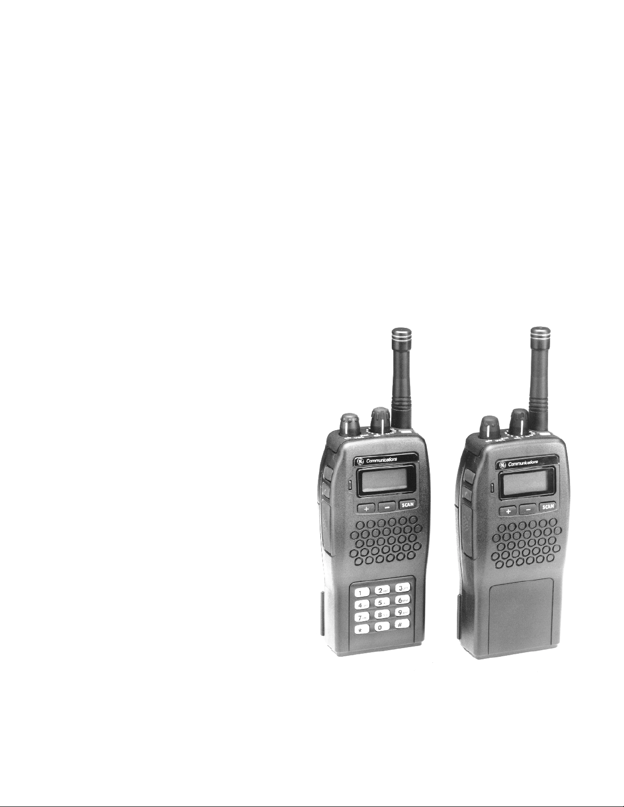
GENERAL
The KPC-300/400 Portable Radio Unit operates in the
conventional 403-512 MHz f requency band. The re are two
versions, Scan and System, with the System Version having
a DTMF keypad . Up to sixteen (16) RF chan nels may be
pre-programmed into the radio using a personal computer.
Power output on each channel can be programmed for either
high power (4 watts) or low power (1 watt). The power output
on each channel can be toggled between high or low depended upon the pre-programmed setting with High/Low
button on the left side panel.
Each radio is ca pa ble of oper ati on in 12 .5 kH z or 25 kHz
channel spacing systems. System deviation for 12.5 kHz
channel spacing is 2.5 k Hz and 5 kHz for 25 kHz channel
spacing.
AE/LZB 119 1906 R1A
Figure 2 - System Radio
Figure 1 - Scan Radio
The KPC-300 r adio contain s three (3) b uttons on t he front
panel. The KPC-400 contains three (3) buttons along with a
twelve (12) button DTMF pad on the front panel. The scan
function allows monitoring of any or all channels. Any
channel may be scanned with or without a priority level. One
channel can be programmed for Priority 1 (P1) and another
for Priority 2 (P2), with any or all remaining channels
programmed as non-priority channels (S). There is also
Emergency mode transmission capability. A LCD display
provides status displa y of t he radio funct i on s a long with the
display of the s ele cte d ch an ne l num be r.
The Universal Device Connector (UDC), located on the
side of the radio, provides connections for external audio
accessories. This connector also allows the radio system
personnel to connect pro grammin g equipme nt and prog ram
the per-channel an d overal l ra dio fea tur es .
Figure 3 - Back, Left And Top Panel Views
5
Page 6

AE/LZB 119 1906 R1A
CONTROLS
The radio cont rols con sist of an ON/OFF/V OLUME control, PTT button, MONITOR button, Channel Select switch,
EMERgency button and a High /Low button.
ON/OFF/VOLUME
PTT BUTTON
MONITOR
Turn s radio on an d off and adju sts
audio listening level.
When the radio is turned on, it
will resume operation at the last
operating state (channel, etc.) and
the power-up alert tones will be
sounded. Three (3) beeps indicate
the radio is in the normal (recei ve
mode); four (4) beeps indicates
the radio is s c an ni n g. The operating status of the radio will be displayed in the Liquid Crystal
Display (LCD) window.
Pressing the
side of the radio will key the radio
transmitter .
If the radio is not scanning, it will
transmit on the selected (displayed) channel. If the radio is
scanning when the
pressed, the radio may be programmed to transmit on the selected channel or on the current
receive scan channel if the
pressed during the scan hang
time.
If the selected channel is programmed with Type 99 Tone Decode enabled, pressing the
button will disable Typ e 99 Tone
Decode by switching the radio
from the Selective Call mode to
the Monitor mode. The
ton must be released and then
pressed a second time to key the
radio.
The Monitor button has several
functions. Its operation will vary
depending upon programming.
PTT
button on the
PTT
button is
PTT
PTT
PTT
but-
is
CHANNEL SELECT
EMERgency
H/L
S
+
-
DTMF Keypad
(KPC-400 only)
toggle ON or OFF (if it is programmed on the selected channel).
The Monitor button is also used to
reset the radio after a T y pe 99 call
is recei ved. Quic kly pres s and r elease the button to reset the radio
to receive the next Type 99 call.
A rotary switch permits selection
of channels. Rotating the switch
clockwise increases the channels
and counterclockwise decreases
the channe ls. The c hannel i s visible by looking at the channel
switch from the top or viewing
the LCD display.
Pressing f or at least one (1) sec ond will transmit the emergency
ANI code on the selected chan nel
or pre-progra mmed cha nn el.
Selects the transmit power output
by toggling from high-low or
low-high.
Three (3) buttons below the LCD
display are used to control a variety of operations when used alone
and to control scan operations
when used in conjunction with
the S button.
Toggles the scan feature on and
off.
Used in conjunction with the
button to add channels to the scan
list or increase the channel’s priority status.
Used in conjunction with the
button to erase the selected channel from the scan list.
Permits operator to make telephone interconnect calls on radio
systems equipped with this option.
S
S
When the Monitor button is
pressed and held down, all transmissions will be heard after three
(3) seconds have passed, even if
Channel Guard protected. This
permits channel monitoring before transmitting. If the button is
held for more than three (3) seconds, Channel Guard decode will
The top row of buttons (
2, 3
to three pre-programmed telephone interconnect numbers (see
Telephone Interconnect Calls
section).
) provide access to up
1,
6
Page 7

AE/LZB 119 1906 R1A
INDICATORS
The Liquid Crystal Display (LCD) indicates the channel
number. In addition there are seven (7) status indicators
(flags) which show scan status, Type 99 T one Decode status,
transmit High/Low power status and Channel Guard status.
The LCD backlighting will turn on anytime a control
button is pressed. It will remain on for five (5) se conds af ter
the button is released. If a control button is pressed while the
backlight is on, the backlight remains on for another five (5)
seconds. Backlighting may be programmed to remain o ff at
all times.
SCN HI
S P1 P2
PG CG
Figure 4 - Liquid Crystal Display (LCD)
CHANNEL
The selected channel number is
12
displayed in the LCD window..
When data is written into or read
from the radio a
P
is displayed.
when the selected channel is
placed in the monitor mode or the
reception of a call.
CG
HI
When this indicator is on, Channel Guard or digital Chanel Guard
is enabled on the select ed channel. The indicator will go out
when the selected channel is
placed in the monitor mode.
When this indicator is on, the selected channel is enabled for
transmit high power.
OPERATION
Detail operatin g procedures ar e found in Operator ’s Man-
ual AE/LZT 123 1898.
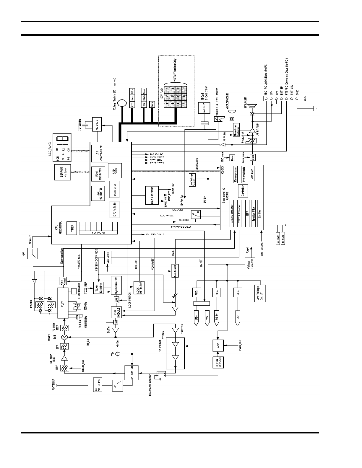
THEORY OF OPERATION
Refer to the Bl ock Diag ram durin g the following expla-
nations.
TRANSMITTER
STATUS
TX LED
SCN
S
P1
P2
PG
Red light on steady - transmitter
is active or keyed.
Red light blinking - low battery
voltage, recharge or replace battery.
Yellow on steady - channel busy
indication, radio has detected a
carrier on selected channel.
This status indicator turns on
when the scan function of the radio has been enabled.
When this indicator is on, the selected channel is a non-priority
scan channel.
When this indicator is on, the selected channel is a Priority 1 scan
channel.
When this indicator is on, the selected channel is a Priority 2 scan
channel.
When this indicator is on, the selected chan nel is prog rammed as
a paging channel (Type 99 Tone
Decode). The indicator will blink
The transmitter consists of an exciter Q201, PA module
U201, auto power control (APC) U202 with Q202 and Q203,
directional coupler Z201 and associated components. The
local signal input of approximately 0 dBm to the transmitter
is provided by the synthesizer to the exciter. An amplifier
provides 17 dB of gain to prod uce +17 dBm (50 mW) of driv e
level to the PA module. During the receive mode, a band
switch diode, D202, attenuates the rece i ve f irst loca l osc illator signal at the exciter input to reduce LO leakage at the
antenna connector. T he PA module is a 3-stage amplifier that
provides a minimum RF power output of 7.0 watts at a
battery voltage of 7.2 VDC. The RF power output is fed
through the directional coupler Z201 to the antenna. A
shottkey diode D201 converts the detected RF signal in the
directional coupler to a DC voltage to feed the auto power
control circuitry.
Low Pass Filter
The low pass filter Z101 and impedance matching network, consisting of L121 and C171 are provided to prevent
excessive transmitter harmonics during the transmit function.
Tx/Rx Antenna Switch
The Tx/Rx antenna switch, consisting of D101, D102 and
associated circuitry, provides the switching of RF output to
the antenna and the receive signal to the receiver . During the
receive function, the diodes are cut of f, isolating the tra nsmit
circuit from the antenna. During the transmit function, +5
volts is supplied to both diodes, turning them on and feeding
the RF output from the transmitter PA module through the
low pass filters via D101 to the antenna. The RF output is
suppressed at the receiver RF front end filter by D102.
7
Page 8
AE/LZB 119 1906 R1A
Figure 5 - Block Diagram
8
Page 9

AE/LZB 119 1906 R1A
Rf Power Control
The DC voltage detected by the directional coupler Z201
is supplied to comparator U202 where it is compared with
the power reference voltage PWR_REF. This comparison
voltage controls the bias voltage to the PA module by drive
transistor Q202, and the output power is stabilized by the
auto power control circuitry. PWR_REF is provided by the
central processing unit (CPU) from information programmed into the EEPROM. The PWR_REF voltage consists of six reference voltages: low frequency, middle
frequency an d h igh fr eque nc y b an d in bo th th e h igh an d low
power mode s. This po wer contro l provide s the flat ness of t he
RF output under varied temperature, voltage supply and
frequency bandwidth conditions.
RECEIVER
The receiver has a dual conversion circuitry consisting of
a receiver front end, RF amplif ier Q101, 1st mixer Q102, 1st
IF 70 MHz Monolithic Crystal Filter (MCF) Z102 and Z601,
IF amplifier/limiter/discriminator U101, 2nd IF 455 kHz
ceramic filters Z107, Z104, Z105 a nd c eram ic disc rim inator
Z106. Receiver IF selectivity for 25 or 12.5 kHz channel
spacing is determined by selecting the 455 kHz ceramic filter
Z104 for 25 kHz spa cing or Z10 5 fo r 12 .5 kHz spa cin g.
The demodulated receive audio at the AF OUT port o f
U101 is adjusted by Q104, R113 and R114 to produce a
constant demodulated audio level input into the Audio
Speech Pro cessor (ASP) regardless of th e receiver channel
spacing mode, 12.5 or 25 kHz. The receive audio gain controlled by Q104 , R113 and R114 is increased by 6 dB when
the receiver is switched from 25 kHz to 12.5 kHz channel
spacing. Received audio signals and beep tones are amplified
by audio frequency power amplifier U407 to achieve the
rated 0.5 W audio output power to speaker SP1.
remove the 1st IF image (F
MHz) and other out-of-band spurious responses. Total gain
is approximately 8 dB with the first IF image rejection more
than 68 dB.
To achieve the required RF bandpass filtering characteristics across the frequency band, the first front end filter
is electronically tuned by c hanges in the B AND_SW volta ge
which is fed to varactor diode D601-D603. This voltage is
generated by the D/A converter U421 from the CPU input.
The frequency band is divided into three sub-split bands, one
at the low end, one in the middle and one at the upper end of
the band. The CPU determines which sub-split the desired
receive frequency is in and provides the appropriate digital
input to U421 to generate the correct BAND_SW signal for
RF passband tuning.
The recei ve signal is applie d to dual gate GaAsFE T mixer
Q102 and mixed with the 0 dBm local oscillator injection
from the synthesizer section to produce the 70 MHz first IF
signal.
70 Hhz Filter
The mixer output is connected to the matching circuit and
provided to the four pole 70 MHz MCF Z102. The 70 MHz
crystal filter reduces the second IF image response (F
kHz) to meet spurious response specification. The output of
Z601 is applied to the 2nd mixer in the IF IC U101 through
the matching circuitry.
U101 consists of the second mixer, two IF amplifiers/limiters, a quadrature detector and a noise filter amplifie r.
The second mixer downconverts the first IF 70 MHz signal
to the second IF frequency of 455 kHz. Crystal resonator
Y101 and associated components provide a 69.545 MHz
second IF local oscillator signal. Y101 operated in the third
overtone mode.
-140 MHz) and 1st IF/2 (-35
rx
rx
-910
Short circuit protection for U407 consists of U416 and
Q416. When AF P A AMP outputs, SP+ and SP-, are shorted
together or shorted to ground, an excessive current will be
sourced through transistor Q407 which is the pass transistor
that provides bias to U407. This voltage drop across pass
transistor Q407 will be compared in differential amplifier
U416 and fed to voltage level translator Q416 which sends
the excessive current status sta te information to the CPU. The
CPU then sends a signal to Q407, turning it off and removing
bias from U407. The software in the CPU assumes the short
circuit is an intermittent short and resets for the excessive
current state approximately six (6) seconds later. If the excessive current state still exists, the CPU again turns Q407
off. After five retries, the CPU assumes the short circuit is
not intermittent and keeps Q407 turned off. The short circuit
condition must be removed before the radio is turned off and
then back on to reset the CPU.
Receiver Front End And Mixer
The receive signal is fed from the antenna to a bandpass
filter, a RF amplifier and an additional bandpass filter to
The second mixer output is applied to the 455 kHz ceramic filter Z107 and then to the first IF amplifier/limiter.
The first IF amplifier/limiter output is provide to either 455
kHz ceramic filter Z104 (for 25 kHz channel space mode) or
Z105 (for 12.5 kHz channel space mode). These filters are
switched by analog sw itches U102, U 103, U107 and U10 8
depending on th e desired channel spacing mo de. Ceramic
discrimina tor Z 106 and i nte rnal qua drat ure de tec tor pro vi de
the demodulated audio output signal at AF OUT. The demodulated audio signal, filtered with an internal low pass
filter (fc ≅47 kHz) is then routed to the baseband audio signal
processor U401 and a noise squelch circuit.
The noise squelch circuit consists of slow and fast squelch
time constants and an additional high pass filter (fc ≅4.0
kHz). The slo w squ elch tim e cons tant i s around 70 ms and is
provided to U40 4-2. The fas t squelch time c onstant is ar ound
8 ms and is p rovided t o U404-3. Dur ing scanni ng mode, only
the fast squelch is monitored by the CPU. In all other modes,
the slow squelch is monitored.
9
Page 10

AE/LZB 119 1906 R1A
Synthesizer
The synthesizer circuit generates all transmit and re ce ive
RF frequencies. This circuit consists of synthesizer IC U302,
temperature compensated crystal oscillator (TCXO) U303,
voltage controlled oscillator (VCO) U301 and associated
loop filter circuitry.
The VCO operates at the transmitter frequency during
transmit function and 70 MHz below the receive frequency
during the recei v e fu nction . The synt hesi zer is cont rolled by
the CPU. Frequency stability is maintained by the TCXO
module.
A portion of the VCO output is applied to the synthesizer
IC and divided by 65/64 dual modulus prescaler, which is
set by pulse swallow counter A and programmable counter
B to provide a 6.25 kHz output for comparison with a
reference signal. The reference signal is derived from the
12.8 MHz TCXO module. The synthesizer IC divides the
12.8 MHz signal down to the 6.25 kHz signal. (The KPC300/400 PC Programming Software will only permit synthesis of transmit or receive frequencies that are integer
multiples of 6.25 kHz. Other frequencies cannot be input
into the radio’s personality.) An unlock detector is used to
prevent transmission when the freq uency synthesizer is un locked.
Audio modulation from the Audio Signal Processor
(ASP) IC U401 is applied to the VCO modulation input via
amplifier U402 and the TCXO modulation input via amplifier U403. Th e g ai n of U402 is adjusted de pendent upon the
channel spacing mode of the radio. In the 25 kHz channel
space mode, U418 is open-circuited, removing R453 from
being in parallel with R411. In the 12.5 kHz channel space
mode, U418 is short-circuited, placing R453 in parallel with
R411 and reducing the transmitter audio gain by a factor of
two. (This esta blish es t he 5 kHz ma xim um fr eque nc y d e viation for 25 kHz chan nel spacin g and the 2. 5 kHz maximu m
frequency deviation for 12.5 kHz channel spacing.) VR403
and VR402 are adjustable to provide a constant modulation
flatness for voice audio and Channel Guard (CG) and Digital
Channel Guard (DCG) sub-audible mo dulation.
MOSFET transistor Q316 is turned on during the transmit
mode to change the loop gain in order to get lower modulation frequency response. A ripple filter, consisting of Q312,
C312 and R331, provides a filtered 4.7 VDC to the VCO to
improve the p hase noise characteri stic of the rece iver local
injection signal for enhanced receiver pe rf or mance for adjacent channel selectivity, intermodulation and FM hum and
noise.
Audio Logic
The audio logic se ction consists of CPU U404, Audio
Signal Processor (ASP) IC U401, EEPROM U406 and associated components. The CPU controls all radio operations.
The EEPROM contains the personality data and the alignment data.
CPU
The CPU contains the LCD controller, LED controls, 32k
bytes of R OM, 1k byte of RAM, a n 8-chann el A/D con v erter
and a 2-channel D/A converter. The CPU generates DTMF
tones, alert tones, beep tones, GE-STAR (ANI) codes and
Digital Channel Guard (DCG) encode codewords. The DCG
encode codeword from the CPU is applied to a low pass filter
in the ASP IC U401 and summed with the voice signal at
U402. Received DCG codewords and T ype 99 tones from the
ASP U401 are supplied an d deco ded by the CPU .
AUDIO SIGNAL PROCESSOR U401
The ASP IC U401 contains the CG encoder and decoder,
pre-emphasis audio shaping filters, de-emphasis audio shaping filters, limiter, post-limiter filter (i.e., splatter filter) and
various Switched Capacitor Filters (SCF). U401 generates
CG tones controlled by the CPU. CG and DCG sub-audible
modulation signals are summed with the voice audio signal
at op-amp U402 and supplied to the VCO and TCXO modulation inputs.
The demodulated audio signal from IF IC U101 can
provide voice signal information, CG tones, DCG codewords
and Type 99 two-tone sequential information. CG tones are
filtered by a tone filter and decoded in the ASP. DCG codewords are filtered by the tone filter and input to multiplexer
U417. T ype 99 tones are filtered by a bandpass filter and also
input to U417. Multiplexer U417 selects either the DCG or
Type 99 signals, outputs the signal to a comparator to
“square” the signal to a TTL level digital w ave form and then
sends the digitized signal to the CPU for detection.
Before the transmit voice audio signal is input to the ASP ,
it can be optionally mixed with DTMF or GE-STAR (ANI)
encode signals. These ba seband signa ls are p re-empha sized,
bandpass filtered, hard limited, run through a post-limiter
filter (splatter filte r) a nd then summed at op-a mp U402 with
CG tones or DCG codewords.
CLOCK SHIFT
The CPU uses a n ominal 7.3728 MH z clock frequency,
which is divided down to 3.6864 MHz to become the clock
frequency input provided to the ASP IC U401. Harmonics of
this clock frequency can potentially interfere with the performance of the transmitter and receiver , producing self-quieting “beat” notes at specific receiver frequencies or
producing an audio whine at specific transmitter frequencies.
A clock shift can be programmed for each channel’s receive
and/or transmit frequency to move the potentially interfering
harmonics of the micr oprocessor cl ock frequency. The microprocessor clock frequenc y is shifted more than +100 ppm,
effectively moving potentially interfering clock harmonics
off-channel.
10
Page 11

AE/LZB 119 1906 R1A
POWER SUPPLY
The battery voltage, provided by six nickel cadmium
cells, is a nominal 7.5 volts. This voltage is provided to the
series regulators via a 4 amp fuse F401. The regulated supply
provides +5 volts for the logic section, the analog section,
receiver and transmitter sections. The +5.5 v olts f or the PLL
frequency synthesizer section is also provided.
RADIO PROGRAMMING
PC PROGRAMMING
The KPC-300/400 Portable Radio is programmed using
an IBM compatible personal computer equipped with a RS232 serial port. Adapter TQ-3370 pro vides the RS-232 se rial
interface an d the cable between the PC and the adapter box.
Programming Cabl e RPM 113 24 72/1 pr ovides the conn ection from the adapter box to the radio’s Universal Device
Connector (UDC). The programming software is AE/LZY
213 761.
PROGRAMMABLE FEATURES
The following features are programmable on a per-channel basis:
• Receive Frequency
• Transmit Frequency
• Channel Busy Lock-Out
• Carrier Control Timer (CCT)
• Squelch Tail Elimination (STE)
• Fixed Priority 1 Scan Channel
• Channel Guard Encode/Decode (Tone or Digital)
• Type 99 Tone Decode
• Autom atic Number Identification (ANI)
• Telephone Interconnect DTMF Keypad Enable
(KPC-400 only)
The following fe atures are pr ogrammable on an ov erall radio
basis:
• Display B acklighting
• Alert Tones
• Eme rgency Chan ne l
• Three (3) Auto-Dial T elephone Numb ers (KPC-400
only)
CHANNEL BUSY LOCK-OUT
If channel busy lock-out has been programmed on the
selected channel, the transmit function will be inhibited
when the op erator presses t he PTT button while the radio
detects a carrier on the channel unless the carrier is modulated with the corresponding Channel Guard tone or code for
that selected channel. The radio will immediately begin
transmitting when the carrier disappears. Channel bu sy lockout continues to function if Channel Guard decode is disabled with the MONITOR button. The ch annel-busy feature
is programmable on a per-channel basis. Type 99 cannot be
programmed on a channel with channel busy lock-out.
CHANNEL GUARD
Channel Guard (CG) provides a means of restricting calls
to specific radios through the use of Continuous T one Coded
Squelch System (CTCSS) tone frequencies ranging from
67.0 Hz to 210.7 Hz. Digital Channel Guard (DCG) also can
provide a means of restricting calls through the use of 83
standard Continuous Digital Coded Squelch System
(CDCSS) cod es. Each chan nel may be p rogram med for en code/decode, encode only, decode only or for no CG or DCG.
Both tone frequencies and digital codes may be used. The
tones and codes are listed in Tables 1 and 2.
SQUELCH TAIL ELIMINATION (STE)
STE is used with tone and Digital Channel Guard to
eliminate squelch tails. The STE burst is transmitted when
the microphone PTT is released. The receiving radio decodes
the burst and mutes the recei ver audio for 250 ms. T his mute
time allows the transmission to end and to eliminate the
squelch tail. The radio looks for STE on the received signal
when the micropho ne is either on or off-hook. S TE is enabled
for transmit and/or rece ive through PC prog ra mming .
AUTOMATIC NUMBER IDENTIFICATION
(ANI)
Automatic Number Identification is a 320 ms burst of
code (GE-STAR) that is generated at the beginning of each
transmission to identify the radio unit to the dispatcher. If
programmed, a beep is sounded at the end of ANI transmission to indicate when conversation can begin as the microphone is disabled until the ANI transmission is completed.
Systems with CG require that ANI be delayed long
enough for the syste m to respond before ANI can be decoded.
A programmable delay is provided to meet this requireme nt.
For exampl e, a del ay of 350 m s re quire s t he op erat or to wai t
for 670 ms after pressing the PTT before conversation can be
started. If desired, th e ANI messag e can be progra mmed to
be sent at the end of a transmission.
11
Page 12
AE/LZB 119 1906 R1A
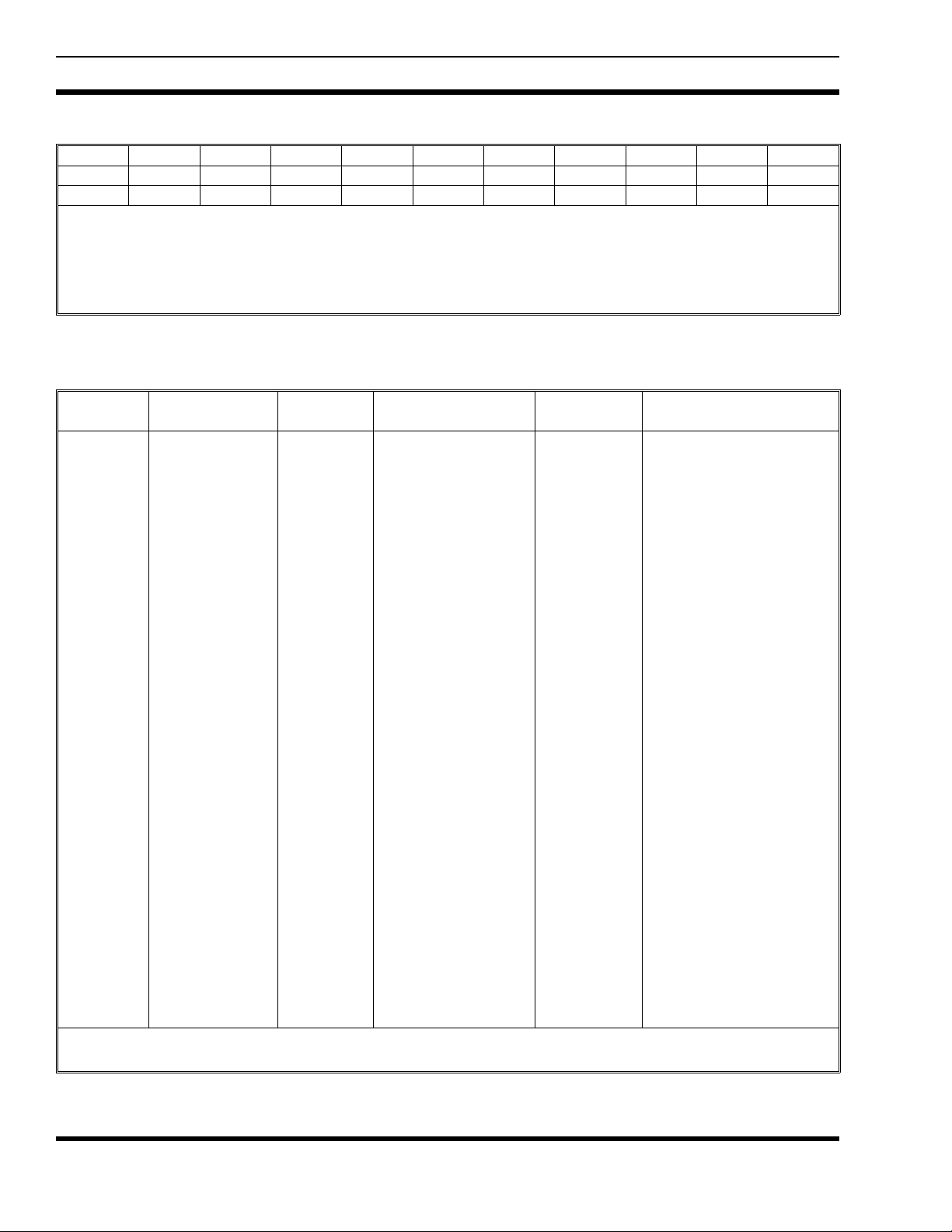
Table 1 - Standard Tone Frequencies (Hz)
67.0 71.9 74.4 77.0 79.7 82.5 85.4 88.5 91.5 94.8 97.4
100.0 103.5 107.2 110.9 114.8 118.8 123.0 127.3 131.8 136.5 141.3
146.2 151.4 156.7 162.2 167.9 173.8 179.9 186.2 192.8 203.5 210.7
1. Do not use 179.9 Hz or 118.8 Hz in areas served by 60 Hz power distribution systems (or 100.0 Hz or 151.4 Hz in areas supplied with 50 Hz power).
Hum modulation of co-channel stations may "false" Channel Guard decoders.
2. Do not use adjacent Channel Guard tone frequencies in systems employing multiple Channel Guard tones. Avoid same-areas co-channel use of
adjacent Channel Guard tones whenever possible. As stated in TIA/EIA-603, there is a possibility of decoder falsing.
3. To minimize receiver turn-on time delay, especially in system using Channel Guard repeaters or receiver voting, choose the highest usable Channel
Guard tone frequency. Do not use tones below 100 Hz when it is necessary to meet the receiver response time requirements as specified in
TIA/EIA-603.
Table 2 - Digital Channel Guard Codes
PRIMARY
CODE
023
025
026
031
032
043
047
051
054
065
071
072
073
074
114
115
116
125
131
132
134
143
152
155
156
162
165
172
174
205
223
226
243
244
245
EQUIVALENT
CODE
340 766
566
374 643
355
375 707
520 771
405 675
301
603 717 746
470 701
640
360 721
327 615
534 674
060 737
173
572 702
605 634 714
273
333
366 415
233 660
517 741
416 553
354
057
142 270
135 610
350 475 750
104 557
267 342
176 417
370 554
PRIMARY
CODE
251
261
263
265
271
306
311
315
331
343
346
351
364
365
371
411
412
413
423
431
432
445
464
465
466
503
506
516
532
546
606
612
624
627
631
NOTE:
Primary codes in bold are unique Ericsson codes.
EQUIVALENT
CODE
236 704 742
227 567
213 736
171 426
427 510 762
147 303 761
330 456 561
321 673
372 507
324 570
616 635 724
353 435
130 641
107
217 453 530
117 756
127 441 711
133 620
234 563 621 713
262 316 730
276 326
222 457 575
237 642 772
056 656
144 666
157 322
224 313 574
067 720
161 345
317 614 751
153 630
254 314 706
075 501
037 560
231 504 636 745
PRIMARY
CODE
632
565
654
662
664
703
712
723
731
732
734
743
754
036
053
122
145
212
225
246
252
255
266
274
325
332
356
446
452
454
455
462
523
526
EQUIVALENT
CODE
123 657
307 362
163 460 607
363 436 443 444
344 471 715
150 256
136 502
235 611 671
447 473 474 744
164 207
066
312 515 663
076 203
137
535
525
253
536
542 653
661
425
655
652
550 626
433 552
521
467 511 672
524 765
513 545 564
533 551
472 623 725
647 726
562 645
12
Page 13

AE/LZB 119 1906 R1A
CARRIER CONTROL TIMER
This feature, programmable on a per-channel basis, prevents unnecessary channel traffic and radio damage if the
transmit timer limit is exceeded. If the programmed timer
times-out during a transmission, the radio will beep and stop
transmitting. The beeping tone will continue until the operator releases the PTT button. Releasing the PTT button resets
the timer.
TYPE 99 TONE DECODE
The radio is programmable to power-up in either selective
(Type 99) or monitor mode for channels programmed for
Type 99 decode.
When select ive mode is chosen, t he radio opera tes as a
tone and voice receiver and allows only those calls that are
tone coded for the radio to be heard. Selecting monitor mode
allows all calls with the correct Channel Guard (if programmed) on the channel to be heard.
In either mo de, when a c orrect T99 and Chann el Guard
(if programmed and enabled) have been decoded, a series of
intermittent beeps will be heard to alert the operator of an
incoming call. The PG status flag will blink in the display to
indicate that a call has been received. If the selective mode
was chosen, the radio switches automatically to monitor
mode.
At the end of the message, if selective mode is desired,
press and release the MO NIT OR button to reset the Type 99
tone signalling function. The PG status flag will cease blinking.
While in selective mode, the radio can be put in monitor
mode by pressing and releasing the PTT. A series of beeps
is sounded whle the PTT is pressed to indicate that no
transmission has occured and the monitor mode has been
selected as indicated by with the blinking of the PG status
flag. A second press of the PTT will result in normal
transmission.
The radio is programmable to decode any Ericsson or
Motorola decode combinations from any one of two T99 tone
tables on a per-channel basis. T ransmit and/or r ecei ve Channel Guard can be programmed to any channel with Type 99.
Type 99 receive Channel Guard (if programmed) can be
disabled by pressing the MONITOR button for more than
three (3) seconds.
NOTE
Resetting Type 99 from monitor to selective mode does not
affect Channel Guard switch setting.
If a T ype 99 channel is in the scan list and scan is enabled,
Type 99 tones are ignored. Scan nin g is pr ov ide d o n a ca rr ier
and Channel Guard basis only.
TELEPHONE INTERCONNECT (DTMF)
(KPC-400 ONLY)
The operator may make telephone interconnection calls
on radio systems equipped for this option. Specific procedures for placing these calls are determined by the ope rating
system.
There are two methods to make telephone interconnect
calls. One method uses the top three keys (
to send one of three pre-programmed numbers. The other
method is to use the keypad (
the telephone number.
The keypad is not active until the PTT button is pressed.
Therefore, the PTT button must be pressed at all times when
operating any button on the DTMF keypad. Communications
takes place in a simplex mode. You cann ot talk and listen at
the same time. The PTT button must be pressed each time
you wish to talk and, released when you wish to listen.
0-9
1,2,3
) to manually enter
SCAN
The scan feature permits monitoring of up to 16 receive
channels. The scanne d channe ls can b e any freque ncy wi thin
the frequency ba nd limits of the rad io and can be Chann el
Guard protected (tone or dig ital).
Any channel can be scanned with or without a priority
level. One channel can be programmed for Priority 1 (P1),
another for Priority 2 (P2) or any or all remaining channels
programmed as Non-Priority (S). The radio can be pre-programmed to permit an operator front panel selectable scan
list, a fixed Priority 1 channel or a selected Priority 1 channel
using the channel select switch.
Scan Vocabulary
The following terms are frequently used in scan operation
descriptio n.
• Simple Scan - describes the condition when scan is
enabled and there i s no activity on any ch annel in
the scan list.
• Priority Scan - describes the condition when scan is
enabled and the priority scan channel is sampled
during the scanning of the channels on the scan list.
• Channel Guard Scan - describes the condition when
scan is enabled and tone or digital Channel Guard
must also be detected before locking on any channel.
• Selected Channel - indicates that this is the last
channel that the operator selected with the channel
select switch. This channel is displayed unless sca n
is enabled and activity is detected on another channel being scanned.
)
13
Page 14

AE/LZB 119 1906 R1A
• Receive Channel - indicates the channel that has
been detected and identified with the correct c arrier
and Channe l G ua rd (i f en ab led ). Th e r eceive cha nnel number will be shown in the display.
• Scan List - indicates an internal list either pre-pro-
grammed or pro gr amme d fr om th e fr on t p anel that
includes each channel status that will be scanned
when the scan mode is enabled.
• Non-Scan Channel - indicates a channel that is not
in the scan list and will not be scanned when scan
is enabled.
• Non-Priority Channel - indicates that this channel
is on the scan list. Activity on this channel will be
interrupted by activity on either the Priority 1 or
Priority 2 channel.
• Priority 2 Channel - indicates that this channel is
also on the scan list. Activity on this channel will
interrupt any activity on any non-priority channel.
However, activity on this channel will be interrupted only by activity on the Priority 1 channel (if
on scan list).
• Priority 1 Channel - indicates that this channel is
also on the scan list. Activity on this channel will
interrupt and supercede any other channel activity.
• Channel Activity - indicates the presence of a cor-
rect carrier with correct Channel Guard (if programmed).
• Ha ng Time - describes the time i nterval (pre-pro-
grammable) that a channel remains locked to a
frequency although no ch annel activity is present.
This condition arises after channel activity has
stopped or the PTT button has been released.
• Fixed Priority 1 Channel - indicates that the channel
has been pre-programmed as the Priority 1 scan
channel and cannot be ch anged by the operator.
• Selected Priority 1 Channel - indicates that the
channel selected by the channel select switch will
be the Priority 1 scan channel. The operator can still
select the Non-Priority and Priority 2 channels.
Pre-Scan Operation
A scan list must be created before scan operation can be
used. The scan list can be created in several ways. The ra dio
will not go into the scan mode when no channel are programmed or in a scan list.
• Fixed Programmable - the scan list is pre-pro-
grammed using the PC programming softwaare and
cannot be changed by the operator.
• Front Panel Programmable - the scan list is created
by the operator using the front pa nel cont rols.
• Selected Channel Programmable - the operato r cr e-
ates the scan list for all Non-Priority and Priority 2
channels. The Priority 1 channel is selected by the
channel select switch. This is also pre-programmable using the PC programming software.
ALERT TONES
Alert tones or “beeps” are sounded when a button is
pressed and w hen the oper atin g stat us of t he rad io chan ges.
All alert tones may be programmed to be remain off.
Power-up Self-test
Each time the radio is turned on, it will perform power-up
self-test. All display segments will turn on, and after succ essful completion of the test, the radio will change to the last
operating state (channel, etc.) and sound three (3) or four (4)
beeps. Three (3) beeps sound if the radio is operating in the
normal (not scan) state. Four (4) beeps will sound if the radio
is scanning. The status will be indicated in the LCD. If the
radio fails the self-test, no beeps will be sounded.
Carrier Control Timer
This feature, programmable on a per-channel basis, prevents unnecessary channel traffic and radio damage if the
transmit timer limit is exceeded. If the programmed timer
times-out during a transmission, the radio will beep and stop
transmitting. The beeping tone will continue until the operator releases the PTT button. Releasing the PTT button resets
the timer.
Channel Busy Lock-out
If channel busy lock-out has been programmed on the
selected channel, the transmit function will be inhibited
when the op erator presses t he PTT button while the radio
detects a carrier on the channel unless the carrier is modulated with the corresponding Channel Guard tone or code for
that selected channel. The radio will immediately begin
transmitting when the carrier disappears. Channel bu sy lockout continues to function if Channel Guard decode is disabled with the MONITOR button. The ch annel-busy feature
is programmable on a per-chan ne l basis.
Type 99 Alert Tone
The Type 99 alert tone, indicating a receive Type 99 call,
may be enabled or disabled by programming. If the programmed tone sequence is detected, the radio will beep two
(2) times. If the alert tone is disabled, no alert tone will be
present when a Type 99 call is received.
ANI Alert Tone
The Automatic Number Identification (ANI) alert tone
beep can be enabled or disabled by programming. If the alert
tone is enabled, a beep will sound after the PTT is pressed
to indicate to the operator to begin voice transmission. Some
communication systems require a time delay before voice
transmission begins. If the alert tone is disabled, no bee p will
sound.
SCAN Alert Tone
The radio will sound a beep when the
pressed.
S
button is
14
Page 15

AE/LZB 119 1906 R1A
Priority-One (P1) Scan
If the Priority 1 alert tone is enabled by programming and
the radio r eceives a signal on th e Priority 1 chan nel when
scanning, the radio will sound a beep.
Radio/Channel Failure
The simultaneous flashing of the LCD display and the
sounding of beeps indicates the synthesizer is unable to
correctly lock on the selected channel. At this time the radio
changes to a mute condition and no audio is heard from the
speaker when receiving and the transmit is inhibited if the
PTT button is pressed. Select another channel, change the
battery pack or have the radio repaired.
SCAN OPERATING MODES
Simple SCAN
Once SCAN is activate d, the ra dio will perform a Sim ple
SCAN routine. This routine is performed when there is no
activity on any of the channels that are in the Scan list.
The scanning list at right,
is an example of the routine performed when there
are more than four (4)
channels in the Scan list.
(The abbreviation "np" indic ates a non-prior ity channel,
and P1 and P2 indicate Priority 1 and Priority 2, respectively.)
The scanning list at right,
is an example of the routine performed when there
are less than four (4) channels in the Scan list.
The above scanning orders assume that Priority 1 and
Priority 2 channels exist. If they have not been assigned,
their positions in the scanning order are eliminated.
np6...np5...np4...np3...P1..
.P2...np2...np1...np6...np5.
..P1...P2...np4...np3...np2..
.np1...P1... P2 , et c.
np3...np2...np1...P1...P2...n
p3...np2...np1...P1...P2,
etc.
NOTE
Priority channels will continue being scanned during hang
time.
PTT Pressing the PTT switch causes the ra-
dio to transmit on the selected channel
frequency an d to stop the sc anning routine. A programmable hang time (0.3
to 5.0 seconds) will start as soon as the
PTT switch is released. Scanning will
resume at the end of the hang time. The
hang time is a PC prog rammable option
and can be enabled or disabled.
Channel Change Any channel change will change the
selected channel and show it in the
display window. A channel change
will also stop the scanning routine for
a fixed, 2-second hang time. If no activity is detected on this new selected
channel during this 2-second hang
time, scanning will resume.
Priority SCAN
As soon as any activity is detected on a channe l, the radio
will change the scanning mode from Simple SCAN to Priority SCAN. The new receive channel will appe ar in the LCD
window.
If the receive channel is a
Non-Priority channel,
both Priority 1 and Priority 2 channels will be sampled (scanned) every 500
milli-seconds in the order
indicated at the right.
• If a Priority 1 channel has not been established, the
radio will only break away to sample the Priority 2
channel every 1.0 second.
• If a Priority 1 channel has been established but not
a Priority 2 channel, the radio will break away to
sample the Priority 1 channel every 500 milliseconds.
• If neither a Priority 1 or Priority 2 channel has been
established, the radio will lock on this channel until
activity on this channel goes away.
• When the receive channel is a Priority 2 channel,
the radio only samples Priority 1 channel every 500
milliseconds.
• When the receive channel is a Priority 1 channel, no
other channels will be scanned.
P1...P1...P2...P1...P1...P2..
.P1...P1...P2, etc.
15
Page 16

AE/LZB 119 1906 R1A
Once activity on t he receive channel has ended, a programmable hang time (0.3 to 5.0 seconds) is started. Scanning will resume at the end of the hang time if there is no
activity on that channel. The selected channel will appear
now on the display . Note that Priority channels will continue
being scanned during hang time.
To alert the operator of an incoming call on the Priority 1
channel, an option is available to sound a beep upon receiving this Priority 1 channel.
Scanning for Channel Guard
The scanning for Channel Guard option may be selected
if, in addition to carrier activity alone, a correct Channel
Guard is also required to lock on a channel when scanning.
This option is selected on an individual radio basis.
Scanning Priority channels with the wrong Channel
Guard will change the scanning rate as follows:
Priority 1 with wrong Channel Guard: The radio
will change its Priority 1 sample rate from 0.5
seconds (.5 seconds) to 2.5 seconds, but it will
still sample the Priority 2 channel every 1.0
second.
Priority 2 with wrong Channel guard: The radio
will change its Priority 2 sample rate from 1.0
second to 5.0 seconds, but will continue to sample the Priority 1 channel every 500 milliseconds (.5 seconds).
PTT The operator has two PC programma-
ble options to select from in regard to
what channel to transmit on. The operator can choose to transmit on the
selected channel or on the receive
channel. The transmit channel will be
shown on the display. Releasing the
PTT switch will unkey the transmitter
and start the programmable hang time
(0.3 to 5.0 seconds), if enabled. Scanning will resume again at the end of the
hang time unless there is activity on
that channe l.
TONE PROGRAMMING
An IBM-compatible person al computer using MS-DOS
and a Programmer Interface Box plus the proper programming software is used to program the T ype 99 tones, Channel
Guard tones, and Ch annel Guard digi tal code. Th e Programmer Interface Box is connected between the UDC on the side
of the radio an d th e b a c k of the perso na l c om pu t er. Refer to
Programming Guide for details.
Two sets of Type 99 tones can be programmed in the
radio. Any chan nel can be p rogramme d to decode any call
or all calls ba sed on an y one of the two tone sets . Indi vidual ,
group, and super group paging can be used. Motorola formats are also acc ep t ab le.
PG is displayed on the LCD when that channel has been
programmed to receive Type 99 calls. Both receive and
transmit Channel Guard may also be programmed to any
channel with Type 99 tone.
An Intermittent beep is sounded to alert the operator of
an incoming Type 99 call.
Upon receiving a call, the radio will open the audio and
flash the PG indicator until it is reset by momentarily pressing the MONITOR button.
NOTE
If a Type 99 channel is in the Scan list and SCAN is enabled,
Type 99 tones are ignored. Scanning is done on a Carrier
and Channel Guard basis only.
The optional Type 99 programming provides individual,
group, and super group call decode. The Motorola-formatted, two-tone, sequential signalling schemes can also be
decoded.
In Type 99 tone systems, calls will not be heard from the
receiver until the proper two tones are detected. When the
second ton e is decoded an d recognized as correct, an ale rt
tone sounds during the remaining portion of the second tone.
The receiver audio path opens and remains open to receive
messages until the decoder is reset. The PG indicator will
also flash to show a call has been received.
Channel Change Any channel change will change the
selected channel. The receive channel,
if any, will stop being displayed/heard
and replaced by the new selected channel. The scanning routine is temporarily stopped for a fixed 2 seco nds and
will resume again if there is no activity
on the selected channel.
NOTE
Priority channels will continue being scanned during hang
time.
16
The radio can be programmed with up to two separate
tables of tones. Either the Ericsson Type 99 format or the
Motorola format can be assigned to each tone table. The tone
decoder (individual, group, and super group for Ericsson
format or individual, group, and quick call for the Motorola
format) can be enabled individually for each channel. Once
enabled, one of the two tone tables can be selected for each
channel.
The Group Call format allows communication with all
radios in a group. Th e Supe r Grou p Call (in E ricsson Tone
systems) or Quick Call (in Motorola tone systems) allows
communications between all radios in a system.
Page 17

AE/LZB 119 1906 R1A
TYPE 99 FORMAT
Tone frequencies in the Ericsson tone system fall within
the range of 517.5 to 997.5 Hz.
In the tone format, the first tone can be f rom Tone Group
A (for individual or group calls) or from Tone Group C (for
super group calls). The second tone may be from Tone
Group B (for individual calls) or from Tone Group D (for
group or super group calls). The tone format is illustrated as
follows.
INDIVIDUAL
CALL
FORMA T
GROUP
CALL
FORMAT
SUPER
GROUP
CALL
FORMAT
For example, assume the paging number to be 123; the
first digit of the paging number is a "1." Look in Table 3 and
read down the column labeled "100’s Digit" to a "1." Read
horizontally across the column labeled "10’s Digit." The
Tone Group is B. The second digit of the pa gin g numb er is
a "2." The tone number is B2. Look in Table 4 and down
the column labeled "Tone Designator" to find B2. Read
horizontally across the column labeled "Tone Frequency."
The first tone frequency is 787. 5 Hz.
To determine the second tone frequency, look in Table 3
and, as before, find the first digit of the paging number ("1").
The second Tone Group is A. The thir d digit of th e paging
number is a "3" and the Tone Designator is A3. In Table 4,
read down the column labeled "Tone Designator" and find
A3. Read horizontally across the column labeled "Tone
Frequency." The second tone frequency is 802.5 Hz.
<...1.0 SEC...>
20%
TONE A
<...1.0 SEC...>
20%
TONE A
<...1.0 SEC...>
20%
TONE C
<...200 MS...>
25%
GAP
<...200 MS...>
25%
GAP
<...200 MS...>
25%
GAP
<..1.0 SEC..>
+300%,-0%
TONE B
<..1.0 SEC..>
+300%, -0%
TONE D
<..1.0 SEC..>
+300%, -0%
TONE D
Ta ble 3 - Ericsson Tone Groups
100’s
Digit
0
1
2
3
4
5
6
7
8
9
10’s
Digit
For First
Tone
A
B
B
A
C
C
C
A
B
NOT USED
1’s
Digit
For Second
Tone
A
A
B
B
C
A
B
C
C
MOTOROLA FORMAT
Tone frequencies in the Motorola tone system are within
the range of 288.5 to 1433.4 Hz. In the Motorola tone
format, the first tone may be one of three tones: A for
Individual Call, B for Quick Call, and C for Group Call. The
second or final tone is B in all cases.
NOTE
The radio is able to recognize the A, B, and C tones.
Individual, Group, and Quick Call formats may be used
simultaneously.
The Motorola tone format is illustrated as follows:
INDIVIDUAL
CALL
FORMAT
GROUP
CALL
FORMAT
QUICK
CALL
FORMAT
<..1.0 SEC..>
(Minimum)
TONE A
<..1.0 SEC..>
(Minimum)
TONE C
<..............................8 SEC..............................>
<..NONE..>
(Minimum)
GAP
<..NONE..>
(Minimum)
GAP
TONE B
<..3.0 SEC..>
TONE B
<.
.3.0 SEC..>
TONE B
For different paging numbers, locate the first digit in the
"100’s Digit" column and determine the tone frequencies as
described in the example.
Tone D is the diagonal tone used (in Ericsson systems
only) when the first and second tone frequencies are the
same. The standard frequency f or Tone D is 742.5 Hz, but
may be programmed with any tone frequency.
Individual Call
Tables 5 and 7 may also be used to determine the tone
frequencies. The first digit of the code determines the tone
group used in the code (see Table 5). Then Table 6 is used
to determine the actual tone frequencies. For a code of 124,
the tone groups used a re sho w n in Table 5. Tone A and T o ne
B are both located in Tone Group 1 and Tone B is tone
number 4. Refer to the following examples for additional
information.
17
Page 18

AE/LZB 119 1906 R1A
Example 1 - Code 098:
The digit "0" in Table 5 (First Digit of Code) shows the
Tone A is in Tone Group 4 and Tone B is in Tone Group 2
(see Table 5).
Tone number 9 in Tone Group 4 is 524.6 Hz.
Tone number 8 in Tone Group 2 is 879.0 Hz.
Example 2 - Code 265:
The digit "2" in T able 5 shows that both Tone A and T one
B are in Tone Group 2.
Tone number 6 in Tone Group 2 is 788.5 Hz.
Tone number 5 in Tone Group 2 is 746.8 Hz.
Group Call (Quick Call Format)
In Group Call applications, the tone group is determined
by Table 7, while the frequency is d etermined by Table 6.
Refer to the following examples.
Example 1- Group Call Code 07 (also code 27 and 37):
The digit "0" in Table 7 shows that Tone B is in Tone
Group 2 along with 20 to 29 and 30 to 39 . Tone number 7
in Tone Group 2 is 832.5 Hz (see Table 6).
NOTE
Group Call code numbers range from 00 to 99. However,
there are several Group Calls with the same Tone B
frequency. This limits the total number of Group Calls to
40.
Example 2 - Group Call 98 (also 48 and 88):
Ta ble 4 - Ericsson Tone Generator Frequencies
TONE
GROUP
AA0
BB0
CC0
DIAGONAL TONE 742.5
TONE
DESIGNATOR
A1
A2
A3
A4
A5
A6
A7
A8
A9
B1
B2
B3
B4
B5
B6
B7
B8
B9
C1
C2
C3
C4
C5
C6
C7
C8
C9
TONE
FREQUENCY
(Hz)
682.5
592.5
757.5
802.5
847.5
892.5
937.5
547.5
727.5
637.5
652.5
607.5
787.5
832.5
877.5
922.5
967.5
517.5
562.5
697.5
667.5
712.5
772.5
817.5
862.5
907.5
952.5
532.5
577.5
622.5
The digit "9" in Table 7 shows that Tone B is in Tone
Group 4 along with 40 to 49 and 80 to 89 . Tone number 8
in Tone Group 4 is 496 .8 Hz.
18
Page 19

AE/LZB 119 1906 R1A
Ta ble 5 - Motorola Type Code Numbers
First Digit
of
Code
1
2
3
4
5
6
7
8
9
0
A
Tone Group from
which T one A
is Selected
1
2
1
4
5
2
4
5
2
4
3
Tone Group from
Ta ble 6 - Motorola Type Code Numbers
TONE
NO.
1
2
3
4
5
6
7
8
9
0
TONE
GROUP 1
(Hz)
349.0
368.5
389.0
410.8
433.7
457.9
483.5
510.5
539.0
330.5
TONE
GROUP 2
600.9
634.5
669.9
707.3
746.8
788.5
832.5
879.0
928.1
569.1
which Tone B
is Selected
1
2
2
4
5
1
5
4
4
2
3
(Hz)
TONE
GROUP 3
(Hz)
288.5
296.5
304.7
313.0
953.7
979.9
1006.9
1034.7
1063.2
1092.4
Table 7 - Motorola Group Call Tone Groups (TG)
GROUP CALL
CODE NUMBER
00-09
10-19
20-29
30-39
40-49
50-59
60-69
70-79
80-89
90-99
TONE
GROUP 4
(Hz)
339.6
358.6
378.6
399.8
422.1
445.7
470.5
496.8
524.6
321.7
GROUP 5
TONE
(Hz)
584.8
617.4
651.9
688.3
726.8
767.4
810.2
855.5
903.2
553.9
TONE GROUP
(TONE B)
TG2
TG1
TG2
TG2
TG4
TG5
TG1
TG5
TG4
TG4
TONE
GROUP 6
(Hz)
1153.4
1185.2
1217.8
1251.4
1285.8
1321.2
1357.6
1395.0
1433.4
1122.5
19
Page 20

AE/LZB 119 1906 R1A
ALIGNMENT
This section describes the alignment procedure for the
radio. This procedure should be used whenever a board or
component is replaced or the operation of the radio is in
doubt.. Almost all alignment and checks can be accomplished through the Universal Device Connector (UDC) using the maintenance section of the PC Programming
Software. The setting of the transmitter deviation requires
the removal of the front case of the radio to adjust VR402
and/or VR403.
TEST EQUIPMENT
The following test equipment is recommended for radio
alignment:
• Communications Monitor (HP8920B or equi valent )
• DC Voltmeter (1 megohm input impedance)
• DC Power Supply (7.5 volts at 5 a mp)
• IBM or compatible person al comp ute r
• PC Programming Software
• Programming Adapter Box TQ-3370 with Interface
Cable
• Rad io Progr amming Ca ble
• DC Power Adapter
• DC Power Cable
• RF Coaxial Cable (50 ohms)
Initial Setup
CPU Clock Adjustm en t C 445
1. Set communications monitor for Antenna Input mode.
2. Ensure that CPU clock shift is turned off for receive.
3. Monitor on Communications Monitor the 7.3728
MHz radiation leakage using any type of antenna.
4. Adjust trimer capacitor C445 to obtain 7.3728 MHz
50 Hz.
5. Enable CPU clock shift and con firm that clock shifts
approximately +800 Hz.
RF Output Power
1. Select radio channel 1 and key the radio under low
power mode.
2. If necessary, change default value to obtain the required low power output.
3. Set the radio for high power mode.
4. If necessary, change default value to obtain the required high power output.
5. Repeat the above steps using channel 2 and 3.
Transmitter Modulation
NOTE
The front cove r of t he ra dio mus t be remo ve d to gai n acc es s
to modulation controls VR402 and VR403.
NOTE
If transmitter modulation does not require adjustment, begin
with Step 5.
1. Remove the channel select and volume knobs. Then
remove top cover and front case from radio.
2. Attach DC power adapter to radio and set voltage on
power supply for 7.5 volts.
3. Connect Programming Adapter TQ-3370, interface
cable and radio programming cable between computer
and radio UDC.
4. Connect radio to Communications Monitor.
5. Turn on radio and note that all LCD segments light.
6. Program the default personality file into the radio
using the PC Programming Software.
7. Execute radio programming software and program
three (3) test channels as follows:
CHANNEL
BAND
(MHz) 1 2 3
403-440 403.025 421.500 439.975
440-470 440.025 455.500 469.975
470-512 470.025 491.000 511.975
Make sure that the limiter is not clipping the transmitter
audio input at the standard input level before the a djustment.
(LIMITER CONTROL value should be more than 3.0Vinitially.)
1. Set up HP8920B; <20 Hz HPF , 15 kHZ LPF, De-Emp.
off, Peak ±/2.
2. Set the radio channel 2 (mid. channel) at 25 kHz step.
3. Apply a 1 kHz tone at 14mV input level to the trans-
mitter audio input.
4. Rou ghly Adjust VR403 to obtain standard deviation
3.0 kHz.
5. Enable 67.0 Hz CG tone without audio input.
6. Adjust VR402 to obtain 0.85 kHz deviation.
7. Enable 192.8 Hz CG tone without audio input.
8. Adjust VR403 to obtain 0.85 kHz deviation.
9. Enable 67.0 Hz CG tone without audio input again.
10. Adjust VR402 to obtain 0.85 kHz deviation again.
11. Make sure to obtain 0.6 to 0.9 kHz deviation at
100 Hz CG tone and DCG code 627.
12. Set up HP8920B; <20 Hz HPF , 15 kHz LPF , De-Emp.
off, Peak ± Max.
13. Disable CG tone.
14. Set the radi o channel 1 (lowest chan nel) at 25 kHz
step.
15. Apply a 1 kHz tone at the standard input level (+20
dB) to the transmitter audio input.
20
Page 21

16. Adjust LIMITER CONTROL v alue to obtain 3.75 kHz
deviation without CG.
17. Enable CG encode and insure that total deviation is
4.5 kHz at 25 kHz step.
18. Repeat the above step 15 to 17 usin g channel 2 and 3
(Highest ch an ne l) .
TCXO
1. Con nect Communications Monitor to radio.
2. Key the radio and monitor the transmitter frequency
stability.
3. Adjust TCXO reference voltage using the PC Programming Software to get required transmitter frequency (typical voltage should be 2.20V, adjustable
range is between 2.00 and 2.40 V).
AE/LZB 119 1906 R1A
Figure 6 - Installing And Removing The Battery Pack
REMOVING THE BATTERY PACK
BATTERY INFORMATION
CHARGE BEFORE USING
Insert the radio into the slot on the charger and ensure that
the ON/OFF/VOLUME control is in the OFF position. Connect charger to an AC power source. Charge the battery for
the first time at least 14 hours but no longer than 48 hours.
Over-charging may reduce battery life.
RECHARGING THE BATTERY
Recharge the battery when you experience difficultity in
receiving or sending a message. Also the battery may need
recharging when the red TX indicator is blinking.
Chargers are availabl e w i th n om i na l ch arge t im es o f on e
to 14 hours. Combinations include single and multipositio n
chargers. When ch arging a ba tt ery pa ck th at i s att ache d t o a
radio, always turn the radio OFF to ensure a full charge. For
specific instructions, refer to the applicable charger Operator’ s Manua l. Charg ing in non- Ericss on equipm ent may l ead
to battery damage and void the battery warranty.
Batteries which have been stored (charged or discharged)
will generally not be capable of full capacity until the batte ries have been fully cycled two or three times. (Charging the
battery in an Ericsson rapid charger and then discharging the
battery pack with the radio until low battery is indicated is
considered one cycle.)
INSTALLING THE BATTERY PACK
1. Ensure the ON/OFF/VOLUME control knob is in the
OFF (detent) position.
2. Align the battery pack tabs with the battery mounting
plate slots on the back of the radio (see Figure 6).
3. Insert the tabs into the slots, push down and slide the
battery toward the battery latch until the battery latch
clicks into place.
1. Ensure the ON/OFF/VOLUME control know is in the
OFF (detent) positon.
2. Press the battery release button to release the battery.
3. Remove the battery pack by sliding it back until it
stops. Then lift up and away until it separates from the
radio.
BATTERY CARE & MAINTENANCE
• Your charger is intended for indoor use only. Keep
the charger and/or wall cube dry.
near water.
Never
•
•
•
• Use only the supplied or specified battery and
• Periodically condition your battery for improved
let the battery contacts touch metal objects
that could short-circuit the contacts. For example,
keys or coins in your pocket.
Do Not
Do Not
charger.
battery capacity and performance.
disassemble a battery.
dispose of a battery in a fire.
Do Not
use in or
BATTERY RECYCLING
The product you have purchased contains a rechargable battery . The batter y is
recyclable. At the end of its useful life
under various state and local laws, it may
be illegal to dispose of this battery into
the municip al waste s tream. C heck w ith
your local solid waste officials for details
concerning r ecycli ng options or proper dis posal in your area .
Call Toll Free 1-800-8-BATTERY for information and/or
procedures for re turning rec har geable ba tteries in yo ur state.
OPERATING TIPS
Antenna location and condition is im portant when op erating a portable radio. Operating the radio in low areas or
terrain, under power lines or bridges, inside of a vehicle or
21
Page 22

AE/LZB 119 1906 R1A
in a metal or steel framed building can severely reduce the
range of the unit. Mountains and buildings can also reduce
the range of the unit.
In areas where transmission or reception is poor, some
improvement may be obtained by ensuring that the antenna
is vertical. Moving a few yards in another direction or moving to a higher elevation may also improve communications.
V ehicular operation can be aided with the use of an externally
mounted antenna.
Battery condition is another important factor in the
trouble free oper ation of a portable rad io. Always prop erly
charge the batteries.
EFFICIENT RADIO OPERATION
Hold the portable radio approximately three inches from
your mouth and s peak into t he micropho ne at a nor mal vo ice
level.
Keep the antenna in a vertical position when receiving or
transmitting a message.
Do not hold the antenna when receiving a message and,
especially, do
not hold when transmissing a message.
ANTENNA CARE AND REPLACEMENT
Do not use the portable radio with a damaged or missing
antenna. A minor burn may result if a damaged antenna
comes into contact with the skin. Replace a damaged antenna
immediately. A missing antenna could damage your portable
radio.
Use only the supplied or approved antenna. Unauthorized
antennas, modifications or attachments could damage the
radio unit and may violate FCC regulations.
ELECTRONIC DEVICES
RF energy from your portable radio may affect some
electronic equipment. Most modern electronic equipment in
cars, hospitals, homes, etc. are shielded from RF energy.
However, in areas that instruct you to turn off two-way radio
equipment, always observe the rules. If in doubt, turn it off.
AIRCRAFT
Always turn off your portable ra dio be fo re bo ar ding any
aircraft.
• Use it o n t he ground only with crew permission
• Do not use it in the air
BLASTING AREAS
To avoid interfering with blasting operations, turn your
radio OFF when in a "blasting area" or in areas posted "turn
off two- way radio". Re mo t e control RF devices are used by
some construction crews to set off explosives.
POTENTIALLY EXPLOSIVE
ATMOSPHERES
Areas with potentially explosive atmosphere are often,
but not always, clearly marked. Th ese may be fueling areas,
such as gas stations, fuel or chemical transfer or storage
facilities, and areas where the air contains chemicals or
particles, such as grain, dust or metal powders.
Sparks in such areas could cause an explosion or fire
resulting in bodily injury or even death.
Tu rn OFF your radio when in any area with a potentially explosive atmosphere. It is rare, but not impossible
that the radio or its accessories could generate sparks.
ACCESSORIES
The following ac cessories ar e available for use with th e
KPC-300/400 radio units:
• VHF Antenna (Helical) KRE 101 1219/1, /2 or /3
• UHF Antenna (Helical) KRE 101 1219/10, /1 2 or /13
• Rechargable Battery Pack BKB 191 202
(High Capacity)
• Rechargable Battery Pack BKB 191 203
(Extra High Capacity)
• Belt Clip KRY 101 1232/2
• Speaker/M icr opho ne KRY 101 1617/31
• Rapid Charger Base BML 161 59/1
with sleeve BML 161 51/005
• Swivel Mount
with Belt Clip KRY 101 1609/A1
• Leather Case w/Be lt Loop KRY 101 1622/1
• Leather Case w/swivel
& Belt Loop KRY 101 1622/A2
• UHF Antenna (Whip) KRE 101 1223/10, /12
• Earpiece RLD 541 07/11
• Leather Case w/Belt
Loop KRY 101 1622/1
• Leather Case w/Swivel/
Belt Loop K RY 101 1622/A2
• Shoulder Strap
(for Leather Case) KRY 101 1607/1
22
Page 23

AE/LZB 119 1906 R1A
SWIVEL MOUNT REMOVAL
AND REPLACEMENT
T o remove the swivel mount, slide a flat blade screwdriver
underneath the spring retainer and twist. While twisting,
slide the swivel mount out from under the holder.
To replace the s wivel m ount , pl ace t he end of th e swivel
in the grooves of the holder on the back of the radio and slide
the mount up until it snaps into place.
MAINTENANCE
It is highly recommended that no repairs to this unit be
attempted. All defective units should be returned to Ericsson
Inc. for repair an d/ o r repl ace me nt. See Portable Radio Lim-
ited Warranty paragraph for additional information. Parts
List, component drawings and schematic diagram are provided for refere nce on ly.
DISASSEMBLY
Disassembly of the KPC-300/400 Portable Radio Units
should be done very carefully. Damage to the watertight/dustproof seals could occur when disassembling or
reassembling the unit. The following procedure should be
followed to permit removal of the front housing.
CAUTION
When reassembling the radio, failure to replace and/or
seat the watertight/dustproof gaskets and seals may affect
the integrity of the seals and affect the weatherproof and
dustproof feature of th e radio. All weathe rpro of sealing is
done between the casting in the front cover.
Water seals are provided around the battery contacts, the
UDC connector and the volume and channel select switches.
A watertight/dustproof gasket is located between the spea ker
cone and the grille covering. All pushbutton switches use
silicon rubber gaskets and are pressed against the plastic
housing to insure watertight seals.
NOTE
There are n o electro nics unde r the pl astic rear cover wh ich
merely covers the latching mechanism and provides
appearance.
1. Remove the battery pack.
2. Remove the two screws on bottom of casting holding
the plastic front to the casting.
3. Remove the rubber ov ercoat from both the v olume and
channel switches.
4. Remove the plastic bushings from the shafts of the
volume and channel switches.
5. Remove the nut holding the volume to the top panel
6. Carefully remove the top cover.
7. The front housing is now ready for removal. This
housing is still attached to the casting by detents in the
plastic housing engaging bumps in the casting.
a. Insert a narrow object between the casting and the
plastic cover along the sides of the radio and gently
spread the plastic housing away from the casting.
b. Gently lift the plastic housing, starting at the bot-
tom of the radio, and working upwards to the top of
the radio (top of plastic housin g held by pin at top
of casting).
8. Reassemble the radio in reverse order.
23
Page 24

AE/LZB 119 1906 R1A
REPLACEMENT PARTS
The following parts or kits prefixed by "KG/" will be
stocked in Service Parts and will be available for replacement.
KIT NAME P ART NO. CONTENTS/DESCRIPTION
KNOB KIT KG / XX000001 KNOB INNER (VOL)
KNOB INNER (CH)
VOL KNOB OUTER
CH KNOB OUTER
SCREW (M2.6)
M7 NUT FOR VOL
CHANNEL SWITCH KIT KG / XX000002 CH SWITCH
TACT SWITCH
MAIN FPC
EMERGENCY BUTTON SPACER
M6 NUT (CH)
Z107 FILTER (455 MHZ) KG / FL001005 CHIP TYPE
Z102 FILTER KG / FL114002 70 MHZ FILTER FOR UHF (PAIR)
Z104 FILTER (455 MHZ) KG / FL001005 CHIP TYPE
Z105 FILTER (455 MHZ) KG / FL001006 CHIP TYPE
Z106 FILTER (455 MHZ) KG / FL001007 DISC. TYPE
Y101 2ND LO X’TAL KG / XT112002 69.545 X’TAL OSC FOR UHF
Y402 CLOCK X’TAL KG / XT112003 7.3728 MHZ X’TAL OSC
U201 TX POWER AMP KG / IC090007 FOR UHF-L
KG / IC090008 FOR UHF-M
KG / IC090009 FOR UHF-H
F401 CHIP FUSE KG / FU111001 CHIP FUSE 4A
LCD REPAIR KIT KG / XX000003 LCD DISPLAY
INTER CONNECTOR
LCD HOLDER
LCD SPACER
LCD RUBBER
DTMF FRONT KIT KG / XX000004 24 OHM .5W 36mm SPEAKER
MIC UNIT
FRONT FPC
ELEMENT KEY SWITCH
TACT SWITCH
DTMF FPC
ELEMENT KEY SWITCH
DTMF BUTTON
FRONT CASE ASSY
FRONT BUTTON
FRONT BUTTON STOPPER
SCREW 2 X 4
SIDE BUTTON
VR. TA PE (S. BUTTON)
SPEAKER COVER
MIC COVER
BUSHING (MIC)
SCAN FRONT KIT KG / XX000005 24 OHM .5W 36mm SPEAKER
MIC UNIT
FRONT FPC
ELEMENT KEY SWITCH
TACT SWITCH
FRONT CASE ASSY
FRONT BUTTON
FRONT BUTTON STOPPER
SCREW 2 X 4
KIT NAME P ART NO. CONTENTS/DESCRIPTION
SIDE BUTTON
VR. TA PE (S. BUTTON)
SPEAKER COVER
MIC COVER
BUSHING (MIC)
NAME PLATE G.E. KG / XX000006
NAME PLATE
ERICSSON
MAIN CIRCUIT BOARD KG / XX000010 UHF-L DTMF TYPE
SUB BOARD KIT KG / XX000015 FOR UHF-L
RADIO CASTING KG / XX000018 UDC FPC
WATER SEAL KIT KG / XX000019 GASKET
TOP PANEL KIT KG / XX000020 TOP PANEL
HARDWARE KIT KG / XX000021 FOR REAR CASE (SCREW)
KG / XX000007
KG / XX000011 UHF-M DTMF TYPE
KG / XX000012 UHF-H DTMF TYPE
LCD HOLDER
LCD SPACER
LCD RUBBER
SHIELD VCO
SHIELD CASE (BPF)
KG / XX000016 FOR UHF-M
KG / XX000017 FOR UHF-H
PART S
M7 NUT (VOL)
UDC CONNECTOR 6 PIN
UDC BRACKET
UDC RUBBER
SPRING (SUB. PCB)
UDC COVER
SCREW (UDC COVER)
PLATE (GROUND)
SPRING (GROUND)
DIECAST HOUSING
EJECT PLATE
SPRING
KNOB
SCREW
SPACER BATTERY
LABEL
REAR PLASTIC HOUSING
PA SHIELD
BATTERY PROBE RUBBER
GASKET SHEET
EMERGENCY BUTTON
EMERGENCY BUTTON SPACER
FOR EJECT PLATE (SCREW)
FOR VOL&CH INNER (SCREW)
FOR F. BUTTON STOPPER (SCREW)
FOR UDC BRACKET (SCREW)
FOR UDC CONNECTOR (NUT)
FOR UDC CONNECTOR (WASHER)
FOR BATTERY CONNECTOR
(SCREW)
FOR REAR CASE (SCREW)
PA SHIELD (SCREW)
SUB PCB (SCREW)
SUB PCB (WASHER)
24
Page 25

AE/LZB 119 1906 R1A
PARTS LIST
UHF 403-440 MHz
REV. 2
SYMBOL PART NO. DESCRIPTION
C100 Chip capacitor 1000P K
C101 Chip capacitor 1000P K
C102 Chip capacitor 5P
C109 Chip capacitor 2P
C110 Chip capacitor 3P
C112 Chip capacitor 6P
C124 Chip capacitor 1000P K
C126 Chip Capacitor 0.1u 25V
C127 "Chip Tantalum 4.7uF 10V,,A"
C128 Chip Capacitor 0.1u 25V
C129 Chip capacitor 1000P K
C132 Chip capacitor 1000P K
C133 "Chip Tantalum 4.7uF 10V,,A"
C134 Chip capacitor 0.01uF 50V K
C135 Chip Capacitor 0.1u 25V
C136 Chip capacitor 12P SH 50V
C137 Chip capacitor 27P
C138 Chip Capacitor 0.1u 25V
C139 Chip capacitor 100P
C140 "Chip Tantalum 4.7uF 10V,,A"
C141 Chip Capacitor 0.1u 25V
C142 Chip capacitor 1000P K
C151 Chip capacitor 220P CH 50V
C152 Chip Tantalum 2.2uF 16V
C153 Chip Capacitor 1u 10V Z JF
C156 "Chip Tantalum 4.7uF 10V,,A"
C157 Chip Capacitor 0.1u 25V
C160 Chip capacitor 0.01uF 50V K
C161 Chip Capacitor 0.1u 25V
C171 Chip capacitor 2P
C180 Chip Capacitor 0.1u 25V
C181 Chip Capacitor 1u 10V Z JF
C185 Chip capacitor 220P CH 50V
C186 Chip Tantalum 0.1uF K 35V
C187 Chip Tantalum 0.22uF K 35V
C188 Chip capacitor 680P CH 50V
C189 Chip Capacitor 4P CH 50V
C190 Chip capacitor 1000P K
C193 Chip Capacitor 2.2uF 10V Z JF
C201 Chip capacitor 0.01uF 50V K
C202 "Chip Tantalum 10uF 16V,,B2"
C203 Chip capacitor 1000P K
C205 Chip capacitor 1000P K
C206 Chip capacitor 1000P K
C207 Chip Capacitor 7P CH 50V
C210 Chip capacitor 47P
C211 Chip Capacitor 0.1u 25V
C212 Chip Capacitor 1u 10V Z JF
C213 Chip Capacitor 0.1u 25V
C214 "Chip Tantalum 4.7uF 10V,,A"
C215 Chip capacitor 1000P K
C216 Chip capacitor 1000P K
SYMBOL PART NO. DESCRIPTION
C218 Chip capacitor 1000P K
C220 Chip capacitor 1000P K
C221 Chip Capacitor 1u 10V Z JF
C231 Chip capacitor 0.01uF 50V K
C232 Chip capacitor 0.01uF 50V K
C233 Chip capacitor 1000P K
C234 Chip capacitor 1000P K
C301 Chip Capacitor 0.1u 25V
C302 Chip capacitor 33P
C303 Chip Capacitor 7P CH 50V
C304 Chip capacitor 10P
C305 Chip capacitor 6P
C306 Chip capacitor 1000P K
C307 Chip capacitor 1000P K
C308 Chip capacitor 1000P K
C309 Chip capacitor 0.01uF 50V K
C311 Chip Tantalum 1uF 16V
C312 "Chip Tantalum 10uF 10V,,A"
C313 Chip capacitor 100P
C314 Chip capacitor 0.01uF 50V K
C316 Plastic Film Capacitors 0.033u J 16 V 3216
C317 Chip Tantalum 2.2uF 10V K
C318 Chip Tantalum 0.22uF K 35V
C322 Chip capacitor 0.01uF 50V K
C323 "Chip Tantalum 4.7uF 10V,,A"
C324 Chip capacitor 1000P K
C325 Chip Capacitor 0.1u 25V
C326 Chip Capacitor 0.1u 25V
C327 Chip Capacitor 0.1u 25V
C331 Chip capacitor 0.01uF 50V K
C332 Chip capacitor 5P
C335 Chip capacitor 1000P K
C337 Chip Capacitor 0.1u 25V
C338 none
C401 Chip capacitor 220P CH 50V
C413 Chip Capacitor 1u 10V Z JF
C415 "Chip Tantalum 4.7uF 10V,,A"
C416 Chip capacitor 100P
C417 Chip Tantalum 0.22uF K 35V
C418 Chip capacitor 33P
C419 Chip capacitor 470P CH 50V
C420 Chip capacitor 0.022uF 25V
C421 Chip capacitor 100P
C422 Chip Capacitor 1u 10V Z JF
C423 Chip capacitor 150P CH 50V
C426 Chip Capacitor 1u 10V Z JF
C427 Chip Capacitor 1u 10V Z JF
C428 Chip capacitor 6800P
C429 Chip capacitor 82P
C430 Chip capacitor 100P
C431 Chip Capacitor 1u 10V Z JF
C434 Chip Capacitor 0.1u 25V
C440 Chip Capacitor 0.1u 25V
C441 "Chip Tantalum 4.7uF 10V,,A"
C442 Chip capacitor 10P
25
Page 26

AE/LZB 119 1906 R1A
SYMBOL PART NO. DESCRIPTION
C443 Chip capacitor 3P
C444 Chip capacitor 47P
C445 Trimm er Chip Capacitor 20PF
C446 Chip Capacitor 0.1u 25V
C448 Chip capacitor 1000P K
C449 Chip capacitor 1000P K
C450 Chip capacitor 1000P K
C451 Chip capacitor 1000P K
C452 Chip capacitor 1000P K
C453 Chip Capacitor 1u 10V Z JF
C454 "Chip Tantalum 10uF 16V,,B2"
C455 Chip Capacitor 0.1u 25V
C456 Chip Capacitor 0.1u 25V
C457 "Chip Tantalum 10uF 16V,,B2"
C458 Chip capacitor 0.01uF 50V K
C459 Chip Capacitor 4700P 50V B K
C460 Chip capacitor 0.01uF 50V K
C461 Chip capacitor 0.01uF 50V K
C462 Chip Capacitor 0.1u 25V
C463 Chip Capacitor 0.1u 25V
C464 Chip capacitor 1000P K
C465 Chip Capacitor 1u 10V Z JF
C466 "Chip Tantalum 10uF 16V,,B2"
C467 Chip capacitor 0.01uF 50V K
C468 "Chip Tantalum 10uF 10V,,A"
C469 "Chip Tantalum 10uF 10V,,A"
C470 "Chip Tantalum 4.7uF 10V,,A"
C471 Chip capacitor 0.01uF 50V K
C472 Chip capacitor 0.01uF 50V K
C473 "Chip Tantalum 4.7uF 10V,,A"
C474 Chip capacitor 1000P K
C476 Chip capacitor 1000P K
C480 Chip capacitor 1000P K
C481 Chip capacitor 1000P K
C482 Chip capacitor 1000P K
C483 Chip capacitor 1000P K
C484 Chip capacitor 1000P K
C485 Chip capacitor 1000P K
C486 Chip capacitor 1000P K
C494 Chip capacitor 1000P K
C495 Chip capacitor 1000P K
C496 Chip capacitor 1000P K
C497 Chip capacitor 1000P K
C498 "Chip Tantalum 10uF 10V,,A"
C499 Chip Capacitor 0.1u 25V
C500 "Chip Tantalum 4.7uF 10V,,A"
C513 Chip Capacitor 1u 10V Z JF
C514 Chip capacitor 1000P K
C515 Chip capacitor 1000P K
C516 Chip capacitor 1000P K
C517 Chip Capacitor 0.1u 25V
C518 "Chip Tantalum 4.7uF 10V,,A"
C519 Chip capacitor 0.01uF50V Z
C521 Chip capacitor 470P CH 50V
C522 Chip Capacitor 1u 10V Z JF
SYMBOL PART NO. DESCRIPTION
C523 Chip capacitor 1000P K
C524 Chip capacitor 1000P K
C525 Chip capacitor 1000P K
C526 Chip Capacitor 0.1u 25V
C527 Chip capacitor 22P
C601 Chip capacitor 5P
C608 Chip capacitor 3P
C610 Chip capacitor 1000P K
C612 Chip capacitor 10P
C613 Chip capacitor 8P
C615 Chip Capacitor 3.5P 50V
C616 Chip capacitor 18P
C617 Chip Capacitor 2.5P 50V
C618 Chip capacitor 18P
C619 Chip capacitor 27P
C620 Chip capacitor 6P
C621 Chip Capacitor 2.5P 50V
C622 Chip Capacitor 15P CH 50V
C623 Chip Capacitor 7P CH 50V
C624 Chip capacitor 1000P K
C626 Chip Capacitor 0.1u 25V
C627 Chip capacitor 1000P K
D101 "RF Switching PIN Diode 1 0W, SMT"
D102 "RF Switching PIN Diode 1 0W, SMT"
D201 Shottky Barier Diode Dual
D202 Band Switch Diode
D401 LED SMT Green
D402 LED SMT Green
D403 Band Switch Diode
D406 LED SMT Yellow & Red
D408 Zener Diode 11V 150mW
D409 LED SMT Green
D410 LED SMT Green
D601 "Varactor diode, rs=.28, c1v/c4v=2.0"
D602 "Varactor diode, rs=.28, c1v/c4v=2.0"
D603 "Varactor diode, rs=.28, c1v/c4v=2.0"
D604 Diode
D605 "Varactor diode, rs=. "
F401 Chip Fu se 4A
J101 Antenna Conn ector
J103 Co-axial Connector female
J401 FPC 0.625 Vertical Connector 18 pin
J402 "SMT/ZIF Type Flexible PCB Connector
24pin, 0.5mm ,,Vertical"
J403 "SMT/ZIF Type Flexible PCB Connector
10pin, 0.5mm ,,Vertical"
J404 FPC 0.8 Horizontal Connector 11 pin
J408 UDC Connector 6pin (Trial 15pcs)
JP1 Chip Resistor 0 1/10W
JP12 Chip Resistor 0 1/10W
JP2 Chip Resistor 0 1/10W
JP3 Chip Resistor 0 1/10W
L101 Chip In ductor 22nH K
L103 Chip coil 25n
L104 Chip coil 25n
L105 Chip coil 25n
26
Page 27

AE/LZB 119 1906 R1A
SYMBOL PART NO. DESCRIPTION
L106 Chip In ductor 39nH J
L108 Chip coil 25n
L110 33n chip i nductor
L111 "Chip Shielded Inductor,,2520 ,,0.47u,,K"
L112 "Chip Shielded Inductor,,2520 ,,1.8u,,K"
L113 Chip In ductor 330nH J
L114 Chip In ductor 470nH J
L116 82n J chi p i nductor
L117 Chip In ductor 100nH J
L118 Chip In ductor 22nH K
L119 470n ch i p i nductor
L121 High Q Chip Inductor 21.6nH
L201 Chip In ductor 18nH K
L203 Chip In ductor 10nH K
L301 Chip In ductor 22nH K
L303 Chip In ductor 22nH K
L316 Chip In ductor 47nH J
L317 Chip In ductor 47nH J
L601 Chip coil 25n
L609 Chip In ductor 22nH K
L610 Chip In ductor 15nH K
L611 Chip In ductor 15nH K
L612 "Chip Shielded Inductor,,2520 ,,0.82u,,K"
L613 Chip In ductor 47nH J
MC1 MIC UNIT w/o water proof seal
P102 "Co-Axia l Connector Cable 60m m,male"
P401 Battery Connector 2pin (Trial 15pcs)
P402 Main Flex Circuit
P403 UDC Flex Circuit
P404 Front Housing Flex Circuit
P407 INTER CONNECTOR
Q101 RF Transistor LNA
Q102 MMIC Mixer Dual gate
Q104 Digital Transistor NPN30mA
Q105 Digital Transistor NPN30mA
Q201 """TRANSISTOR,,2SC3357T"""
Q202 General P urpose Transisto r
Q203 General TRANSISTOR
Q205 Digital Transistor NPN30mA
Q301 RF Transistor LNA
Q302 TRANSISTOR 2SA1586
Q312 General TRANSISTOR
Q316 MOS FET 2.5 ohm@5V
Q404 Digital Transistor NPN30mA
Q407 Digital TR Power management 500m A
Q408 Digital Transistor NPN30mA
Q409 Digital Transistor NPN30mA
Q410 Digital Transistor NPN30mA
Q411 Digital Transistor NPN30mA
Q412 Digital TR Power management 500m A
Q413 General P urpose Transisto r
Q414 Digital TR DTA143XKA DTC144EKA
Q415 Digital Transistor NPN30mA
Q416 Digital Transistor NPN30mA
R103 Chip Resistor 100K 1/10W
SYMBOL PART NO. DESCRIPTION
R104 Chip Resistor 300 1/10W
R106 Chip Resistor 300 1/10W
R107 Chip Resistor 100 1/10W
R108 Chip Resistor 18 1/10W
R111 Chip Resistor 1.2K 1/10W
R113 Chip Resistor 15K 1/10W
R114 Chip Resistor 12K 1/10W
R115 Chip Resistor 300k 1/10W
R116 Chip Resistor 15K 1/10W
R119 Chip Resistor 56K 1/10W
R120 Chip Resistor 5.1k 1/10W
R121 Chip Resistor 100K 1/10W
R122 Chip Resistor 10K 1/10W
R123 Chip Resistor 3.3K 1/10W
R133 Chip Resistor 10K 1/10W
R134 Chip Resistor 22K 1/10W
R135 Chip Resistor 0 3216
R201 Chip Resistor 120 1/10W
R202 Chip Resistor 18 1/10W
R203 Chip Resistor 10 1/10W
R204 Chip Resistor 1.5K 1/10W
R205 Chip Resistor 620 1/10W
R207 Chip Resistor 1K 1/10W
R208 Chip Resistor 300 1/10W
R209 Chip Resistor 1.5K 1/10W
R210 Chip Resistor 470K 1/10W
R211 Chip Resistor 240k 1/10W
R212 Chip Resistor 220K 1/10W
R213 Chip Resistor 10K 1/10W
R214 Chip Resistor 10K 1/10W
R215 Chip Resistor 2k 1/10W
R216 Chip Resistor 2.2K 1/10W
R301 Chip Resistor 220 1/10W
R302 Chip Resistor 150K 1/10W
R303 Chip Resistor 51 1/10W
R304 Chip Resistor 150 1/10W
R305 Chip Resistor 39 1/10W
R306 Chip Resistor 150 1/10W
R308 Chip Resistor 51 1/10W
R310 Chip Resistor 0 1/10W
R311 Chip Resistor 4.7K 1/10W
R312 Chip Resistor 560 1/10W
R315 Chip Resistor 33K 1/10W
R316 Chip Resistor 9.1k 1/10W
R317 Chip Resistor 100K 1/10W
R320 Chip Resistor 5.6K 1/10W
R321 Chip Resistor 1K 1/10W
R331 Chip Resistor 3k 1/10W
R332 Chip Resistor 560 1/10W
R333 Chip Resistor 51 1/10W
R411 Chip Resistor 100K 1/10W
R414 Chip Resistor 22K 1/10W
R415 Chip Resistor 18K 1/10W
R416 Chip Resistor 510k 1/10W
R417 Chip Resistor 30k 1/10W
27
Page 28

AE/LZB 119 1906 R1A
SYMBOL PART NO. DESCRIPTION
R418 Chip Resistor 220K 1/10W
R419 Chip Resistor 5.6K 1/10W
R420 Chip Resistor 33K 1/10W
R421 Chip Resistor 1M 1/10W
R422 Chip Resistor 510k 1/10W
R423 Chip Resistor 56K 1/10W
R424 Chip Resistor 56K 1/10W
R426 Chip Resistor 100K 1/10W
R430 Chip Resistor 68K 1/10W
R432 Chip Resistor 56K 1/10W
R433 Chip Resistor 7.5k 1/10W
R434 Chip Resistor 1M 1/10W
R435 Chip Resistor 100K 1/10W
R436 Chip Resistor 10K 1/10W
R437 Chip Resistor 2.7K 1/10W
R438 Chip Resistor 56K 1/10W
R439 Chip Resistor 100K 1/10W
R443 Chip Resistor 330K 1/10W
R444 Chip Resistor 33K 1/10W
R445 Chip Resistor 100K 1/10W
R446 Chip Resistor 100K 1/10W
R447 Chip Resistor 24k 1/10W
R448 Chip Resistor 56K 1/10W
R449 Chip Resistor 100K 1/10W
R450 Chip Resistor 100K 1/10W
R451 Chip Resistor 560K 1/10W
R452 Chip Resistor 100K 1/10W
R453 Chip Resistor 100K 1/10W
R460 Chip Resistor 56K 1/10W
R461 Chip Resistor 100K 1/10W
R462 Chip Resistor 100K 1/10W
R463 Chip Resistor 100K 1/10W
R464 Chip Resistor 1K 1/10W
R465 Chip Resistor 470 1/10W
R466 Chip Resistor 470 1/10W
R467 Chip Resistor 470 1/10W
R468 Chip Resistor 2k 1/10W
R469 Chip Resistor 2k 1/10W
R470 Chip Resistor 470 1/10W
R471 Chip Resistor 47K 1/10W
R472 Chip Resistor 47K 1/10W
R473 Chip Resistor 3.3K 1/10W
R474 Chip Resistor 1K 1/10W
R475 Chip Resistor 1K 1/10W
R476 Chip Resistor 1.8K 1/10W
R477 Chip Resistor 4.7K 1/10W
R478 Chip Resistor 2.7K 1/10W
R479 Chip Resistor 10 1/10W
R480 Chip Resistor 10 1/10W
R481 Chip Resistor 470K 1/10W
R482 Chip Resistor 10K 1/10W
R483 Chip Resistor 470K 1/10W
R484 Chip Resistor 47K 1/10W
R485 Chip Resistor 10K 1/10W
R486 Chip Resistor 10K 1/10W
SYMBOL PART NO. DESCRIPTION
R489 Chip Resistor 15K 1/10W
R490 Chip Resistor 22K 1/10W
R491 Chip Resistor 560 1/10W
R492 Chip Resistor 69.8k F +/-200 .063W 1608
R493 Chip Resistor 62k F +/-200 .063W 1608
R496 Chip Resistor 3.9 1/10W
R497 Chip Resistor 470 1/10W
R499 Chip Resistor 3.3K 1/10W
R500 Chip Resistor 56K 1/10W
R501 Chip Resistor 56K 1/10W
R502 Chip Resistor 62k F +/-200 .063W 1608
R503 Chip Resistor 69.8k F +/-200 .063W 1608
R504 Chip Resistor 220 k F +/ -200 .063W 1608
R505 Chip Resistor 56K 1/10W
R506 Chip Resistor 10K 1/10W
R507 Chip Resistor 220 k F +/ -200 .063W 1608
R508 Chip Resistor 47K 1/10W
R509 Chip Resistor 47K 1/10W
R510 Chip Resistor 47K 1/10W
R511 Chip Resistor 47K 1/10W
R512 Chip Resistor 47K 1/10W
R513 Chip Resistor 1M 1/10W
R521 Chip Resistor 4.7K 1/10W
R523 Chip Resistor 2.2K 1/10W
R524 Chip Resistor 470K 1/10W
R525 Chip Resistor 470K 1/10W
R526 Chip Resistor 2.2K 1/10W
R527 Chip Resistor 470 1/10W
R528 Chip Resistor 470 1/10W
R530 Chip Resistor 100K 1/10W
R531 Chip Resistor 1M 1/10W
R532 Chip Resistor 33K 1/10W
R533 Chip Resistor 3k 1/10W
R601 Chip Resistor 100K 1/10W
R602 Chip Resistor 100K 1/10W
R603 Chip Resistor 100K 1/10W
R606 Chip Resistor 100K 1/10W
R607 Chip Resistor 300 1/10W
SP1 Speaker 24 ohm 0.5W 36mm
SW1 "Rotary Switch, 16 posision w/ stopper"
SW2 Elemen t Key SWITCH
SW3 Elemen t Key SWITCH
SW4 Elemen t Key SWITCH
SW5 "Tact Switch with stem"
SW6 Elemen t Key SWITCH
SW7 Elemen t Key SWITCH
SW8 "Tact Switch with stem"
U101 IF IC ( .65 SSOP)
U102 L-MOS Analog Switch single
U103 L-MOS Analog Switch single
U105 OP AMP LM358 compatible
U107 L-MOS Analog Switch single
U108 L-MOS Analog Switch single
U201 PA Module UHF (400-430MHz)
U202 OP AMP LM358 compatible
28
Page 29

SYMBOL PART NO. DESCRIPTION
U301 VCO UHF-L
U302 Synthesizer IC 1.1 G
U303 TCXO w/ Modulation 12.8MHz +/-
2.5ppm@-30-70
U401 CTCSS Encoder/Decoder with voice
security
U402 OP AMP LM358 compatible
U403 OP AMP LM358 compatible
U404 CPU 8bit
U405 LCD Module
U406 EEPROM 4k bit
U407 Dual Low Voltage Power Amp. 1W BTL
U408 Photo Relay AC 300mA 2ohm max 6pin DIP
U409 L-MOS Analog Switch single
U411 Voltage Detecto r 5.5V
U412 Voltage Regulato r 5V External Tr.
U413 5V seriese regulator with cont.
U414 Voltage Regulator 5.5V
U415 Voltage Detecto r 4.0V
U416 OP AMP LM358 compatible
U417 Analog Multiplexer
U418 L-MOS Analog Switch single
U421 "D/A Converter, 8bits, 8ch with OP AMP, 16
SSOP"
VR401 VOLUME WITH SWITCH
VR402 Chip Pot 100k 3.0 m m
VR403 Chip Pot 100k 3.0 m m
Y101 69.545MHz Crystal OSC SMT
Y402 7.3728M Hz Crystal OSC HC-49
Z101 LP F 400-470MHz 12W
Z102 70MHz MCF+/-7.5k 80dB@-910k pair
Z104 Chip Ceramic Filter 455k 4elements
Z105 Chip Ceramic Filter 455k 4elements
Z106 Ceramic Filter 455kHz SMT
Z107 Chip Ceramic Filter 455k 4elements
Z201 "Chip Coupler, 20dB 403-52 0M Hz "
Z601 70MHz MCF+/-7.5k 80dB@-910k pair
AE/LZB 119 1906 R1A
UHF 440-470 MHz
REV. 8
SYMBOL PAR T NO. DESC RIPTION
C100 Chip capacitor 1000P K
C101 Chip capacitor 1000P K
C102 Chip capacitor 6P
C109 Chip capacitor 2P
C110 Chip Capacito r 3.5P 50V
C112 Chip capacitor 5P
C124 Chip capacitor 1000P K
C126 Chip Capacito r 0.1u 25V
C127 "Chip Tantalum 4.7uF 10V,,A"
C128 Chip Capacito r 0.1u 25V
C129 Chip capacitor 1000P K
C132 Chip capacitor 1000P K
C133 "Chip Tantalum 4.7uF 10V,,A"
C134 Chip capacito r 0.01uF 50V K
C135 Chip Capacito r 0.1u 25V
C136 Chip capacito r 12P SH 50V
C137 Chip capacitor 27P
C138 Chip Capacito r 0.1u 25V
C139 Chip capacitor 100P
C140 "Chip Tantalum 4.7uF 10V,,A"
C141 Chip Capacito r 0.1u 25V
C142 Chip capacitor 1000P K
C151 Chip capacitor 220P CH 50V
C152 Chip Tantalum 1uF 16V
C153 Chip Capacitor 2 .2uF 10V Z JF
C156 "Chip Tantalum 4.7uF 10V,,A"
C157 Chip Capacito r 0.1u 25V
C160 Chip capacito r 0.01uF 50V K
C161 Chip Capacito r 0.1u 25V
C171 Chip capacitor 3P
C180 Chip Capacito r 0.1u 25V
C181 Chip Capacitor 1u 10V Z JF
C185 Chip capacitor 220P CH 50V
C186 Chip Tantalum 0.1uF K 35V
C187 Chip Tantalum 0.22uF K 35V
C188 Chip capacitor 680P CH 50V
C189 Chip Capacito r 3.5P 50V
C190 Chip capacitor 1000P K
C192 Chip Capacitor 4P CH 50V
C193 Chip Capacitor 2 .2uF 10V Z JF
C201 Chip capacito r 0.01uF 50V K
C202 "Chip Tantalum 10uF 16V,,B2"
C203 Chip capacitor 1000P K
C205 Chip capacitor 1000P K
C206 Chip capacitor 1000P K
C207 Chip capacitor 8P
C210 Chip capacitor 47P
C211 Chip Capacito r 0.1u 25V
C212 Chip Capacitor 1u 10V Z JF
C213 Chip Capacito r 0.1u 25V
C214 "Chip Tantalum 4.7uF 10V,,A"
C215 Chip capacitor 1000P K
C216 Chip capacitor 1000P K
29
Page 30

AE/LZB 119 1906 R1A
SYMBOL PAR T NO. DESC RIPTION
C218 Chip capacitor 1000P K
C220 Chip capacitor 1000P K
C221 Chip Capacitor 1u 10V Z JF
C231 Chip capacito r 0.01uF 50V K
C232 Chip capacito r 0.01uF 50V K
C233 Chip capacitor 1000P K
C234 Chip capacitor 1000P K
C301 Chip Capacito r 0.1u 25V
C302 Chip capacitor 33P
C303 Chip capacitor 5P
C304 Chip capacitor 8P
C305 Chip Capacitor 4P CH 50V
C306 Chip capacitor 1000P K
C307 Chip capacitor 1000P K
C308 Chip capacitor 1000P K
C309 Chip capacito r 0.01uF 50V K
C311 Chip Tantalum 1uF 16V
C312 "Chip Tantalum 10uF 10V,,A"
C313 Chip capacitor 100P
C314 Chip capacito r 0.01uF 50V K
C316 Plastic Film Capacitors 0.033u J 16 V 3216
C317 Chip Tantalum 2.2uF 10V K
C318 Chip Tantalum 0.22uF K 35V
C322 Chip capacito r 0.01uF 50V K
C323 "Chip Tantalum 4.7uF 10V,,A"
C324 Chip capacitor 1000P K
C325 Chip Capacito r 0.1u 25V
C326 Chip Capacito r 0.1u 25V
C327 Chip Capacito r 0.1u 25V
C331 Chip capacito r 0.01uF 50V K
C332 Chip capacitor 3P
C335 Chip capacitor 1000P K
C337 Chip Capacito r 0.1u 25V
C338 none
C401 Chip capacitor 220P CH 50V
C413 Chip Capacitor 1u 10V Z JF
C415 "Chip Tantalum 4.7uF 10V ,,A"
C416 Ch i p capacitor 100P
C417 Chip Tantalum 0.22uF K 35V
C418 Ch i p capacitor 33P
C419 Chip capacitor 470P CH 50V
C420 Chip capacitor 0.022uF 25V
C421 Ch i p capacitor 100P
C422 Chip Capacitor 1u 10V Z JF
C423 Chip capacitor 150P CH 50V
C426 Chip Capacitor 1u 10V Z JF
C427 Chip Capacitor 1u 10V Z JF
C428 Ch i p capacitor 6800P
C429 Ch i p capacitor 82P
C430 Ch i p capacitor 100P
C431 Chip Capacitor 1u 10V Z JF
C434 Chi p Capacitor 0.1u 25V
C440 Chi p Capacitor 0.1u 25V
C441 "Chip Tantalum 4.7uF 10V ,,A"
C442 Ch i p capacitor 10P
SYMBOL PAR T NO. DESC RIPTION
C443 Ch i p capacitor 3P
C444 Ch i p capacitor 47P
C445 Trimmer Chip Capacitor 20PF
C446 Chi p Capacitor 0.1u 25V
C448 Ch i p capacitor 1000P K
C449 Ch i p capacitor 1000P K
C450 Ch i p capacitor 1000P K
C451 Ch i p capacitor 1000P K
C452 Ch i p capacitor 1000P K
C453 Chip Capacitor 1u 10V Z JF
C454 "Chip Tantalum 10uF 16V,,B2"
C455 Chi p Capacitor 0.1u 25V
C456 Chi p Capacitor 0.1u 25V
C457 "Chip Tantalum 10uF 16V,,B2"
C458 Chi p capacitor 0.01uF 50V K
C459 Chi p Capacitor 470 0 P 50V B K
C460 Chi p capacitor 0.01uF 50V K
C461 Chi p capacitor 0.01uF 50V K
C462 Chi p Capacitor 0.1u 25V
C463 Chi p Capacitor 0.1u 25V
C464 Ch i p capacitor 1000P K
C465 Chip Capacitor 1u 10V Z JF
C466 "Chip Tantalum 10uF 16V,,B2"
C467 Chi p capacitor 0.01uF 50V K
C468 "Chip Tantalum 10uF 10V,,A"
C469 "Chip Tantalum 10uF 10V,,A"
C470 "Chip Tantalum 4.7uF 10V ,,A"
C471 Chi p capacitor 0.01uF 50V K
C472 Chi p capacitor 0.01uF 50V K
C473 "Chip Tantalum 4.7uF 10V ,,A"
C474 Ch i p capacitor 1000P K
C476 Ch i p capacitor 1000P K
C480 Ch i p capacitor 1000P K
C481 Ch i p capacitor 1000P K
C482 Ch i p capacitor 1000P K
C483 Ch i p capacitor 1000P K
C484 Ch i p capacitor 1000P K
C485 Ch i p capacitor 1000P K
C486 Ch i p capacitor 1000P K
C494 Ch i p capacitor 1000P K
C495 Ch i p capacitor 1000P K
C496 Ch i p capacitor 1000P K
C497 Ch i p capacitor 1000P K
C498 "Chip Tantalum 10uF 10V,,A"
C499 Chi p Capacitor 0.1u 25V
C500 "Chip Tantalum 4.7uF 10V ,,A"
C513 Chip Capacitor 1u 10V Z JF
C514 Ch i p capacitor 1000P K
C515 Ch i p capacitor 1000P K
C516 Ch i p capacitor 1000P K
C517 Chi p Capacitor 0.1u 25V
C518 "Chip Tantalum 4.7uF 10V ,,A"
C519 Chi p capacitor 0.01uF50V Z
C521 Chip capacitor 470P CH 50V
C522 Chip Capacitor 1u 10V Z JF
30
Page 31

AE/LZB 119 1906 R1A
SYMBOL PAR T NO. DESC RIPTION
C523 Ch i p capacitor 1000P K
C524 Ch i p capacitor 1000P K
C525 Ch i p capacitor 1000P K
C526 Chi p Capacitor 0.1u 25V
C527 Ch i p capacitor 22P
C601 Ch i p capacitor 5P
C608 Chi p Capacitor 2.5P 50V
C610 Ch i p capacitor 1000P K
C612 Ch i p capacitor 10P
C613 Ch i p capacitor 6P
C615 Chi p Capacitor 2.5P 50V
C616 Ch i p capacitor 18P
C617 Chi p Capacitor 2.5P 50V
C618 Ch i p capacitor 18P
C619 Ch i p capacitor 27P
C620 Ch i p capacitor 6P
C621 Chi p Capacitor 1.5P 50V
C622 Ch i p capacitor 10P
C623 Ch i p capacitor 6P
C624 Ch i p capacitor 1000P K
C626 Chi p Capacitor 0.1u 25V
C627 Ch i p capacitor 100P
C628 Ch i p capacitor 5P
D101 "RF Switching PIN Diode 10W, SMT"
D102 "RF Switching PIN Diode 10W, SMT"
D201 Shottky Barier Di ode Dual
D202 Band Switch Diode
D401 LED SMT Green
D402 LED SMT Green
D403 Band Switch Diode
D406 LED SMT Yellow & Red
D408 Zener Diode 11V 150mW
D409 LED SMT Green
D410 LED SMT Green
D601 "Varactor diode, rs=.28, c1v/c4v=2.0"
D602 "Varactor diode, rs=.28, c1v/c4v=2.0"
D603 "Varactor diode, rs=.28, c1v/c4v=2.0"
D604 Diode
D605 "Varactor diode, r s=. "
F401 Chip Fuse 4A 3.2*1.6
J101 Antenna Connect or
J103 Co-axial Connector female
J401 FPC 0.625 Vertical Connector 18 pin
J402 "SMT/ZIF Type Flexible PCB Connector
24pin, 0.5mm,,Ver tical"
J403 "SMT/ZIF Type Flexible PCB Connector
10pin, 0.5mm,,Ver tical"
J404 FPC 0.8 Horizontal Connector 11 pin
J408 UDC Connector 6pin (Trial 15pcs)
JP1 Chip Resistor 0 1/10 W
JP12 Chip Resistor 0 1/10W
JP2 Chip Resistor 0 1/10 W
JP3 Chip Resistor 0 1/10 W
L101 Chip Inductor 12nH K
L103 Chip coi l 25n
L104 Chip coi l 25n
SYMBOL PAR T NO. DESC RIPTION
L105 Chip coi l 25n
L106 Chip Inductor 33nH J
L108 Chip coi l 25n
L110 33n chip inductor
L111 "Chip Shiel ded Inductor,,2520 ,,0 .47u,,K"
L112 "Chip Shiel ded Inductor,,2520 ,,1 .8u,,K"
L113 Chip Inductor 330nH J
L114 Chip Inductor 470nH J
L116 Chip Inductor 47nH J
L118 Chip Inductor 22nH K
L119 470n chip inductor
L121 High Q Chip I nductor 21.6nH
L201 Chip Inductor 18nH K
L203 Chip Inductor 12nH K
L301 Chip Inductor 22nH K
L303 Chip Inductor 22nH K
L316 Chip Inductor 39nH J
L317 Chip Inductor 47nH J
L601 Chip coi l 25n
L609 Chip Inductor 22nH K
L610 Chip Inductor 15nH K
L611 Chip Inductor 15nH K
L612 "Chip Shiel ded Inductor,,2520 ,,0 .82u,,K"
L613 Chip Inductor 68nH J
MC1 MIC UNIT w/o water proof seal
P102 "Co-Axial Connector Cable 60mm ,,male"
P401 Batte ry Connector 2pin (Trial 15pcs)
P402 Main Flex Circuit
P403 UDC Flex Circuit
P404 Front Housing Fl ex Circuit
P407 INTER CONNECTOR
Q101 RF Transistor LN A
Q102 MMIC Mixer Dual gate
Q104 Digital Transistor NPN30mA
Q105 Digital Transistor NPN30mA
Q201 """TRANSISTOR,,2SC3357T"""
Q202 General Purpose Transistor
Q203 General TRANSISTOR
Q205 Digital Transistor NPN30mA
Q301 RF Transistor LN A
Q302 TRANSISTOR 2SA1586
Q312 General TRANSISTOR
Q316 MOS FET 2.5 ohm@5V
Q404 Digital Transistor NPN30mA
Q407 Digital TR Power management 500mA
Q408 Digital Transistor NPN30mA
Q409 Digital Transistor NPN30mA
Q410 Digital Transistor NPN30mA
Q411 Digital Transistor NPN30mA
Q412 Digital TR Power management 500mA
Q413 General Purpose Transistor
Q414 Digital TR DT A143XKA DTC144EKA
Q415 Digital Transistor NPN30mA
Q416 Digital Transistor NPN30mA
R103 Chi p Resistor 100K 1/ 10W
31
Page 32

AE/LZB 119 1906 R1A
SYMBOL PAR T NO. DESC RIPTION
R104 Chi p Resistor 300 1/10W
R106 Chi p Resistor 620 1/10W
R107 Chi p Resistor 100 1/10W
R108 Chi p Resistor 18 1/10W
R111 Chi p Resistor 1.2K 1 /10W
R113 Chi p Resistor 15K 1/ 10W
R114 Chi p Resistor 12K 1/ 10W
R115 Chi p Resistor 300k 1/10W
R116 Chi p Resistor 15K 1/ 10W
R119 Chi p Resistor 82K 1/ 10W
R120 Chi p Resistor 5.1k 1/10W
R121 Chi p Resistor 100K 1/ 10W
R122 Chi p Resistor 10K 1/ 10W
R123 Chi p Resistor 3.3K 1 /10W
R133 Chi p Resistor 10K 1/ 10W
R134 Chi p Resistor 22K 1/ 10W
R135 Chi p Resistor 0 321 6
R201 Chi p Resistor 120 1/10W
R202 Chi p Resistor 18 1/10W
R203 Chi p Resistor 10 1/10W
R204 Chi p Resistor 1.5K 1 /10W
R205 Chi p Resistor 620 1/10W
R207 Chi p Resistor 1K 1/1 0W
R208 Chi p Resistor 470 1/10W
R209 Chi p Resistor 1.5K 1 /10W
R210 Chi p Resistor 470K 1/ 10W
R211 Chi p Resistor 240k 1/10W
R212 Chi p Resistor 220K 1/ 10W
R213 Chi p Resistor 10K 1/ 10W
R214 Chi p Resistor 10K 1/ 10W
R215 Chi p Resistor 2k 1/10W
R216 Chi p Resistor 2.2K 1 /10W
R301 Chi p Resistor 220 1/10W
R302 Chi p Resistor 150K 1/ 10W
R303 Chi p Resistor 51 1/10W
R304 Chi p Resistor 150 1/10W
R305 Chi p Resistor 39 1/10W
R306 Chi p Resistor 150 1/10W
R308 Chi p Resistor 51 1/10W
R310 Chi p Resistor 0 1/10W
R311 Chi p Resistor 4.7K 1 /10W
R312 Chi p Resistor 680 1/10W
R315 Chi p Resistor 33K 1/ 10W
R316 Chi p Resistor 9.1k 1/10W
R317 Chi p Resistor 100K 1/ 10W
R320 Chi p Resistor 5.6K 1 /10W
R321 Chi p Resistor 1K 1/1 0W
R331 Chi p Resistor 3k 1/10W
R332 Chi p Resistor 240 1/10W
R333 Chi p Resistor 51 1/10W
R411 Chi p Resistor 100K 1/ 10W
R414 Chi p Resistor 22K 1/ 10W
R415 Chi p Resistor 18K 1/ 10W
R416 Chi p Resistor 510k 1/10W
R417 Chi p Resistor 30k 1/10W
SYMBOL PAR T NO. DESC RIPTION
R418 Chi p Resistor 220K 1/ 10W
R419 Chi p Resistor 5.6K 1 /10W
R420 Chi p Resistor 33K 1/ 10W
R421 Chi p Resistor 1M 1/ 10W
R422 Chi p Resistor 510k 1/10W
R423 Chi p Resistor 56K 1/ 10W
R424 Chi p Resistor 56K 1/ 10W
R426 Chi p Resistor 100K 1/ 10W
R430 Chi p Resistor 68K 1/ 10W
R432 Chi p Resistor 56K 1/ 10W
R433 Chi p Resistor 7.5k 1/10W
R434 Chi p Resistor 1M 1/ 10W
R435 Chi p Resistor 100K 1/ 10W
R436 Chi p Resistor 10K 1/ 10W
R437 Chi p Resistor 2.7K 1 /10W
R438 Chi p Resistor 56K 1/ 10W
R439 Chi p Resistor 100K 1/ 10W
R443 Chi p Resistor 330K 1/ 10W
R444 Chi p Resistor 33K 1/ 10W
R445 Chi p Resistor 100K 1/ 10W
R446 Chi p Resistor 100K 1/ 10W
R447 Chi p Resistor 24k 1/10W
R448 Chi p Resistor 56K 1/ 10W
R449 Chi p Resistor 100K 1/ 10W
R450 Chi p Resistor 100K 1/ 10W
R451 Chi p Resistor 510k 1/10W
R452 Chi p Resistor 0 1/10W
R453 Chi p Resistor 100K 1/ 10W
R460 Chi p Resistor 56K 1/ 10W
R461 Chi p Resistor 100K 1/ 10W
R462 Chi p Resistor 100K 1/ 10W
R463 Chi p Resistor 100K 1/ 10W
R464 Chi p Resistor 1K 1/1 0W
R465 Chi p Resistor 470 1/10W
R466 Chi p Resistor 470 1/10W
R467 Chi p Resistor 470 1/10W
R468 Chi p Resistor 2k 1/10W
R469 Chi p Resistor 2k 1/10W
R470 Chi p Resistor 470 1/10W
R471 Chi p Resistor 47K 1/ 10W
R472 Chi p Resistor 47K 1/ 10W
R473 Chi p Resistor 3.3K 1 /10W
R474 Chi p Resistor 1K 1/1 0W
R475 Chi p Resistor 1K 1/1 0W
R476 Chi p Resistor 1.8K 1 /10W
R477 Chi p Resistor 4.7K 1 /10W
R478 Chi p Resistor 2.7K 1 /10W
R479 Chi p Resistor 10 1/10W
R480 Chi p Resistor 10 1/10W
R481 Chi p Resistor 470K 1/ 10W
R482 Chi p Resistor 10K 1/ 10W
R483 Chi p Resistor 470K 1/ 10W
R484 Chi p Resistor 47K 1/ 10W
R485 Chi p Resistor 10K 1/ 10W
R486 Chi p Resistor 10K 1/ 10W
32
Page 33

AE/LZB 119 1906 R1A
SYMBOL PAR T NO. DESC RIPTION
R489 Chi p Resistor 15K 1/ 10W
R490 Chi p Resistor 22K 1/ 10W
R491 Chi p Resistor 560 1/10W
R492 Chip Resistor 69.8k F +/-200 .063W 1608
R493 Chip Resistor 62k F +/- 200 .063W 1608
R496 Chi p Resistor 3.9 1/ 10W
R497 Chi p Resistor 470 1/10W
R499 Chi p Resistor 3.3K 1 /10W
R500 Chi p Resistor 56K 1/ 10W
R501 Chi p Resistor 56K 1/ 10W
R502 Chip Resistor 62k F +/- 200 .063W 1608
R503 Chip Resistor 69.8k F +/-200 .063W 1608
R504 Chip Resistor 220k F +/-200 .063W 1608
R505 Chi p Resistor 56K 1/ 10W
R506 Chi p Resistor 10K 1/ 10W
R507 Chip Resistor 220k F +/-200 .063W 1608
R508 Chi p Resistor 47K 1/ 10W
R509 Chi p Resistor 47K 1/ 10W
R510 Chi p Resistor 47K 1/ 10W
R511 Chi p Resistor 47K 1/ 10W
R512 Chi p Resistor 47K 1/ 10W
R513 Chi p Resistor 1M 1/ 10W
R521 Chi p Resistor 4.7K 1 /10W
R523 Chi p Resistor 2.2K 1 /10W
R524 Chi p Resistor 470K 1/ 10W
R525 Chi p Resistor 470K 1/ 10W
R526 Chi p Resistor 2.2K 1 /10W
R527 Chi p Resistor 470 1/10W
R528 Chi p Resistor 470 1/10W
R530 Chi p Resistor 100K 1/ 10W
R531 Chi p Resistor 1M 1/ 10W
R532 Chi p Resistor 68K 1/ 10W
R533 Chi p Resistor 300 1/10W
R601 Chi p Resistor 100K 1/ 10W
R602 Chi p Resistor 100K 1/ 10W
R603 Chi p Resistor 100K 1/ 10W
R606 Chi p Resistor 100K 1/ 10W
R607 Chi p Resistor 1K 1/1 0W
R608 Chi p Resistor 620 1/10W
SP1 Speaker 24 ohm 0.5W 36mm
SW1 " Rotary Swit ch, 16 posision w/ stopper"
SW2 Element Key SWITCH
SW3 Element Key SWITCH
SW4 Element Key SWITCH
SW5 "Tact Switch with stem"
SW6 Element Key SWITCH
SW7 Element Key SWITCH
SW8 "Tact Switch with stem"
U101 IF IC ( .65 SSOP)
U102 L-M O S Analog Switch single
U103 L-M O S Analog Switch single
U105 OP AMP LM358 compatible
U107 L-M O S Analog Switch single
U108 L-M O S Analog Switch single
U201 PA Module UHF (430-470MHz)
SYMBOL PAR T NO. DESC RIPTION
U202 OP AMP LM358 compatible
U301 VCO UHF -M
U302 Syn thesizer IC 1.1G
U303 TCXO w/ Modulation 12.8MHz +/-
2.5ppm@-30-70
U401 CTCSS Encoder/Decoder with voice
security
U402 OP AMP LM358 compatible
U403 OP AMP LM358 compatible
U404 CPU 8bit
U405 LCD Module
U406 EEPROM 4k bit
U407 Dual Low Voltage Power Amp. 1W BTL
U408 Photo Relay AC 300mA 2ohm max 6pin DIP
U409 L-M O S Analog Switch single
U411 Voltage Detect or 5.5V
U412 Voltage Regulator 5V External Tr.
U413 5V s eriese regulator with cont.
U414 Voltage Regulator 5.5V
U415 Voltage Detect or 4.0V
U416 OP AMP LM358 compatible
U417 Analog Multiplexer
U418 L-M O S Analog Switch single
U421 "D/A Converter, 8bits, 8ch with OP AMP, 16
SSOP"
VR401 VOLUME WITH SWITCH
VR402 Chip Pot 100k 3.0mm
VR403 Chip Pot 100k 3.0mm
Y101 69.545MHz Crystal OSC SMT
Y402 7.3728MHz Crystal OSC HC-49
Z101 LPF 450-520MHz 12W
Z102 70MHz MCF+/-7.5k 80dB@-910k pair
Z104 Chip Ceramic Filter 455k 4elements
Z105 Chip Ceramic Filter 455k 4elements
Z106 Ceramic Filter 455kHz SMT
Z107 Chip Ceramic Filter 455k 4elements
Z201 "Chip Coupler, 20dB 403-520MHz "
Z601 70MHz MCF+/-7.5k 80dB@-910k pair
33
Page 34

AE/LZB 119 1906 R1A
UHF 470-512 MHz
REV. 2
SYMBOL PART NO. DESCRIPTION
C100 Chip capacitor 1000P K
C101 Chip capacitor 1000P K
C102 Chip Capacitor 4P CH 50V
C103 Chip capacitor 10P
C109 Chip capacitor 2P
C110 Chip capacitor 2.7P
C112 Chip capacitor 8P
C124 Chip capacitor 1000P K
C126 Chip Capacitor 0.1u 25V
C127 "Chip Tantalum 4.7uF 10V,,A"
C128 Chip Capacitor 0.1u 25V
C129 Chip capacitor 1000P K
C132 Chip capacitor 1000P K
C133 "Chip Tantalum 4.7uF 10V,,A"
C134 Chip capacitor 0.01uF 50V K
C135 Chip Capacitor 0.1u 25V
C136 Chip capacitor 12P SH 50V
C137 Chip capacitor 27P
C138 Chip Capacitor 0.1u 25V
C139 Chip capacitor 100P
C140 "Chip Tantalum 4.7uF 10V,,A"
C141 Chip Capacitor 0.1u 25V
C142 Chip capacitor 1000P K
C151 Chip capacitor 220P CH 50V
C152 Chip Tantalum 2.2uF 16V
C153 Chip Capacitor 1u 10V Z JF
C156 "Chip Tantalum 4.7uF 10V,,A"
C157 Chip Capacitor 0.1u 25V
C160 Chip capacitor 0.01uF 50V K
C161 Chip Capacitor 0.1u 25V
C171 Chip Capacitor 1.5P 50V
C180 Chip Capacitor 0.1u 25V
C181 Chip Capacitor 1u 10V Z JF
C185 Chip capacitor 220P CH 50V
C186 Chip Tantalum 0.1uF K 35V
C187 Chip Tantalum 0.22uF K 35V
C188 Chip capacitor 680P CH 50V
C189 Chip capacitor 2.4P
C190 Chip capacitor 1000P K
C193 Chip Capaci tor 2.2uF 10V Z JF
C201 Chip capacitor 0.01uF 50V K
C202 "Chip Tantalum 10uF 16V,,B2"
C203 Chip capacitor 1000P K
C205 Chip capacitor 1000P K
C206 Chip capacitor 1000P K
C207 Chip capacitor 6P
C210 Chip capacitor 47P
C211 Chip Capacitor 0.1u 25V
C212 Chip Capacitor 1u 10V Z JF
C213 Chip Capacitor 0.1u 25V
C214 "Chip Tantalum 4.7uF 10V,,A"
C215 Chip capacitor 1000P K
C216 Chip capacitor 1000P K
SYMBOL PART NO. DESCRIPTION
C218 Chip capacitor 1000P K
C220 Chip capacitor 1000P K
C221 Chip Capacitor 1u 10V Z JF
C231 Chip capacitor 0.01uF 50V K
C232 Chip capacitor 0.01uF 50V K
C233 Chip capacitor 1000P K
C234 Chip capacitor 1000P K
C301 Chip Capacitor 0.1u 25V
C302 Chip capacitor 33P
C303 Chip capacitor 12P CH 50V
C304 Chip capacitor 12P CH 50V
C305 Chip capacitor 3P
C306 Chip capacitor 1000P K
C307 Chip capacitor 1000P K
C308 Chip capacitor 1000P K
C309 Chip capacitor 0.01uF 50V K
C311 Chip Tantalum 1uF 16V
C312 "Chip Tantalum 10uF 10V,,A"
C313 Chip capacitor 100P
C314 Chip capacitor 0.01uF 50V K
C316 Plastic Film Capacitors 0.033u J 16 V 3216
C317 Chip Tantalum 2.2uF 10V K
C318 Chip Tantalum 0.22uF K 35V
C322 Chip capacitor 0.01uF 50V K
C323 "Chip Tantalum 4.7uF 10V,,A"
C324 Chip capacitor 1000P K
C325 Chip Capacitor 0.1u 25V
C326 Chip Capacitor 0.1u 25V
C327 Chip Capacitor 0.1u 25V
C331 Chip capacitor 0.01uF 50V K
C332 Chip Capacitor 4P CH 50V
C335 Chip capacitor 1000P K
C337 Chip Capacitor 0.1u 25V
C338 none
C401 Chip capacitor 220P CH 50V
C413 Chip Capacitor 1u 10V Z JF
C415 "Chip Tantalum 4.7uF 10V,,A"
C416 Chip capacitor 100P
C417 Chip Tantalum 0.22uF K 35V
C418 Chip capacitor 33P
C419 Chip capacitor 470P CH 50V
C420 Chip capaci tor 0.022uF 25V
C421 Chip capacitor 100P
C422 Chip Capacitor 1u 10V Z JF
C423 Chip capacitor 150P CH 50V
C426 Chip Capacitor 1u 10V Z JF
C427 Chip Capacitor 1u 10V Z JF
C428 Chip capacitor 6800P
C429 Chip capacitor 82P
C430 Chip capacitor 100P
C431 Chip Capacitor 1u 10V Z JF
C434 Chip Capacitor 0.1u 25V
C440 Chip Capacitor 0.1u 25V
C441 "Chip Tantalum 4.7uF 10V,,A"
C442 Chip capacitor 10P
34
Page 35

AE/LZB 119 1906 R1A
SYMBOL PART NO. DESCRIPTION
C443 Chip capacitor 3P
C444 Chip capacitor 47P
C445 Trimmer Chip Capacitor 20PF
C446 Chip Capacitor 0.1u 25V
C448 Chip capacitor 1000P K
C449 Chip capacitor 1000P K
C450 Chip capacitor 1000P K
C451 Chip capacitor 1000P K
C452 Chip capacitor 1000P K
C453 Chip Capacitor 1u 10V Z JF
C454 "Chip Tantalum 10uF 16V,,B2"
C455 Chip Capacitor 0.1u 25V
C456 Chip Capacitor 0.1u 25V
C457 "Chip Tantalum 10uF 16V,,B2"
C458 Chip capacitor 0.01uF 50V K
C459 Chip Capacitor 4700P 50V B K
C460 Chip capacitor 0.01uF 50V K
C461 Chip capacitor 0.01uF 50V K
C462 Chip Capacitor 0.1u 25V
C463 Chip Capacitor 0.1u 25V
C464 Chip capacitor 1000P K
C465 Chip Capacitor 1u 10V Z JF
C466 "Chip Tantalum 10uF 16V,,B2"
C467 Chip capacitor 0.01uF 50V K
C468 "Chip Tantalum 10uF 10V,,A"
C469 "Chip Tantalum 10uF 10V,,A"
C470 "Chip Tantalum 4.7uF 10V,,A"
C471 Chip capacitor 0.01uF 50V K
C472 Chip capacitor 0.01uF 50V K
C473 "Chip Tantalum 4.7uF 10V,,A"
C474 Chip capacitor 1000P K
C476 Chip capacitor 1000P K
C480 Chip capacitor 1000P K
C481 Chip capacitor 1000P K
C482 Chip capacitor 1000P K
C483 Chip capacitor 1000P K
C484 Chip capacitor 1000P K
C485 Chip capacitor 1000P K
C486 Chip capacitor 1000P K
C494 Chip capacitor 1000P K
C495 Chip capacitor 1000P K
C496 Chip capacitor 1000P K
C497 Chip capacitor 1000P K
C498 "Chip Tantalum 10uF 10V,,A"
C499 Chip Capacitor 0.1u 25V
C500 "Chip Tantalum 4.7uF 10V,,A"
C513 Chip Capacitor 1u 10V Z JF
C514 Chip capacitor 1000P K
C515 Chip capacitor 1000P K
C516 Chip capacitor 1000P K
C517 Chip Capacitor 0.1u 25V
C518 "Chip Tantalum 4.7uF 10V,,A"
C519 Chip capacitor 0.01uF50V Z
C521 Chip capacitor 470P CH 50V
C522 Chip Capacitor 1u 10V Z JF
SYMBOL PART NO. DESCRIPTION
C523 Chip capacitor 1000P K
C524 Chip capacitor 1000P K
C525 Chip capacitor 1000P K
C526 Chip Capacitor 0.1u 25V
C527 Chip capacitor 22P
C601 Chip Capacitor 15P CH 50V
C608 Chip capacitor 3P
C610 Chip capacitor 1000P K
C612 Chip capacitor 22P
C613 Chip capacitor 18P
C615 Chip Capacitor 4P CH 50V
C616 Chip capacitor 18P
C617 Chip capacitor 10P
C618 Chip capacitor 18P
C619 Chip capacitor 27P
C620 Chip capacitor 5P
C621 Chip capacitor 2.2P
C622 Chip capacitor 10P
C623 Chip capacitor 5P
C624 Chip capacitor 1000P K
C626 Chip Capacitor 0.1u 25V
C627 Chip capacitor 1000P K
D101 "RF Switching PIN Diode 10W, SMT"
D102 "RF Switching PIN Diode 10W, SMT"
D201 Shottky Barier Diode Dual
D202 Band Switch Diode
D401 LED SMT Green
D402 LED SMT Green
D403 Band Switch Diode
D406 LED SMT Yellow & Red
D408 Zener Diode 11V 150mW
D409 LED SMT Green
D410 LED SMT Green
D601 "Varactor diode, rs=.28, c1v/c4v=2.0"
D602 "Varactor diode, rs=.28, c1v/c4v=2.0"
D603 "Varactor diode, rs=.28, c1v/c4v=2.0"
D604 Diode
D605 "Varactor diode, rs=."
F401 Chip Fuse 4A
J101 Antenna Connector
J103 Co-axial Connector female
J401 FPC 0.625 Vertical Connector 18 pin
J402 "SMT/ZIF Type Flexible PCB Connector
24pin, 0.5mm,,Ver tical"
J403 "SMT/ZIF Type Flexible PCB Connector
10pin, 0.5mm,,Ver tical"
J404 FPC 0.8 H orizontal Connect or 11 pin
J408 UDC Connector 6pin (Trial 15pcs)
JP1 Chip Resistor 0 1/10W
JP12 Chip Resistor 0 1/10W
JP2 Chip Resistor 0 1/10W
JP3 Chip Resistor 0 1/10W
L101 Chip Inductor 12 nH K
L103 Chip coil 21n
L104 Chip coil 21n
L105 Chip coil 25n
35
Page 36

AE/LZB 119 1906 R1A
SYMBOL PART NO. DESCRIPTION
L106 Chip Inductor 27 nH K
L108 Chip coil 16n
L110 33n chip induct or
L111 "Chip Shielded Inductor,,2520 ,,0.47u, , K"
L112 "Chip Shielded Inductor,,2520 ,,1.8u, , K"
L113 Chip Inductor 33 0nH J
L114 Chip Inductor 47 0nH J
L116 82n J chip inductor
L117 Chip Inductor 10 0nH J
L118 Chip Inductor 22 nH K
L119 470n chip inductor
L121 High Q Chip Induct or 15.3nH
L201 Chip Inductor 18 nH K
L203 Chip coil 12n
L301 Chip Inductor 10 nH K
L303 Chip Inductor 18 nH K
L316 Chip Inductor 33 nH J
L317 Chip Inductor 47 nH J
L601 Chip coil 16n
L609 Chip Inductor 22 nH K
L610 Chip Inductor 15 nH K
L611 Chip Inductor 15 nH K
L612 "Chip Shielded Inductor,,2520 ,,0.82u, , K"
L613 Chip Inductor 47 nH J
L620 Chip Inductor 10 0nH J
MC1 MIC UNIT w/o water proof seal
P102 "Co-Axial Connector Cable 60mm,,male"
P401 B attery Conn ector 2pin (Trial 15pcs)
P402 Ma i n Fl ex Circ ui t
P403 UDC Flex Circuit
P404 Front Ho using Flex Circuit
P407 INTER CONNECTOR
Q101 RF Transistor LNA
Q102 MMIC Mixer Dual gate
Q104 Digital Transistor NPN30mA
Q105 Digital Transistor NPN30mA
Q201 """TRANSISTOR,,2SC3357T"""
Q202 General Purpose Transistor
Q203 General TRANSISTOR
Q205 Digital Transistor NPN30mA
Q301 RF Transistor LNA
Q302 TRANSISTOR 2SA1586
Q312 General TRANSISTOR
Q316 MOS FET 2.5 ohm@5V
Q404 Digital Transistor NPN30mA
Q407 Digital TR Power management 500mA
Q408 Digital Transistor NPN30mA
Q409 Digital Transistor NPN30mA
Q410 Digital Transistor NPN30mA
Q411 Digital Transistor NPN30mA
Q412 Digital TR Power management 500mA
Q413 General Purpose Transistor
Q414 Digital TR DTA143XKA DTC144EKA
Q415 Digital Transistor NPN30mA
Q416 Digital Transistor NPN30mA
SYMBOL PART NO. DESCRIPTION
R103 Chip Resistor 100K 1/10W
R104 Chip Resistor 300 1/10W
R106 Chip Resistor 620 1/10W
R107 Chip Resistor 100 1/10W
R108 Chip Resistor 18 1/10W
R111 Chip Resistor 1.2K 1/10W
R113 Chip Resistor 15K 1/10W
R114 Chip Resistor 12K 1/10W
R115 Chip Resistor 300k 1/10W
R116 Chip Resistor 15K 1/10W
R119 Chip Resistor 62k 1/10W
R120 Chip Resistor 5.1k 1/10W
R121 Chip Resistor 100K 1/10W
R122 Chip Resistor 10K 1/10W
R123 Chip Resistor 3.3K 1/10W
R133 Chip Resistor 10K 1/10W
R134 Chip Resistor 22K 1/10W
R135 Chip Resistor 0 3216
R201 Chip Resistor 120 1/10W
R202 Chip Resistor 18 1/10W
R203 Chip Resistor 10 1/10W
R204 Chip Resistor 1.5K 1/10W
R205 Chip Resistor 620 1/10W
R207 Chip Resistor 1K 1/10W
R208 Chip Resistor 470 1/10W
R209 Chip Resistor 1.5K 1/10W
R210 Chip Resistor 470K 1/10W
R211 Chip Resistor 240k 1/10W
R212 Chip Resistor 220K 1/10W
R213 Chip Resistor 10K 1/10W
R214 Chip Resistor 10K 1/10W
R215 Chip Resistor 2k 1/10W
R216 Chip Resistor 2.2K 1/10W
R301 Chip Resistor 220 1/10W
R302 Chip Resistor 150K 1/10W
R303 Chip Resistor 51 1/10W
R304 Chip Resistor 300 1/10W
R305 Chip Resistor 18 1/10W
R306 Chip Resistor 300 1/10W
R308 Chip Resistor 51 1/10W
R310 Chip Resistor 0 1/10W
R311 Chip Resistor 4.7K 1/10W
R312 Chip Resistor 750 1/10W
R315 Chip Resistor 33K 1/10W
R316 Chip Resistor 9.1k 1/10W
R317 Chip Resistor 100K 1/10W
R320 Chip Resistor 5.6K 1/10W
R321 Chip Resistor 1K 1/10W
R331 Chip Resistor 3k 1/10W
R332 Chip Resistor 390 1/10W
R333 Chip Resistor 51 1/10W
R411 Chip Resistor 100K 1/10W
R414 Chip Resistor 22K 1/10W
R415 Chip Resistor 18K 1/10W
R416 Chip Resistor 510k 1/10W
36
Page 37

AE/LZB 119 1906 R1A
SYMBOL PART NO. DESCRIPTION
R417 Chip Resistor 30k 1/10W
R418 Chip Resistor 220K 1/10W
R419 Chip Resistor 5.6K 1/10W
R420 Chip Resistor 33K 1/10W
R421 Chip Resistor 1M 1/10W
R422 Chip Resistor 510k 1/10W
R423 Chip Resistor 56K 1/10W
R424 Chip Resistor 56K 1/10W
R426 Chip Resistor 100K 1/10W
R430 Chip Resistor 68K 1/10W
R432 Chip Resistor 56K 1/10W
R433 Chip Resistor 7.5k 1/10W
R434 Chip Resistor 1M 1/10W
R435 Chip Resistor 100K 1/10W
R436 Chip Resistor 10K 1/10W
R437 Chip Resistor 2.7K 1/10W
R438 Chip Resistor 56K 1/10W
R439 Chip Resistor 100K 1/10W
R443 Chip Resistor 330K 1/10W
R444 Chip Resistor 33K 1/10W
R445 Chip Resistor 100K 1/10W
R446 Chip Resistor 100K 1/10W
R447 Chip Resistor 33K 1/10W
R448 Chip Resistor 56K 1/10W
R449 Chip Resistor 100K 1/10W
R450 Chip Resistor 100K 1/10W
R451 Chip Resistor 680K 1/10W
R452 Chip Resistor 0 1/10W
R453 Chip Resistor 100K 1/10W
R460 Chip Resistor 56K 1/10W
R461 Chip Resistor 100K 1/10W
R462 Chip Resistor 100K 1/10W
R463 Chip Resistor 100K 1/10W
R464 Chip Resistor 1K 1/10W
R465 Chip Resistor 470 1/10W
R466 Chip Resistor 470 1/10W
R467 Chip Resistor 470 1/10W
R468 Chip Resistor 2k 1/10W
R469 Chip Resistor 2k 1/10W
R470 Chip Resistor 470 1/10W
R471 Chip Resistor 47K 1/10W
R472 Chip Resistor 47K 1/10W
R473 Chip Resistor 3.3K 1/10W
R474 Chip Resistor 1K 1/10W
R475 Chip Resistor 1K 1/10W
R476 Chip Resistor 1.8K 1/10W
R477 Chip Resistor 4.7K 1/10W
R478 Chip Resistor 2.7K 1/10W
R479 Chip Resistor 10 1/10W
R480 Chip Resistor 10 1/10W
R481 Chip Resistor 470K 1/10W
R482 Chip Resistor 10K 1/10W
R483 Chip Resistor 470K 1/10W
R484 Chip Resistor 47K 1/10W
R485 Chip Resistor 10K 1/10W
SYMBOL PART NO. DESCRIPTION
R486 Chip Resistor 10K 1/10W
R489 Chip Resistor 15K 1/10W
R490 Chip Resistor 22K 1/10W
R491 Chip Resistor 560 1/10W
R492 Chip Resis t or 69.8k F +/-200 .063W 1608
R493 Chip Resis t or 62k F +/-200 .063 W 1608
R496 Chip Resistor 3.9 1/10W
R497 Chip Resistor 470 1/10W
R499 Chip Resistor 3.3K 1/10W
R500 Chip Resistor 56K 1/10W
R501 Chip Resistor 56K 1/10W
R502 Chip Resis t or 62k F +/-200 .063 W 1608
R503 Chip Resis t or 69.8k F +/-200 .063W 1608
R504 Chip Resis t or 220k F +/-200 .063W 1608
R505 Chip Resistor 56K 1/10W
R506 Chip Resistor 10K 1/10W
R507 Chip Resis t or 220k F +/-200 .063W 1608
R508 Chip Resistor 47K 1/10W
R509 Chip Resistor 47K 1/10W
R510 Chip Resistor 47K 1/10W
R511 Chip Resistor 47K 1/10W
R512 Chip Resistor 47K 1/10W
R513 Chip Resistor 1M 1/10W
R521 Chip Resistor 4.7K 1/10W
R523 Chip Resistor 2.2K 1/10W
R524 Chip Resistor 470K 1/10W
R525 Chip Resistor 470K 1/10W
R526 Chip Resistor 2.2K 1/10W
R527 Chip Resistor 470 1/10W
R528 Chip Resistor 470 1/10W
R530 Chip Resistor 100K 1/10W
R531 Chip Resistor 1M 1/10W
R532 Chip Resistor 33K 1/10W
R533 Chip Resistor 300 1/10W
R601 Chip Resistor 100K 1/10W
R602 Chip Resistor 100K 1/10W
R603 Chip Resistor 100K 1/10W
R606 Chip Resistor 100K 1/10W
R607 Chip Resistor 1K 1/10W
SP1 Speaker 24 ohm 0.5W 36mm
SW1 "Rota ry Switch, 16 posision w/ stopper"
SW2 Element Key SWITCH
SW3 Element Key SWITCH
SW4 Element Key SWITCH
SW5 "Tact Switch with stem"
SW6 Element Key SWITCH
SW7 Element Key SWITCH
SW8 "Tact Switch with stem"
U101 IF IC ( .65 SSOP)
U102 L-MOS Analog Switch single
U103 L-MOS Analog Switch single
U105 OP AMP LM358 compatible
U107 L-MOS Analog Switch single
U108 L-MOS Analog Switch single
U201 PA Module UHF (470-512M Hz)
37
Page 38

AE/LZB 119 1906 R1A
SYMBOL PART NO. DESCRIPTION
U202 OP AMP LM358 compatible
U301 VCO UHF-H
U302 Synthesizer IC 1.1G
U303 TCXO w/ Modulation 12.8MHz +/-
2.5ppm@-30-7 0
U401 CTCSS Encoder/Decoder with voice
security
U402 OP AMP LM358 compatible
U403 OP AMP LM358 compatible
U404 CPU 8bit
U405 LCD Module
U406 EEPROM 4k bit
U407 Dual Low V oltage Power Amp. 1W BTL
U408 Photo Relay AC 300mA 2ohm max 6pin DIP
U409 L-MOS Analog Switch single
U411 Voltage Detector 5.5 V
U412 Voltage Regulator 5V External Tr.
U413 5V seriese regulator wit h cont.
U414 Voltage Regulator 5.5V
U415 Voltage Detector 4.0 V
U416 OP AMP LM358 compatible
U417 Analog Multiplexer
U418 L-MOS Analog Switch single
U421 "D/A Conver ter, 8bits, 8ch with OP AMP, 16
SSOP"
VR401 VOLUME WITH SWITCH
VR402 Chip Pot 100k 3.0mm
VR403 Chip Pot 100k 3.0mm
Y101 69.545MHz Crystal OSC SMT
Y402 7.3728MHz Crystal OSC HC-49
Z101 LPF 450-520MHz 12W
Z102 70MHz MCF+/-7.5k 80dB@-910k pair
Z104 Chip Ce ram i c Filter 455k 4elements
Z105 Chip Ce ram i c Filter 455k 4elements
Z106 Ceramic Filter 455kHz SMT
Z107 Chip Ce ram i c Filter 455k 4elements
Z201 "Chip Coupler, 20dB 403-520MHz "
Z601 70MHz MCF+/-7.5k 80dB@-910k pair
KEYPAD
SYMBOL PART NO . DESCRIPTION
C487 Chi p capacitor 1000P K
C488 Chi p capacitor 1000P K
C489 Chi p capacitor 1000P K
C490 Chi p capacitor 1000P K
C491 Chi p capacitor 1000P K
C492 Chi p capacitor 1000P K
C493 Chi p capacitor 1000P K
J409 FPC 0.8 Horizon tal Connector 8 p in
P409 DTMF Flex Circ uit
SW10 Element Key SWITCH
SW11 Element Key SWITCH
SW12 Element Key SWITCH
SW13 Element Key SWITCH
SW14 Element Key SWITCH
SW15 Element Key SWITCH
SW16 Element Key SWITCH
SW17 Element Key SWITCH
SW18 Element Key SWITCH
SW19 Element Key SWITCH
SW20 Element Key SWITCH
SW9 Element Key SWITCH
38
Page 39

EXPLODED VIEW
AE/LZB 119 1906 R1A
EXPLODED VIEWS
39
Page 40

AE/LZB 119 1906 R1A
COMPONENT LAYOUT
SUB BOARD
40
TOP
BOTTOM
Page 41

COMPONENT LAYOUT
AE/LZB 119 1906 R1A
TOP
MAIN BOARD
41
Page 42
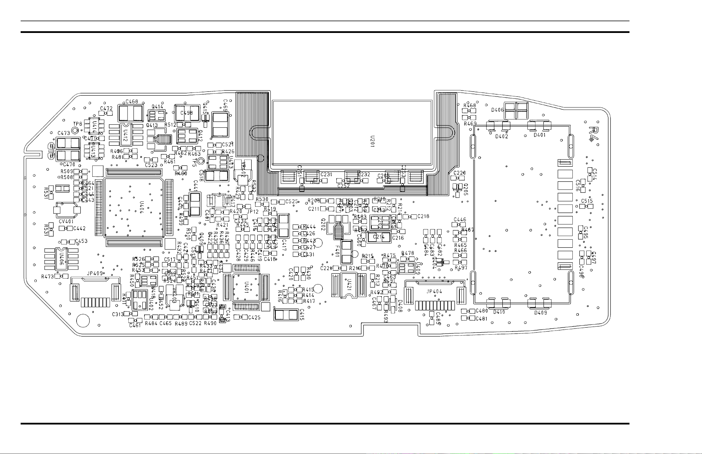
AE/LZB 119 1906 R1A
COMPONENT LAYOUT
MAIN BOARD
42
BOTTOM
Page 43

SCHEMATIC
AE/LZB 119 1906 R1A
403-440 MHz
(K501C404, R2)
43
Page 44

AE/LZB 119 1906 R1A
SCHEMATIC
440-470 MHz
(K501C401, R8)
44
Page 45

SCHEMATIC
AE/LZB 119 1906 R1A
470-512 MHz
(K501C403, R2)
45
Page 46

AE/LZB 119 1906 R1A
Ericsson Inc.
Private Radio Systems
Mountain V ie w Road
Lynchb ur g, Virginia 24502 AE/LZB 119 1906 R1A
1-800-528-7711 (Outside USA, 804-528-7711) Printed in U.S.A.
 Loading...