

Ericsson EDACS 900 Assembly

LBI-38165B
EDACS 900
MASTER OSCILLATOR ASSEMBLY
19D902127G1
TABLE OF CONTENTS
Page
SPECIFICATIONS . . . . . . . . . . . . . . . . . . . . . . . . . . . . . . . . . . . . . . . . . . . . . . . Front Cover
DESCRIPTION . . . . . . . . . . . . . . . . . . . . . . . . . . . . . . . . . . . . . . . . . . . . . . . . . . . . 1
CIRCUIT ANALYSIS . . . . . . . . . . . . . . . . . . . . . . . . . . . . . . . . . . . . . . . . . . . . . . . . 1
ADJUST MENT PROCEDURE . . . . . . . . . . . . . . . . . . . . . . . . . . . . . . . . . . . . . . . . . . . 1
PARTS LIST . . . . . . . . . . . . . . . . . . . . . . . . . . . . . . . . . . . . . . . . . . . . . . . . . . . . . 2-3
OUTLINE AND SCHEMATIC DIAGRAMS
Master Oscillator Panel . . . . . . . . . . . . . . . . . . . . . . . . . . . . . . . . . . . . . . . . . . . . . 4
OUTLINE DIAGRAM
Oscillator Board (Component Side) . . . . . . . . . . . . . . . . . . . . . . . . . . . . . . . . . . . . . . . 5
Oscillator Board (Solder Side) . . . . . . . . . . . . . . . . . . . . . . . . . . . . . . . . . . . . . . . . . . 6
SCHEMATIC DIAGRAM
Oscillator Board . . . . . . . . . . . . . . . . . . . . . . . . . . . . . . . . . . . . . . . . . . . . . . . . . 7
SERVICE SHEET
Master Oscillator Cable . . . . . . . . . . . . . . . . . . . . . . . . . . . . . . . . . . . . . . . . . . . . . 8
Test Switch Cable . . . . . . . . . . . . . . . . . . . . . . . . . . . . . . . . . . . . . . . . . . . . . . . . 8
SPECIFICATIONS*
OUTPUT LEVEL -6dBm minimum
REFERENCE FREQUENCY 17.6125 MHz +0.5 MHz
CURRENT DRAIN 1.5 Amperes maxi mum
VOLTAGE 24 Volts DC
o
TEMPERATURE RANGE -30
OUTPUT PORTS 20
*These specifications are intended primarily for use by service personnel. Refer to the appropriate Specification
Sheet for complete specifications.
C to +60oC
+20%
Printed in U . S.A.

LBI-38165
DESCRIPTION
The EDACS 900 Master Oscillator is a self -contained, high
stability reference oscillator that supplies the 17.6125 MHz
reference frequency to the transmitter and receiver frequency
synthesizers. One master oscillator provides refe rence frequencies for up to 20 trunke d repeat er statio ns at the rep eater site .
The oscillator shelf contains two identical oscillator circuits to provide high reliability. Should the primary oscillator
fail, the standby oscillator is automatically activated to provide
continuous oper ation.
Two separate power supplies are used to supply the oscillator shelf for additional reliability.
CIRCUIT ANALYSIS
Two identical high stability oscillator modules, U5 and U6,
are connect ed i n a co ld st andb y arra ngem ent. S houl d pri mar y
oscillator U6 fail, standby oscillator U5 is activated to provide
continuous operation. As the basic oscillator circuits are the
same, only the primary oscillator circuit will be described. In
addition, operation of the switching and alarm circuits, as well
as circuits common to both oscillators are included
Regulator U3, pass transistor Q9 and Zener diode VR4
provide a closely regulated 12-volt supply for oscillator module U6. The 17.6125 MHz output at U6-1 is coupled through
diode switch D5 and D6 to the input of an RF buffer/amplifier
circuit (Q3 and Q4) that provides approximately 30 dB of gain.
The output of Q4 is applied to fou r current mode drivers, U8,
U9, U10 and U11. Each of these driver stages drives five
outputs. The output jacks (J 1 t hrough J20) are mounted on t he
rear of the oscillator shelf, and provide a -6 dBm signal at
17.6125 MHz.
The output at U6-1 is also applied to a level monitor circuit
consisting of amplifier Q5, rectifier Q6 and D8,and c omparator
U7C. U7D provides the voltage reference for the level monitor
circuit. R72 adjusts the level that switches operation from
primary oscillator U6 (OSC-1) to secondary oscillator U5
(OSC-2).
When U6 is operating properly, the output at comparator
output U7C-8 is approximately 1.2 volt. This keeps switching
transistors Q5 off and Q10 on, and allows the OSC 1 indicator
LED to turn on. When Q10 is on, regulator U3 is turned off,
keeping secondary oscillator U5 turned off. If U6 should fail,
the comparator circuit switches the output at U7C-8 to approximately 10 volts. This turns on Q7 and turns off Q10, allowing
secondary oscillator U5 to start operating. The output of th e
OSC-2 comparator goes low, turning on the yellow OSC 2
indicator LED.
The OSC-2 output is coupled through the RF buffer/amplifier stage and applied to the driver stages which provide up to
20 outputs for the repeater stations.
The alarm and oscillator detector outputs are connected to
J24 to allow remote sensing of the oscillator board status. A test
switch is located in the front panel to allow manual testing of
the standby oscillator circuitry. This lead is also connected to
J22-3 to allow remote testing of the circuit.
Supply voltage for the oscillator board is provided by the 24
volt power supply. The supply voltage is applied at J23 through
steering diodes D14 and D15 from two different power supplies for reliability. The 24-volt input powers the four 12-volt
regulators on the oscillator board. Regulators U1 and U2 outputs are paralleled thro ugh diodes D1 and D2 for adde d reliability.
An alarm circuit consisting of Q11, Q12, Q13 and diodes
D18 and D19 provides a visual alarm on the front panel, and
activates a remote alarm output at J22-4. This alarm is ac tivated
if either regulator U1 or U2 fails, or if both oscillators should
fail.
If U1 or U2 fails, Q11 or Q12 will turn on. This lights the
red ALARM indicator and turns on Q14 to provide a "low"
alarm output at J22-4.
Should both oscillators stop running, the outputs at U7B7 and U7C-8 will switch to app roximately 10 volts. These
voltages will reverse bias D18 and D19, causing Q13 to turn
on. Turning on Q13 also turns on Q12, lighting the red alarm
LED. This also tur ns on Q14 applyi ng a " low" to J22- 4 fo r
the remote alarm circuit.
ADJUSTMENT PROCEDURE
Alarm adjust potentiometers R2 and R72 are the only two
adjustments on the Master Oscillator board, and will not
normally require adjustment. However, if it bec omes necessary to replace parts due to component failure or other
reasons, adjust R2 and R72 as follows:
1. Apply power to the Master Oscillator shelf and let the
oscillators warm up for about 5 minutes.
2. Turn both R2 and R72 fully counterclockwise. The
Green Osc-1 indicator (D10) and The Yellow OSC-2
indicator (D11) shou ld be OFF, and the Red ALARM
indicator (D9) should be ON.
3. Turn R2 fully clockwise. The Yellow OSC-2 indicator
should turn ON, and the Red ALARM indicator should
turn OFF.
4. Connect a 10- ohm resistor with short lea ds from pin 1 of
U5 (or C11) to ground on U5. The Yellow OSC-2
indicator should be ON, and the Red ALARM indicator
should be OFF. Then turn R2 counterclockwise until the
OSC-2 Yellow indicator turns OFF and the Red
ALARM indicator turns ON. Now remove the 10-ohm
resistor. The Yellow OSC-2 indicator should turn ON
and the Red ALARM indicator should turn OFF.
5. Next, turn R72 f ully c loc kwise . The Gre en OS C-1 indi cator should turn ON, and the Yellow and Red indicators
should turn OFF.
6 Connect the 10-ohm re sis tor (wit h shor t lea ds) from pin
1 of U6 (or C29) to ground on U6. The Green O SC-1
indicator should be ON and the Red ALARM indicator
should be OFF. Next, turn R72 counterclockwise until
the Green OSC-1 indicator turns OFF. The Yellow
OSC-2 indicator and the Red ALARM indicator should
be ON. Then remo ve the 10-ohm resistor. The Yellow
OSC-2 indicator and the Red ALARM indicator should
be OFF, and the Green OSC-1 indicator should be ON.
SYSTEM CHECKS:
1. After setting R2 and R72, measure the frequency and
output power. The fr equency should be 17.6125 M Hz
+0.5 Hz and the output power at all ports should be
greater th an -6 dBm (i nto 50 ohm s).
CAUTION
Normal test equipment is not stable enough to measure
the absolute frequency of the master oscillator. A National Bureau of Standards must be used to correctly
measure the frequency. Do not adjust the frequency
unless proper equipment is available.
2. Depress the Test Switch (or short across J21-1 and
J21-2). With the Test Switch depressed or shorted, th e
remote monitor DC voltage at J22-2 should be 9 to 10
Volts. The Green OSC-1 indicator should be OFF, the
Yellow OSC-2 indicator should be ON, and the Red
ALARM indicator should be OFF.
3. Repeat the frequency and output checks (Step 1 of
System Checks) for the standby oscillator.
Copyright© December 1988, General Electric Company
1
LBI-38165
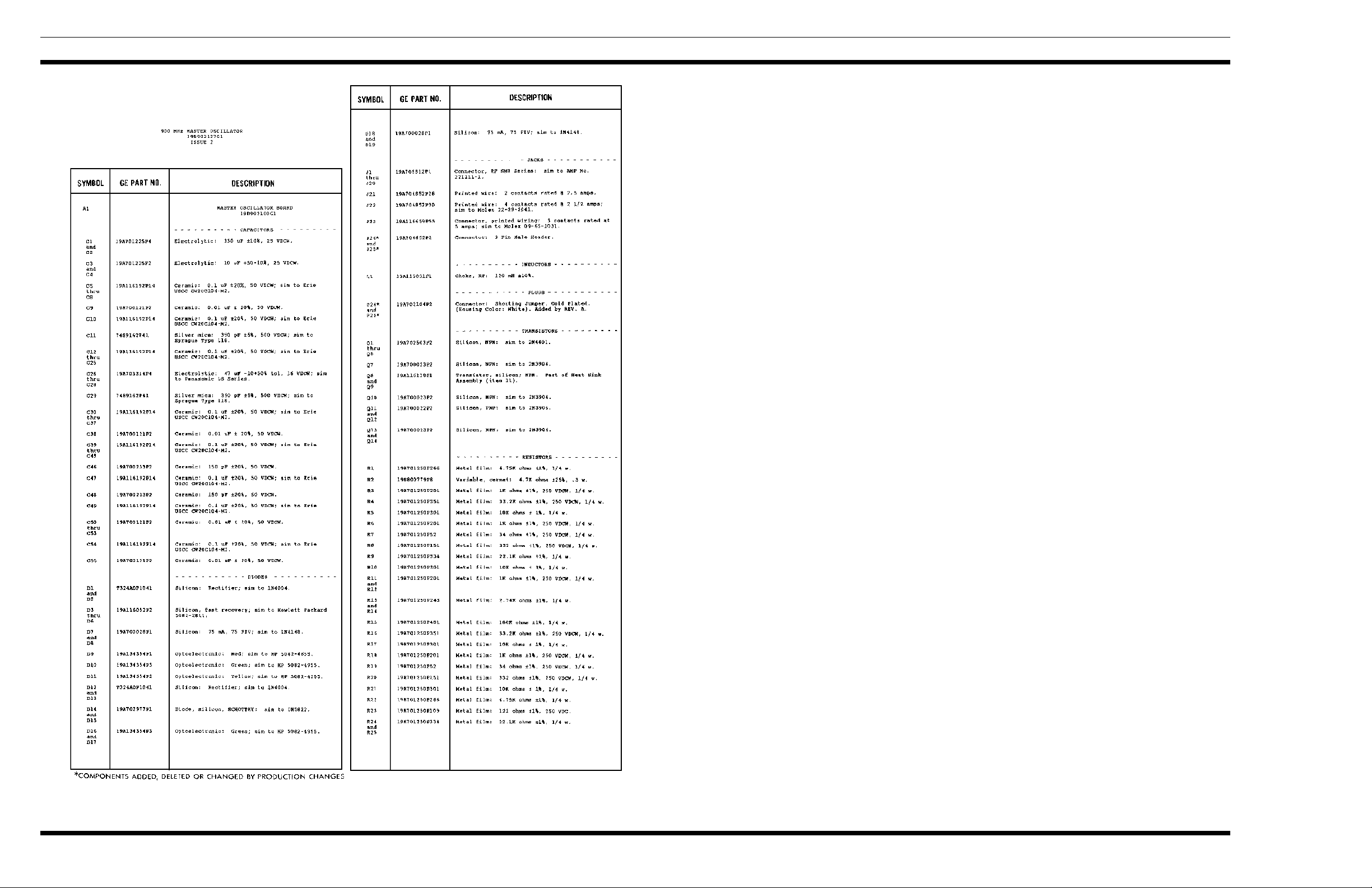
PARTS LIST
2
 Loading...