

Ericsson EDACS 19D902120G1 Maintenance Manual
Printed in U.S.A
LBI-38163B
ERICSSONZM
ERICSSONZM
Ericsson GE Mobile Communications Inc.
Mountain View Road Lynchburg Virginia 245 02
EDACS
®
900 MHz TRUNKED RECEIVER
19D902120G1
Mobile Communications
Maintenance Manual

DESCRIPTION
These receivers are doubl e conversi on, superhete rodyne,
single frequency FM receivers for operation in trunked repeater systems. The receiver utilizes monolithic crystal filters
between the IF gain stages to provide the selectivity and
intermodulation required to meet or exceed all EIA specifications for trunked receivers.
The receiver consists of the receiver board and audio
board, with audio and control functions as well as supply
voltages applied through the system board.
CIRCUIT ANAL YSIS
RECEIVER BOARD
The receiver board consists of the RF amplifier, mixer and
1st IF, 2nd IF and audio stages, and a synthesizer circuit. The
receiver board uses a co mbination of crystal and ceramic
bandpass filters for good intermodulation and desensitization
characteristics. A Block Diagram of the receiver board is
shown in Figure 1.
RF Front End
RF signal input from the antenna is applied to the receiver
board through J1. The 896-901 MHz input is c ouple d thr ough
broadband ceramic filter FL1 to RF amplifier, U1. Amplifier
U1 provides a gain of approximately 23 dB.
The amplifier output is coupled through two broadband
ceramic filters (FL2 and FL3) and applied to Mixer U2. The
mixer is a high level passive switch with a loss of approximately 6.5 dB.
First Mixer And IF
The local oscillator (LO) injection for the mixer is generated by the receiver synt hesize r lo cated on the excit er bo ard.
The 826-831 MHz LO signal from the exciter is applied to the
receiver board at J4, where it is amplified to approximately
100 milliwatts by RF Amp U3, filtered by FL4, and applied to
the 1st mixer.
The 70 MHZ mixer output is amplified by 1st IF Amplifier
U4. Two 70 MHz crystal filters, FL5 and FL6, provide the 1st
IF filtering. Adjustable coils L7 and L9 provide matching for
proper response of IF filter FL6.
Synthesizer
A synthesizer circ uit located on the re ceiver board pr ovides
the 2nd LO frequency of 70.450 MHZ. The synthesizer consists of counter U9, phase detector U10, DC amp U11, VCO
FET Q3, RF buffer amplifiers Q1, Q2 and Q4.
The high stability 17.6125 MHz reference frequency from
the master oscillator is applied to the receiver board at J2. This
reference frequency is buffered by Q1, and applied to phase
detector U10.
VCO Q3 operates at 70.450 MHz. The circuit is tuned by
L11. The output of the VCO is c oupled through b uffer amp Q4
and RF amp Q2, and applied to the div ide-by-four cou nter, U9.
The counter output is applied to phase detector U10, whose
output is applied to DC amplifier U11. Feedback for the loop
control voltage is developed across R7.
The 70.450 MHz output is coupled through C40 from the
collector of Q4 to pin 4 of audio IC , U6, , wh ere it is mixed
with the 70 MHZ 1st IF input to derive the 455 kHz 2nd IF.
Second Mixer, IF & Audio
Integrated circuit (IC) U6 contains the 2nd mixer, 2nd IF
amplifier and mixer stages, the audio detector and audio
amplifiers.
The 70 MHz 1st IF output of FL6 is applied to U6-1. The
70.450 MHz 2nd LO signal is applied to t he 2nd mixer at U6 -4
to derive the 450 kHz 2nd IF signal. The 450 kHz IF is filtered
by ceramic filters FL7 and FL8. The audio component of the
2nd IF is demodulated by the quadrature detector circuit in U6.
Network Z1 provides the required 90° phase shift of the 450
kHz signal. The de-modulated audio from U6-8 is coupled
through buffer Q5 and applied to audio output jack J3-3.
RSSI Voltage
The Received Signal Sensitivity Indication (RSSI) is a DC
level that is proportional to the receiver RF input signal level
to the receiver. This voltage can be measured at J3-4.
Copyright© December 1989, General Electric Company
TABLE OF CONTENTS
SPECIFICATIONS . . . . . . . . . . . . . . . . . . . . . . . . . . . . . . . . . . . . . . . . . . . . . . . . . . 1
DESCRIPTION . . . . . . . . . . . . . . . . . . . . . . . . . . . . . . . . . . . . . . . . . . . . . . . . . . . . 1
CIRCUIT ANALYSIS . . . . . . . . . . . . . . . . . . . . . . . . . . . . . . . . . . . . . . . . . . . . . . . . . 1
MAINTENANCE . . . . . . . . . . . . . . . . . . . . . . . . . . . . . . . . . . . . . . . . . . . . . . . . . . . 4
ADJUSTMENT PROCEDURE . . . . . . . . . . . . . . . . . . . . . . . . . . . . . . . . . . . . . . . . . . . . 5
OUTLINE DIAGRAMS
Receiver Board . . . . . . . . . . . . . . . . . . . . . . . . . . . . . . . . . . . . . . . . . . . . . . . . . 6
Audio Board 19D902181G1 . . . . . . . . . . . . . . . . . . . . . . . . . . . . . . . . . . . . . . . . . . . 8
Audio Board 19D902093G1 . . . . . . . . . . . . . . . . . . . . . . . . . . . . . . . . . . . . . . . . . . . 10
SCHEMATIC DIAGRAMS
Receiver Board . . . . . . . . . . . . . . . . . . . . . . . . . . . . . . . . . . . . . . . . . . . . . . . . . 7
Audio Board 19D902181G1 . . . . . . . . . . . . . . . . . . . . . . . . . . . . . . . . . . . . . . . . . . . 9
Audio Board 19D902093G1 . . . . . . . . . . . . . . . . . . . . . . . . . . . . . . . . . . . . . . . . . . . 11
PARTS LISTS . . . . . . . . . . . . . . . . . . . . . . . . . . . . . . . . . . . . . . . . . . . . . . . . . . . . . 12
PRODUCTION CHANGES . . . . . . . . . . . . . . . . . . . . . . . . . . . . . . . . . . . . . . . . . . . . . 13
SPECIFICATIONS*
Frequency Range 896.0125 — 900.9875 MHz
Audio Output
AUDIO PA 2 Watts at 8 Ohms
Vol/ Squelch Hi 1 Vrms @ 1.5 khz Deviation with 1 kHz modulation
Selectivity 75 dB adjacent channel
Spurious Response
Image - 80 dB minimum
All Other - 90 dB minimum
Intermodulation
Adjacent Channel - 65 dB
Alt. Channel and Beyond - 80 dB
12 dB SINAD - 120 dBm typical
Rated Output
Audio Board 19D902181G1 2 Watts
Audio Board 19D902093G1 5 Watts
Distortion Less than 5%
Frequency Stability 0.05 PPM (high stability reference)
AM Rejection - 26 dB minimum
Hum and Noise - 40 dB
*These specifications are intended primarily for use by service personnel. Refer to the appropriate Specification Sheet for
complete specifications.
The trunked 900 MHz receivers may be equip pe d
with either audio board 19D02181G1 or
19D902093G1, as the boards are di rectly interchangeable. In earlier model receivers, audio
board 19D902093G1 was used. In later model
receivers, audio board 19D902181G1 is used.
Service information for both audio boards is provided in this Maintenance Manual.
NOTE
LBI-38163
1

Supply Voltage
The receiver is supplied by a regulated 10 volts from the
system board. However, the more critical circuits are supplied by
voltage regulators U5, U7 and U8 for stability and isolation.
Regulated 10 volts from the system board is used to supply
RF amplifier U1, IF amp U4, VCO transistor Q3, and RF buffer
Q4. Regulator U5 provides the 5-volt supply for audio IC, U6,
and 5-volt regulator U7 supplies counter U9, Phase detector U10,
and RF amps Q1 and Q2. The 8-volt regulator (U8) provides
power for RF amp U3 and audio buffer Q5.
AUDIO BOARD
Audio board 19D902181G1 consists of a preamplifier cir cuit, squelch detector, audio IC and audio PA circuit. The audio
board is connected to the system board through P904. The
discriminator output is connected through J601-3 on the audio
board. Power is supplied from a regulated 10 volts from the
system board. A Block Diagram Of the audio board is shown in
Figure 2.
Audio Preamplifier
Discriminator audio from J602-3 is coupled through Audi o
Level Adjust R608 to the preamplifier circuit. The preamp consists of Q601, Q602, Q605 and associated circuitry, and provides
26 dB of gain. The amplified output is connected to the squelch
and audio hybrid ICs through the arm of the VOL and SQ
controls on the exciter-receiver door assembly.
Receiver Audio
The audio circuitry consists of a three-stage, quad integrated
circuit (U602-A, U602-C and U602-D). The th ree stages provide
a standard EIA Channel Guard tone reject filter, a receiver
de-emphasis circuit, and the low level audio driver circuitry.
Figure 1 - Receiver Board Block Diagram
Figure 2 - Block Diagram; Audio Board 19D902181G1
LBI-38163
2
Audio from the pre-amplifier circuit is coupled through the
VOLUME control to VOLUME arm (P904-13). The audio at
P904-13 is applied to CG tone reject filter U602-C, U602-D and
associated circuitry to remove any low frequency sig nal. The
filter output is then applied to a 6-dB per octave de-emphasis/audio driver circuit (U602-A). The audio driver output is
AC-coupled to the Class AB audio PA integrated circuit, U604-1.
The PA output is coupled through C633 to provide rated
power to the 8-ohm speaker. Feedback from U604-3 is coupled
through R652 and C630 to determine the gain of the audio power
amplifier. Capacitor C634 is connected across the output to
protect U604 from a "no load" or open circuit condition.
Receiver Squelch
Audio Switches
U606 is a dual section, audio switching IC that acts as two
form "C" (N.O.- N.C.) contacts. The switch states are controlled
by the inputs at U606A-10 and U606B-11. Both of the inputs are
activated by the receiver SQ DISABLE function.
When the receiver is squelched, pin 11 of U606-A is near A-.
This turns off the entire audio circuit to eliminate noise. Pin 1 of
U606-B is connected to the system board through P904-7 (RX
MUTE). This allows the receiver audio to be disabled by the
Channel Guard option when used.
Pin 2 of U606-10 is connected to the system board through
P904-6 (SQ DISABLE) so that the receiver audio stages can b e
activated for an alert tone output whenever the Carrier Controlled
Timer or other options are used.
Squelch ICs
The receiver squelch circuit consists of noise amplifier
U602B, active noise filter U601C and U601D, noise rectifier
U601B, DC amp U601A, and level detector U603D. In addition,
the squelch circuit contains the Receiver Unsquelched Sensor
(RUS) switch U603B, Carrier Activity Sensor (CAS) switch
U603A, and the RX MUTE switch U603C. The RX MUTE
switch controls the audio path to audio IC U604 through U606.
Noise Amp, Filter & Level Detector
Noise from the limiter/detector at P904-10 is coupled to the
noise amplifier U602B through the SQUELCH control, and then
applied to the active noise filter (U601C and U601D). The active
filter provides the gain and selectivity necessary to distinguish
between noise and audio. The filter output at U601D-14 drives
the level detector circuit to provide the squelch switching functions. Potentiometer R622 adjusts the noise level for the proper
squelch operation.
Squelch Switches
Level detector U603D controls two of the switched squelch
outputs. The first output controls the RX MUTE switch (U603C),
and the second output controls the CAS switch (U603A). The
RUS switch (U603B) is also controlled by the RX MUTE signal.
The squelch input to the level detector is at U603D-10.
U603D-11 is referenced to 4 Volts from voltage divider R640
and R641. When the receiver is squelched, the input at U603D10 is near 3 Volts, and the output at pin 13 is approximately 10
Volts. This keeps the output of receiver audio stages turned off,
muting the audio. The level detector output is connected to its
input through R639, providing a hysteresis loop in the squelch
circuit to prevent squelch closing on weak signals.
When the receiver is quieted by an on-frequency signal
(receiver unsquelches), the voltage at U603D-10 rises to approximately 5 Volts DC, and the ou tput at pin 14 dro ps to near 0
volts. This turns on the audio stages and sound is heard at the
speaker.
RUS Switch (Receiver Unsquelched Sensor)
When the receiver is unsquelched, the output of the level
detector (U603D-13) goes low. The low turns off U603C, causing U603B-1 to go high (approximately 10 Vdc), turning on RUS
switch U603B. The RUS output at U603B-1 is also conne cted
to the system board through P904-8 for use in special applications.
CAS Switch (Carrier Activity Sensor)
Level detector U603D also drives CAS switch U603A. When
the receiver unsquelches, the voltage at U603A-2 rises to approximately 10 volts. This voltage is connected to the system
board through P904-9 where it is used to activated such options
as the Channel Busy light, Carrier Control Timer, and Carrier
Operated Relay.
AUDIO BOARD
Audio board 19D902093G1 consists of a preamplifier cir cuit, squelch detector, audio IC and audio PA circuit. The audio
board is connected to the system board through P904. The
discriminator output is connected through J601-3 on the audio
board. Power is supplied from a regulated 10 volts from the
system board. A Block Diagram of the audio board is shown in
Figure 3.
Audio Preamplifier
Discriminator audio from J602-3 is coupled through Audi o
Level Adjust R608 to the preamplifier circuit. The preamp consists of Q601, Q602, Q605 and associated circuitry, and provides
26 dB of gain. The amplified output is connected to the squelch
and audio hybrid ICs through the arm of the VOL and SQ
controls on the exciter-receiver door assembly.
Audio IC
Hybrid audio IC U604 contains a standard EIA Channel
Guard tone reject filter, a receiver de-emphasis circuit, and the
low level audio drivers.
Audio from the VOLUME control arm is coupled through
P904-13 to pin 4 of the audio IC. The audio at U604-4 is
applied to a Channel Guard tone reject filter to remove any
low level signal. The filter output is then applied to a 6-dB per
octave de-emphasis circ uit. Th e de -empha size d out put is coupled through C635 to the differential audio driver circuit.
The driver output is DC-coupled to the base of push-pull
audio PA amplifiers Q603 and Q604. The P A output is coupled
through audio transformer T601 to provide rated power to the
8-ohm speaker. F eedback fr om windings T601 -3 and -4 dete rmine the gain of the differential audio driver in U604. Resistor
R619 and capacitor C637 in the trans former secondary protect
the PA transistors from a "no load" or open circuit conditions.
When the receiver is squelched, U604-1 drops to near A-.
This turns off the entire audio circuit to eliminate current drain.
Pin 1 of U604 is also connected to the system board through
P904-7 (RX MUTE). This disables the receiver audio whenever the Channel Guard option is used.
Pin 2 of U604 is connected to the system board through
P904-6 (SQ DISABLE) so that the receiver audio stages can
be activated for an alert tone output whenever the Carrier
Controlled Timer or oth er options are used.
Figure 3 - Block Diagram; Audio Board 19D902093G1
LBI-38163
3
Squelch IC
Squelch hybrid U603 contains the noise amplifier, active
noise filter, detector, slow and fast squelch circuits, the Receiver Unsquelched Sensor (RUS), and the Carrier Activity
Sensor (CAS) switch.
Noise from the quadrature detector is coupled through the
audio preamp to the SQUELCH control,and then through
P904-10 to pins 1 and 2 on Squelch IC U603. The input is then
applied to the noise amplifier and active filter to provide the
gain and selectivity necessary to distinguish between noise and
audio. The filter output is applied to external noise amplifier
U601 which provides the extra noise gain required for narrow
band signals. The amplifier output at U601-1 drives the active
detector circuits in U603 to provide the squelch switching
functions.
Thermistor RT601 keeps the input to the active detector
constant over wide variations in te m perature. R622 is used to
set the noise level for proper squelch operation.
With a signal below the 20 dB quieting level, the slow
squelch circuit provides a conventional (200 millisecond)
slow squelch operation to prevent rapid squelch opening and
closing in weak signal areas. Service Note: In station applications,the fast squelch function is disabled by removing C360.
RX Mute
The squelch RX MUTE output at U603-7 is connected to
pin 1 of audio IC, U604. When the receiver is squelche d, the
output at U603-7 is near A-. This keeps the differential audio
driver turned off, muting the receiver.
When the receiver is quieted by an on-frequency signal
(receiver unsquelches), the voltage at U603-7 rises to approximately 10 volts. This turns on the audio driver and audio PA
so that sound is heard at the speaker.
RUS Switch (Receiver Unsquelched Sensor)
With the receiver unsquelched, the output of the squelch
switch in U603 turns on the RUS switch. Th RUS switch
output is connected to the noise amplifier stage, providing the
hysteresis loop in the squelch circuit. The RUS output (when
unsquelched) increases the gain of the noise amp, ppreventing
squelch closing on weak signals. The RUS output at U603-8
is also connected to the system board through P904 -8 for use
in special applications.
CAS Switch (Carrier Activity Sensor)
The squelch in U603 also drives the CAS switch in the IC.
When the receiver unsquelches, the voltage at U603-6 rises to
approximately 10 volts This voltage is connected to the system
board through P904-9 where it is used to activated such
options as the Channel Busy light, Carrier Control Timer, a nd
Carrier Operated Relay.
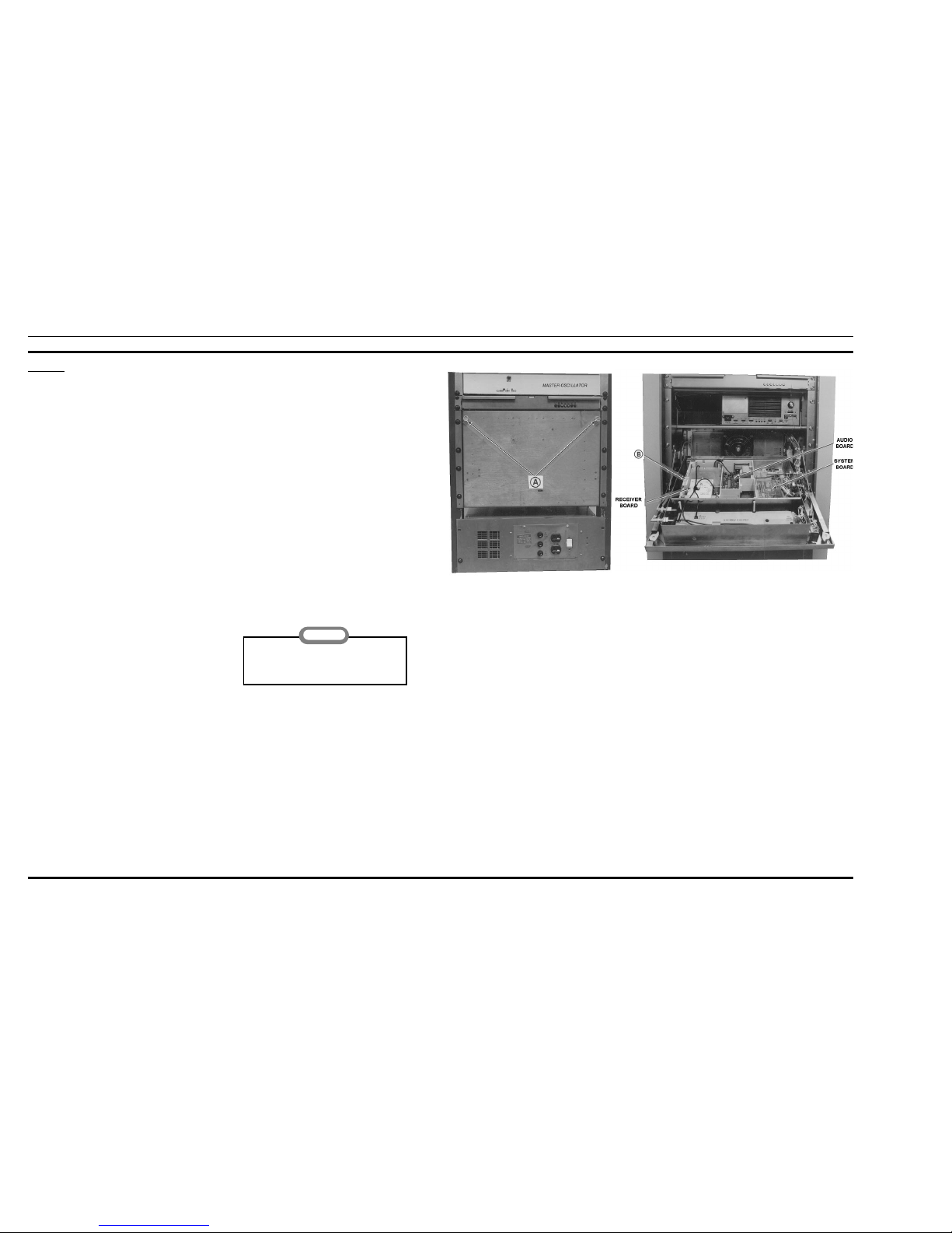
MAINTENANCE
SERVICING
To gain access to the receiver for servicing, refer to the
following procedure (see Figure 4).
To service the receiver from the top:
1. Turn the two latching knobs "A" counterclockwise to
unlatch the radio housing door as shown in Figure 4.
2. Swing the radio housing down as shown in Figure 5
and remove the top cover.
To service the receiver from the bottom:
1. Turn the two latching knobs "A" counterclockwise to
unlatch the radio housing and swing the housing down
as shown.
2. Remove the top cover. Then grasp the receiver handle
"B" and swing the housing up for access to the bottom
of the receiver.
There are only four controls that require adjustment during
system adjustment. Refer to the system adjustment procedure
contained in GETC Maintenance Manual, LBI-38164.
TROUBLESHOOTING
Both the Schematic and Outline diagrams contain troubleshooting information to assist in servicing the receiver. This
service information includes voltage and gain readings, power
levels and signal flow information. Refer to these diagrams
when troubleshooting the receiver (see Table of Contents).
ADJUSTMENTS
The receiver has no adjustments for "peaking" up receiv er
performance. If some adjustment is required as a result of
component replacement or other maintenance, refer to the
Adjustment Procedure listed in the Table of Contents.
Remove the two RF cables connecting the receiver and exciter before raising the receiver housing as directed in Step 2.
CAUTION
Figure 3 - Access To Knobs Securing Door
Figure 4 - Access To Receiver (Top and Bottom)
LBI-38163
4
 Loading...