

Page 1
L’esprit Modem
User Guide
GenLoc 354e
Reference
Revision
Date
: EG_GenLoc354e_1040Q_UG_002_UK
: 002
: 13/07/2016
http://www.ercogener.com
Dct_427_02
Page 2

EG_GenLoc354e_1040Q_UG_002_UK Page 2 / 69
Document History
Rev. Modifications Author Date Validation Date
000 Creation YST 01/07/2015 PBR 06/07/2015
001 Minor adjustment on DoC EFO 02/11/2015 PBR 03/11/2015
002 Update DoC YST 13/07/2016 MSU 13/07/2016
The main modifications of this document compared to the previous version are easily identifiable on the
screen by the blue color of the text.
Descriptions and non-contractual illustrations in this document are given as an indication only.
ERCOGENER reserves the right to make any modifications.
Dct_427_02
Page 3

EG_GenLoc354e_1040Q_UG_002_UK Page 3 / 69
TABLE OF CONTENTS
PRESENTATION ............................................................................................................................................. 10
WARNING ....................................................................................................................................................... 11
COPYRIGHT ................................................................................................................................................... 12
SYMBOLS USED ............................................................................................................................................ 13
1 SECURITY RECOMMENDATIONS ....................................................................................................... 14
1.1 GENERAL SECURITY ......................................................................................................................... 14
1.2 SECURITY IN A VEHICLE .................................................................................................................... 15
1.3 CARE AND MAINTENANCE .................................................................................................................. 15
1.4 YOUR RESPONSIBILITY ...................................................................................................................... 15
2 PRESENTATION .................................................................................................................................... 16
2.1 CONTENT .............................................................................................................................. ........... 16
2.2 MODEM PACKAGING ......................................................................................................................... 16
2.3 MECHANICAL CHARACTERISTICS ....................................................................................................... 17
2.3.1 Fixing brackets ......................................................................................................................... 17
2.4 CHARACTERISTICS AND SERVICES .................................................................................................... 18
2.4.1 Services .................................................................................................................................... 18
2.5 ENVIRONMENTAL CHARACTERISTICS ................................................................................................. 21
3 INTERFACES ......................................................................................................................................... 22
3.1 FRONT SIDE ...................................................................................................................................... 22
3.2 BACK SIDE ....................................................................................................................................... 23
3.3 FUNCTIONAL ARCHITECTURE ............................................................................................................. 24
3.4 POWER SUPPLY ................................................................................................................................ 25
3.4.1 Power supply cables ............................................................................................................... 25
3.4.2 Power supply 8 – 32VDC ........................................................................................................... 25
3.4.2.1 Internal battery ................................................................................................................ 26
3.4.2.2 Consumption of the GenLoc 354e ................................................................................. 27
3.4.2.3 Power Dimensioning ....................................................................................................... 28
3.5 ONE WIRE BUS .............................................................................................................................. .. 29
3.5.1 One Wire Bus ........................................................................................................................... 29
3.5.2 Option Multi 1- Wire Bus S0470C ........................................................................................... 30
3.6 ANALOG INPUTS ANA1 AND ANA2 ................................................................................................... 31
3.6.1 Analog inputs 0 – 10 VDC ......................................................................................................... 31
3.6.2 Option analog inputs 4 – 20 mA S0475C ............................................................................... 32
3.7 OPTO-COUPLED INPUTS .................................................................................................................... 33
3.8 ISOLATED OPTO-COUPLED INPUTS ..................................................................................................... 34
3.9 DIGITAL OUTPUTS ............................................................................................................................. 35
Descriptions and non-contractual illustrations in this document are given as an indication only.
ERCOGENER reserves the right to make any modifications.
Dct_427_02
Page 4

3.10 POWER SUPPLY OUTPUT V
EG_GenLoc354e_1040Q_UG_002_UK Page 4 / 69
........................................................................................................... 36
BAT
3.11 BUZZER ........................................................................................................................................... 37
3.12 INPUT COMPATIBLE K-LINE (ISO 9141-2) ......................................................................................... 38
3.13 SERIAL LINK RS232_0 ..................................................................................................................... 39
3.14 SERIAL LINK RS232_1 ..................................................................................................................... 40
3.15 SERIAL LINK RS232_2 / BUS CAN OPTION ....................................................................................... 41
3.15.1 Serial link RS232_2 option S0469B ................................................................................... 41
3.15.2 Bus CAN MCP2515 option S0467D .................................................................................... 42
3.16 POWER SUPPLY POWER_OUT ........................................................................................................... 43
3.17 BOOT ............................................................................................................................................. 44
3.18 RESET ........................................................................................................................................... 45
3.19 ACCELEROMETER ............................................................................................................................. 46
3.20 SIM CARD ........................................................................................................................................ 46
3.21 DUAL SIM OPTION – S0471C ........................................................................................................... 46
3.22 LEDS OF THE MODEM ........................................................................................................................ 47
3.22.1 GSM Led ............................................................................................................................... 47
3.22.1.1 Without application ......................................................................................................... 47
3.22.1.2 With standard library EGM ............................................................................................. 47
3.22.1.3 The application ERCOGENER EaseLoc_Vx ................................................................. 47
3.22.1.4 Owner application ........................................................................................................... 47
3.22.2 User Led ............................................................................................................................... 48
3.22.3 GNSS Led ............................................................................................................................. 48
4 GSM EXTERNAL ANTENNA ................................................................................................................. 49
5 GNSS EXTERNAL ANTENNA ............................................................................................................... 50
5.1 INSTALLATION OF GNSS EXTERNAL ANTENNA ................................................................................... 51
6 USE OF THE MODEM ............................................................................................................................ 52
6.1 SPECIFIC RECOMMENDATIONS FOR THE USE OF THE MODEM IN VEHICLES ............................................ 52
6.1.1 Recommended connection on the battery of a truck ........................................................... 52
6.2 TURNING THE MODEM OFF ............................................................................................................... 53
6.3 STARTING WITH THE MODEM .............................................................................................................. 54
6.3.1 Mounting the modem ............................................................................................................... 54
6.3.2 SIM card installation ................................................................................................................ 54
6.4 USE OF THE MODEM .......................................................................................................................... 55
6.4.1 Checking the communication with the modem .................................................................... 55
6.4.1.1 Without application ......................................................................................................... 55
6.4.1.2 Standard Library .............................................................................................................. 56
6.4.1.3 The application ERCOGENER EaseLoc_Vx ................................................................. 56
6.4.1.4 The owner application .................................................................................................... 57
6.5 CHECKING THE QUALITY OF THE GSM RECEPTION SIGNAL.................................................................. 57
6.6 VERIFICATION OF THE PIN CODE ....................................................................................................... 58
6.7 VERIFICATION OF THE MODEM REGISTRATION ON GSM NETWORK ....................................................... 58
Descriptions and non-contractual illustrations in this document are given as an indication only.
ERCOGENER reserves the right to make any modifications.
Dct_427_02
Page 5

EG_GenLoc354e_1040Q_UG_002_UK Page 5 / 69
6.8 VERIFICATION OF THE MODEM REGISTRATION ON GPRS NETWORK ..................................................... 59
6.9 READING A CURRENT POSITION GIVEN BY THE GNSS ......................................................................... 60
7 RECOMMENDED ACCESSORIES ........................................................................................................ 62
8 CLIENT SUPPORT ................................................................................................................................. 62
ANNEX 1 – 4-PINS MICRO-FIT CABLE (4 WIRES, POWER SUPPLY) ....................................................... 63
ANNEX 2 - 14-PINS MICRO-FIT CABLE (INPUTS/OUTPUTS) .................................................................... 64
ANNEX 3 – 16-PINS MICRO-FIT CABLE (14 WIRES, SERIAL LINKS) ....................................................... 65
ANNEX 4 – 16-PINS MICRO-FIT CABLE (16 WIRES, SERIAL LINKS, BOOT AND RESET) .................... 66
ANNEX 5 - ABBREVIATIONS ........................................................................................................................ 67
DECLARATION OF CONFORMITY ............................................................................................................... 69
Descriptions and non-contractual illustrations in this document are given as an indication only.
ERCOGENER reserves the right to make any modifications.
Dct_427_02
Page 6

EG_GenLoc354e_1040Q_UG_002_UK Page 6 / 69
Index of Tables
Table 1 : Mechanical characteristics ............................................................................................................... 17
Table 2 : Characteristics and services ............................................................................................................. 18
Table 3: Environmental characteristics ............................................................................................................ 21
Table 4 : Front side connection ....................................................................................................................... 22
Table 5 : Effects of power supply defect .......................................................................................................... 25
Table 6 : Characteristics of the polymer lithium battery .................................................................................. 26
Table 7 : Power supply range .......................................................................................................................... 27
Table 8: Consumption in Low Power mode @ 25 °C without battery charging .............................................. 27
Table 9 : Consumption in attached mode @ 25 °C without battery charging ................................................. 27
Table 10 : Consumption in data transfer @ 25 °C without battery charging ................................................... 27
Table 11 : Consumption in data transfer @ 25 °C without battery charging ................................................... 28
Table 12: Consumption of the battery charge @ 25 °C .................................................................................. 28
Table 13: One Wire Bus description ................................................................................................................ 29
Table 14 : One Wire Bus – Electrical characteristics ...................................................................................... 29
Table 15 : Multi 1- Wire Bus description S0470C ............................................................................................ 30
Table 16 : Multi 1- Wire Bus – Electrical characteristics S0470C ................................................................... 30
Table 17 : Description of analog inputs 0 – 10 V ............................................................................................. 31
Table 18 : Characteristics of analog inputs 0 – 10 V ....................................................................................... 31
Table 19 : Description of analog inputs 4 – 20 mA .......................................................................................... 32
Table 20 : Characteristics of analog inputs 4 – 20 mA .................................................................................... 32
Table 21 : Description of opto-coupled inputs ................................................................................................. 33
Table 22 : Characteristics of opto-coupled inputs ........................................................................................... 33
Table 23 : Description of isolated opto-coupled inputs .................................................................................... 34
Table 24 : Characteristics of isolated opto-coupled inputs .............................................................................. 34
Table 25 : Description of digital outputs .......................................................................................................... 35
Table 26 : Characteristics of open collector output ......................................................................................... 35
Table 27 : Description of the power supply V
Table 28 : Conditions of use of the power supply output V
............................................................................................. 36
BAT
........................................................................ 36
BAT
Table 29 : Description of buzzer output ........................................................................................................... 37
Table 30 : Characteristics of buzzer output ..................................................................................................... 37
Table 31 : Example of Transducer tested with the GenLoc 354e ................................................................... 37
Table 32 : Description of the input compatible K-Line (ISO 9141-2) ............................................................... 38
Table 33 : Bus K-Line for a tachograph ........................................................................................................... 38
Table 34 : Pins description of serial link RS232_0 .......................................................................................... 39
Table 35 : Characteristics of serial link RS232_0 ............................................................................................ 39
Table 36 : Pins description of serial link RS232_1 .......................................................................................... 40
Table 37 : Characteristics of serial link RS232_1 ............................................................................................ 40
Table 38 : Pins description of serial link RS232_2 .......................................................................................... 41
Table 39 : Characteristics of serial link RS232_2 ............................................................................................ 41
Table 40 : Pins description of the link Bus CAN option S0467D ..................................................................... 42
Descriptions and non-contractual illustrations in this document are given as an indication only.
ERCOGENER reserves the right to make any modifications.
Dct_427_02
Page 7

EG_GenLoc354e_1040Q_UG_002_UK Page 7 / 69
Table 41 : Characteristics of serial link Bus CAN MCP2515 option S0467D .................................................. 42
Table 42 : Description of Power_Out ............................................................................................................... 43
Table 43 : Characteristics of Power_Out ......................................................................................................... 43
Table 44 : Description of BOOT input .............................................................................................................. 44
Table 45 : Conditions of use of BOOT signal .................................................................................................. 44
Table 46 : Description of RESET input ............................................................................................................ 45
Table 47 : Conditions of use of RESET signal ................................................................................................ 45
Table 48: Characteristic of accelerometer ....................................................................................................... 46
Table 49: Characteristics of the SIM card power voltage ................................................................................ 46
Table 50: Characteristics of the 2nd SIM card power voltage .......................................................................... 46
Table 51: Status of GSM LED ......................................................................................................................... 47
Table 52: Available status of GNSS LED ........................................................................................................ 48
Table 53 : Characteristics of GSM external antenna ....................................................................................... 49
Table 54 : Characteristics of GNSS external antenna ..................................................................................... 50
Table 55 : RSSI value ...................................................................................................................................... 57
Table 56 : Verification of PIN code .................................................................................................................. 58
Table 57 : Verification of modem registration on GSM network ...................................................................... 58
Table 58 : Verification of the modem registration on GPRS network .............................................................. 59
Table 59 : Reading a current position given by the GNSS .............................................................................. 61
Table 60 : Characteristics of power supply cable ............................................................................................ 63
Table 61 : Characteristics of 14-wire inputs/outputs cable .............................................................................. 64
Table 62 : Wiring of the 14-wire inputs/outputs cable ..................................................................................... 64
Table 63 : Characteristics of 14-wires serial links cable .................................................................................. 65
Table 64 : Wiring of 14-wires serial links cable ............................................................................................... 65
Table 65 : Characteristics of the 16-wires serial links cable (Boot + Reset) ................................................... 66
Table 66 : Wiring of the 16-wires serial links cable (Boot + Reset) ................................................................. 66
Descriptions and non-contractual illustrations in this document are given as an indication only.
ERCOGENER reserves the right to make any modifications.
Dct_427_02
Page 8

EG_GenLoc354e_1040Q_UG_002_UK Page 8 / 69
Index of Figures
Figure 1 : Content ............................................................................................................................................ 16
Figure 2 : Dimensions ...................................................................................................................................... 17
Figure 3 : Back side ......................................................................................................................................... 17
Figure 4 : Front side ......................................................................................................................................... 22
Figure 5 : Back side ......................................................................................................................................... 23
Figure 6 : Functional architecture .................................................................................................................... 24
Figure 7 : Consumption max ........................................................................................................................... 28
Figure 8 : Internal electrical scheme of the One Wire bus .............................................................................. 29
Figure 9 : Internal electrical scheme of the Multi 1- Wire Bus S0470C ........................................................... 30
Figure 10 : Internal electrical scheme of analog input 0 – 10 V ...................................................................... 31
Figure 11 : Internal electrical scheme of analog input 4 – 20 mA ................................................................... 32
Figure 12 : Internal electrical scheme of opto-coupled inputs ......................................................................... 33
Figure 13 : Internal electrical scheme of isolated inputs ................................................................................. 34
Figure 14 : Internal electrical scheme of the output ........................................................................................ 35
Figure 15 : Example of relay control ................................................................................................................ 35
Figure 16 : Example of Transducer tested with the GenLoc 354e .................................................................. 37
Figure 17 : Internal electrical scheme of the K-Line bus for a tachograph ...................................................... 38
Figure 18 : Level of K-Line bus for a tachograph ............................................................................................ 38
Figure 19 : Scheme for connection of K-Line input to tachograph .................................................................. 38
Figure 20 : Standards signals of serial link RS232_0 ...................................................................................... 39
Figure 21 : Standards signals of serial link RS232_1 ...................................................................................... 40
Figure 22 : Standards signals of serial link RS232_2 ...................................................................................... 41
Figure 23 : Output signal of bus CAN MCP2515 option S0467D .................................................................... 42
Figure 24 : Standards signals of link Bus CAN MCP2515 option S0467D ..................................................... 42
Figure 25 : Internal electrical scheme of Power_Out ...................................................................................... 43
Figure 26 : Drop of voltage .............................................................................................................................. 43
Figure 27 : Internal electrical scheme of BOOT .............................................................................................. 44
Figure 28 : Internal electrical scheme of RESET ............................................................................................ 45
Figure 29 : Chronogram of RESET signal ....................................................................................................... 45
Figure 30 : Positioning of the accelerometer axis ........................................................................................... 46
Figure 31 : Back side Leds .............................................................................................................................. 47
Figure 32 : GSM external antenna .................................................................................................................. 49
Figure 33 : GNSS external antenna ................................................................................................................ 50
Figure 34 : Recommended installation of GNSS antenna ............................................................................... 51
Figure 35 : Installation of GNSS antenna not recommended .......................................................................... 51
Figure 36 : Recommended connection on the battery of a truck .................................................................... 52
Figure 37 : Mounting the modem ..................................................................................................................... 54
Figure 38 : Installation of the modem .............................................................................................................. 54
Figure 39 : 4-pins Micro-FIT cable ................................................................................................................... 63
Figure 40 : Fuse Mini Blade ............................................................................................................................. 63
Descriptions and non-contractual illustrations in this document are given as an indication only.
ERCOGENER reserves the right to make any modifications.
Dct_427_02
Page 9

EG_GenLoc354e_1040Q_UG_002_UK Page 9 / 69
Figure 41 : 14-pin Micro-FIT cable (Inputs/Outputs) ....................................................................................... 64
Figure 42 : 16-pins Micro-FIT cable (Serial links) ............................................................................................ 65
Figure 43 : 16-wire Micro-FIT cable (Serial links, Boot and Reset) ................................................................. 66
Descriptions and non-contractual illustrations in this document are given as an indication only.
ERCOGENER reserves the right to make any modifications.
Dct_427_02
Page 10

EG_GenLoc354e_1040Q_UG_002_UK Page 10 / 69
Presentation
Entirely dedicated to geolocation and embedded data services, the modem GenLoc 354e combines the
GSM / GPRS / HSPA and GNSS functions in the same robust casing.
The GNSS data can be transmitted by SMS or data communication GSM/GPRS/HSPA.
This product includes the 72-channel GNSS function. The high sensitivity GNSS solution ensures the data
collection in difficult environments.
The modem is Quad-Bands (850/900/1800/1900 MHz) GSM/GPRS Class 12.
The modem is six-bands (I, II, IV, V, VI, VIII) UMTS / HSPA.
The GenLoc 354e provides 3 operating modes depending on the embedded application:
External mode (standard): The control is done by an external application. The modem is used with
the AT command set (see Commands List EG_EGM_CL_xxx_yy of ERCOGENER).
Autonomous mode: Once configured, the modem is autonomous; it cyclically registers the positions
and automatically transmits them to the client’s application via different services: SMS, GSM Data,
TCP socket GPRS/UMTS (see EG_EaseLoc_Vx_CL_yyy_UK of ERCOGENER).
Specific development mode: the EGM development tool allows the development of additional and
customized embedded applications. For more information about the tools and the training, please
contact our sales department.
Its protocols of IP connectivity integrated in the embedded application EaseLoc_Vx, are also available under
EGM libraries for a specific development, allowing a quick installation of embedded telematics solutions with
strong added-value.
This document describes the modem and provides the following information:
- General presentation,
- Functional description,
- Available basic services,
- Installation and use of the modem (first level),
- Recommended accessories for the use of the modem.
For more information about this document, ERCOGENER puts at your disposal the following elements:
- Commands List
External Mode EG_EGM_CL_xxx_yy
Autonomous Mode EG_EaseLoc_Vx_CL_yyy_UK
- Application Note EG_GenLoc354e_1040_AN_xxx_yy
- Release Note EG_GenLoc354e_1040_RL_xxx_yy
- Client Support (Hot-Line)
Descriptions and non-contractual illustrations in this document are given as an indication only.
ERCOGENER reserves the right to make any modifications.
Dct_427_02
Page 11

EG_GenLoc354e_1040Q_UG_002_UK Page 11 / 69
Warning
• ERCOGENER recommends to read carefully all documents linked to the product GenLoc 354e (User
Guide, Application Notes, Command List) that can be download on our website www.ercogener.com
.
• ERCOGENER cannot be held responsible for:
- The problems due to an inappropriate use of the GenLoc 354e.
- The problems due to a wrong configuration
- The problems due to a wrong use of an embedded software application developed or supplied by a
third party.
- The dysfunctions due to the absence or a bad coverage of the GSM, GPRS and GNSS networks.
- The dysfunctions if the product is used for the watching of physical persons where human life is
engaged.
• ERCOGENER reserves the right to modify the functions of its products "GenLoc 354e" and "EaseLoc"
without previous notice.
- To avoid any risk of electrocution, do not open the casing.
- For any functioning, the casing must be closed.
- No internal part can be repaired by the user. The GenLoc 354e must be returned to the factory for any
repair.
- The GenLoc 354e must be placed in a normally ventilated area, out of sources of heat.
- In order to guarantee the electromagnetic compatibility, the length of the serial cable, the power supply
cable and the inputs/outputs cable must not exceed 3 meters.
- The GenLoc 354e must not be connected directly to the mains supply; a voltage adapter must be used.
SCRAP THE WORN BATTERIES ACCORDING TO INSTRUCTIONS.
Descriptions and non-contractual illustrations in this document are given as an indication only.
ERCOGENER reserves the right to make any modifications.
Dct_427_02
Page 12

EG_GenLoc354e_1040Q_UG_002_UK Page 12 / 69
Copyright
The reproduction, transfer, distribution or storage of part or the totality of the contents of this document, in
any form, without the prior written authorization of ERCOGENER is strictly prohibited.
GenLoc 354e is a trademark of ERCOGENER.
Hayes is a registered trademark of Hayes Microcomputer Product Inc. The names of products and
companies mentioned in this document may be names or trademarks of their respective holders.
The use of some products or services described in this document may require a paying subscription. The
availability of some products or services described in this document may change, depending on the
configurations and the materials.
In some countries, restrictions of use of the devices may be applied. For more information, thank you to
contact your nearest legally qualified local government representative.
ERCOGENER follows a method of continuous development. Consequently, ERCOGENER reserves the right
to change and improve any of its products described in this document, without notice.
The contents of this document are provided “as it is”. Except for the applicable obligatory laws, no guarantee
in any form, explicit or implicit, including but without being limited to it the implicit guarantees of aptitude to
marketing and of appropriateness to a particular use, is granted concerning the precision, the liability or the
contents of this document. ERCOGENER reserves the right to revise or withdraw this document at any time
and without notice.
ERCOGENER cannot be held responsible for any loss of data or income, as well as particular
damage, incidental, consecutive or indirect.
Descriptions and non-contractual illustrations in this document are given as an indication only.
ERCOGENER reserves the right to make any modifications.
Dct_427_02
Page 13

EG_GenLoc354e_1040Q_UG_002_UK Page 13 / 69
Symbols used
The following symbols are used to highlight the important information of this document.
A symbol for the essential information linked to the module integration and performance.
A warning symbol indicates the actions that could harm or damage the module
Descriptions and non-contractual illustrations in this document are given as an indication only.
ERCOGENER reserves the right to make any modifications.
Dct_427_02
Page 14

EG_GenLoc354e_1040Q_UG_002_UK Page 14 / 69
1 Security recommendations
1.1 General security
It is important to respect the specific regulations linked with the use of radio equipment, in particular with the
possible risks of interference due to radio frequency (RF). Please respect carefully the following security
recommendations.
Turn OFF your GSM modem:
On an aircraft, the use of cellular telephones can endanger the plane operations; disturbing the
cellular network is illegal. The non-observance of this instruction can lead to the suspension or the
exclusion of the cellular phone services, or even to a trial, or both,
At a refueling station,
In any area with a potential explosive atmosphere that could cause an explosion or a fire,
In hospitals and other places where medical equipment may be used.
Restrictions of use of radio equipment in:
Fuel warehouses,
Chemical factories,
Places where destruction operations are in the running,
Other places where signs indicate that the use of cellular phones is prohibited or dangerous.
Other places where you should normally turn OFF the engine of your vehicle.
There can be a danger associated with the use of your GSM modem close to insufficiently protected medical
equipment such as audio devices and pacemakers.
Consult the manufacturers of medical equipment to know if it is adequately protected.
Using your GSM modem close to other electronic equipment may also cause interferences if the equipment
is insufficiently protected.
Pay attention to the warnings and the recommendations of the manufacturers.
The modem is designed to be used with "fixed" and "mobile" applications:
“Fixed" application: The GSM modem is physically linked to a site and it is not possible to move it
easily to another site.
"Mobile" application: The GSM modem is designed to be used in various places (other than fixed) and
is intended to be used in portable applications.
The modem must be used at more than 20cm from the human body.
This equipment is supplied in Very Low Security Voltage and at non-dangerous energy level.
Descriptions and non-contractual illustrations in this document are given as an indication only.
ERCOGENER reserves the right to make any modifications.
Dct_427_02
Page 15

EG_GenLoc354e_1040Q_UG_002_UK Page 15 / 69
1.2 Security in a vehicle
Do not use your Modem whilst driving, unless equipped with a correctly installed ear-piece/hands-free kit.
Respect the national regulations linked with the use of cellular telephones in vehicles. Road safety is always
a priority.
An incorrect installation of the GSM modem in a vehicle could cause an incorrect functioning of the vehicle’s
electronics. To avoid such problems, make sure that the installation was made by a qualified person. During
the installation, a verification of the electronic protection system of the vehicle must be done.
The use of a warning equipment that activates the headlights or the horn of a vehicle on a public highway is
not authorized.
1.3 Care and maintenance
The following suggestions will help you to preserve this product for many years.
Do not expose the modem to the extreme environments, to high temperature or high humidity.
Do not use or store the modem in dusty or dirty places, it could be damaged.
Do not try to disassemble the modem, at the risk of cancelation of the guarantee.
Do not expose the modem to water, rain or spilled beverage, it is not impermeable.
Avoid dropping, striking, or shaking the modem violently. The lack of care can damage it.
Do not place the modem next to computer disks, credit or travel cards or other magnetic supports. The
information contained on disks or cards can be affected by the modem.
The use of other equipment or accessories not made or not authorized by ERCOGENER can cancel the
warranty of the modem.
The battery is not covered by the warranty.
1.4 Your responsibility
This modem is under your responsibility. Treat it with care, it is not a toy. Keep it always in a secure place
and out of the reach of children.
Try to remember your PIN and PUK codes. Familiarize yourself with the modem and use the security
functions to lock it in case of non-authorized use or in case of theft.
Descriptions and non-contractual illustrations in this document are given as an indication only.
ERCOGENER reserves the right to make any modifications.
Dct_427_02
Page 16
2 Presentation
2.1 Content
The GenLoc 354e is supplied with:
- a GenLoc 354e cardboard packaging,
- a modem GenLoc 354e,
- 2 fixing brackets,
- a 4-wire power supply cable, input/output (Red/Black/Yellow/Brown) stripped with fuse.
- a stripped cable with a 14-pin connector equipped, (Inputs/Outputs).
- a stripped cable with a 16-pin connector equipped (14 wires, Serial link).
- a technical sheet (Instructions Sheet).
EG_GenLoc354e_1040Q_UG_002_UK Page 16 / 69
Figure 1 : Content
2.2 Modem packaging
The external dimensions of the modem packaging are:
- Width ................. : 160 mm,
- Height ................ : 280 mm,
- Length ............... : 64 mm.
- Weight ............... : 785 g
Descriptions and non-contractual illustrations in this document are given as an indication only.
ERCOGENER reserves the right to make any modifications.
Dct_427_02
Page 17
EG_GenLoc354e_1040Q_UG_002_UK Page 17 / 69
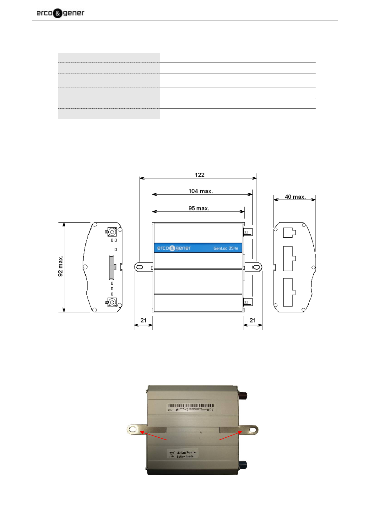
2.3 Mechanical characteristics
Table 1 : Mechanical characteristics
Dimensions
Complete dimensions
Weight
Volume
Casing
Waterproof level
95 x 92 x 40 mm (connectors excluded)
104 x 92 x 40 mm
206 grams (modem only)
< 618 grams (modem + brackets + cables)
382 cm³
Aluminium profile
IP31
The illustration below shows the dimensions of the modem including the clearances necessary for the
installation of the modem.
Figure 2 : Dimensions
2.3.1 Fixing brackets
2 brackets to fix the modem on a support.
Descriptions and non-contractual illustrations in this document are given as an indication only.
ERCOGENER reserves the right to make any modifications.
Figure 3 : Back side
Fixing brackets
Dct_427_02
Page 18

EG_GenLoc354e_1040Q_UG_002_UK Page 18 / 69
2.4 Characteristics and Services
2.4.1 Services
The GenLoc 354e is made:
• A GSM/GPRS/EDGE/UMTS modem class12 dedicated to the transmission of binary data in
asynchronous and SMS.
• A GNSS module dedicated to position tracking.
The modem characteristics and the available services are summarized in the table below.
Table 2 : Characteristics and services
Functions 3G UMTS / HSPA - 2G GSM / GPRS / EDGE
• WCDMA / HSPA 800/850/900/1700/1900/2100 MHz (Bands VI, V, VIII, IV, II, I)
3GPP Release 7
5.76 Mb/s uplink, 7.2 Mb/s downlink
• GSM 4 band 850 / 900 / 1800 / 1900 MHz (support GSM / E-GSM / DCS / PCS)
3GPP Release 7
PBCCH support
• GPRS Class 12, CS1-CS4 - up to 86.5 kb/s
• EDGE Class 12, MCS1-9 - up to 236.8 kb/s
• CSD GSM max 9.6 kb/s
UMTS max 64 kb/s
• SMS MT/MO PDU / Text mode
• WCDMA / HSDPA Power Class 3 (24 dBm)
• GSM / GPRS Power Class 4 (33 dBm) for GSM/E-GSM bands
Power Class 1 (30 dBm) for DCS/PCS bands
• EDGE Power Class E2 (27 dBm) for GSM/E-GSM bands
Power Class E2 (26 dBm) for DCS/PCS bands
• Sensitivity 850/900 @ 25 °C -110 dBm, Downlink RF level @ BER Class II < 2.4 %
1800/1900 @ 25 °C -109 dBm, Downlink RF level @ BER Class II < 2.4 %
UMTS 800 (band VI) -111 dBm, Downlink RF level for RMC @ BER < 0.1 %
UMTS 850 (band V) -112 dBm, Downlink RF level for RMC @ BER < 0.1 %
UMTS 900 (band VIII) -111 dBm, Downlink RF level for RMC @ BER < 0.1 %
UMTS 1700 (band IV) -111 dBm, Downlink RF level for RMC @ BER < 0.1 %
UMTS 1900 (band II) -111 dBm, Downlink RF level for RMC @ BER < 0.1 %
UMTS 2100 (band I) -111 dBm, Downlink RF level for RMC @ BER < 0.1 %
SIM Toolkit
Descriptions and non-contractual illustrations in this document are given as an indication only.
ERCOGENER reserves the right to make any modifications.
Dct_427_02
Page 19

EG_GenLoc354e_1040Q_UG_002_UK Page 19 / 69
GNSS functions
1575.42 MHz
• Rx frequency
1602 MHz
1561.098 MHz
• Impedance 50 , nominal
• Max. RF input 15 dBm max (50 , sinusoidal)
• Antenna Active and passive
• Antenna gain (min./ max.) 15 dB typ / 50 dB max
• Max. noise factor 1.5 dB
• Protocols : NMEA-0183, UBX Binary, RTCM
• A-GPS compatible
72 channels
GPS L1C/A
• Reception
SBAS L1C/A
QZSS L1C/A
GLONASS L1OF
BeiDou B1
Cold Start 27 s
• Time To First Fix 1
Hot Start 1 s
Aided Starts4 4 s
Tracking & Navigation -164 dBm
• Sensitivity 4
Reacquisition -159 dBm
Cold Start2 -147 dBm
Hot Start -156 dBm
• Refresh period 1 Hz
• Horizontal position precision 6
Autonomous 2.5 m
SBAS 2.0 m
• Speed precision 5 0.05 m/s
• Position precision 5 0.3 degrees
• Dynamic 4 g
• Speed limit7 500 m/s
1
All satellites at -130 dBm
2
Dependent on aiding data connection speed and latency
3
BeiDou assisted acquisition is not available with FW 2.01
4
Demonstrated with a good external LNA
5
50% @ 30 m/s
6
CEP, 50%, 24 hours static, -130 dBm, > 6 SVs
7
Assuming Airborne < 4 g platform
Descriptions and non-contractual illustrations in this document are given as an indication only.
ERCOGENER reserves the right to make any modifications.
Dct_427_02
Page 20

EG_GenLoc354e_1040Q_UG_002_UK Page 20 / 69
Interfaces
• GSM antenna: connector FAKRA-D
• GNSS antenna: connector FAKRA-C
• Power supply 3.2V for active GNSS antenna
• Power supply: +8 to +32 VDC (4-pin micro-FIT connector)
• 1 serial port RS232_0 (300 to 115200bds) Sub-D 9 pins female
• 1 serial port RS232_1 (300 to 115200bds)
• 1 serial link K-Line (ISO 9141-2)
• AT commands : GSM 07.05 and 07.07
- Specific AT commands for GNSS
- SIM reader (SIM 3V – 1,8V)
• 3 opto-coupled inputs
• 2 isolated opto-coupled inputs
• 3 open collector outputs
• 2 analog inputs (0 – 10 Volts)
• 1 power supply output V
controllable (16-pin connector micro-FIT)
POWER
• Inhibition of the battery charge
• 1 Buzzer output (connector 14 pins micro-FIT)
• Backup battery
• 1 port ONE_WIRE
• Power supply output 4,8 V
• 3-axis accelerometer
Accessories supplied
• Fixing brackets (x2)
• Cables with 4-wire Micro FIT connector (Power supply, Input and Output)
• Cables with 14-pin Micro FIT connector, 14 wires (Input and Output)
• Cables with 16-pin Micro FIT connector, 14 wires (Serial ports)
Options / Additional accessories *
• Bus CAN MCP2515 S0467D
• Double SIM reader S0471C
• ONE WIRE Multi slaves S0470C
• 1 serial port RS232_2 RS232C S0469B
• 2 analog inputs (4 – 20 mA) S0475C
• Accessories: Antennas, cables, power supplies... (information available on our website)
* These options are in addition or replace some existing options, contact us (see § 0
* )
Descriptions and non-contractual illustrations in this document are given as an indication only.
ERCOGENER reserves the right to make any modifications.
Dct_427_02
Page 21
EG_GenLoc354e_1040Q_UG_002_UK Page 21 / 69
2.5 Environmental characteristics
To ensure a correct operation of the Modem, the specific limits described in the table below must be
respected.
Table 3: Environmental characteristics
Operating temperature range
Battery charging
Battery discharging
Storage temperature range
Relative humidity
Atmospheric pressure
Above 45 °C inside the box, the protection of the battery management triggers. The battery will
not be charged.
0 °C to +45 °C
-20 °C to +45 °C
1 year of storage between -20°C to + 35°C
3 months of storage between -20°C to + 45°C
1 month of storage between -20°C to + 60°C
65 ±20%
700 hPa to 1060 hPa (-400 m to 3000 m)
Descriptions and non-contractual illustrations in this document are given as an indication only.
ERCOGENER reserves the right to make any modifications.
Dct_427_02
Page 22

3 Interfaces
3.1 Front side
EG_GenLoc354e_1040Q_UG_002_UK Page 22 / 69
Figure 4 : Front side
Connector
Micro-FIT 4pts/M
Connector
Micro-FIT 16pts/M
Connector
Micro-FIT 14pts/M
See ANNEX 1 – 4-pins Micro-FIT cable , ANNEX 2 - 14-pins Micro-FIT cable (Inputs/Outputs), ANNEX 4 –
16-pins Micro-FIT cable (16 wires, Serial links, Boot and Reset) and ANNEX 4 – 16-pins Micro-FIT cable (16
wires, Serial links, Boot and Reset) for the wiring of the different connectors.
Table 4 : Front side connection
Micro Fit 4 pins
1 OUTPUT 1 (S1)
2 INPUT 1 (E1)
3 GND
4 +VDC
Micro Fit 14 pins
1 ONE_WIRE
2 ANA2
3 E54 E5+
5 E4
6 S3
7 V
BAT
8 GND
9 ANA1
10 E311 E3+
12 E2
13 S2
14 BUZZER
1 GND
2 -3 -4 GND
5 CTS_1
6 K-Line (ISO 9141-2)
7 TX_1
8 RX_1
9 POWER_OUT
10 RESET
11 BOOT
12 GND
13 CTS_0
14 RTS_0
15 TX_0
16 RX_0
Micro Fit 16 pins
Descriptions and non-contractual illustrations in this document are given as an indication only.
ERCOGENER reserves the right to make any modifications.
Dct_427_02
Page 23

3.2 Back side
Connector
FAKRA-D for
GSM antenna
EG_GenLoc354e_1040Q_UG_002_UK Page 23 / 69
Figure 5 : Back side
Connector
FAKRA-C for
GNSS antenna
GSM LED
GNSS LED
LED 3
LED 6
LED 4
SIM card cover
LED 5
Descriptions and non-contractual illustrations in this document are given as an indication only.
ERCOGENER reserves the right to make any modifications.
Dct_427_02
Page 24

3.3 Functional architecture
EG_GenLoc354e_1040Q_UG_002_UK Page 24 / 69
Figure 6 : Functional architecture
Descriptions and non-contractual illustrations in this document are given as an indication only.
ERCOGENER reserves the right to make any modifications.
Dct_427_02
Page 25

3.4 Power supply
EG_GenLoc354e_1040Q_UG_002_UK Page 25 / 69
If the battery is present, the fact of removing the power supply +V
OFF. For this, see the § 6.2 Turning the modem OFF
will not turn the modem
DC
3.4.1 Power supply cables
The modem is powered with the cable supplied with the equipment (ERCOGENER reference: 4402304215).
(See ANNEX 1 – 4-pins Micro-FIT cable (4 wires, Power supply))
The modem is protected by a fuse F2 A / 32 V directly assembled on the power cable supplied with the
modem.
The power cable supplied with the modem must be absolutely used; without this cable, the
modem will not be protected.
The pins 1 and 2 are used for the functions Input/Output. The power supply to the modem is
done only via the pins 4 (+V
) and 3 (GND).
DC
The modem must be powered by an external DC voltage between +8V
and +32VDC.
DC
The internal regulation is done by a DC/DC converter and allows the supply of all necessary internal DC
voltages.
The modem is also internally protected against voltage peaks of more than 32 V
DC
.
The following table describes the consequences of an overvoltage or drop of voltage on the modem.
3.4.2 Power supply 8 – 32V
DC
The following table describes the consequences of an overvoltage or drop of voltage on the modem.
Table 5 : Effects of power supply defect
Then:
The functioning and the GSM and GNSS
Voltage falls below 8V
communication are not guaranteed when the
remaining capacity of the battery is not sufficient.
Voltage above 32V (Punctual
peaks)
Voltage above 32V (Continuous
overvoltage)
The modem guarantees its own protection.
The modem is protected by the fuse assembled on
the power supply cable in combination with the
internal protection.
Descriptions and non-contractual illustrations in this document are given as an indication only.
ERCOGENER reserves the right to make any modifications.
Dct_427_02
Page 26

EG_GenLoc354e_1040Q_UG_002_UK Page 26 / 69
3.4.2.1 Internal battery
This battery allows to maintain the operation of the GenLoc 354e in case of absence of its external power
supply.
The internal charging circuit allows to keep permanently the charge of the battery from the external power
supply.
When the battery is completely discharged, 4 h 30 mn are necessary to obtain a new complete charge. It is
normal if the box is becoming a little bit hot in this case.
The autonomy of the battery mainly depends and the mode of use of the GenLoc 354e (attachment in
GSM/GPRS, Inputs/Outputs, GNSS power supply, RS232 connected...).
In the case where the software management of the battery guarantees that the voltage V
BAT
does not fall below 3,55 V, with a battery with 3 charge cycles and fully charged, the autonomy
is around:
• 1 h 20 mn in GPRS - 900MHz - 3Rx/2TX communication, serial link not connected, no Input
Output connected, in maximum emission.
• 35 mn in WCDMA Band I communication, serial link not connected, no Input Output
connected, in maximum emission.
• 7 h in attached to GPRS network without data transfer, serial link not connected, no Input
Output connected.
When the battery is charged, it is not possible to do an ON/OFF of the device. Only putting the
Reset input (pin 10 of the 16-pin Micro-FIT connector) to the Ground or sending the command
AT+EGMRST allows a reset of the modem.
When the temperature exceeds 45 °C inside the box, the protection of the battery management
triggers. The battery will not be charged.
If the battery is present, prepare the modem for storage or transport conditions, in order to
limit high discharges of the battery. For this, see § 6.2 Turning the modem OFF
Voltage (max.)
Type
Capacity
Exp. cycle time
Temperature range
Protection
(Resettable fuse)
The battery cannot be replaced or modified by the user; the device must never be opened.
For any intervention on the battery: the device must be returned to the factory.
Do not throw the modem and the battery on the fire.
Table 6 : Characteristics of the polymer lithium battery
4.2V
Lithium Polymer (LiPolymère)
1000 mA/h typical
>300 cycles> 70% of the initial capacity
Charge : 0°C to +45°C Discharge : -20°C to +60°C
Discharge voltage : 2.30V ±0.058V
Maximum discharge current : 2A to 4A (1.0±0.3s)
Descriptions and non-contractual illustrations in this document are given as an indication only.
ERCOGENER reserves the right to make any modifications.
Dct_427_02
Page 27

EG_GenLoc354e_1040Q_UG_002_UK Page 27 / 69
3.4.2.2 Consumption of the GenLoc 354e
Table 7 : Power supply range
8 V
Power supply range
to 32VDC
DC
Table 8: Consumption in Low Power mode @ 25 °C without battery charging
Low Power Average I nominal Unit.
VIN 8 12 24 32 V
I
MOY MAX
15 10 6 5 mA
Le GenLoc 354e is in Low Power mode with the command AT+EGLOP=1,xx.
This Low Power mode is only used with EaseLoc.
Table 9 : Consumption in attached mode @ 25 °C without battery charging
Attached mode I
MOY MAX.
Unit.
VIN 8 12 24 32 V
GSM 900 / 1 800 MHz
GPRS / EDGE
3G UMTS / HSPA
83 56 31 26 mA
78 52 27 22 mA
79 53 27 21 mA
The GenLoc 354e is attached to the network.
Table 10 : Consumption in data transfer @ 25 °C without battery charging
V
IN
GSM
GPRS
EDGE
(1)
900
(2)
1 800
900
(1)
4 Rx / 1 Tx
(2)
1 800
900
(1)
3 Rx / 2 Tx
(2)
1 800
900
(3)
4 Rx / 1 Tx
(4)
1 800
900
(3)
3 Rx / 2 Tx
(4)
1 800
8 12 24 32 V
I
MOY MAX
I
PIC MAX
I
MOY MAX
I
PIC MAX
240 150 75 55 mA
1265 745 360 265 mA
175 125 65 50 mA
810 595 290 220 mA
250 160 80 60 55 mA
1190 735 360 270 290 mA
205 135 65 50 45 mA
940 585 285 220 240 mA
380 235 115 90 90 mA
1305 765 370 280 290 mA
305 190 95 75 70 mA
1010 595 290 220 240 mA
250 160 80 60 55 mA
1195 730 360 270 290 mA
205 135 65 50 45 mA
945 585 285 220 250 mA
250 160 80 60 90 mA
1190 735 360 270 290 mA
205 135 65 50 75 mA
940 585 285 220 260 mA
Unit
Descriptions and non-contractual illustrations in this document are given as an indication only.
ERCOGENER reserves the right to make any modifications.
Dct_427_02
Page 28

EG_GenLoc354e_1040Q_UG_002_UK Page 28 / 69
Table 11 : Consumption in data transfer @ 25 °C without battery charging
V
IN
3G UMTS /
HSPA
(1)
adapted antenna, RF power max. 33dBm.
(2)
adapted antenna, RF power max. 30dBm.
(3)
adapted antenna, RF power max. 27dBm.
(4)
adapted antenna, RF power max. 26dBm.
(5)
adapted antenna, RF power max. 24dBm.
Band I
Band II
(5)
Band IV
Band V
Band VIII
I
MOY MAX
I
PIC MAX
I
MOY MAX
I
PIC MAX
I
MOY MAX
I
PIC MAX
I
MOY MAX
I
PIC MAX
I
MOY MAX
I
PIC MAX
8 12 24 32 V
415 270 135 105 mA
455 295 150 115 mA
490 315 160 120 mA
530 345 170 135 mA
450 295 145 115 mA
485 230 160 125 mA
355 235 120 95 mA
395 255 130 105 mA
365 235 120 95 mA
405 260 135 105 mA
Unit
Table 12: Consumption of the battery charge @ 25 °C
Battery charge Average I nominal Unit.
VIN 8 12 24 32 V
185 110 50 40 mA
3.4.2.3 Power Dimensioning
The graph below indicates the maximum peak current. The power supply must be able to supply this current
during the GSM "Burst".
Figure 7 : Consumption max
This consumption is not permanent. It corresponds to the burst consumption during GSM
communications.
Descriptions and non-contractual illustrations in this document are given as an indication only.
ERCOGENER reserves the right to make any modifications.
Dct_427_02
Page 29

EG_GenLoc354e_1040Q_UG_002_UK Page 29 / 69
3.5 One Wire Bus
3.5.1 One Wire Bus
By default, the One Wire Bus is managed by the processor and only manages « serial number » readers in
read-only mode 64 bits.
Table 13: One Wire Bus description
Signal
Bus One Wire
GND
14-pin connector
Pins N°
I/O Kind of I/O Description
1 I/O
8
Analog One Wire Bus
Corresponds to wires
White/green for One Wire Bus
Black for GND
see ANNEX 2 - 14-pins Micro-FIT cable (Inputs/Outputs)
Table 14 : One Wire Bus – Electrical characteristics
Characteristics Symbols Conditions Min. Typ. Max. Unit
Input Voltage – Low V
-0.3 0.8 VDC
IL
Input Voltage – High VIH 2 3.5 VDC
Hysteresis Voltage V
Input Leakage Current I
0.4 0.7 VDC
Hys
-4 38 µADC
LEAK
Input capacitance CIN 14 pF
Output Low-level Voltage VOL 0.4 VDC
Output High-level Voltage VOH 2.8 VDC
Output Current Io ±16 mADC
Figure 8 : Internal electrical scheme of the One Wire bus
Assembly working with identification keys DS1990 iButton® from the manufacturer MAXIM.
The integrator has the responsibility to protect the input from electrical perturbations and to
respect the functioning parameters values.
Descriptions and non-contractual illustrations in this document are given as an indication only.
ERCOGENER reserves the right to make any modifications.
Dct_427_02
Page 30

EG_GenLoc354e_1040Q_UG_002_UK Page 30 / 69
3.5.2 Option Multi 1- Wire Bus S0470C
This option Multi 1-Wire reference S0470C allows the reading of all 1-wire devices with the possibility to
have several devices on the same bus.
This option Multi 1-wire cannot be used with the EaseLoc application but can be directly
controlled with an EGM development.
Table 15 : Multi 1- Wire Bus description S0470C
Signal
Bus One Wire
GND
14-pin connector
Pins N°
I/O Kind of I/O Description
1 I/O
8
Analog Bus Multi 1- Wire
Corresponds to wires
White/green for One Wire Bus
Black for GND
see ANNEX 2 - 14-pins Micro-FIT cable (Inputs/Outputs)
Table 16 : Multi 1- Wire Bus – Electrical characteristics S0470C
Characteristics Symbols Conditions Min. Typ. Max. Unit
Input Voltage – Low V
-0.3 0.9 VDC
IL
Input Voltage – High VIH 1.9 3.3 VDC
Input Leakage Current I
-10 10 µADC
LEAK
Input capacitance CIN 10 pF
Output Low-level Voltage VOL @ charge 4mA 0.4 VDC
Output High-level Voltage VOH @ charge 4mA 2.8 3.3 VDC
Active Pullup On Time
Pulldown Slew Rate
Pullup Slew Rate
Power-On Reset Trip Point V
Write-One/Read Low Time t
Read Sample Time t
1-Wire Time Slot t
Fall Time High-to-Low
Write-Zero Low Time t
Write-Zero Recovery Time t
Reset Low Time t
Presence-Detect Sample Time t
Sampling for Short and Interrupt t
Reset High Time t
4
Active or resistive pullup choice is configurable.
5
Except for tF1, all 1-Wire timing specifications and t
4, 5
t
6
) P
6
) P
6, 7
t
2.3 2.5 2.7 s
APUOT
1 4.2 V/s
DSRC
0.8 4 V/s
USRC
2.2 V
POR
7.6 8 8.4 s
W1L
13.3 14 15 s
MSR
65.8 69.3 72.8 s
SLOT
0.54 3.0 s
F1
60 64 68 s
W0L
5.0 5.3 5.6 s
REC0
570 600 630 s
RSTL
66.5 70 73.5 s
MSP
7.6 8 8.4 s
SI
554.8 584 613.2 s
RSTH
are derived from the same timing circuit.
APUOT
Therefore, if one of these parameters is found to be off the typical value, it is safe to assume that all these
parameters deviate from their typical value in the same direction and by the same degree.
6
These values apply at full load, i.e., 1nF at standard speed and 0.3nF at overdrive speed. For reduced
load, the pulldown slew rate is slightly faster.
7
Fall time high-to-low (tF1) is derived from P
, referenced from 2.97 VDC to 0.33 VDC.
DSRC
Figure 9 : Internal electrical scheme of the Multi 1- Wire Bus S0470C
See Figure 8 : Internal electrical scheme of the One Wire bus
Descriptions and non-contractual illustrations in this document are given as an indication only.
ERCOGENER reserves the right to make any modifications.
Dct_427_02
Page 31

EG_GenLoc354e_1040Q_UG_002_UK Page 31 / 69
3.6 Analog inputs ANA1 and ANA2
3.6.1 Analog inputs 0 – 10 VDC
Table 17 : Description of analog inputs 0 – 10 V
Signal
ANA1
ANA2
GND
14-pin connector
Pins N°
9
2
8
I/O Kind of I/O Description
I
Analog Analog input 0 – 10V
Corresponds to wires
Violet for ANA1
Grey for ANA2
Black for GND
see ANNEX 2 - 14-pins Micro-FIT cable (Inputs/Outputs)
Table 18 : Characteristics of analog inputs 0 – 10 V
Characteristics Symbols Conditions Min. Typ. Max. Unit
Analog input ANA1 / 2 -0.3 12.8 V
DC
Conversion range 1.3 µ 10.33 VDC
Polarization current From 1.3 µV to 10.33 V 0.064 345 µADC
Resolution 10 bits
Linearity ±2 LSB
The integrator has the responsibility to protect the input from electrical perturbations and to
respect the functioning parameters values
Figure 10 : Internal electrical scheme of analog input 0 – 10 V
Descriptions and non-contractual illustrations in this document are given as an indication only.
ERCOGENER reserves the right to make any modifications.
Dct_427_02
Page 32

EG_GenLoc354e_1040Q_UG_002_UK Page 32 / 69
3.6.2 Option analog inputs 4 – 20 mA S0475C
This option ANA 4-20mA reference S0475C allows to have a current input.
Table 19 : Description of analog inputs 4 – 20 mA
Signal
ANA1
ANA2
GND
14-pin connector
Pins N°
9
2
8
I/O Kind of I/O Description
I
Analog Analog input4 – 20mA
Corresponds to wires
Violet for ANA1
Grey for ANA2
Black for GND
see ANNEX 2 - 14-pins Micro-FIT cable (Inputs/Outputs)
Table 20 : Characteristics of analog inputs 4 – 20 mA
Characteristics Symbols Conditions Min. Typ. Max. Unit
Voltage drop ANA1 / 2 -0,3 3,0 V
DC
Conversion range 0 22 mADC
Polarization current 20 200 nADC
Resolution 10 bits
Linearity ±2 LSB
The integrator has the responsibility to protect the input from electrical perturbations and to
respect the functioning parameters values.
Figure 11 : Internal electrical scheme of analog input 4 – 20 mA
Descriptions and non-contractual illustrations in this document are given as an indication only.
ERCOGENER reserves the right to make any modifications.
Dct_427_02
Page 33

3.7 Opto-coupled inputs
Table 21 : Description of opto-coupled inputs
EG_GenLoc354e_1040Q_UG_002_UK Page 33 / 69
Signal
E1
GND
E2
E4
GND
Connector
Pins N°
2 Connector 4 pins
3 Connector 4 pins
12 Connector 14 pins
5 Connector 14 pins
8 Connector 14 pins
I/O
I
Description
Digital Inputs 0 – 35 V
Corresponds to wires
Yellow for E2
Black for GND
See ANNEX 1 – 4-pins Micro-FIT cable (4 wires, Power
supply)
Corresponds to wires
Brown for E2
Green for E4
Black for GND
See ANNEX 2 - 14-pins Micro-FIT cable (Inputs/Outputs)
Table 22 : Characteristics of opto-coupled inputs
Characteristics Symbols Conditions Min. Typ. Max. Unit
Max. current I
50 mA
F (rms)
Max.inverted voltage VR 5 V
Direct voltage VF I
Inverted current IR V
= 10 mA 1.0 1.15 1.3 V
F
= 5 V 10 µA
R
Capacity CT V=0, f = 1 MHz --- 30 --- pF
Transfer ratio IC / IF I
Saturation of transfer ratio IC / I
F (SAT)
= 5 mA, VCE = 5 V 50 --- 600 %
F
IF = 1 mA, VCE = 0.4 V 60 %
Command voltage 3,5 35 V
Idle voltage 1 V
Figure 12 : Internal electrical scheme of opto-coupled inputs
The minimum command voltage for the detection is: 3.5 V
The maximum command voltage is : 35 V
Descriptions and non-contractual illustrations in this document are given as an indication only.
ERCOGENER reserves the right to make any modifications.
Dct_427_02
Page 34

EG_GenLoc354e_1040Q_UG_002_UK Page 34 / 69
3.8 Isolated opto-coupled inputs
To allow any kind of connection, the inputs E3 and E5 have no electrical reference with the board. This
allows a more flexible control compared with the different configurations encountered.
Table 23 : Description of isolated opto-coupled inputs
Signal
E3+
E3E5+
E5-
14-pin connector
Pins N°
I/O Description
11
10
4
I Isolated digital inputs 0 – 35 V
3
Corresponds to wires
Yellow for E3+
Black for E3Blue for E5+
Black for E5see ANNEX 2 - 14-pins Micro-FIT cable (Inputs/Outputs)
Table 24 : Characteristics of isolated opto-coupled inputs
The electrical characteristics are the same as in paragraph 3.7 Opto-coupled inputs .
See Table 22 : Characteristics of opto-coupled inputs
Figure 13 : Internal electrical scheme of isolated inputs
Control via plus Control via grounding
Descriptions and non-contractual illustrations in this document are given as an indication only.
ERCOGENER reserves the right to make any modifications.
Dct_427_02
Page 35

3.9 Digital outputs
EG_GenLoc354e_1040Q_UG_002_UK Page 35 / 69
Table 25 : Description of digital outputs
Signal
S1
S2
S3
GND
Connector
Pins N°
1 Connector 4 pins
13 Connector 14 pins
6 Connector 14 pins
8 Connector 14 pins
I/O Description
O Open collector output
Corresponds to wires
Brown for S2
Noir for GND
See ANNEX 1 – 4-pins Micro-FIT cable (4 wires, Power
supply)
Corresponds to wires
White/Brown for S2
White/Yellow for S3
Black for GND
see ANNEX 2 - 14-pins Micro-FIT cable (Inputs/Outputs)
Table 26 : Characteristics of open collector output
Characteristics Symbols Conditions Min. Typ. Max. Unit
Max. voltage V
Max. voltage V
Transmitter open 48 VDC
CE0
V
CES
= 0 V 48 VDC
BE
Collector current IC 0.5 ADC
Saturation voltage V
Dissipation P
I
CEsat
T
Ttot
= 500 mA 1.3 VDC
C
amb
25 °C, Tj = 110 °C 0.78 W
Figure 14 : Internal electrical scheme of the output
No protection is ensured. The user must respect the values of the table below.
Figure 15 : Example of relay control
Descriptions and non-contractual illustrations in this document are given as an indication only.
ERCOGENER reserves the right to make any modifications.
Dct_427_02
Page 36

EG_GenLoc354e_1040Q_UG_002_UK Page 36 / 69
3.10 Power supply output V
BAT
Signal
+4.8V
GND
Table 27 : Description of the power supply V
14-pin connector
Pins N°
7
I/O Kind of I/O Description
O Analog
BAT
Output voltage
3.55 V
DC
V
BAT
4.5 VDC. 8
Corresponds to wires
Orange for + V
BAT
Black for GND
see ANNEX 2 - 14-pins Micro-FIT cable (Inputs/Outputs)
Table 28 : Conditions of use of the power supply output V
BAT
Parameters Condition Min. Typ. Max. Unit
1
V
OUT
Without power supply
3.55 4.0 VDC
With power supply 8V - 32V 4.2 4.4 VDC
I
Max. 100
OUT
1
The GenLoc 54e works with its battery only. In the case where the voltage V
falls below 3.55 VDC, the
BAT
2
mADC
product cannot communicate anymore via the network.
2
In the case where the software management of the battery guarantees that the voltage V
below 3.55 V
. In case of low battery (V
DC
< 3.55 VDC) or high discharge (V
BAT
= 2.8 VDC), and in order to
BAT
does not fall
BAT
guarantee a restart of the product, the consumption on this output must not exceed 50 mA.
2.8 V
is the self-protection limit of the battery. From this moment, the battery puts itself
DC
under protection, and the output voltage becomes null.
When the battery is not connected, the output voltage is 4.2 V
the power supply +V
is present.
DC
DC
V
4.4 VDC as long as
OUT
Descriptions and non-contractual illustrations in this document are given as an indication only.
ERCOGENER reserves the right to make any modifications.
Dct_427_02
Page 37

EG_GenLoc354e_1040Q_UG_002_UK Page 37 / 69
3.11 Buzzer
By default, the GenLoc 354e provides a Buzzer output on the output 14 of the 14-pin connector. This PWM
output provides a frequency; it is then dedicated to drive a Transducer.
Table 29 : Description of buzzer output
Signal
BUZZER
GND
14-pin connector
Pins N°
14
8
I/O Kind of I/O Description
O Analog Buzzer output
Corresponds to wires
Red for BUZZER
Black for GND
see ANNEX 2 - 14-pins Micro-FIT cable (Inputs/Outputs)
Table 30 : Characteristics of buzzer output
Characteristics Symbols Conditions Min. Typ. Max. Unit
collector-base voltage V
collector-emitter voltage V
Transmitter open 48 VDC
CB0
Open base 40 VDC
CE0
collector current (DC) IC 600 mADC
peak collector current ICM 800 mADC
Collector Cutoff Current I
collector-emitter saturation
voltage
CB0
V
transition frequency fT
collector capacitance CC
total power dissipation P
CEsat
IE = 0; VCB = 60 V; Tj = 25 °C 10 nA
IE = 0; VCB = 60 V; Tj = 125 °C 10 µADC
IC = 500 mA; IB = 50 mA * 1 VDC
IC = 20 mA; VCE = 20 V; f = 100
MHz
I
= Ie = 0; VCB = 10 V; f = 1
E
MHz
T
Ttot
amb
300 mV
300 MHz
8 pF
25 °C 225 mW
DC
DC
* Pulse test: tp 300 s; 0.02.
IC = 150 mA; IB = 15 mA *
Table 31 : Example of Transducer tested with the GenLoc 354e
Buzzer characteristics Values
Type Transducer AT-2720-T-R
Consumptions 1-30V peak/3.5mA max.
Resonance frequency 2.048Hz ±500HZ
Sound pressure level (SPL) Min.88dBA @10cm
Figure 16 : Example of Transducer tested with the GenLoc 354e
Descriptions and non-contractual illustrations in this document are given as an indication only.
ERCOGENER reserves the right to make any modifications.
Dct_427_02
Page 38

EG_GenLoc354e_1040Q_UG_002_UK Page 38 / 69
3.12 Input compatible K-Line (ISO 9141-2)
The GenLoc 354e is designed to be connected to a tachograph. (connector D8 of the tachograph).
Table 32 : Description of the input compatible K-Line (ISO 9141-2)
Signal
K-Line
GND
16-pin connector
Pins N°
6
4
I/O Kind of I/O Description
I Digital Tachograph data.
Corresponds to wires
White/Yellow for K-Line
Black for GND
see ANNEX 3 – 16-pins Micro-FIT cable (14 wires, Serial links)
Table 33 : Bus K-Line for a tachograph
Characteristics Symbols Conditions Min. Typ. Max. Unit
Input Voltage – Low V
Input Voltage – High VIH
Input Leakage Current I
-1 2,81 VDC
IL
GenLoc 354e at Power ON 7 17,5 V
GenLoc 354e at Power Down 13,36 VDC
@ VIH Max. 1,8 mADC
LEAK
DC
Figure 17 : Internal electrical scheme of the K-Line bus for a tachograph
Figure 18 : Level of K-Line bus for a tachograph
Figure 19 : Scheme for connection of K-Line input to tachograph
The integrator has the responsibility to protect the input from electrical perturbations and to
respect the functioning parameters values.
Descriptions and non-contractual illustrations in this document are given as an indication only.
ERCOGENER reserves the right to make any modifications.
Dct_427_02
Page 39

3.13 Serial link RS232_0
Table 34 : Pins description of serial link RS232_0
EG_GenLoc354e_1040Q_UG_002_UK Page 39 / 69
Signal
16-pin Micro FIT
connector
Pins N°
I/O
RS232
Standards
Description
9-pin Sub D
connector
Pins N°
CT103 / TX_0 15 I TX Data transmission 3
CT104 / RX_0 16 O RX Data reception 2
CT105 / RTS_0 14 I RTS Request to send 7
CT106 / CTS_0 13 O CTS Ready to send 8
GND 12 Ground 5
Corresponds to wires
Green for TX
Blue for RX
Yellow for RTS
Brown for CTS
Black for GND
see ANNEX 3 – 16-pins Micro-FIT cable (14 wires, Serial links)
Table 35 : Characteristics of serial link RS232_0
Characteristics Symbols Conditions Min. Typ. Max. Unit
Input Voltage – Range V
Input Voltage – Range -25 +25 VDC
INPUT
Input Voltage – Low VIL Input Voltage – Low 0.6 1.1 VDC
Input Voltage – High VIH Input Voltage – High 1.5 24 VDC
Input Hysteresis V
Input Hysteresis 0.5 VDC
Hys
Input Resistance Rin Input Resistance 3 5 7 K
All transmitter outputs
Output Voltage V
OUT
loaded with 3 k to
±5 ±5.4 VDC
ground
Transmitter Output
Resistance
RS-232 Output Short-Circuit
Current
300 50k
R
OUT
±60 mA
I
CC
Figure 20 : Standards signals of serial link RS232_0
Descriptions and non-contractual illustrations in this document are given as an indication only.
ERCOGENER reserves the right to make any modifications.
Dct_427_02
Page 40

3.14 Serial link RS232_1
Table 36 : Pins description of serial link RS232_1
EG_GenLoc354e_1040Q_UG_002_UK Page 40 / 69
Signal
16-pin Micro FIT
connector
Pins N°
I/O
RS232
Standards
Description
CT103 / TX_1 7 I TX Data transmission
CT104 / RX_1 8 O RX Data reception
CT106 / CTS_1 5 O CTS Ready to send
GND 4 Ground
Corresponds to wires
White/Green for TX
White/Blue for RX
White/Brown for CTS
Black for GND
see ANNEX 3 – 16-pins Micro-FIT cable (14 wires, Serial links)
Table 37 : Characteristics of serial link RS232_1
Characteristics Symbols Conditions Min. Typ. Max. Unit
See Table 35 : Characteristics of serial link RS232_0
Figure 21 : Standards signals of serial link RS232_1
Descriptions and non-contractual illustrations in this document are given as an indication only.
ERCOGENER reserves the right to make any modifications.
Dct_427_02
Page 41

EG_GenLoc354e_1040Q_UG_002_UK Page 41 / 69
3.15 Serial link RS232_2 / Bus CAN Option
As an option it is possible to have a third serial link
• RS232c - Option UART3, reference S0469D.
• CAN Bus - Option MCP2515 CAN Bus, reference S0467D.
These 2 options cannot be installed simultaneously.
3.15.1 Serial link RS232_2 option S0469B
Table 38 : Pins description of serial link RS232_2
Signal
16-pin Micro FIT
connector
Pins N°
I/O
RS232
Standards
Description
CT103 / TX_2 2 I TX Data transmission
CT104 / RX_2 3 O RX Data reception
GND 1 Ground
Corresponds to wires
Violet for TX
White/Violet for RX
Black for GND
see ANNEX 3 – 16-pins Micro-FIT cable (14 wires, Serial links)
Table 39 : Characteristics of serial link RS232_2
Characteristics Symbols Conditions Min. Typ. Max. Unit
See Table 35 : Characteristics of serial link RS232_0
Figure 22 : Standards signals of serial link RS232_2
Descriptions and non-contractual illustrations in this document are given as an indication only.
ERCOGENER reserves the right to make any modifications.
Dct_427_02
Page 42

EG_GenLoc354e_1040Q_UG_002_UK Page 42 / 69
3.15.2 Bus CAN MCP2515 option S0467D
The data transmission is done on a differential wired pair. The line is made up of 2 wires.
Table 40 : Pins description of the link Bus CAN option S0467D
Signal
16-pin Micro FIT
connector
Pins N°
I/O
CAN
Standards
Description
CANH 2 I/O CAN High Positive differential line
CANL 3 O/O CAN Low Negative differential line
GND 1 Ground
Corresponds to wires
Violet for CANH
White/Violet for CANL
Black for GND
see ANNEX 3 – 16-pins Micro-FIT cable (14 wires, Serial links)
Table 41 : Characteristics of serial link Bus CAN MCP2515 option S0467D
Characteristics Symbols Conditions Min. Typ. Max. Unit
Input Voltage – Low V
Input Voltage – Low 0.6 1.1 VDC
IL
Input Voltage – High VIH Input Voltage – High 1.5 3.3 VDC
Input Hysteresis V
Input Hysteresis 0.1 VDC
Hys
Leak current IL ±30 µA
Output Short-Circuit Current IOS ±250 mA
DC
DC
Output voltage
V
OH
VOL
CANH Dominant 2.45 3.3 V
CANL Dominant 0.5 1.25 VDC
CANH Recessive 2.3 V
CANL Recessive 2.3 VDC
Figure 23 : Output signal of bus CAN MCP2515 option S0467D
Figure 24 : Standards signals of link Bus CAN MCP2515 option S0467D
Descriptions and non-contractual illustrations in this document are given as an indication only.
ERCOGENER reserves the right to make any modifications.
Dct_427_02
Page 43

EG_GenLoc354e_1040Q_UG_002_UK Page 43 / 69
3.16 Power supply Power_Out
This power supply Power_Out is controlled by software
Table 42 : Description of Power_Out
Signal
Power_Out
GND
16-pin connector
Pins N°
9
12
I/O Kind of I/O Description
O Analog
Corresponds to wires
White Power_Out
Black for GND
see ANNEX 3 – 16-pins Micro-FIT cable (14 wires, Serial links)
Table 43 : Characteristics of Power_Out
Parameters Condition Min. Typ. Max. Unit
V
OUT
R
45 70 m
OUT
I
1 A
OUT
With power supply
8V - 32V @ 1A
6.2
30.5 VDC
Figure 25 : Internal electrical scheme of Power_Out
The graph below shows a drop of voltage due to the serial diode and the transistor.
Figure 26 : Drop of voltage
Descriptions and non-contractual illustrations in this document are given as an indication only.
ERCOGENER reserves the right to make any modifications.
Dct_427_02
Page 44

3.17 BOOT
This signal must NOT be connected, NOT used. The use of the BOOT function is strictly
reserved for the manufacturer and distributors.
EG_GenLoc354e_1040Q_UG_002_UK Page 44 / 69
Table 44 : Description of BOOT input
Signal
BOOT
GND
16-pin connector
Pins N°
11
4
I/O Kind of I/O Description
I SCHMITT Boot modem
Corresponds to wires
Green for BOOT
Black for GND
see ANNEX 4 – 16-pins Micro-FIT cable (16 wires, Serial links,
Boot and Reset)
Table 45 : Conditions of use of BOOT signal
Parameters Conditions Min. Typ. Max. Unit
IL Input Voltage – Low -0.3 0.8 V
V
DC
VIH Input Voltage – High 2 3.3 VDC
RIPU Internal Pull-Up Resistor 5.38K
Figure 27 : Internal electrical scheme of BOOT
The use of the BOOT signal must be done through a transistor assembly or via dry contact.
The integrator has the responsibility to protect the input from electrical perturbations and to
respect the functioning parameters values.
Descriptions and non-contractual illustrations in this document are given as an indication only.
ERCOGENER reserves the right to make any modifications.
Dct_427_02
Page 45

3.18 RESET
The use of the RESET function is strictly reserved for the manufacturer and distributors.
This signal must be used only in case of emergency RESET. A software RESET is always
preferable to a Hardware RESET. It is strongly unadvised to execute this function whilst in
communication or dialog, without having previously detached it from the operator network.
Using the RESET does not restore the factory parameters.
EG_GenLoc354e_1040Q_UG_002_UK Page 45 / 69
Table 46 : Description of RESET input
Signal
RESET
GND
16-pin connector
Pins N°
10
4
I/O Kind of I/O Description
I SCHMITT Reset modem
Corresponds to wires
Orange for RESET
Black for GND
see ANNEX 4 – 16-pins Micro-FIT cable (16 wires, Serial links,
Boot and Reset)
Table 47 : Conditions of use of RESET signal
Parameters Conditions Min. Typ. Max. Unit
IL Input Voltage – Low -0.3 0.8 V
V
DC
VIH Input Voltage – High 2 3.3 VDC
RIPU Internal Pull-Up Resistor 5.38K
Figure 28 : Internal electrical scheme of RESET
The use of the RESET signal must be done through a transistor assembly or via dry contact .
The integrator has the responsibility to protect the input from electrical perturbations and to
respect the functioning parameters values.
Figure 29 : Chronogram of RESET signal
Descriptions and non-contractual illustrations in this document are given as an indication only.
ERCOGENER reserves the right to make any modifications.
Dct_427_02
Page 46

EG_GenLoc354e_1040Q_UG_002_UK Page 46 / 69
3.19 Accelerometer
The GenLoc 354e provides an accelerometer with 3 axis of sensitivity ±2G or ±8G controllable by software.
Table 48: Characteristic of accelerometer
Parameters Conditions Min. Typ. Max. Unit
Range
Controllable by software
± 2 ± 2,3
± 8 ± 9,2
Resolution 8 bits
Sensitivity
Typical zero-g level offset
accuracy
Range ± 2G 16,2 18 19,8
Range ± 8G 64,8 72 79,2
Range ± 2G ±40
Range ± 8G ±60
Figure 30 : Positioning of the accelerometer axis
g
mg/digit
mg
3.20 SIM card
Table 49: Characteristics of the SIM card power voltage
SIM card
Format
3 V or 1.8 V
standard
3.21 Dual SIM option – S0471C
As an option it is possible to have a 2nd SIM reader.
• Option DUAL SIM reference S0471C.
This SIM card is internal only.
The access can be done after removing the rear panel.
See Information Note EG_GenLocPro54e_1040_IN000_xxx_yy.
Table 50: Characteristics of the 2
SIM card
Format
3 V or 1.8 V
standard
nd
SIM card power voltage
Descriptions and non-contractual illustrations in this document are given as an indication only.
ERCOGENER reserves the right to make any modifications.
Dct_427_02
Page 47

EG_GenLoc354e_1040Q_UG_002_UK Page 47 / 69
3.22 Leds of the modem
Figure 31 : Back side Leds
3.22.1 GSM Led
3.22.1.1 Without application
The GenLoc 354e does not contain any application. The Led is OFF.
3.22.1.2 With standard library EGM
The GenLoc 354e contains the standard library. The Led is OFF.
3.22.1.3 The application ERCOGENER EaseLoc_Vx
The status of the GSM module is indicated by the status of the YELLOW GSM LED situated on the back side
of the modem. This is the yellow LED situated on the left.
Table 51: Status of GSM LED
Status of GSM LED LED activity GSM status
OFF LED OFF The module is not activated or OFF.
ON LED permanent The module is attaching to GSM network.
LED flashing 0.5s ON / 1.5s OFF The module is attached to the GSM network.
LED flashing 0.2s ON / 0.6s OFF The module is in data, voice or GPRS communication.
3.22.1.4 Owner application
The GenLoc 354e contains your application. The Led status depends on your parameters.
Descriptions and non-contractual illustrations in this document are given as an indication only.
ERCOGENER reserves the right to make any modifications.
Dct_427_02
Page 48

EG_GenLoc354e_1040Q_UG_002_UK Page 48 / 69
3.22.2 User Led
These Leds are free. They are left at the disposal of the user.
If the GenLoc 354e has the standard EGM library (see the documents "EG_EGM_CL_xxx_yy" of
ERCOGENER), they can be controlled via AT command.
Led 3
Led 4
Led 5
Led 6
n
57
56
55
54
AT+GPIOEXTSET=n,1 AT+GPIOEXTSET=n,0
Led ON Led OFF
Example AT+GPIOEXTSET=56,1 to turn ON the Led 4
AT+GPIOEXTSET=56,0 to turn OFF the Led4
3.22.3 GNSS Led
The positioning status of the modem is indicated by the status of the GREEN GNSS LED situated on the
back side. This is the green LED situated on the right.
Table 52: Available status of GNSS LED
LED activity GNSS status
LED OFF The GNSS is not activated or the GNSS is searching for satellites.
LED flashing
The GNSS is synchronized with different satellites. It has found its
position.
Descriptions and non-contractual illustrations in this document are given as an indication only.
ERCOGENER reserves the right to make any modifications.
Dct_427_02
Page 49

EG_GenLoc354e_1040Q_UG_002_UK Page 49 / 69
4 GSM external antenna
The GSM external antenna is connected to the modem via the FAKRA-D connector.
The external antenna must respond to the characteristics described in the table below.
Figure 32 : GSM external antenna
Table 53 : Characteristics of GSM external antenna
Frequency band
900
1800
2100
Impedance
Input power
Gain
VSWR
Return Loss
See § 7 Recommended accessories , for the GSM antennas recommended by
ERCOGENER.
880..960 MHz
1710..1880 MHz
1920..2170 MHz
50 Ohms nominal
> 2 W peak
< 4.25 dBi for 850 MHz
< 7.55 dBi for 1700 MHz
< 2.74 bBi for 1900 MHz
< 2:1 recommended < 3:1 acceptable
S
<-10 dB recommended S11<-6 dB acceptable
11
Descriptions and non-contractual illustrations in this document are given as an indication only.
ERCOGENER reserves the right to make any modifications.
Dct_427_02
Page 50

EG_GenLoc354e_1040Q_UG_002_UK Page 50 / 69
5 GNSS external antenna
The GNSS external antenna is connected to the modem via the FAKRA-C connector (Blue).
The external antenna must respond to the characteristics described in the table below.
Figure 33 : GNSS external antenna
Table 54 : Characteristics of GNSS external antenna
Frequency
Impedance
Antenna gain
Maximum noise figure
VSWR
Polarization
Power supply voltage
Power supply current (max)
See § 7 Recommended accessories , for the GNSS antennas recommended by
ERCOGENER.
GPS 1575.42 MHz
GLONASS 1602 – 1614.94 MHz
50 Ohms nominal
50 dB max
1.5 dB
2:1
RHCP
3.2V
50mA
Descriptions and non-contractual illustrations in this document are given as an indication only.
ERCOGENER reserves the right to make any modifications.
Dct_427_02
Page 51

EG_GenLoc354e_1040Q_UG_002_UK Page 51 / 69
5.1 Installation of GNSS external antenna
The quality of the GNSS signal received depends on the quality of installation of the antenna. To obtain an
optimal signal, some rules have to be respected:
Place the antenna horizontally, dome towards the top and preferably outside the vehicle,
Do not place the antenna under athermic windscreens,
Do not place the antenna under metallic surfaces
Figure 34 : Recommended installation of GNSS antenna
Figure 35 : Installation of GNSS antenna not recommended
This installation does not prevent the functioning of the GNSS but highly reduces its
performances.
Descriptions and non-contractual illustrations in this document are given as an indication only.
ERCOGENER reserves the right to make any modifications.
Dct_427_02
Page 52

EG_GenLoc354e_1040Q_UG_002_UK Page 52 / 69
6 Use of the modem
6.1 Specific recommendations for the use of the modem in vehicles
The power supply connector of the modem GenLoc 354e must NEVER be connected directly
to the battery of the vehicle.
6.1.1 Recommended connection on the battery of a truck
All trucks have a circuit breaker outside the cabin. The circuit breaker is used for security reasons:
The circuit breaker is connected to the ground of the truck, usually connected to the fuse box.
Most of truck circuit breakers do not cut the
Figure 36 : Recommended connection on the battery of a truck
+ 'PLUS' of the battery, but cut its 'GROUND'.
The scheme above shows a recommended power connection where the connection of the modem ground is
not directly connected to the battery, but connected after the circuit breaker (on the ground of the truck or in
the fuse box).
If this scheme is not respected, the modem can be damaged when starting the truck if the
circuit breaker is open. It cannot support important starting currents.
Descriptions and non-contractual illustrations in this document are given as an indication only.
ERCOGENER reserves the right to make any modifications.
Dct_427_02
Page 53

EG_GenLoc354e_1040Q_UG_002_UK Page 53 / 69
6.2 Turning the modem OFF
The modem contains the EGM standard library (see the documents "EG_EGM_CL_xxx_yy" of
ERCOGENER); in this case, it is strongly advised to un-register from the network with the command
AT+COPS=2
There is no particular action to do on the GNSS part before turning the modem OFF.
When the battery is present, a mechanism allows to stop completely the application if the
external power supply is unplugged, and also to prepare the modem for storage or transport, in
order to limit high discharges of the battery.
If the device is not used, it has to be deactivated by sending the following command:
• If the modem has an application developed with EGM
Disconnect the external power supply of the modem.
And send the command AT+GPIOSET=35,0
• If the modem does not contain any embedded application, via the Boot-Loader menu
Bootloader V4.09 GL54 UA Gener Ublox (HWF1 rev D/E)
GSM voltage = 4330 mV
1 - Update application
2 - Erase objects
M - GSM direct access (external supply required)
A - Advanced
P - Power off
E - Exit
Disconnect the external power supply of the modem.
And Enter "P"
Important note: The switching of the battery and its auto-maintain will be automatically
reactivated once the modem will be plugged again to its external power
supply.
Descriptions and non-contractual illustrations in this document are given as an indication only.
ERCOGENER reserves the right to make any modifications.
Dct_427_02
Page 54

EG_GenLoc354e_1040Q_UG_002_UK Page 54 / 69
6.3 Starting with the modem
6.3.1 Mounting the modem
To mount the modem on a support, use the fixing brackets as described below.
Figure 37 : Mounting the modem
- Must be fixed on a flat surface
- Max. height of the screw head: 7 mm
The aluminium casing of the modem is connected to the 0V (GND) of the power supply and
to the 0V of the RS232 serial link. To avoid any risk of conduction of the ground plane to
other equipment, the modem must be electrically insulated from its mechanical support.
6.3.2 SIM card installation
To install the SIM card, it is recommended to do the following operations with the modem turned OFF:
- Remove the SIM card cover on the back side.
- Carefully insert the SIM card into the reader.
Figure 38 : Installation of the modem
- Push the SIM card until hearing a "clic" that ensures its correct positioning.
- Put the SIM cover back.
Descriptions and non-contractual illustrations in this document are given as an indication only.
ERCOGENER reserves the right to make any modifications.
Dct_427_02
Page 55

EG_GenLoc354e_1040Q_UG_002_UK Page 55 / 69
6.4 Use of the modem
• Install the SIM card.
• Connect the GSM antenna to the FAKRA-D connector (brown).
• Connect the GNSS antenna to the FAKRA-C connector (blue).
• For the connection to the DTE, connect the V24 link via the 9-pin Sub D cable.
• Connect the power cable to the continuous and regulated external power source (for an automobile
application, see § 6.1 Specific recommendations for the use of the modem in vehicles).
• Connect the power cable to the modem.
• Use a communication software like Windows HyperTerminal ® set as follows:
Bits per second ...... : 115 200 bps,
Data Bits ................. : 8,
Parity ..................... : Sans,
Stop Bits ................. : 1,
Flow control ........... : none.
6.4.1 Checking the communication with the modem
6.4.1.1 Without application
The GenLoc 354e does not contain any application; it will return the menu of the BootLoader.
Menu by default when there is no application inside the equipment (example of display)
Bootloader V4.09 GL54 UA Gener Ublox (HWF1 rev D/E)
GSM voltage = 4325 mV
1 - Update application
2 - Erase objects
M - GSM direct access (external supply required)
A - Advanced
P - Power off
E - Exit
In the case where no communication can be established with the modem:
Check the RS232 connection between the DTE and the modem (DCE),
Check the configuration of the COM port of the DTE.
Descriptions and non-contractual illustrations in this document are given as an indication only.
ERCOGENER reserves the right to make any modifications.
Dct_427_02
Page 56

EG_GenLoc354e_1040Q_UG_002_UK Page 56 / 69
6.4.1.2 Standard Library
The GenLoc 354e contains the standard library.
Example of display when the standard library is present inside the equipment
*************************************************************
00:00:00 flash_start_flash: new Flash handle - WAIT
00:00:00 EGM_INIT_SOFTWARE_RESET
00:00:00 Ext2: EGM_FCM_EVENT_FLOW_OPENNED
00:00:00 READY
00:00:00 Gprs_Call_State : GPRS_CALL_INIT
00:00:00 UTC Time field not valid
00:00:00 Date field not valid
00:00:01 Supply status: External supply connected
00:00:02 Analog input 3 State H
00:00:02 sim inserted
00:00:02 PIN code not required
00:00:02 GSM Ready
00:00:03 +CCLK: "12/07/30,09:29:45+00"
00:00:03 Got GSM clock info
00:00:03 *** IMEI: 358696048201787, product: "GenLoc54e"
EaseLoc V300b2_EGM403b24 - GenLoc54e - LEON-G100-06S-00 - Thu Jun 21 09:18:01
2012
00:00:03 PHB Ready
00:00:03 sim ready
00:00:07 SMS Ready
00:00:09 Network ready
00:00:09 network_gprs_state: 1
00:00:23 CREG OK : 1
Send the command AT+EGM3
The modem returns the version of the library
+EGM3: genapi V4.04, Date: Thu Nov 15 13:57:42 2012
In the case where no communication can be established with the modem:
Check the RS232 connection between the DTE and the modem (DCE),
Check the configuration of the COM port of the DTE
For more information about these AT commands and their associated parameters, see the documents
"Commands List EG_EGM_CL_xxx_yy" of ERCOGENER.
6.4.1.3
The application ERCOGENER EaseLoc_Vx
The GenLoc 354e contains the application EaseLoc_Vx.
Send the command ATI8. The modem returns the version (example of display)
EaseLoc V300b2_EGM403b24 – GenLoc354e - LEON-G100-06S-00 - Thu Jun 21 09:18:01
2012
For more information about these AT commands and their associated parameters, see the documents
"Commands List EG_EaseLoc_Vx_CL_yyy_UK" of ERCOGENER.
Descriptions and non-contractual illustrations in this document are given as an indication only.
ERCOGENER reserves the right to make any modifications.
Dct_427_02
Page 57

EG_GenLoc354e_1040Q_UG_002_UK Page 57 / 69
6.4.1.4 The owner application
The GenLoc 354e contains your application.
Set the RS232 port of the DTE according to your parameters (speed, data bits, parity and stop bit).
Check the display and the dialogue with the GenLoc 354e according to your own characteristics.
6.5 Checking the quality of the GSM reception signal
The modem contains the EGM standard library (see the documents "EG_EGM_CL_xxx_yy" of
ERCOGENER); in this case, the modem will be able to make a call only if the received GSM signal is
powerful enough.
The command AT+CSQ allows to know the reception level (rssi) of the signal sent by the closest GSM Base
Transceiver Station (BTS), as well as the reception error code (g).
When the SIM card is inserted and the PIN code entered, the command AT+CSQ allows to measure the
signal from the BTS of the subscribed operator network.
This command cannot be used without the SIM card.
To check the quality of the GSM signal, do the following operations:
Use a communication software like Hyperterminal, enter the command AT+CSQ.
The response is in the following format:
+CSQ : <rssi>, <ber> with:
<rssi> = indicates the reception level,
<ber> = receive bit error rate.
Check the returned value <rssi> with the help of the table below.
Table 55 : RSSI value
Value of <rssi> Gain in dbm Interpretation Value of <ber> Interpretation
0 -113 dbm Insufficient 0 to 7
See Standards ETSI
GSM 05.08
1 to 10 -111 to -95 dbm Insufficient
11 to 30 -93 to -53 dbm Sufficient
31 (max) -51dbm Perfect
99 Unknown/not detectable 99 Unknown/not detectable
The GSM modem works normally with a minimum <rssi> between 11 and 15.
Below 10, the signal level is insufficient; the modem cannot work depending on the geographical situation or
the vehicle mobility. Above 15, the signal is sufficient.
For more information about the AT commands, see the document "EG_EGM_CL_xxx_yy" of ERCOGENER.
Descriptions and non-contractual illustrations in this document are given as an indication only.
ERCOGENER reserves the right to make any modifications.
Dct_427_02
Page 58

EG_GenLoc354e_1040Q_UG_002_UK Page 58 / 69
6.6 Verification of the PIN code
The modem contains the EGM standard library (see the documents "EG_EGM_CL_xxx_yy"of
'ERCOGENER); in this case, the PIN code is necessary to make a call or to accept a response coming from
the GSM network. This code is held in the SIM card and can be modified by the user.
To check that the PIN code has been entered, use a communication software like Hyperterminal, and enter
the command AT+CPIN?
The table below shows the main responses given by the modem:
Table 56 : Verification of PIN code
Command Response Interpretation
The SIM card is absent or not
recognized
The PIN code is correct
The PIN code is wrong or not entered
yet
The PUK code is required
AT+CPIN?
+CPIN : ERROR
+CPIN : READY
+CPIN : SIM PIN
+CPIN : SIM PUK
For more information about the AT commands, see the document "EG_EGM_CL_xxx_yy" of ERCOGENER.
6.7 Verification of the modem registration on GSM network
The modem contains the EGM standard library (see the documents "EG_EGM_CL_xxx_yy" of
ERCOGENER); in this case:
1. Make sure that a valid SIM card is inserted in the SIM card reader of the modem.
2. Use a communication like Hyperterminal, and enter the following AT commands:
a. AT+CPIN="xxxx" to enter the PIN code. The user has only 3 attempts to enter the PIN code. After
the third attempt, only a second code (code PUK) supplied by the operator, will allow you to choose
a new PIN code.
b. AT+CREG? to check the registration status on the network. The response will be of the following
format: +CREG : <mode>, <stat> with:
<Mode> = configuration of the registration message not solicited,
<Stat> = registration status.
3. Check the registration status according to the value returned in the table below.
Table 57 : Verification of modem registration on GSM network
Command Response Interpretation
+CREG : 0,0
+CREG : 0,2 or 0,3
AT+CREG?
+CREG : 0,1
+CREG : 0,5
The modem is not recognized by the
network.
The modem is searching for a network
operator.
The modem is attached in GSM to the local
operator.
The modem is attached in GSM to the
roaming operator.
Descriptions and non-contractual illustrations in this document are given as an indication only.
ERCOGENER reserves the right to make any modifications.
Dct_427_02
Page 59

EG_GenLoc354e_1040Q_UG_002_UK Page 59 / 69
If the modem is not registered: check the connection between the modem and the antenna or the
reception level of the signal (cf. paragraph 6.5 Checking the quality of the GSM reception signal ).
For more information about AT commands, see the document "EG_EGM_CL_xxx_yy" of
ERCOGENER.
6.8 Verification of the modem registration on GPRS network
The modem contains the EGM standard library (see the documents "EG_EGM_CL_xxx_yy" of
ERCOGENER); in this case:
1. Make sure that a valid SIM card is inserted in the SIM card reader of the modem.
2. With a communication software like Hyperterminal, enter the following AT commands:
a. AT+CPIN="xxxx" to enter the PIN code. The user has only 3 attempts to enter the PIN code. After
the third attempt, only a second code (code PUK) supplied by the operator, will allow you to choose
a new PIN code.
b. AT+CGREG? to check the registration status on the network. The response will be of the following
format: +CGREG : <mode>, <stat> with:
<Mode> = configuration of the registration message not solicited,
<Stat> = registration status.
3. Check the registration status according to the value returned in the table below.
Table 58 : Verification of the modem registration on GPRS network
Command Response Interpretation
+CGREG : 0,0
+CGREG : 0,2 or 0,3
AT+CREG?
+CGREG : 0,1
+CGREG : 0,5
The modem is not recognized by the
network.
The modem is searching for a network
operator.
The modem is attached in GPRS to the
local operator.
The modem is attached in GPRS to the
roaming operator.
If the modem is not registered: check the connection between the modem and the antenna or the
reception level of the signal (cf. paragraph 6.5 Checking the quality of the GSM reception signal ).
For more information about the AT commands, see the document "EG_EGM_CL_xxx_yy" of
ERCOGENER.
Descriptions and non-contractual illustrations in this document are given as an indication only.
ERCOGENER reserves the right to make any modifications.
Dct_427_02
Page 60

EG_GenLoc354e_1040Q_UG_002_UK Page 60 / 69
6.9 Reading a current position given by the GNSS
The modem contains the EGM standard library (see the documents "EG_EGM_CL_xxx_yy" of
ERCOGENER); in this case, the reading of a GNSS position can be done with the command AT+GPSPOS.
This command allows to get the information received of the current position. After powering ON the modem,
an acquisition time is necessary (around 45 seconds).
The response is in the following format and the table shows examples of responses:
+GPSPOS:<fix>,<time>,<date>,<latitude>,<longitude>,<altitude>,<hdop>,<speed>,<direction>,<nbsat
>
<fix>
0 invalid fix
1 2D fix
2 3D fix
-1 impossible to define a position
<time> : hhmmss.zz
example: 083205.00 -> 8 hours 32 minutes 05 seconds et 00 hundredth of a second in UTC
<date> : ddmmyy
example: 180406 -> 18 April 2006
<latitude> : ddmm.mmmmm(N/S)
dd (degree) 00 to 90
mm.mmmmm (minute) 00,00000 to 59,99999
N/S North or South
example: 4716.81310N -> latitude 47 degrees 16,81310 minutes North
<longitude> : dddmm.mmmmm(E/W)
ddd (degree) 00 to 180
mm.mmmmm (minute) 00,00000 to 59,99999
E/W East or West
example: 00003.51202W -> longitude 0 degree 0 3,51202 minutes West
<altitude> : mmmm.m in meter
<hdop> : mmm.mm horizontal dilution position in meters
<speed> : ssss.s ground speed in km/h
<cap> : dddmm.mmmm
ddd (degree) 000 to 360
mm.mmmm (minute) 00,0000 to 59,9999
<nbre sat> : nn number of satellites seen
Descriptions and non-contractual illustrations in this document are given as an indication only.
ERCOGENER reserves the right to make any modifications.
Dct_427_02
Page 61

EG_GenLoc354e_1040Q_UG_002_UK Page 61 / 69
The following table shows examples of responses returned by this command.
Table 59 : Reading a current position given by the GNSS
Command Response Interpretation
It is not possible to define a position.
Check the positioning of the GNSS
+GPSPOS:-1,,,,,,,,,0
antenna or the GNSS configuration (see §
5.1 Installation of GNSS external antenna
)
It is not yet possible to have a position but
the time and date information are
AT+GPSPOS
+GPSPOS:0,083138,180406,,,,,,,6
available.
A complete frame should be obtained
soon or the antenna position is not
optimum (see § 5.1 Installation of GNSS
external antenna )
A position is read and all information is
+GPSPOS:2,100237.00,300712,4716.80331
N,00003.51675W,77.5,1.05,0.305,,08
available.
The frame is considered as complete.
The GNSS LED is flashing.
Descriptions and non-contractual illustrations in this document are given as an indication only.
ERCOGENER reserves the right to make any modifications.
Dct_427_02
Page 62

EG_GenLoc354e_1040Q_UG_002_UK Page 62 / 69
7 Recommended accessories
The accessories recommended by ERCOGENER for the modem GenLoc 354e are described on our website
in the section Products/Accessories. For more information, please contact our sales department.
8 Client support
ERCOGENER ensures the client support for all its modems sold. You will then have access to:
The latest version of this document
The datasheet of the product
The latest versions of the OS user guides
Certificates
Application notes
The support for the EGM developments is proposed as an option (contact us).
Descriptions and non-contractual illustrations in this document are given as an indication only.
ERCOGENER reserves the right to make any modifications.
Dct_427_02
Page 63

(
)
pp
EG_GenLoc354e_1040Q_UG_002_UK Page 63 / 69
ANNEX 1 – 4-pins Micro-FIT cable (4 wires, Power supply)
(ERCOGENER reference: 4402304215)
Fuse F2A/32V 3mm tinned
Mini BLADE
Figure 39 : 4-pins Micro-FIT cable
stri
ed wire
Table 60 : Characteristics of power supply cable
Component Characteristics
4-pin connector
Cable Length 1.5m
Wire Section : 0.75 mm²
Fuse FK2A - 32V
Signal Color
+V
Red
DC
GND Black
INPUT 1 (E1) Yellow
OUTPUT 1 (S1) Brown
Fuse reference: Mini Blade for automobile 2A - 32V (color code: grey)
Figure 40 : Fuse Mini Blade
Descriptions and non-contractual illustrations in this document are given as an indication only.
ERCOGENER reserves the right to make any modifications.
Dct_427_02
Page 64

pp
EG_GenLoc354e_1040Q_UG_002_UK Page 64 / 69
ANNEX 2 - 14-pins Micro-FIT cable (Inputs/Outputs)
(ERCOGENER reference: 4402314215)
3mm tinned
ed wire
stri
Figure 41 : 14-pin Micro-FIT cable (Inputs/Outputs)
Side view of cable
8
141
7
Table 61 : Characteristics of 14-wire inputs/outputs cable
Component Characteristics
14-pin connector
Cable Length 1.5m
Wire Section : 0.5 mm²
Table 62 : Wiring of the 14-wire inputs/outputs cable
Pin N° Signal Color
1 ONE_WIRE White/Green
2 ANA2 Grey
3 E5- Black
4 E5+ Blue
5 E4 Green
6 S3 White/Yellow
7 + 4.8 V Orange
8 GND Black
9 ANA1 Violet
10 E3- Black
11 E3+ Yellow
12 E2 Brown
13 S2 White/Brown
14 BUZZER Red
Descriptions and non-contractual illustrations in this document are given as an indication only.
ERCOGENER reserves the right to make any modifications.
Dct_427_02
Page 65

pp
EG_GenLoc354e_1040Q_UG_002_UK Page 65 / 69
ANNEX 3 – 16-pins Micro-FIT cable (14 wires, Serial links)
(ERCOGENER reference: 4404314215)
3mm tinned
ed wire
stri
Figure 42 : 16-pins Micro-FIT cable (Serial links)
Side view of cable
9
1 8
16
Table 63 : Characteristics of 14-wires serial links cable
Component Characteristics
16-pin connector
Cable Length 1.5m
Wire Section : 0.5 mm²
Sub D 9 pin female
Table 64 : Wiring of 14-wires serial links cable
Pin N° Signal Color Sub D 9 pin
1 GND Black --2 TX_2 or CANH Violet --3 RX_2 or CANL White/Violet --4 GND Black --5 CTS_1 White/Brown --6 Compatible K-Line White/Yellow --7 TX_1 White/Green --8 RX_1 White/Blue --9 POWER_OUT White --10 RESET --- --11 BOOT --- --12 GND Black 5
13 CTS_0 Brown 8
14 RTS_0 Yellow 7
15 TX_0 Green 3
16 RX_0 Blue 2
--- --- 9
--- --- 6
--- --- 4
--- --- 1
Descriptions and non-contractual illustrations in this document are given as an indication only.
ERCOGENER reserves the right to make any modifications.
Dct_427_02
Page 66

EG_GenLoc354e_1040Q_UG_002_UK Page 66 / 69
ANNEX 4 – 16-pins Micro-FIT cable (16 wires, Serial links, Boot and Reset)
(ERCOGENER reference: 4402316215)
As an option, a 16-wire cable can be provided. It is the same as the previous one but provides also the
"Boot" and "Reset" inputs. These cables have a 30 cm length.
This cable is already included with the EGM development kits.
Figure 43 : 16-wire Micro-FIT cable (Serial links, Boot and Reset)
Table 65 : Characteristics of the 16-wires serial links cable (Boot + Reset)
Component Characteristics
16-pin connector
Cable Length 0.3m
Wire Section : 0.5 mm²
Table 66 : Wiring of the 16-wires serial links cable (Boot + Reset)
Pin N° Signal Color Sub D 9 pin
10 RESET Orange --11 BOOT Green ---
Descriptions and non-contractual illustrations in this document are given as an indication only.
ERCOGENER reserves the right to make any modifications.
Dct_427_02
Page 67

EG_GenLoc354e_1040Q_UG_002_UK Page 67 / 69
ANNEX 5 - Abbreviations
AC Alternative Current
ACM Accumulated Call Meter
AMR Adaptive Multi-Rate
AT Attention (prefix for modem commands)
BTS Base Transceiver Station
CLK ClocK
CMOS Complementary Metal Oxide Semiconductor
CS Coding Scheme
CTS Clear To Send
dB Decibel
dBc Decibel relative to the Carrier power
dBi Decibel relative to an Isotropic radiator
dBm Decibel relative to one milliwatt
DC Direct Current
DCD Data Carrier Detect
DCE Data Communication Equipment
DCS Digital Cellular System
DSR Data Set Ready
DTE Data Terminal Equipment
DTMF Dual Tone Multi-Frequency
DTR Data Terminal Ready
EDGE
EEPROM Electrically Erasable Programmable Read-Only Memory
EFR Enhanced Full Rate
EGM Erco Gener Middleware
E-GSM Extended GSM
EMC ElectroMagnetic Compatibility
EMI ElectroMagnetic Interference
ESD ElectroStatic Discharges
ETSI European Telecommunications Standards Institute
FIT Series of connectors (micro-FIT)
FR Full Rate
FTA Full Type Approval
FTP File Transfert Protocol
GCF Global Certification Forum
GND GrouND
GNSS Global Navigation Satellite System
GPIO General Purpose Input Output
GPRS General Packet Radio Service
GPS Global Positioning System
GSM Global System for Mobile communications
HR Half Rate
HSDPA High Speed Downlink Packet Access
HSPA High Speed Packet Access
HSUPA High Speed Uplink Packet Access
I Input
IEC International Electrotechnical Commission
IMEI International Mobile Equipment Identification
I/O Input / Output
LED Light Emitting Diode
LLC Low Level Command
MAX MAXimum
ME Mobile Equipment
Enhanced Data rates for Global Evolution
Descriptions and non-contractual illustrations in this document are given as an indication only.
ERCOGENER reserves the right to make any modifications.
Dct_427_02
Page 68

EG_GenLoc354e_1040Q_UG_002_UK Page 68 / 69
MIC MICrophone
Micro FIT Family of connectors from Molex
MIN MINimum
MNP Microcom Networking Protocol
MO Mobile Originated
MS Mobile Station
MT Mobile Terminated
NOM NOMinal
O Output
Pa Pascal (for speaker sound pressure measurements)
PBCCH Packet Broadcast Control Channel
PC Personal Computer
PCL Power Control Level
PDP Packet Data Protocol
PIN Personal Identity Number
PLMN Public Land Mobile Network
PUK Personal Unblocking Key
RF Radio Frequency
RFI Radio Frequency Interference
RI Ring Indicator
RMS Root Mean Square
RTS Request To Send
RX Receive
SIM Subscriber Identification Module
SMA SubMiniature version A RF connector
SMB SubMiniature version B RF connector
SMS Short Message Service
SNR Signal-to-Noise Ratio
SNTP Simple Network Time Protocol
SPI Serial Peripheral Interface
SPL Sound Pressure Level
SPK SpeaKer
SRAM Static RAM
TCP/IP Transmission Control Protocol / Internet Protocol
TDMA Time Division Multiple Access
TU Typical Urban fading profile
TUHigh Typical Urban, High speed fading profile
TX Transmit
TYP TYPical
UMTS Universal Mobile Telecom System
UTC Universal Time Clock
VSWR Voltage Stationary Wave Ratio
WCDMA Wideband Code Division Multiple Access
Descriptions and non-contractual illustrations in this document are given as an indication only.
ERCOGENER reserves the right to make any modifications.
Dct_427_02
Page 69

DECLARATION OF CONFORMITY
 Loading...