

T
V
DD
V
IN
CAP1–
CAP2–
CAP1+
CAP2+
OSC1
OSC2
CR
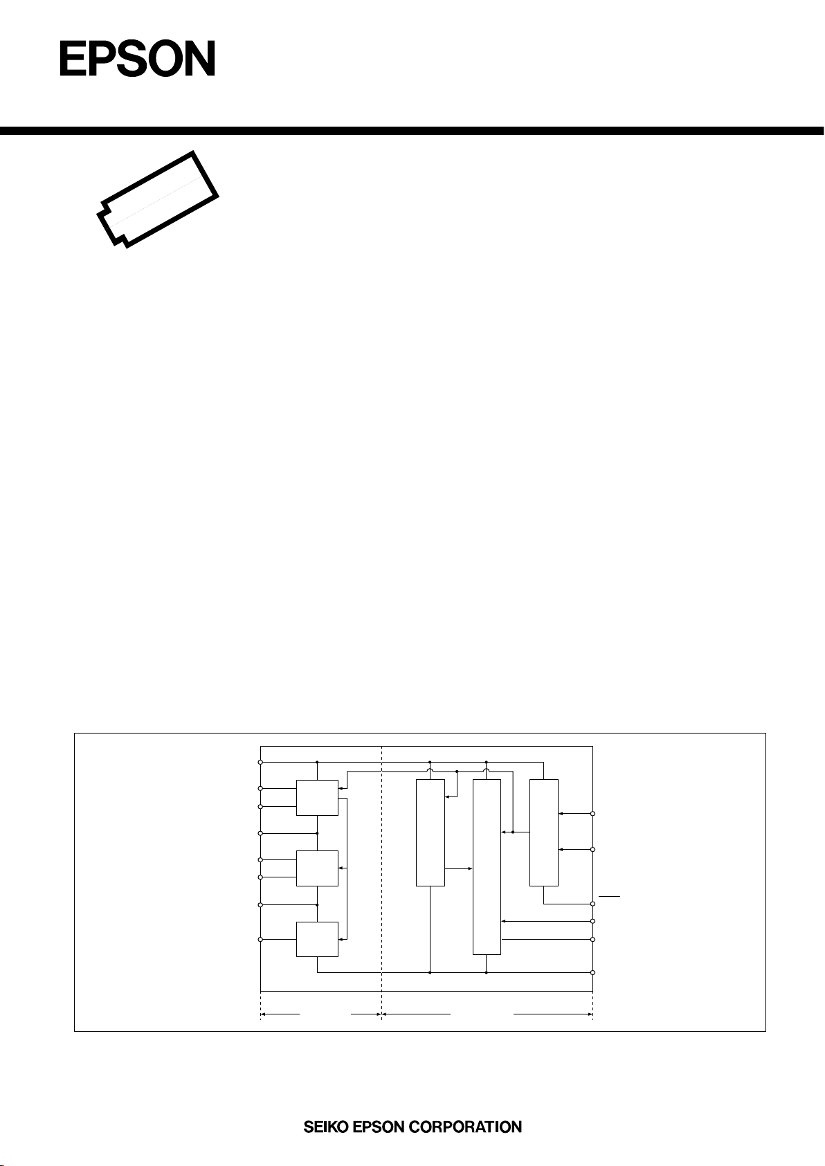
Oscillator
Voltage
Converter
(I)
Voltage
Converter
(II)
Reference Voltage
Generator
Voltage Regulator
Temperature Gradient
Select Circuit
TC1
TC2
P
off
V
reg
V
out
RV
Booster Regurator
DC-DC Converter
PF110-10
● 95% Typical Power Efficiency
● Doubled or Tripled Output Voltage
● Internal Voltage Regulator
SCI7661C
OA
/M
OA
■ DESCRIPTION
The SCI7661COA/
MOACMOS DC-DC Converter features high operational performance with low power dissipation.
It consists of two major parts: the booster circuitry and the regulator circuitry. The booster generates a doubled
output voltage (–2.4 to –12V) or tripled output voltage (–3.6 to –18V) from the input (–1.2 to –6V). The regulator is
capable of setting the output to any desired voltage. The regulated voltage can be given one of the three threshold
temperature gradients.
■ FEATURES
● High performance with low power dissipation
● Simple conversion of V
IN
(–5V) to |VIN| (+5V),
2 |VIN| (+10V), 2V
IN
(–10V) or 3V
IN
(–15V)
● On-chip output voltage regulator
● Power conversion efficiency–Typ. 95%
● Temperature gradient for LCD power supply – 0.1% / °C, 0.4%/°C or 0.6%/ °C
● Power off by external signals – Stationary current at power off – Max. 2 µA
● Cascade connection–two device connected:
VIN=–5V, V
OUT
=–20V
● On-chip C'–R oscillator
● Package .................................... SCI7661C0A: DIP-14pin (plastic)
SCI7661M0A: SOP5-14pin (plastic)
SCI7661MAA: SSOP2-16pin (plastic)
■ BLOCK DIAGRAM
Low Voltage
Operation
Products
2
SCI7661C
OA
/M
OA
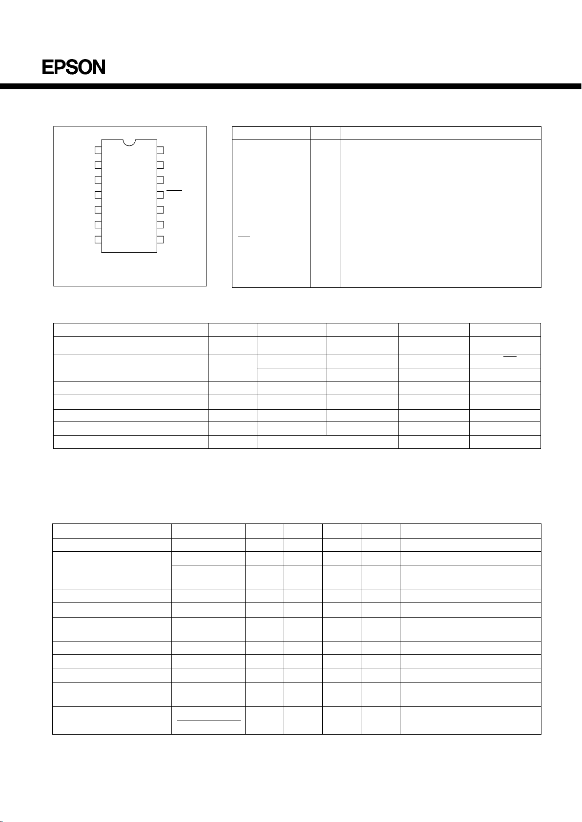
■ PIN CONFIGURATION ■ PIN DESCRIPTION
■ ELECTRICAL CHARACTERISTICS
■ ABSOLUTE MAXIMUM RATINGS
CAP1+
CAP2+
CAP1-
CAP2TC1
TC2
V
IN
1
3
2
4
5
6
7
V
DD
P
off
V
reg
V
out
OSC1
OSC2
RV
14
11
9
8
13
12
10
The same pin configuration in
DIP and SOP
CAP1+, CAP1CAP2+, CAP2TC1, TC2
V
IN
V
OUT
Vreg
R
V
P
off
OSC2, OSC1
V
DD
1, 2
3, 4
5, 6
7
8
9
10
11
12, 13
14
Pin name No. Function
Terminal for connection of capacitor for doubler
Terminal for connection of capacitor for tripler
Temperature gradient selection terminal
Power supply terminal(negative, system supply
GND)
Output terminal at tripling
Regulated voltage output terminal
Regulated voltage control terminal
Vreg output ON/OFF control terminal
Oscillation resistor connection terminal
Power supply terminal(positive system supply
VCC)
Characteristic Symbol ConditionMin. Typ. Max. Unit
(VDD = 0V, VIN=-5V, Ta=-30 to 85°C)
∆V
reg
∆V
OUT•Vreg
RL=∞, RRV=1MΩ,
V
O
=-18V
R
L
=∞, R
OSC
=1MΩ
R
L
=∞, RRV=1MΩ
V
OUT
=-15V
-18V<V
OUT
<-8V,
V
reg
=-8V, RL=∞, Ta=25°C
TC2=TC1=V
OUT
, RL=∞
R
OSC
=1MΩ
I
OUT
=10mA
V
I
V
O
-6.0
-18.0
-1.2 V
V
V
OUT
Iopr
1
-18.0
60
50
20
150
-3.2
100
V
µA
-18Vreg -2.6 V
Iopr
2
12.0 µA
I
OUT
=5mA95Peff %
0.2 %/V
I
Q
f
osc
R
OUT
16
90
2.0
24
200
µA
kHz
Ω
Input supply voltage
Output voltage
Regulator operating voltage
Booster current consumption
Regulator current
consumption
Booster power conversion
efficiency
Regulated output voltage
fluctuation
Stationary current
Oscillation frequency
Output impedance
V
I
Input terminal voltage
OSC1, P
off
TC1, TC2, RV
Plastic package
Rating Symbol Remark
V
V
Unit
0.5
0.5
Max.
V
IN
-0.5
V
OUT
-0.5
V
O
P
d
T
opr
T
stg
T
sol
Output voltage
Allowable loss
Operating temperature
Storage temperature
Soldering temperature and time
V
mW
°C
°C
-
300
85
150
-20.0
-30
-55
V
I
Input supply voltage V0.5-20/N
Min.
(VDD=0V)
260°C, 10s(at lead)
N=2 : Doubler
N
=
3 : Tripler
Note: When this IC is soldered in the solder-reflow process, be sure to maintain the reflow furnace at the curve shown in "Fig.
1-5 Reflow Furnace Temperature Curve" of this DATA BOOK. And this IC can not be exposed to high temperature of
the solder dipping.
3
SCI7661C
OA
/M
OA
■ RECOMMENDED OPERATING CONDITIONS
(V
IN
=
-
1.2V ~ -2.2V)
=C1=10µF
C
2
=10µF
+
+
+-
-
1
2
3
4
5
6
7
14
13
12
11
10
9
8
R
OSC
=
1MΩ
R
L
C
L
C
3
=22µ
F
D
1
(
V
F
(
IF=
1mA
)) ≤
0.6v
5
4
3
2
1
0
0 1.5 2 3 4 5 6
V
STA2
V
STA1
V
IN
(
V)
Triple
Double
R
L
Min.
(
k
Ω
)
Characteristic Symbol ConditionMin. Typ. Max. Unit
∆V
reg
∆I
OUT
| V
reg
(50°C) | - | V
reg
(0°C) |
50°C-0°C
CT =
1
| V
reg
(25°C) |
××100
V
OUT
=-15V, V
reg
=-8V,
Ta=25°C
0<I
OUT
<10mA, TC1=V
DD
TC2=V
OUT
R
SAT
=D(Vreg—V
OUT
)/DI
OUT
0<I
OUT
<10mA, RV=VDD,
Ta=25°C
TC2=V
OUT
, TC1=VDD, Ta=25°C
TC2=TC1=V
OUT
, Ta=25∞C
P
off
, TC1, TC2, OSC1, RV pins
Ω5
Ω5R
SAT
V
V
V
-1.5
-1.3
-0.9
-1.0
-1.1
-0.8
-2.3
-1.7
-1.1
V
RV0
V
RV1
V
RV2
%/°C
%/°C
%/°C
-0.1
-0.4
-0.6
-0.06
-0.3
-0.5
-0.25
-0.5
-0.7
CT
0
CT
4
CT
2
µA2.0I
L
Regulated output load
fluctuation
Regulated output saturation
resistance
Reference voltage
Temperature Gradient
Input leakage current
TC2=V
DD
, TC1=V
OUT
, Ta=25°C
Condition Symbol RemarkUnitMax.Min.
(Ta=-30 to 85°C)
R
OSC
=1MΩ, C
3
≥
10µF*
1
CL/C
3
≤
1/20, Ta=-20 to 85°C
R
OSC
=1MΩ
R
OSC
=1MΩ
V
V
V
Ω
mA
kHz
-2.2
2000
-1.2
20
30
-1.2
R
L
Min.*
2
10
V
STA2
V
STA1
V
STP
R
L
I
OUT
f
OSC
Booster start voltage
Booster stop voltage
Output load resistance
Output load current
Oscillation frequency
µF
3.3
C
1
, C2, C
3
kΩ680R
OSC
Capasitor for booster
Extarnal resistance for
oscillation
1000 kΩ100R
RV
Regulated output adjustable
resistance
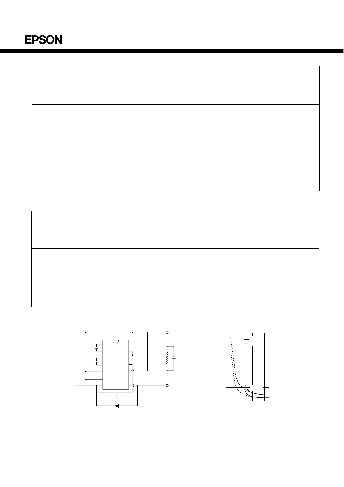
*1: Recommended circuity in low voltage operation is
shown below.
*2: R
L
Min. depends on input voltage as shown below.

4
SCI7661C
OA
/M
OA
■ PERFORMANCE CURVES
f
OSC
(kHz)
I
opr1
(µA)
f
OSC
(
kHz)
P
eff
(%)
P
eff
(%)
V
reg
(V)
I
IN
(mA)
I
IN
(mA)
P
eff
(%)
P
eff
(%)
V
OUT
(V)
R
OUT
(Ω)
R
OSC
(Ω)
I
OUT
(mA)
I
OUT
(mA) I
OUT
(mA) f
OSC
(Hz)
I
OUT
(mA)
V
IN
(V)
1000
V
OUT
(V)
0
100
90
80
70
60
50
40
30
20
10
0
100
90
80
70
60
50
40
30
20
10
0
100
90
80
70
60
50
40
30
20
10
0
100
90
80
70
60
50
40
30
20
10
0
100
90
80
70
60
50
40
30
20
10
0
40
36
32
28
24
20
16
12
8
4
0
-5
0
400
300
200
100
0
01234567
-1
-2
-3
-4
-5
-6
-10
-15
26
25
24
23
22
21
20
19
18
17
16
15
14
13
12
11
10
9
8
100
10
1
20
30
10K
–30 0
0
010
0
10
3
10
4
10
5
10
6
f
OSC
(Hz) I
OUT
(A)
10
3
10
-4
10
-3
10
-2
10
-1
I
OUT
(A)
10
-4
10
-3
10
-2
10
-1
10
4
10
5
10
6
13579246810
20 30 40 50
012345678910
10 20 30 40 50
50 100 150 0 1 2 3 4 5 6 7
100K 680K1M 10M
V
IN
=-5V
VIN=-5V
VIN=-5V
VIN=-3V
V
IN
=-3V
VIN=-1.5V
V
IN
=-1.5V
V
IN
(V)
150
100
50
Ta=25°C
Ta=25°C
VIN=-5.0V
Ta=25°C
VIN=-2.0V
Ta=25°C
V
OUT
=-15V
Ta=25°C
V
OUT
=-6V
Ta=25°C
VIN=-5V
Ta=25°C
Ta=25°C
f
OSC
=40kHz
f
OSC
=20kHz
f
OSC
=10kHz
Ta(°C)
Fig.1 Oscillation Frequency(f
OSC
)vs.
External-Resistance(R
OSC
)
Fig.4 Output Voltage(V
OUT
)vs.
Output Current(I
OUT
)
Fig.7 Power Conversion Efficiency
(P
eff
)/Input Current(IIN)vs.
Output Current(I
OUT
)
Fig.10 Power Conversion Efficiency(P
eff
)
vs.Oscillation Frequency(f
OSC
)
Fig.11 Output Voltage(V
reg
)vs. Output
Current(I
OUT
)
Fig.12 Output Voltage(V
reg
)vs. Output
Current(I
OUT
)
Fig.8 Power Conversion Efficiency
(P
eff
)/Input Current(IIN)vs.
Output Current(I
OUT
)
Fig.9 Power Conversion Efficiency
(P
eff
)vs. Oscillation Frequency
(f
OSC
)
Fig.5 Output Voltage(V
OUT
)vs.
Output Current(I
OUT
)
Fig.6 Output Inpedance(R
OUT
)vs.
Input Voltage(V
IN
)
Fig.2 Oscillation Frequency(f
OSC
)vs.
Temperature(Ta)
Fig.3 Input Voltage(VIN)vs. Booster
Current Consumption(I
opr1
)
Double
Double
P
eff
Double P
eff
Double I
IN
Double I
IN
Double
Double
Triple
Triple P
eff
Triple P
eff
Triple
Triple
Triple
I
IN
Triple I
IN
VIN=-5.0V
V
IN
=-1.5V
I
OUT
=10mA
I
OUT
=4mA
I
OUT
=20mA
I
OUT
=30mA
I
OUT
=
5mA
I
OUT
=
2mA
I
OUT
=
0.5mA
I
OUT
=
1mA
I
OUT
=
2mA
-8.000
-7.950
-7.900
-7.850
V
reg
(V)
-3.000
-2.950
-2.900
-2.850

5
SCI7661C
OA
/M
OA
■ CIRCUIT DESCRIPTION
● C-R Oscillator
The SCI7661C/M contains a C-R oscillator for internal
oscillation. It consists of an external resistor R
OSC
connected between the OSC1 pin and OSC2 pin.
● Voltage Converters
The voltage converters doubleÅ^triple the input supply voltage (VIN) using clocks generated by the C-R oscillator
●Reference Voltage Generator and Voltage Regulator
The reference voltage generator produces reference
voltage needed for operation of regulator circuit. The
voltage regulator is used to regulate a boosted output
voltage and its circuit contains a power-off function which
uses signals from the system for on-off control of the
V
reg
output.
● Temperature Gradient Selector Circut
The SCI7661C/M provides the V
reg
output with a temperature gradient suitable for LCD driving.
0.30
0.25
50
0
-50
0.20
0.15
0.10
0.05
0.00
V
OUT
=
-5V
V
OUT
=
-10V
C
T:
-0.1%/°C
C
T:
-0.4%/°C
C
T:
-0.6%/°C
V
OUT
=
-15V
I
OUT
(mA)
Ta(°C)
V
reg
(Ta) | - | V
reg
(25°C) |
0
-50 0 50 100
5101520
V
reg
-V
OUT
(V)
×
100(%)
| V
reg
(25°C) |
Fig:13 Regulated Output Saturation
Resistance(R
SAT)Vreg—VOUT
—I
OUT
Fig:14 Output Voltage(v
reg
)vs.
Temperature(Ta)
Osc1
Osc2
Osc1
Osc2
R
OSC
C-R Oscillation External Clock Operation
Open
External Clock
V
CC
VDD=0V
V
DD
=0V
V
IN
=-5V
V
IN
=-5V
CAP2=2V
IN
=-10V
V
OUT
=3VIN=-15V
(+5V)
(-5V)
GND
Typical Doubled Voltage Relations
Typical Tripled Voltage Relations
V
DD
P
off
V
reg
RV
Voltage Regulator
Control signal
R
RV
= 100kΩ to 1MΩ

6
SCI7661C
OA
/M
OA
5V
V
IN
=-5V V
OUT
=-15V
C
1
C
2
C
3
10µF
10µF
10µF
1
2
3
4
5
6
7
14
13
12
11
10
9
8
R
OSC
1MΩ
Voltage Tripler
+
+
−
+
−
–
5V
V
IN
=-5V
V
OUT
=-15V
V
reg
=-8V=
C
1
C
4
R
RV
R
1
R
RV
C
2
C
3
10µF
10µF
10µF
10µF
1
2
3
4
5
6
7
14
13
12
11
10
9
8
R
OSC
Tripler+Regulator
(-0.4%/°C selected as temperature gradient)
+
+
−
+
−
−
1MΩ
100kΩ
~1MΩ
Shield wire
R
1
R
2
V
RV
+
−
10µF
10µF
+
5V
V
IN
=-5V
V'
OUT
=-20V
V
OUT
=-10V
V'
reg
=-15V
V'
DD
=VIN=-15V
1
2
3
4
5
6
7
14
13
12
11
10
9
8
1
2
3
4
5
6
7
14
13
12
11
10
9
8
1MΩ
100kΩ
−
10µF
+
−
10µF
+
−
=VIN'
+−
10µF
+−
~
1MΩ
10µF
+
−
Serial Connection
● Temperature Gradient Assignment
1(VDD)
1
1
1
0(V
IN
)
0
0
0
P
off
L(V
OUT
)
L
H(V
DD
)
H
L
L
H
H
TC2
-0.4%/°C
-0.1%/°C
-0.6%/°C
-0.6%/°C
-
-
-
-
Temp. Gradient
ON
ON
ON
ON
OFF(Hi-Z)
OFF(Hi-Z)
OFF(Hi-Z)
OFF(Hi-Z)
V
reg
Output
ON
ON
ON
OFF
OFF
OFF
OFF
ON
CR oscillation
Cascade connection
Without regulation
Remarks
L(V
OUT
)
H(V
DD
)
L
H
L
H
L
H
TC1
Parallel Connection
5V
V
IN
=-5V
V
OUT
=-15V
V
reg
=-10V
C
4
10µF
C
3
10µF
1
2
3
4
5
6
7
14
13
12
11
10
9
8
1
2
3
4
5
6
7
14
13
12
11
10
9
8
R
OSC
C
1
C
2
10µF
10µF
+
−
+
−
+
−
C
1
C
2
10µF
10
µ
F
+
−
+
−
+
−
1MΩ
R
OSC
1MΩ
100kΩ
~1MΩ
R
RV
■ BASIC EXTERNAL CONNECTION
● Voltage Doubler and Tripler
A doubled voltage can be obtained at V
OUT
(CAP2-)
by disconnecting capacitor C2 from the tripler
configuration and shorting CAP2-- (pin4) and V
OUT
(pin 8).
● Voltage Tripler+Regulator
V
reg
output is given a temperature gradient, after
boosted output V
OUT
regulated. In this connection,
both V
OUT
and V
reg
can be taken out at the same
time.
● Parallel Connection
Parallel connection of n circuits can reduce R
OUT
to about
1/n, that output impedance R
OUT
can be reduced by
connecting serial configuraiton. A single smoothing
capacitor C3 can be used commonly for all parallely
connected circuit.
In parallely connection, a regulated output can be
obtained by applying the regulation circuit to only one of
the n parallely connected circuit.
● Cascade Connection
Cascade connection of SCI7661C/M (by connecting VIN and V
OUT
of one stage to VDD and VIN respectively of
the next stage) further increase the output voltage. Note, however, that the serial connection increases the
output impedance.
NOTE: The potential at Low level is different between the P
off
pin and the TC1/TC2 pin.

7
SCI7661C
OA
/M
OA
5V
V
IN
=
-5V
V
DD
=0V
V
OUT
=8.2V
C
1
10µF
C
2
10µF
C
3
10µF
1
2
3
4
5
6
7
14
13
12
11
10
9
8
R
OSC
+−
+−
+−
D
1
D
2
D
3
1MΩ
Positive Voltage Conversion D1, D2, D3,: Shottky
diodes with small V
F
are recommended.
5V
V
IN
=
-5V
V
OUT2
=
8.2V
V
DD
=0V
V
OUT1
=-15V
V
OUT1
=-10V
V
OUT2
=13.2V
V
DD
=5V
V
DD
=0V
10µF
10µF
10µF
10µF
1
2
3
4
5
6
7
14
13
12
11
10
9
8
++−
−
++−
+−
10µF
+−
−
1MΩ
Negative Voltage Convertion +Positive Voltage Conversion
1
2
3
4
5
6
7
14
13
12
11
10
9
8
10µF
+
−
R
1
R
RV
R
P
R
T
V
reg
V
DD
Example of Change of Temperature Gradient
Plastic DIP-14pin
Unit: mm
(inch)
14 8
17
19.7
max
(
0.775
max
)
19
±0.1
(
0.748
±0.003
)
6.3
±0.1
(
0.248
±0.003
)
1.5
(
0.059
)
0.46
±0.1
(
0.018
)
+0.004
–0.003
2.54
(
0.1
)
0°
15°
7.62
(
0.3
)
0.25
(
0.01
)
+0.001
–0
+0.03
–0.01
0.8
±0.1
(
0.031
)
+0.004
–0.003
3
min
(
0.119
min
)
4.4
±0.1
(
0.173
)
+0.004
–0.003
■ PACKAGE DIMENSIONS
● Positive Voltage Conversion
The input voltage can be doubled or tripled toward the positive
side. (In the doubler configuration, capacitor C2 and diode D
3
are disconnected and the diode D3 shorted at the both ends.)
In this case, however, the output voltage decrease by VF (forward
voltage)
For example VDD=0V, VIN=–5V and VF=0.6V, then V
OUT
=10V–
3×0.6V=8.2 V (if doubled, 5V–2×0.6V=3.8V)
● Negative Voltage Conversion + Positive
Voltage Conversion
This circuit produces outputs of –15V and +8.2V from
the –5V input. Note that this configuration causes
higher output impedance than in a single function
(negative or positive voltage converter).
● Changing the Temperature Gradient through Use of External
Temperature Sensor (Thermistor)
The SCI7661C/M has a temperature gradient selector circuit in its
regulator. It selects any one of the three gradients: –0.1% / °C, –0.4% /
°C and –0.6% / °C. It is necessary that the temperature gradient can be
changed to any other value by connecting a thermistor in series to the
output voltage control resistor RRV.

8
SCI7661C
OA
/M
OA
Plastic SOP5-14pin
Unit: mm
(inch)
814
71
INDEX
1.27
±0.1
(
0.05
±0.003
)
10.2
±0.2
(
0.402
)
5.5
±0.2
(
0.217
)
+0.007
–0.008
0.4
±0.1
(
0.016
)
+0.003
–0.004
2.2
max
(
0.086
max
)
0.15
±0.1
(
0.006
)
+0.003
–0.004
0.4
(
0.016
)
+0.007
–0.008
8
±0.3
(
0.315
±0.011
)
2.3
(
0.09
)
1.25
(
0.049
)
10.5
max
(
0.413
max
)
0.1
±0.08
(
0.004
±0.003
)

9
SCI7661C
OA
/M
OA
ELECTRONIC DEVICES MARKETING DIVISION
Electronic Device Marketing Department
IC Marketing & Engineering Group
421-8, Hino, Hino-shi, Tokyo 191-8501, JAPAN
Phone: +81-(0)42-587-5816 Fax: +81-(0)42-587-5624
ED International Marketing Department I (Europe & U.S.A.)
421-8, Hino, Hino-shi, Tokyo 191-8501, JAPAN
Phone: +81-(0)42-587-5812 Fax: +81-(0)42-587-5564
ED International Marketing Department II (Asia)
421-8, Hino, Hino-shi, Tokyo 191-8501, JAPAN
Phone: +81-(0)42-587-5814 Fax: +81-(0)42-587-5110
NOTICE
No part of this material may be reproduced or duplicated in any form or by any means without the written permission of Seiko
Epson. Seiko Epson reserves the right to make changes to this material without notice. Seiko Epson does not assume any liability
of any kind arising out of any inaccuracies contained in this material or due to its application or use in any product or circuit and,
further, there is no representation that this material is applicable to products requiring high level reliability, such as, medical
products. Moreover, no license to any intellectual property rights is granted by implication or otherwise, and there is no
representation or warranty that anything made in accordance with this material will be free from any patent or copyright
infringement of a third party. This material or portions thereof may contain technology or the subject relating to strategic products
under the control of the Foreign Exchange and Foreign Trade Control Law of Japan and may require an export license from the
Ministry of International Trade and Industry or other approval from another government agency.
All product names mentioned herein are trademarks and/or registered trademarks of their respective companies.
©Seiko Epson Corporation 1998 All rights reserved.
http:/ /www.epson.co.jp
Electric Device Information of EPSON WWW server
 Loading...