

Page 1
77
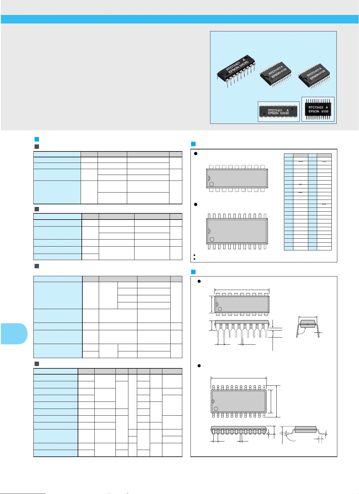
Real time clock module
Specifications (characteristics)
Absolute Max. rating
Operating range
Frequency characteristics and current consumption
characteristics
DC characteristics
External dimensions
Terminal connection
RTC-72421
(Unit: mm)
23.1 Max.
3.3 Min. 0.2 Min.
6.3
4.2
1182173164155146137128119
10
RTC72421 A
EPSON 5053C
RTC72423 A
EPSON 6150
(VDD) and VDD are to have the same level of voltage. Do not connect it to any external terminals.
NC is not connected internally.
1242233224215206197188179161015111412
13
RTC-72421
RTC-72423
RTC-72423
0.05 Min.
2.8 Max.
7.62
0.25
2.5
16.3 Max.
7.9
12.2 Max.
0.2
1.0
0.3
No.
1
2
3
4
5
6
7
8
9
10
11
12
13
14
15
16
17
18
No.
1
2
3
4
5
6
7
8
9
10
11
12
13
14
15
16
17
18
19
20
21
22
23
24
STD. P
CS
0
ALE
A
0
A
1
A
2
A
3
RD
GND
WR
D
3
D2
D1
D0
CS1
(VDD
)
(V
DD
)
VDD
72423
STD. P
CS
0
NC
ALE
A
0
NC
A
1
NC
A
2
A3
RD
GND
WR
D
3
D2
D1
NC
NC
D
0
CS1
NC
(
V
DD
)
(
V
DD
)
V
DD
72421
90° to
105°
0° to
10°
1.27 0.35
2.54 0.65 Max.
4-bit REAL TIME CLOCK MODULE
RTC-72421/72423
•
Built-in crystal unit allows adjustment-free efficient operation.
•
ALE input terminal available for 8048, 8051, and 8085 series.
•
12/24 h clock switchover function and automatic leap year setting.
•
Interrupt masking.
•
30 second adjustment function.
•
Low current consumption and features a backup function.
Item
Power source voltage
Input and output voltage
Storage temperature
Soldering condition
Symbol
V
DD
VI/O
TSTG
TSOL
Condition
Ta=+25 °C
Ta=+25 °C
RTC-72421
RTC-72423
RTC-72421
RTC-72423
Specifications
-0.3 to 7.0
GND -0.3 to V
DD+0.3
-55 to +85
-55 to +125
Under +260 °C within 10 s
(lead part) (package should
be less than +150 °C)
Twice at under +260 °C within 10
s or under +230
°
C within 3 min.
Unit
V
°C
Item
Operating voltage
Operating temperature
Data holding voltage
CSI data holding time
Operation restoring time
Symbol
V
DD
TOPR
V
DH
tCDR
tR
Condition
RTC-72421
RTC-72423
Refer to the data
holding timing
Specifications
4.5 to 5.5
-10 to 70
-40 to 85
2.0 to 5.5
2.0 Min.
Unit
V
°C
V
µs
Item
Frequency tolerance
Frequency temperature
characteristics
Aging
Shock resistance
Current consumption
Symbol
∆f/fo
fa
S.R.
I
DD1
I
DD2
Ta=+25 °C
VDD=5 V
72421 A
72421 B
72423 A
72423
Condition
Three drops on a
hard board from 750 mm
or 29400 m/s
2
x 0.3 ms x
1/2 sine wave x 3 directions
CS1=0 V
Exclude input/
output current
VDD=5 V
V
DD=2 V
Specifications
±10
±50
±20
±50
+10/-120
±5 Max.
±10 Max.
10 Max.
5 Max.
Unit
x 10
-6
x 10-6/year
x 10
-6
µA
Item
“H” input voltage (1)
“L” input voltage (1)
Input leak current (1)
Input leak current (2)
“L” output voltage (1)
“H” output voltage
“L” output voltage (2)
Off leak current
Input capacity
“H” input voltage (2)
“L” input voltage (2)
Symbol
V
IH1
VIL1
ILK1
ILK2
VOL1
VOH
VOL2
IOFFLK
C1
VIH2
VIL2
Condition
—
V1=VDD/0 V
I
OL=2.5 mA
IOH=-400 µA
IOL=2.5 mA
V1=VDD/0 V
Input
frequency 1 MHz
VDD=2 to 5.5 V
Min.
2.2
—
2.4
—
4/5 VDD
—
Typ.
—
10
20
—
Max.
—
0.8
±1
±10
0.4
—
0.4
10
—
1/5 VDD
Unit
V
µA
V
µA
pF
V
Applicable
terminal
All inputs
other than
CS
1
Input other
than D
0 to D3
D0 to D3
STD.P
Input other
than D
0 to D3
D0 to D3
CS1
-10 °C to +70 °C
(+25 °C reference temperature)
V
DD=5 V, Ta=+25 °C,
first year
Actual size
Page 2
78
Real time clock module
CS1
VIH
(
CS1
)
VIH
VIH
VIH
VIH
VIH
VIH VIH
VIL
VIL
VIL
VIH
VIL
VIL
VIL
VIH
(
CS1
)
tSU
(
CS1
)
tSU
(
A-ALE
)
tH
(
ALE-A
)
tSU
(
ALE-W
)
tSU
(
D-W
)
tSU
(
W-ALE
)
tSU
(
R-ALE
)
t
W
(
ALE
)
CS0
ALE
WR
A0 to A3
D0 to D3
tH
(
CS1
)
tH
(
W-D
)
tW
(W)
CS1
CS1
CS0 or WR not occurred
CS
1
VIH
(
CS1
)
1/5VDD
VDD
4 V 4 V
V
IH2 VIH2
VIL2 VIL2
tCDR tR
VIH
VIH
V
OH
V
OL
V
OH
V
OL
VIH
VIH VIH
VIL
VIL
VIH
VIL
VIL
VIL
VIL
VIH
(
CS1
)
tSU
(
CS1
)
tSU
(
A-ALE
)
tH
(
ALE-A
)
tSU
(
ALE-R
)
tPZV
(
R-Q
)
tPVZ
(
R-Q
)
tSU
(
R-ALE
)
trnc
(R)
t
W
(
ALE
)
CS0
ALE
RD
A
0 to A3
D0 to D3
tH
(
CS1
)
2 to 4 V
≤
Data storage mode
Interface possible
with external
terminals
Interface possible
with the external
terminals
OSC
DIVIDER
READ • WRITE
CONTROL
ADDRESS LATCH
DATA BUS • BUFFER
ADDRESS DECODER
RD WR CS1 ALE CS0 A0 D0 D1 D2 D3A1 A2 A3
STD•P
64 HZ
REST
STOP
30ADJ
BUSY
HOLD
CARRY PER
SEC.
CARRY PER
MIN.
CARRY PER
HOUR
4
4
4
4
4
IRQFLAG
24/12
Seconds Minutes Hours
Days
Months Years
Week
Sec 1 Sec 10 Min 1 Min 10 Hou 1 Hou 10 Day 1 Day 10 Mon 1 Mon 10 Yea 1 Yea 10 Reg D Reg E Reg F
Register table
Switching characteristics (with ALE
)
Read mode (with ALE
)
Write mode (with ALE
)
Data holding timing
Block diagram
(
V
DD
=
5 V ± 0.5 V
)
0=“L” level,1=“H” level, REST = RESET ITRPT/ STND=INTERRUPT/STANDARD
1) Bit does not exist.
2) Please mask AM/PM bit with 10's of hours operations.
3) Busy is read only. IRQ can only. IRQ can only be set low (“O”).
4
)
5) TEST bit should be “O”.
(
Please connect ALE to V
DD if the microprocessor does not have an ALE output.
)
∗
0
1
2
3
4
5
6
7
8
9
A
B
C
D
E
F
A3
0
0
0
0
0
0
0
0
1
1
1
1
1
1
1
1
A2
0
0
0
0
1
1
1
1
0
0
0
0
1
1
1
1
A1
0
0
1
1
0
0
1
1
0
0
1
1
0
0
1
1
A0
0
1
0
1
0
1
0
1
0
1
0
1
0
1
0
1
S
1
S10
MI 1
MI10
H 1
H10
D1
D10
MO
1
MO
10
Y1
Y10
W
Reg
D
Reg
E
Reg
F
D
3
s
8
∗
mi
8
∗
h
8
∗
d
8
∗
mo
8
∗
y
8
y80
∗
30 sec.
ADJ
t1
TEST
D
2
s
4
s40
mi4
mi
40
h4
PM/AM
d4
∗
mo
4
∗
y
4
y40
w4
IRQ
FLAG
t
0
24/12
D
1
s2
s20
mi2
mi20
h2
h20
d2
d20
mo2
∗
y
2
y20
w2
BUSY
ITRPT
/STND
STOP
D0
s1
s10
mi1
mi10
h1
h10
d1
d10
mo1
mo10
y1
y10
w1
HOLD
MASK
REST
Count
Value
0 to 9
0 to 5
0 to 9
0 to 5
0 to 9
0 to 2
or
0 to 1
0 to 9
0 to 3
0 to 9
0 to 1
0 to 9
0 to 6
-----
Remarks
1- second digit register
10- second digit register
1- minute digit register
10- minute digit register
1- hour digit register
PM/AM,10- hours digit register
1- day digit register
10 -day digit register
1- month digit register
10- month digit register
1- year digit register
10- year digit register
Week register
Control Register D
Control Register E
Control Register F
Item
CS
1 setup time
Address setup time before ALE
Address hold time after ALE
ALE pulse width
ALE setup time before WRITE
ALE setup time before READ
ALE setup time after WRITE
ALE setup time after READ
WRITE pulse width
DATA delay time after READ
DATA Hold time after READ
DATA setup time before WRITE
DATA hold time after WRITE
CS
1 hold time
READ/WRITE recovery time
Symbol
t
SU (CS1)
t
SU (A-ALE)
t
H (ALE-A)
t
W (ALE)
t
SU (ALE-W)
t
SU (ALE-R)
t
SU (W-ALE)
t
SU (R-ALE)
t
W (W)
t
PZV (R-Q)
t
PVZ (R-Q)
t
SU (D-W)
t
H (W-D)
t
H (CS1)
t
REC (R/W)
Condition
CL=150 pF
Min.
1000
50
50
80
0
0
50
50
120
---0
80
10
1000
200
Max.
----
120
70
----
Unit
ns
Address
Register
Data Bit
1
0
PM/AM
PM
AM
ITRPT/STND
ITRPT
STND
24/12
24
12
Data
 Loading...