Page 1

73
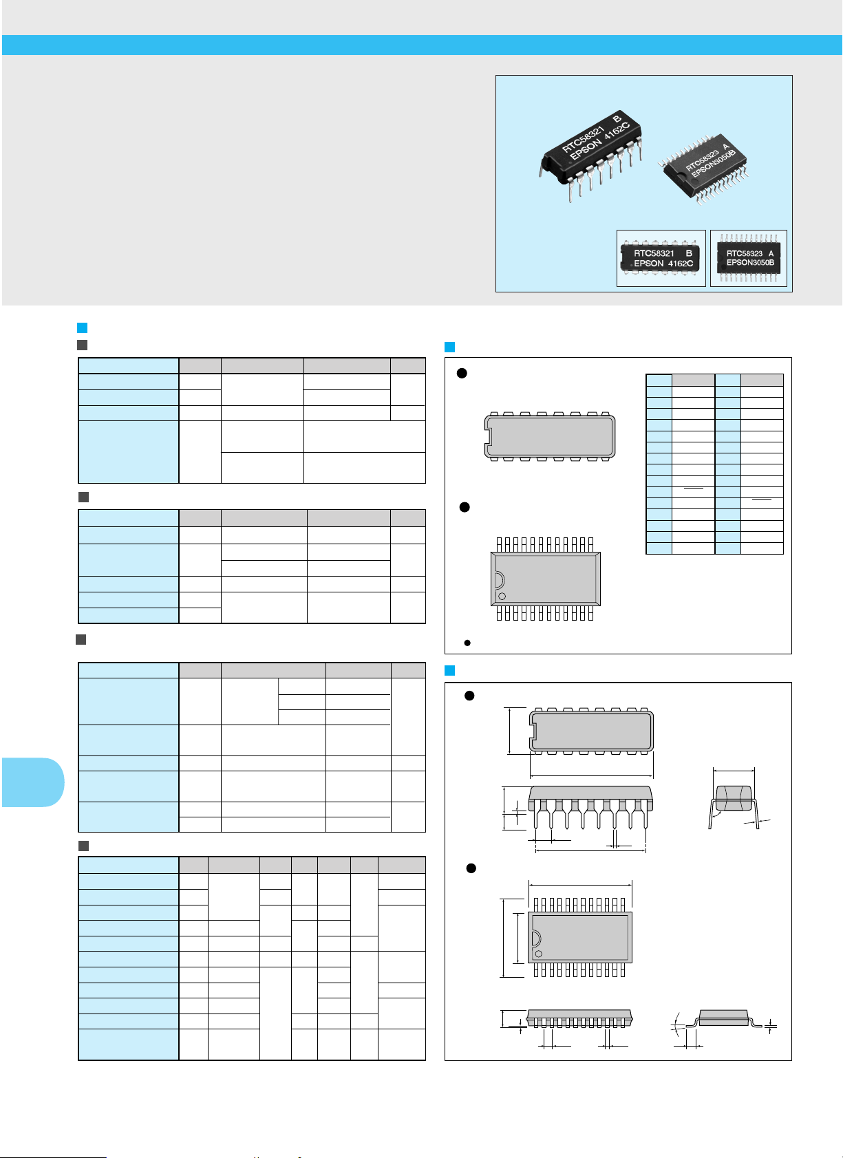
Real time clock module
Absolute Max. rating
Specifications (characteristics)
Operating range
Frequency characteristics and current consumption
characteristics
DC characteristics
External dimensions
(Unit: mm)
NC is not connected internally.
Terminal connection
0.2
1.0
0.351.27
0.5
2.54
No.
1
2
3
4
5
6
7
8
9
10
11
12
13
14 to 15
16
No.
1 to 4
5
6
7
8
9
10
11
12
13
14
15
16
17
18 to 24
58321
CS
2
WRITE
READ
D
0
D1
D2
D3
GND
ADDRESS WRITE
BUSY
STOP
TEST
CS
1
N.C
V
DD
58323
N.C
CS
2
WRITE
READ
D
0
D1
D2
D3
GND
ADDRESS WRITE
BUSY
STOP
TEST
CS
1
VDD
RTC58323 A
EPSON 3050B
0.25
6.65
4
.5 Max.
2.8 Max. 12.2 Max.
7.9
3.0 Min.
0.05 Min.
0.1 Min.
90° to
105°
7.62
20.5 Max.
16.3 Max.
17.78
RTC-58323
RTC-58323
RTC-58321
RTC-58321
24 23 22 21 20 19 18 17 16 15 14 13
123456789
10 11 12
87654321
910111213141516
0° to
10°
4162CEPSON
RTC58321 B
4-bit I/ O CONNECTION REAL TIME CLOCK MODULE
RTC-58321/58323
•
Built-in crystal unit allows adjustment-free efficient operation.
•
Incorporating time counter (hour, minute, sec.) and calendar counter
(year, month, day of week).
•
Either 12 h or 24 h selectable and leap year automatically adjustable.
•
Standard signal output selectable among a choice of 1024 Hz, 1 sec., 60
sec., and 1 hour.
•
Provided with counter start, stop and reset functions.
•
Data transmission is by 4-bit bidirectional bus line and memory read and
write method.
•
Low current consumption and backup function provided.
Item
Power source voltage
Input and output voltage
storage temperature
Soldering condition
Symbol
V
DD
VI/O
TSTG
TSOL
Condition
Ta=+25 °C
—
RTC-58321
RTC-58323
Specifications
-0.3 to 6.5
-0.3 to VDD+0.3
-55 to +85
Unit
V
°C
Under +260 °C within 10 s
(lead part) (package should
be less than +150 °C)
Twice at under +260 °C within
10 s or under +230 °C within 3
min.
Item
Operating voltage
Operating temperature
Data holding voltage
CSI data holding time
Operation restoring time
Symbol
V
DD
TOPR
V
DH
tCDR
tR
Condition
—
RTC-58321
RTC-58323
—
Refer to the data
holding timing
Specifications
4.5 to 5.5
-10 to +70
-30 to +85
2.2 to 5.5
0 Min.
Unit
V
°C
V
µs
Item
Frequency tolerance
Frequency temperature
characteristics
Aging
Shock resistance
Current consumption
Symbol
∆f/fo
—
fa
S.R.
I
DD 1
IDD 2
Condition
Ta=+25 °C
V
DD=5 V
58321 A
58321 B
58323
-10 °C to +70 °C
(+25 °C reference temperature)
VDD=5 V, Ta=+25 °C, first year
Three drops on a hard board from 750
mm or 29400 m/s2x 0.3 ms x 1/2 sine
wave x 3 directions
VDD=5 V, CS1=0 V
V
DD=3 V, CS1=0 V
Specifications
±10
±50
5±20
+10/-120
±5 Max.
±10 Max.
40 Max.
20 Max.
Unit
x 10
-6
x 10-6/year
x 10
-6
µA
Item
“H” input voltage
“H” input voltage
“L” input voltage
“L” output voltage
“L” output current
“H” input current
“L” input current
Input leak current
Input off leak current
Input capacity
Oscillation star t-up time
Symbol
VIH1
VIH2
VIL
V
OL
IOL
IIH
IIL
ILIH
ILIL
C1
tOSC
Condition
—
I
OL=1.6 mA
V
O=0.4 V
V
1=5 V
V
1=0 V
V
1=5 V
V1=0 V
Input
frequency 1 MHz
VDD=5 V
Ta=+25 °C
Min.
3.6
VDD-0.5
—
1.6
10
—
Typ.
—
—
30
—
5
1.5
Max.
—
0.8
0.4
—
80
-1
1
-1
—
3.0
Unit
V
mA
µA
pF
s
Applicable
terminal
Input other
than CS
1
CS1
—
Input other
than D
0 to D3
D0 to D3
—
Busy output
Unless otherwise stated, characteristics (specifications) shown in the above
table are based on the rated operating temperature and voltage condition.
Actual size
Page 2

74
Real time clock module
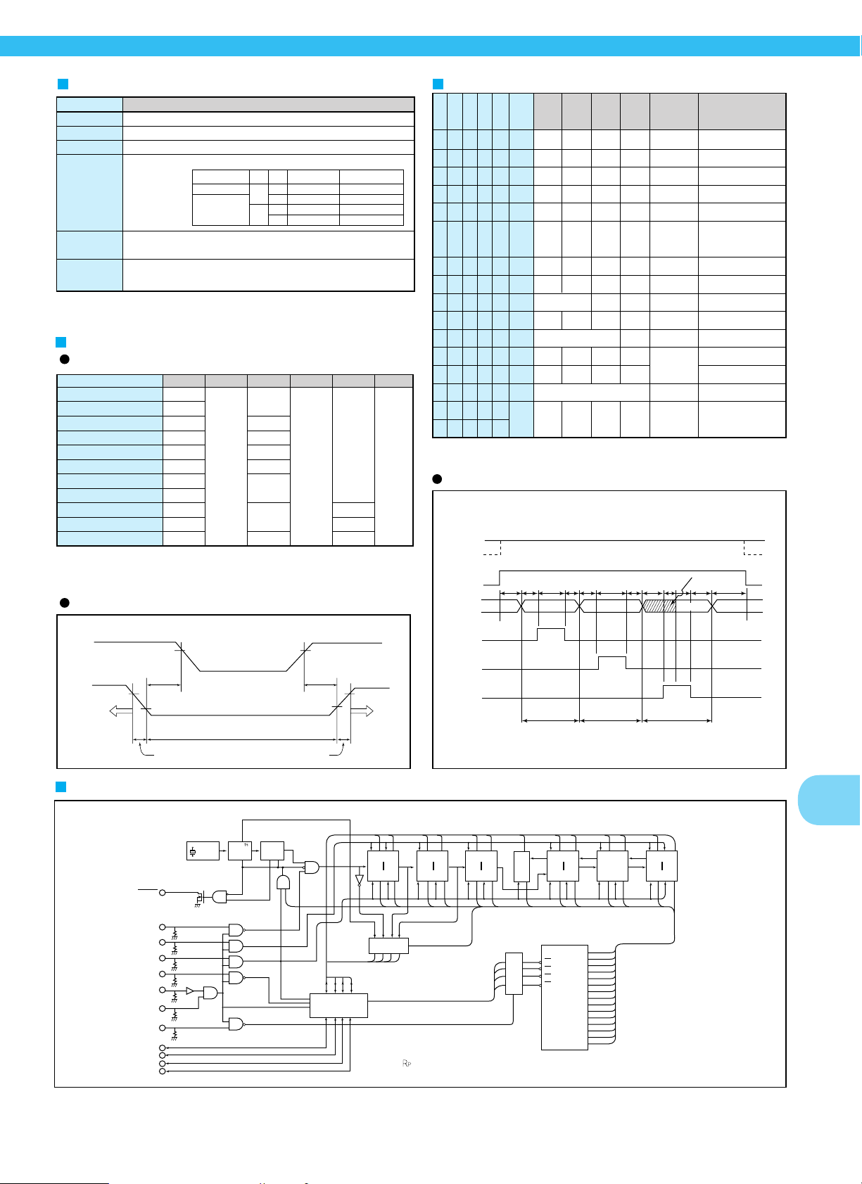
Switching characteristics
Write & read mode
Supplement Register table
CS1
CS2
tCS tAS tAW tAH tDS tWW tDH tRI tRA
tDD
DATA VALID
DATA INVALID
tCH
ADDRESS
WRITE
D
0 - D3
Write and read timing
Date holding timing
4.5 V 4.5 V
2.2 to 4.5 V
Data holding mode
CS
2 or WR not occurred
CS1 ≤ 0.8 V
0 µs Min. 0 µs Min.
t
CDR tR
VIL VIL
VIH2 VIH2
CS1
VDD
Interface
possible with
the external
terminals
Interface
possible with
the external
terminals
WRITE
WRITE READ
READ
DATA
(V
DD=5 V ±0.5 V Ta=+25 °C)
DATAADDRESS
Block diagram
OSC
TRI-STATE
CONTROL
SWITCH
DATA BUS
1024 Hz
1/2
Reg
1/3600 Hz
ADDRESS
LATCH
D
BUSY
Reg
BUSY
STOP
TEST
READ
CS
1
RP
Crystal oscillator circuit
32.768 kHz
RP
RP
RP
RP
RP
RP
CS2
D0
D1
D2
D3
ADDRESS
WRITE
WRITE
1/10
sec.
1/6 1/10
minute
1/6 1/10
day
1/3 1/10
year
1/101/12
month
1/12
hour
or
1/24
1/7
day
of
week
D10
A0
0
S1
S1
S10
S10
1/60 Hz1 Hz
1 Hz
1024 Hz
MI1
MI1 M1
TEST
WRITE
MI10
H
1
H110
H
10
H10
W
W
D1
D1
D10
D10
MO1
MO1
MO10
MOI0
Y1
Y1
Y10
Y10
D
E to F
1
2
3
4
5
6
7
8
9
A
B
C
D
A1
A2
A3
D11
D12
D13
E to F
E to F
=200 kΩ (Typ.)∗
Address
Item
∗ mark
24/12
PM/AM
D
3 and D2 of
10 days digit
Reset register
Standard
signal register
Description
Writable. Recognized as 0 while in read mode
“1” =24 h mode,“0” =12 h mode
“1” =PM, “0” =AM. In 24 h mode, this will be “0”
Used to select leap year. Calculated according to the surplus
Calendar
Gregorian calendar
Spare
D
3
0
1
D
2
0
1
0
1
Surplus after dividing
10 year digit by 4
0
3
2
1
Example of leap year
96, 00
These selections are for resetting 5-stage and the busy circuit after 1/215frequency stage.
Resetting is activated by latching this code on to the address latch and setting WRITE=H
By latching this code to the address latch and setting READ to H, the standard
signals will be output at D
0 to D
3
Note: • Do not enter erroneous data for clock.
• This may result in time keeping error.
• Do not change STOP more than once while in BUSY mode.
0
1
2
3
4
5
6
7
8
9
A
B
C
D
E
F
D
3
A3
0
0
0
0
0
0
0
0
1
1
1
1
1
1
1
1
D
2
A2
0
0
0
0
1
1
1
1
0
0
0
0
1
1
1
1
D
1
A1
0
0
1
1
0
0
1
1
0
0
1
1
0
0
1
1
D
0
A0
0
1
0
1
0
1
0
1
0
1
0
1
0
1
0
1
Name of
register
S1
S
10
MI1
MI10
H1
H10
W
D
1
D10
MO1
MO
10
Y1
Y10
—
—
D
3
S
8
∗
mi
8
∗
h
8
24/12
∗
d
8
mo8
y8
y80
1 hour
Leap year selection
D2
S
4
S40
mi4
mi40
h4
PM/AM
W
4
d
4
mo
4
y
4
y40
1 min.
D1
S
2
S20
mi2
mi20
h2
h20
W
2
d2
d20
mo2
y2
y20
1 sec.
D
0
S
1
S10
mi1
mi10
h1
h10
W
1
d1
d10
mo1
mo10
y1
y10
1024 Hz
Count
0 to 9
0 to 5
0 to 9
0 to 5
0 to 9
0 to 2
or
0 to 1
0 to 6
0 to 9
0 to 3
0 to 9
0 to 1
0 to 9
Note
1- sec. digit register
10 - sec. digit register
1 - min. digit register
10 - min. digit register
1 - hour digit register
10 - hour digit register
Week register
1 - day digit register
10 - day digit register
1- month digit register
10-month digit register
1
-
year digit register
10
-
year digit register
Reset register
Standard signal register
0== “L” level 1== “H” level
Item
CS setup time
Address setup time
Address write pulse width
Address hold time
Data setup time
Write pulse width
Data hold time
Read inhibit time
Read access time
Read delay time
CS hold time
Symbol
t
CS
tAS
tAW
tAM
tDS
t
WW
tCH
tRI
tRA
tDD
t
CH
Condition
—
Min.
0
0.5
0.1
0
2
0
—
0
Typ.
—
Max.
—
∗1
1
—
Unit.
µs
(VDD=5 V±0.5 V)
∗
1 tRA=1 µs+C x R x In [VDD/(VDD-VH)]
C: Data line capacity
R: Pull-up resistance
V
H: “
H” input voltage connected to the data line
In: Natural logarithm
after dividing
10 year digit
by 4
∗
∗
 Loading...