

Page 1

EPSON
EPSON
EPSON France S.A.
SERVICE MANUAL
GT-1200
PRODUIT
Page 2

SERVICE MANUAL
Color Image Scanner
EPSON GT-12000
4008511
®
Page 3

NOTICE
n
All rights reserved. No part of this manual may be reproduced, stored in a retrieval system, or transmitted in any form or by any means, electronic,
mechanical, photocopying, recording, or otherwise, without the prior written permission of SEIKO EPSON CORPORATION.
n
The contents of this manual are subject to change without notice.
n
All effort have been made to ensure the accuracy of the contents of this manual. However, should any errors be detected, SEIKO EPSON would greatly
appreciate being informed of them.
n
The above not withstanding SEIKO EPSON CORPORATION can assume no responsibility for any errors in this manual or the consequences thereof.
EPSON is a registered trademark of SEIKO EPSON CORPORATION.
General Notice: Other product names used herein are for identification purpose only and may be trademarks or registered trademarks of their respective
owners. EPSON disclaims any and all rights in those marks.
Copyright © 1996 SEIKO EPSON CORPORATION. Printed in Japan.
Page 4

PRECAUTIONS
Precautionary notations throughout the text are categorized relative to 1)Personal injury and 2) damage to equipment.
DANGER
Signals a precaution which, if ignored, could result in serious or fatal personal injury. Great caution should be exercised in performing
procedures preceded by DANGER Headings.
WARNING
Signals a precaution which, if ignored, could result in damage to equipment.
The precautionary measures itemized below should always be observed when performing repair/maintenance procedures.
DANGER
1. ALWAYS DISCONNECT THE PRODUCT FROM THE POWER SOURCE AND PERIPHERAL DEVICES PERFORMING ANY MAINTENANCE OR
REPAIR PROCEDURES.
2. NOWORK SHOULD BE PERFORMED ON THE UNIT BY PERSONS UNFAMILIER WITH BASIC SAFETY MEASURES AS DICTATED FOR ALL
ELECTRONICS TECHNICIANS IN THEIR LINE OF WORK.
3. WHEN PERFORMING TESTING AS DICTATED WITHIN THIS MANUAL, DO NOT CONNECT THE UNIT TO A POWER SOURCE UNTIL
INSTRUCTED TO DO SO. W HEN THE POWER SUPPLY CABLE MUST BE CONNECTED, USE EXTREME CAUTION I N WORKING ON POWER
SUPPLY AND OTHER ELECTRONIC COMPONENTS.
WARNING
1. REPAIRS ON EPSON PRODUCT SHOULD BE PERFORMED ONLY BY AN EPSON CERTIFIED REPAIR TECHNICIAN.
2. MAKE CERTAIN THAT THE SOURCE VOLTAGES IS THE SAME AS THE RATED VOLTAGE, LISTED O N THE SERIAL NUMBER/RATI NG PLATE. I F
THE EPSON PRODUCT HAS A PRIMARY AC RATING DIFFERENT FROM AVAILABLE POW ER SOURCE, DO NOT CONNECT IT T O THE POW ER
SOURCE.
3. ALWAYS VERIFY THAT T HE EPSON PRO DUCT HAS BEEN DISCO NNECT ED FROM THE PO WER SOURCE BEFORE REMOVING OR REPLACI NG
PRINTED CIRCUIT BOARDS AND/OR INDIVIDUAL CHIPS.
4. I N ORDER TO PROTECT SENSITIVE MICROPROCESSORS AND CIRCUI TRY, USE STATIC DISCHARGE EQUI PMENT, SUCH AS ANTI-STATIC
WRIST STRAPS, WHEN ACCESSING INTERNAL COMPONENTS.
5. REPLACE MALFUNCTIONING COMPONENTS ONLY WITH THOSE COMPONENTS BY THE MANUFACTURE; INTRODUCTION OF SECONDSOURCE ICs OR OTHER NONAPPROVED COMPONENTS MAY DAMAGE THE PRODUCT AND VOID ANY APPLICABLE EPSON WARRANTY.
Page 5

PREFACE
This manual describes basic functions, theory of electr ical and m echanical oper ations, maintenance and repair procedures of G T-12000. The instructions and
procedures included herein are intended for the experienced repair technicians, and attention should be g iven to the precaution s on the preceding page. T he
chapters are organized as follows:
CHAPTER 1. PRODUCT DESCRIPTIONS
Provides a general overview and specifications of the product.
CHAPTER 2. OPERATING PRINCIPLES
Describes the theory of electrical and mechanical operations of the product.
CHAPTER 3. TROUBLESHOOTING
Provides the step-by-step procedures for troubleshooting.
CHAPTER 4. DISASSEMBLY AND ASSEMBLY
Describes the step-by-step procedures for disassembling and assembling the
product.
CHAPTER 5. ADJUSTMENTS
Provides Epson-approved methods for adjustment.
CHAPTER 6. MAINTENANCE
Provides preventive maintenance procedures and the lists of Epson-approved
lubricants and adhesives required for servicing the product.
APPENDIX
Provides the following additional information for reference:
• Connector pin assignments
• Electric circuit boards components layout
• Exploded diagram
• Electrical circuit boards schematics
Page 6

REVISION STATUS
Rev. Date Page(s) Contents
A 1997/10/20 All First release
Page 7

TABLE OF CONTENTS
PRODUCT DESCRIPTIONS
1.1 OVERVIEW....................................................................................................................................................................1-1
1.2 SPECIFICATION ...........................................................................................................................................................1-1
1.3........................................................................................................................................................................................1-4
1.3 INTERFACE SPECIFICATION ......................................................................................................................................1-4
1.4 CONTROL CODE..........................................................................................................................................................1-5
1.5 OPERATION SPECIFICATIONS...................................................................................................................................1-6
1.5.1 Switch Specification...........................................................................................................................................................................1-6
1.5.2 LED Specification ...............................................................................................................................................................................1-6
1.5.3 Switch Setting.....................................................................................................................................................................................1-7
1.5.4 Error Indication...................................................................................................................................................................................1-7
1.5.5 Readable Area..................................................................................................................................................................................... 1-8
1.5.6 Transportation Screw.........................................................................................................................................................................1-8
OPERATING PRINCIPLES
2.1 GENERAL DESCRIPTION ............................................................................................................................................2-1
2.2 MECHANISM OPERATING PRINCIPLES.....................................................................................................................2-2
2.3 ELECTRICAL CIRCUIT OPERATIONS.........................................................................................................................2-3
2.3.1 Control Circuit Operation...................................................................................................................................................................2-3
2.3.2 Power Supply Circuit Operation........................................................................................................................................................2-5
Page 8

TROUBLESHOOTING
3.1 OVERVIEW....................................................................................................................................................................3-1
3.1.1 Error Detection by the Self-Diagnostic Function.............................................................................................................................3-1
3.1.2 Troubleshooting .................................................................................................................................................................................3-2
3.1.2.1 Test Points................................................................................................................................................................................3-2
3.1.2.2 Check Points for Abnormal Phenomenon.................................................................................................................................3-2
3.1.3 Troubleshooting for Electrical Circuit ..............................................................................................................................................3-8
3.1.3.1 Power Supply Board (B054PSH Board)....................................................................................................................................3-8
3.1.3.2 Control Circuit Board (B054MAIN Board)..................................................................................................................................3-9
DISASSEMBLY AND ASSEMBLY
4.1 OVERVIEW....................................................................................................................................................................4-1
4.1.1 Tools....................................................................................................................................................................................................4-1
4.1.2 Screws................................................................................................................... ..............................................................................4-1
4.2 DISASSEMBLY PROCEDURES ...................................................................................................................................4-2
4.2.1 Electrical Circuit Removal..................................................................................................................................................................4-3
4.2.1.1 EPROM Replacement...............................................................................................................................................................4-3
4.2.1.2 MAIN/B054PSH Board Removal...............................................................................................................................................4-4
4.2.2 Scanner Body Disassembly...............................................................................................................................................................4-5
4.2.2.1 Upper Housing Removal...........................................................................................................................................................4-5
4.2.2.2 Scanner Mechanism Removal .............................................................................................. ....................................................4-6
4.2.3 Scanner Mechanism Disassembly....................................................................................................................................................4-7
4.2.3.1 Panel Board Assembly Removal...............................................................................................................................................4-7
4.2.3.2 Sub Board Assembly Removal..................................................................................................................................................4-8
4.2.3.3 HP Sensor (CR) Removal.........................................................................................................................................................4-9
4.2.3.4 CR Motor Assembly Removal .................................................................................................................................................4-10
Page 9

4.2.3.5 Glass Frame Assembly Removal and Pre-operation ..............................................................................................................4-11
4.2.3.6 Lamp Assembly and Inverter Board Assembly Removal ........................................................................................................4-14
4.2.3.7 HP (AF) Sensor Removal........................................................................................................................................................4-16
4.2.3.8 AF Motor Assembly Removal.................................................................................................................................................4-17
4.2.3.9 AF Motor Assembly Installation............................................................................................................................................... 4-18
4.2.3.10 Option Frame Assembly Removal.........................................................................................................................................4-19
ADJUSTMENT
5.1 OVERVIEW....................................................................................................................................................................5-1
MAINTENANCE
6.1 OVERVIEW....................................................................................................................................................................6-1
6.1.1 Cleaning...............................................................................................................................................................................................6-1
6.1.2 Lubrication..........................................................................................................................................................................................6-1
APPENDIX
7.1 OVERVIEW....................................................................................................................................................................7-1
7.1.1 Connector Pin Assignment................................................................................................................................................................7-1
7.1.2 Connector Summary...........................................................................................................................................................................7-1
7.2 COMPONENT LAYOUT ........................................................................................................... .....................................7-6
7.3 CIRCUIT DIAGRAMS ....................................................................................................................................................7-8
7.4 EXPLODED DIAGRAMS.............................................................................................................................................7-10
Page 10

PRODUCT DESCRIPTIONS
CHAPTER
1
Page 11

GT-12000 Product Descriptions
Rev. A
1-1
1.1 OVERVIEW
The GT-12000 is an A3 size flat-bed type color image scanner. The main
features of the scanner are:
q High resolution
Optical resolution is 800 dpi.
q Wide readable area
Accommodates up to A3 size.
q High-quality image
12bit A/D input/output (optical density is 3.0.)
q High-speed scanning
Scanning A3/Portrate At 800dpi / Draft-mode;
Full-color = Approx. 15mS/line
256 Gray = Approx. 10.8mS/line
Line art = Approx. 10.8mS/line
q Adjustable Focusing function
Adjustable up to 5mm above the surface of document table.
q Quick operation
Xe-Gas Cold Cathode Fluorescent Lamp allows no initial light-up for
immediate scanning.
q New command level: ESC/I-B8 (B6 level with Focus control)
q Optional unit enhancing the function of the unit
n Transparency Unit
n Duplex scanning ADF (Automatic Document Feeder)
1.2 SPECIFICATION
GENERAL
Type: Flat-bed color image scanner
Scanning Method: Sub-Scanning mirror movement system
Photoelectric Device: Color CCD Line sensor
Color Separation: Color filter separation
Light Source: Xe-Gas Cold Cathode Fluorescent Lamp
Scanning Resolution: 800 (Main) by 800 (Sub) dpi
Output Resolution: 50 to 3200dpi (1dpi increment)
Effective Picture Element: 9760 by 13760 pixel (Max.)
Maximum Readable Area: 12.2 by 17.2 inch (310 by 437mm)
Scanning Speed: At 800 dpi / Draft mode;
Table 1-1. Scanning Speed
Original A4/Portrait A4/Portrait - A3/Portrait
Reading Area Less than 210mm 210 to 310mm
Line Art Approx. 7.5mS/line Approx. 10.8mS/line
256 Gray-scale Approx. 7.5mS/line Approx. 10.8mS/line
Full Color Approx. 10.0mS/line Approx. 15.0mS/line
Page 12

GT-12000 Product Descriptions
Rev. A
1-
2
IMAGING FUNCTIONS
Gradation: Input/internal process = 12bit/pixel
Output = 8 or 12bit/pixel
Zoom: 50 to 200% (1% increment)
Gamma Correction: CRT (A/B)
PRINTER (A/B/C)
User definable (1 level)
Color Correction: Impact-Dot Printer
Thermal Printer
Ink jet Printer
CRT Display
User definable (1 level)
Brightness Control: 7 levels
Image Processing: Bi-level= Fixed threshold
TET
Half-toning= Error diffusion (A/B/C)
Dither (Resident) (A/B/C/D)
Dither (user definable) (A/B)
Focusing: One-piece CCD/Lens movement system
INTERFACE
Standard Interface: Bi-Directional Parallel
SCSI (50/50 pin connectors)
SOFTWARE
Commend Level: ESC/I-B8 (B6 level with Focus control)
ELECTRICAL SPECIFICATION
Power supply voltage: [120 V version]
Rated voltage = AC100 - 120 V (± 10%)
[220-240 V version]
Rated voltage = AC220 - 240 V (± 10%)
Rated frequency range: 50 / 60 Hz (49.5 - 60.5 Hz)
Power consumption: Approximately 60 W (without an optional unit)
Maximum 75 W (with an optional unit)
Insulation resistance: 10 M W at 500 VDC
(between AC line and chassis)
Dielectric strength: AC 1.5 KV / minute
(between AC line and chassis)
Static electricity: Panel = 10 KV
Metal = 7 KV / 150 pF, 150 W
SAFETY, EMC
Safety regulation: UL1950 with D3
CSA C22.2 NO. 950 with D3
Low voltage directive
73/23/EEC: EN60950 (TUV)
EN60950 Nordic Deviation (NEMKO)
EMC: FCC Part15 Subpart B Class B (USA)
CSA C108.8 Class B (Canada)
AS/NZS3548 Class B
Directive 89/336/EEC: EN55022 Class B
EN61000-3-2
EN61000-3-3
EN50082-1
IEC 801-2
IEC 801-3
IEC 801-4
Page 13

GT-12000 Product Descriptions
Rev. A
1-
3
ENVIRONMENTAL CONDITIONS
Temperature: Operating = 5 to 35°C
Storage = -25 to 60°C
Humidity: Operating = 10 to 80% (no condensation)
Storage = 10 to 85% (no condensation)
RELIABILITY
Main unit: MCBF 100,000 cycle
OPERATING CONDITIONS
Dust: Ordinary office or home conditions.
(Should be kept away from extreme dust.)
Illumination: Operation under direct sunlight or near
strong light source should be avoided.
DOCUMENT
Reflective type: Smooth surface such as a printing and
photograph.
Transparency type: Reversal film, Negative film
Note: The optional transparency unit must be
used.
PHYSICAL DIMENSIONS AND WEIGHT
Dimensions: 656 (W) x 458 (D) x 170 mm (H)
(See Figure 1-1.)
Weight: Approximately 20 Kg
656mm
458mm
170mm
(6.7")
(25.8")
(18")
Figure 1-1. External Dimension of the GT-12000
Page 14

GT-12000 Product Descriptions
Rev. A
1-
4
1.3 INTERFACE SPECIFICATION
This scanner is equipped with the following interfaces:
q Bi-directional Parallel Interface
n Data: 8 bit parallel
n Handshake: BUSY, /ACK handshaking
n Signal: TTL level
n Connector: 36 pins (Amphenol)
q SCSI interface
n Function: Conforms to ANSI Standard X3.131-1986.
n Electrical specification:Conforms to ANSI Standard X3.131-1986.
(TTL compatible level)
n Connector: 50 / 50 pin (Amphenol)
n Terminator: Internal terminator
Switches between “active” and “ inactive”
n SCSI ID Set with an internal rotary switch
(Range: 0 - 7)
Page 15

GT-12000 Product Descriptions
Rev. A
1-
5
1.4 CONTROL CODE
The command level for this scanner is ESC/I-B8. The commands
supported are shown in the table below.
Table 1-2. Control Code Summary
Category Command Name Code
Execute Command Identity Request ESC I
Status Flag Request ESC F
Extended Status Flag
Request
ESC f
Parameter Request ESC S
Scanning Start ESC G
Data Format Setting Set Data Format ESC Di
Set Resolution ESC R n1 n2
Set Zooming ESC H i1 i2
Set Read Area ESC A n1 n2 n3 n4
Set Color ESC Ci
Mirroring ESC Ki
Image Setting Set Brightness ESC Li
Set Gamma Correction ESC Zi
Download Gamma Table ESC zi d0 d1 - d255
Set Sharpness ESC Qi
Image Processing Set Digital Halftoning ESC Bi
Set Auto Area
Segmentation
ESC si
Download Dither Pattern ESC b I I j d (j2)
Set Color Correction ESC Mi
Download Color Correction ESC m d1 d2 - d9
Set Threshold ESC t
Table 1-3. Control Code Summary (continued)
Category Command Name Code
Auxiliary Set Scanning Mode ESC gi
Initnialize ESC @
Set Line Counter ESC di
Control Option ESC ei
Set Focus ESC pi
Focus Position Request ESC q
Set Ratio Correction for
Main and Sub Scan
ESC Wi
Set the Film type ESC Ni
Eject Paper ESC FF
Feed Paper ESC PF
Control Normal Response ACK
Abnormal Response NACK
Abort Scanning CAN
Header STX
Page 16

GT-12000 Product Descriptions
Rev. A
1-
6
1.5 OPERATION SPECIFICATIONS
1.5.1 Switch Specification
This scanner is equipped with 4 switches. Their functions are described
below:
q “
OPERATE
“
n Turns on and off the scanner.
n Pressing this switch for power-on initializes the scanner.
q “
RESET
”
Initializes the scanner.
q
SCSI ID rotary switch
(located at the back of the scanner)
Sets the SCSI device ID for this scanner when the SCSI interface is
used to connect the scanner with the host computer.
Note: The factory default value for this scanner is “2”.
q
SCSI terminator setting switch
(located at the back of the scanner)
Alternates the internal terminator setting between “Connected” and
“Disconnected” when the SCSI interface is in use.
Note: The factory default setting for this switch is “On” (Connected).
1.5.2 LED Specification
This scanner has the following 3 LED indicators:
q
OPERATE
n
Indicates the scanner’s power On/Off status. It is on when the scanner
power is on.
q
READY
n
n Comes on when the scanner is ready to receive commands. It
flickers during scanning due to data transmission between the host
computer and the scanner.
n Indicates an error type in combination with the ERROR LED
indicator when an error has occurred.
q
ERROR
nnnn
Comes On when an error has occurred.
ERROR
READY
OPERATE RESET OPERATE
ON
OFF
SW
0
1
5
2
3
4
7
6
Figure 1-2. Buttons, Switches and LED Indicators
Page 17

GT-12000 Product Descriptions
Rev. A
1-
7
1.5.3 Switch Setting
Among the switches equipped with this scanner, SCSI switch and the
terminator switch, which are used for SCSI interface, have the following
settings:
q SCSI-ID setting switch
ID No. Availability Note
0 Available Normally assigned to other SCSI device such
as a hard disc.
1 Available Normally assigned to other SCSI device such
as a hard disc.
2 Available Set at the factory to the scanner.
3 Available
4 Available
5 Available
6 Available
7 Available Normally assigned to the SCSI host adopter.
(Blank) Not Available Not effective / Not used
*
Not Available Not effective / Not used
CHECK POINT
üüüü
Do not set the ID number that is already assigned
to other SCSI device.
q Terminator switch
Setting Note
ON Connects to the terminal resistor. /Factory default
setting
OFF Disconnects from the terminal resistor.
CHECK POINT
üüüü
Be aware that the terminator switch must be set
according to the scanner location on the “daisychain”.
1.5.4 Error Indication
When an error has occurred, the error type is indicated by the
corresponding combination of the “READY” and “ERROR” LED indicators.
Table 1-4. Error Types and Corresponding Indications
READY
n
ERROR
nnnn
Error Type
ON ON Command error
OFF Blinks Communication error
Blinks Blinks Fatal error
OFF OFF Option error
Note: The remedies for these errors are provided in Chapter 3
“Troubleshooting”.
Page 18

GT-12000 Product Descriptions
Rev. A
1-
8
1.5.5 Readable Area
The origin point for this scanner is marked at the rear left corner of the
document table viewed from the front. See Figure 1-3 for the maximum
readable area of the scanner.
310mm
437mm
2 ±1.5mm
2 ±1.5mm
2 ±1.5mm2 ±1.5mm
Sub Scan Direction
Main Scan Direction
Front
Origin Point
Maximum Readable Area
(12.2")
(17.2")
Figure 1-3. Maximum Readable Area
1.5.6 Transportation Screw
A transportation screw is attached to the left side of the scanner viewed
from the front. Fastening the screw fixes the CR to protect the scanner
from the shock while the scanner is transported or moved. Be sure to turn
the screw to the unlocking position (Described in the figure below.) before
turning the scanner power on.
Locking position set w hile
transporting/m oving the scanner.
U n lo c k in g p o s it io n s e t w h ile
the scanner is used.
Figure 1-4. Transportation Screw
Page 19

OPERATING PRINCIPLES
CHAPTER
2
Page 20

GT-12000 Operating Principles
Rev. A
2-1
2.1 GENERAL DESCRIPTION
The EPSON GT-12000 is mainly composed of the following units:
q Scanner mechanism
(Lamp/Mirror units, CR drive mechanism, integral lens/CCD sensor
unit drive mechanism)
q Control Circuit
q Power supply circuit
The EPSON flat-bed type scanners usually read images by moving the
integral CR unit which consists of the lamp, m irror, lens/CCD sensor. This
scanner, however, characteristically has the CCD sensor and the lens in
the whole unit attached onto the mechanism as an independent unit. This
scanner is also equipped with the newly designed focusing function which
enables the scanner to focus by adjusting the distance between the lens
and the CCD sensor. Therefore, the lens unit is set m ovable and driven by
the specified motor. Since the separate units in the mechanism such as
the lamp (light source) and the mirrors move at their own speed for
reading, the incident distance of the reflected light f rom the document to
the CCD sensor is kept constant.
The control circuit board and the power supply circuit board are stored in
the separate shield compartment. Since it is only connected to the
connector board in the scanner mechanism, it is removed and maintained
with ease.
B054SUB Board
CN1
CN2
CN3
CN6
CN7 CN5
CN4
B054PNL Board Motor
(for Lens Unit Drive)
Lamp/Mirror Unit
Mirror Unit
HP Sensor
(for Mirror)
Motor
(for Lamp/Mirror Drive)
Drive Wires
B054PSH Board
(Power Supply Circuit)
AC Input
SCSI
ID Switch
Terminator Switch
HP Sensor (Lens)
B054ISN Board
(CCD Sensor)
Lens Unit
(Optional)
I/F
B054MAIN Board
(Control Circuit)
SCSI
I/F
Bi-D
I/F
Document
Figure 2-1. Main mechanism Structure of the GT-12000
Page 21

GT-12000 Operating Principles
Rev. A
2-
2
2.2 MECHANISM OPERATING PRINCIPLES
Compared with other EPSON scanners, the main feature of this scanner
lies in its new optical mechanism used for reading images. Instead of the
united lamp & CCD movement system used for other scanners, this
scanner scans with the fixed CCD sensor and separate lamp and the
mirror units. Since the color CCD line sensor is used for the reading
device, only one light source is equipped and light is separated through
the RGB color filter.
As shown in Figure 2-2, the light source (high luminance cold cathode
xenon lamp), the first reflection mirror unit and the second reflection mirror
unit move independently at their own speed. Therefore the length of the
incident light reflected from the document to the CCD sensor is kept
constant. (Otherwise, excluding the fixed L1 and L2, LV1 and LV2 keep
changing to make the incident light length “L” constant.) Drive from the
stepping motor moves each mirror unit via the wires.
The CCD sensor and the lens are united into one unit, which is semi-fixed
on the base frame. For focusing function, it moves toward the optic with
the drive sent from the motor. (The focusing area with this function is from
0 to 5 mm (maximum) above from the glass surface.
x1
x2
L1
(Fixed)
Document
LV1 (Variable)
Document
Glass
L2
(Fixed)
Mirror Unit
Lamp/Mirror unit
Lens Unit
CCD Sensor
LV2 (Variable)
Figure 2-2. Optical Unit Structure
Page 22

GT-12000 Operating Principles
Rev. A
2-
3
2.3 ELECTRICAL CIRCUIT OPERATIONS
This section describes the electrical circuit of the GT-12000.
2.3.1 Control Circuit Operation
The control circuits of this scanner are:
q B054MAIN board (Main control circuit board)
q B054SUB board (Relay board)
q B054PNL board (Control panel board)
q B054ISN board (CCD sensor board located on the CR)
Among various functions controlled by B054MAIN board, the core control
circuit of the scanner, and B054ISN, process from reading image with the
CCD sensor to processing image signals is described below:
q B054ISN Board (CCD image sensor)
n Photoelectric conversion:
Converts light reflected from the document (light energy) into
electrical energy (electrical charge).
n Amplification
n A/D conversion:
Converts the image data produced in the form of analog electrical
signal into 12-bit digital data.
q B054 MAIN Board (processing image data)
ASIC (IC24) on this board manages most of the following functions:
n Shading correction:
Performs image data correction on a black and white basis.
n Numbers of image correction such as gamma correction, color
correction, halftoning correction. (They are carried out according to
the settings on the host side.)
After passed these processes, image data is finally output to the host.
CCD
CPU
IC 1 3
(H D 6413003TF)
M PX A/D
IC 2
(A D 9807)
R
G
B
12bit
IC 2 4
(M ERCURY)
IC 2 8
(GGIF)
IC 1
EPRO M (1Mbit)
IC 1 7
PSRAM (1Mbit)
Motor driver
IC 3/4/5/6
DRAM (1M x 4)
IC 7/8/9
PSRAM (1Mbit)
IC 1 8 - 2 3
DRAM (1M x 4)
IC 10/11/12
CN2
B i-D I/F
CN1/3
SCSI I/F
CN6
Option
Document
In v e r te r
B054 ISN Board
<Line C orrection
M e m o ry >
<R GB Im age M em ory>
<Buffer Memory>
TPU
ADF
<I/F C ontrol P rocessor>
<Im aging P rocessor>
Shading
G am m a Correction
Line C orrection
M ain/S ub Average
Color Correction
Sm oothing
Zoom
Bi/Q uad Form atting
TET
AAS
M irro r S h ift
Lens Shift
H P Sensor 1/2
B054 MAIN Board
Light
Quanti
t
y
Mon
i
t
or
Figure 2-3. Control Circuit Block Chart
Page 23

GT-12000 Operating Principles
Rev. A
2-
4
B054MAIN BOARD
Name Location Description
CPU
HD6413003TF
IC13 The CPU, which operates at 16 MHz,
controls this board.
ASIC
MERCURY
IC24 an image processor which controls the
followings:
· CCD
· Line correction memory
· Buffer memory
· Image processing
ASIC
CGIF
IC28 This I/F control processor controls the
followings:
· SCSI I/F
· Bi-D I/F
· Address decode
· PSRAM refresh
· Reset control
DRAM
(1MX4)
IC7-9
IC10-12
Line correction memory
Buffer memory
PSRAM (1M) IC8-23 RGB image memory
ROM (1M) IC1 Firmware memory
B054ISN BOARD
Name Location Description
CCD sensor
ILX734K
IC1 Color CCD line sensor
· Effective pixel = 10500x3 lines
· Single side reading system
· Shutter function
ADC
AD9807
IC2 A/D converter processing IC
Minimum resolution = 12 bit
B054SUB BOARD
This is a relay board, a module is in the shield compound along with the
PSB/PSE board, which connects the B054ISN in the mechanism with the
B054PNL board.
B054PNL BOARD
This board has a power switch (push-lock), RESET switch and LED
indicators (OPERATE, READY, ERROR).
Page 24

GT-12000 Operating Principles
Rev. A
2-
5
2.3.2 Power Supply Circuit Operation
Since the power supply circuit board B054PSH for this scanner meets the
universal specification, it can use the rated voltage in the range from 100V
to 240V.
The electrical circuit for the AC input part is designed on the basis of
200V line. In case the input voltage is 200V line level, the ordinary full
wave rectifying system is used. With this system, the voltage is rectified by
the diode bridge DB1 and then smoothed by the serial smoothing
capacitors C11 and C32 to produce approximately 250 VDC.
On the other hand, if the input voltage is 100V line level, the doubled
voltage rectifying system is used instead. With this system, the input AC
current is separated into the following 2 flows; the positive half cycles of
the current flow through the control IC (IC2) (from Pin 2 to Pin 3) via the
diode bridge (DB1) and the smoothing capacitor C11, and the negative
half cycles of the current, however, flow through the smoothing capacitor
(C32) and DB1 via IC2 (from Pin 3 to Pin 2). Through these flows, the
positive and negative AC current are separately charged in the smoothing
capacitors C11 and C32, respectively, and the doubled VDC
(approximately 250 VDC) equivalent to the input voltage of the 200V line
is produced. At power-on, the control circuit (IC2) is activated by the full
wave rectifying system. Then, if the input voltage is 100 VDC line level,
the system is automatically switched to the doubled voltage rectifying
system after certain period set by the circuit constant.
Except for the full wave rectifier circuit/voltage doubler rectifier circuit at
the AC input part, the normal RCC (Ringing Choke Converter) regulator
circuit is used for the rest part of the power supply circuit, and the dif f er ent
levels of VDC are distributed to corresponding mechanisms, as shown in
Table 2-1:
Table 2-1. DC Output Power
Output VDC Application
+5 V Logic power lines
+24 V q Motor drive power source
q Power source for the lamp (inverter)
+15 V +12 V production
(Power used to drive the cooling fan for the shield
compartment which stores B054 MAIN and B054PSH.)
+
+
Positive
Component
AC input
DB1
C11
C32
IC2
Negative
Component
Doubled Voltage
Output
[AC Input]
100 V = On
200 V = Off
Figure 2-4. Voltage Doubler Rectifier Circuit Operation
Page 25

TROUBLESHOOTING
CHAPTER
3
Page 26

GT-12000 Troubleshooting
Rev. A
3-1
3.1 OVERVIEW
This chapter describes the troubleshooting which enables you to solve the
problem efficiently when the scanner is operating abnormally. The
remedies for the errors detected by the self-diagnostic function and the
check point for each phenomenon are described in the following sections.
3.1.1 Error Detection by the Self-Diagnostic Function
The self-diagnostic function equipped with this scanner automatically
detects operating status of each part. The abnormal phenomenon
detected by the function and remedies are as follows:
Command Error
LED Status Cause Operation/Condition
READY
ERROR
Undefined command
is detected.
Ignores the wrong command
/parameter (No change made
for the current settings.), and
returns NACK to wait for the
next command/ parameter.
Remedy
The error is cleared by the correct command/
parameter.
Communication Error
LED Status Cause
Operation/
Condition
READY
ERROR
· Wrong procedure/operation is
detected in communication.
· In case of SCSI, communication
stops for over 30 seconds in
any phase other than bus free
phase.
The lamp goes
off and the
scanner stops
operating.
Remedy
Turn the scanner Off and back On or press the
“RESET” switch.
Fatal Error
LED Status Cause Operation/Condition
READY
ERROR
<Defect in the hardware>
· The lamp does not light.
· Scanner is turned on with
the CR unlocked.
· Other defects in the
scanner.
· The lamp goes off
and the scanner
stops operating.
· Sets the status bit
“7”.
Remedy
Turn the scanner Off and back On or press the
“RESET” switch.
Option Error
LED Status Cause Operation/Condition
READY
ERROR
<Defect in the options>
· The scanner cover is left
open.
· Paper end, etc..
Sets the status bit “7”.
Remedy
Remove the cause of the error.
CHECK POINT
üüüü
[Option Error] is detected when the option is
installed in the operative condition only.
Page 27

GT-12000 Troubleshooting
Rev. A
3-
2
3.1.2 Troubleshooting
This section provides test points for each major unit and check points for
each abnormal phenomenon.
3.1.2.1 Test Points
Test points for the motors and sensors are shown in the tables below.
Motors
q
Condition: Test the motor without any cables connected.
Motor Test Point Signal Level
Motor (for driving
the mirror)
<Cable connector>
Between Pin 1 and Pin3
Between Pin 2 and Pin 4
15.0 W
Motor (for driving
the focusing
mechanism)
<Cable connector>
Between Pin 1 and Pin3
Between Pin 2 and Pin 4
15.5 W
Sensors
q
Condition: Test with the scanner power on.
Motor Test Point Signal Level
HP sensor (Mirror)
<B054SUB board>
CN6: Pin 1 (Signal)
Pin 2 (GND)
H: In the home position
L: Off the home position
HP sensor
(Lens/CCD)
<B054SUB board>
CN4: Pin 1 (Signal)
Pin 2 (GND)
H: In the home position
L: Off the home position
CAUTION
Be careful not to short-circuit the signals while
checking them.
3.1.2.2 Check Points for Abnormal Phenomenon
See the table below which shows the abnormal phenomenon typically
occurs.
Table 3-1. Abnormal Phenomenon
Abnormal Phenomenon Description
Flowchart
to refer
The scanner doesn’t operate
at power on.
“OPERATE” LED does not
light.
3-1
“Fatal Error” is indicated and. CR does not move. 3-2
is not cleared after the
scanner is turned off and
back on
Abnormal movement of
CR, such as crashing into
the frame.
3-3
Lamp does not light. 3-4
“Communication Error” is
indicated.
Error when Bi-directional
parallel I/F is used.
3-5
Error when the SCSI is
used.
3-6
Scanned image is abnormal.
Black lines, White
banding, and so on
3-7
Check points for the major units listed for each phenomenon are shown in
the following pages.
Page 28

GT-12000 Troubleshooting
Rev. A
3-
3
Flowchart 3-1
Phenomenon: “Operate” LED does not light.
Disconnect the cables from the
connectors CN2/4/5/6/7 on the
B054MAIN board, then, with the
scanner power on, check the
connector CN 5 on the B054MAIN
board for the correct voltages shown
below:
Between Pins 1 and 4 : +24VDC
Between Pins 7 and 4 : + 5 VDC
Between Pins 9 and 10 : +15VDC
Are the
CN1 on the B054SUB
board and the shield
compartment connected
properly?
Yes
Yes
No
No
Start
Has the
fuse F1/F2 on the
B054PSH board
blown out?
Yes
No
Are the outputs all corrects?
A
Replace the B054PSH
board.
Yes
No
Connect the m properly.
Replace the
fuse. Has the fuse
blown again at turning
on the scanner?
A
Replace the B054PSH
board.
Disconnect the connector
cables from the connectors
CN2/4/5/6/7 on the B054SUB
board.
No
Yes
A
Check the following motors for
the correct res i s tance:
- Motor (for mirror) : 15.0
Ω
- Motor (for focus) : 15.5
Ω
Are the resistances correct?
Check the motor driver ICs on
the B054MAIN boar d.
<Motor (for mirror) >
Check if the resistanc e
between Pin 8/ 6 of IC4/3 and
the GND is infinitive.
<Motor(focus)>
Check if the resistanc e
between Pin 1/ 15 of IC5/6 and
the GND is infinitive.
Replace the
B054MAIN
board.
Are they correct?
Replace the
motor.
Yes
No
Replace the
B054MAIN
board.
Page 29

GT-12000 Troubleshooting
Rev. A
3-
4
Flowchart 3-2
Phenomenon: CR (Mirror/Lamp) does not move.
Start
With the scanner power On, check the
connector CN5 on the B054MAIN
board for the correct +24 VDC output
from the following :
Between Pin 1 and Pin 4 : +24 VDC
Turn th scanner off and move the CR
manually to chec k i f it move s smoothly.
Does the CR move abnomrmally?
The mechanism is
abnormal.
(Needs replacing.)
Unlock the screw.
No
Yes
No
Yes
Is the transportation
screw set to the locking
position?
Is the correct voltage output?
Replace the
B054PSH board.
A
Yes
No
No
Yes
A
Check the following motors for
the correct resistance:
- Motor (for mirro r) : 15.0
W
- Motor (for focus) : 15.5
W
Are the resistances correct?
Check the motor driver ICs on
the B054MAIN board.
<Motor (for mirror) >
Check if the resistance
between Pin 8/6 of IC4/3 and
the GND is infinitive.
<Motor(focus)>
Check if the resistance
between Pin 1/15 of IC5/6 and
the GND is infinitive.
Replace the
B054MAIN
board.
Are they correct?
Replace the
motor.
Yes
No
Replace the
B054MAIN
board.
Page 30

GT-12000 Troubleshooting
Rev. A
3-
5
Flowchart 3-3
Phenomenon: CR moves abnormally. (Crashing into the frame)
Start
Replace the HP
sensor (for mirror).
Set the screw to
the unlocking
position.
No
Yes
Check the connector CN4 on the B054
MAIN board for the HP s i
g
nal level.
Is the signal
level "HIGH" when the
CR is at the home
position?
Replace the
B054MAIN boar d.
No
Yes
Is the transportation
screw set to the lockin
g
position?
Flowchart 3-4
Phenomenon: Lamp does not light.
Start
Replace the
B054MAIN board.
Does the lamp l ight
normally?
Lamp is
defective.
No
Yes
Replace the inverter board on the CR.
Does the l amp light normally?
Inverter board
is defective.
No
Yes
Replace the lamp on the CR.
Page 31

GT-12000 Troubleshooting
Rev. A
3-
6
Flowchart 3-5
Phenomenon: “Communication Error
” (Bi-directional I/F)
” (Bi-directional I/F)” (Bi-directional I/F)
” (Bi-directional I/F)
is indicated.
Start
Repace the
B054MAIN board.
No
Yes
Replace the int erface cable.
Does the scanner
operate normally?
Replace the I/ F cable.
Flowchart 3-6
Phenomenon: “Communication Error
” (SCSI)
” (SCSI)” (SCSI)
” (SCSI)
is indicated.
Replace the
B054MAIN board.
Are the settings correct?
Set them
correctly.
No
Yes
Replace the I/F c able.
I/F cable is
defective.
No
Yes
Does the scanner
operate normally?
Start
Check the SCSI for the following
settings:
- Terminator settin
g
- SCSI ID settin
g
Page 32

GT-12000 Troubleshooting
Rev. A
3-
7
Flowchart 3-7
Phenomenon: Scanned image is abnormal.
Start
B054MAIN
board is
defective.
Clean the
glass.
No
Yes
Clean the
mirror.
No
Yes
Replace the B054MAIN board and
perform a test scannin
g
.
Is the image normal?
The mechnasim is
defective.
(Needs replacing.)
No
Is the glass free of stain
and foreign matter?
Wipe the mirror with
a dr
y
, clean cloth only.
Is the mirror free of stain
and forei
g
n matter?
Yes
Page 33

GT-12000 Troubleshooting
Rev. A
3-
8
3.1.3 Troubleshooting for Electrical Circuit
This section describes the abnormal phenomenon and corresponding
check points for each electrical circuit board.
3.1.3.1 Power Supply Board (B054PSH Board)
Phenomenon Check Points
<Abnormal voltage>
+5VDC is not output.
Check IC51 (TL494):
· Signal waveform output from
Pin 8/11 (chopping waveform)
<Abnormal voltage>
+24 VDC is not output.
Check the Switching FET/Q1:
· Waveform at the drain
<Abnormal voltage>
+15 VDC in not output.
Check IC52 (78M15):
· Signal waveform output from
Pin 1
Page 34

GT-12000 Troubleshooting
Rev. A
3-
9
3.1.3.2 Control Circuit Board (B054MAIN Board)
Phenomenon Check Points
<No operation at all>
Reset IC is defective.
Check the reset IC (IC2) for the signal
waveforms output from the following pins:
· Pin 7 (for +5V input)
· Pin 6 (for PWRES output)
<No operation at all>
ROM access is bad.
Check the CPU (IC13) for the ROM
access signal waveforms output from the
following pins:
· Pin 104 (for CS0 signal)
· Pin 78 (for RD signal)
<No operation at all>
CPU is defective.
Check the clock signal waveform input to
the following pin:
· Pin 75 (for XTAL input)
Page 35

GT-12000 Troubleshooting
Rev. A
3-1
0
Phenomenon Check Points
<”Fatal Error”>
Motor (for mirror) driver circuit
is defective.
Check the Driver IC (IC3/4:
· Phase drive signal waveform
output from Pin 8/6
<”Fatal Error”>
Motor (for focus) driver circuit
is defective.
Check the driver IC (IC5/6):
· Phase drive signal waveform
output from Pin 1/15
<”Fatal Error”>
CR does not stop at the home
position.
· Check if the signal waveform
input to Pin 91 of CPU (IC13)
changes in accordance with the
CR position.
<”Fatal Error”>
Lamp does not light.
Check the following for the lamp
signal output:
· Output from Pin 166 of ASIC
(IC24)
· Emitter waveform at Tr (Q1)
<”Fatal Error”>
White standard level is not
read properly.
Check ASIC (IC28):
· Signal waveform output from
Pin 161
<”Communication Error”>
Bi-directional I/F / SCSI I/F
Main cause: ASIC (IC28) is
defective. (Replace IC28 or
B054MAIN board.)
<Image is read abnormally> Main cause: ASIC (IC24) is
defective. (Replace IC24 or
B054MAIN board.)
Page 36

DISASSEMBLY AND ASSEMBLY
CHAPTER
4
Page 37

GT-12000 Disassembly and Assembly
Rev. A
4-1
4.1 OVERVIEW
This chapter describes how to disassemble this scanner. Unless otherwise
specified, assembly can be accomplished by following disassembly
procedures in reverse order.
WARNING
n
n n
n Be sure to disconnect the power cable from the
AC power socket prior to servicing.
n
n n
n Since this scanner weighs heavy
(approximately 20 Kg), it must be carried by
2 people.
CAUTION
n
n n
n Never disassemble any scanner parts unless
specified to do so, because this scanner
mechanism needs assembling and adjusting
rather exactly to preserve accurate control
system at its satisfactory level.
n
n n
n Get yourself enough room for servicing,
considering the size of the scanner.
n
n n
n Since this scanner weighs as heavy as
approximately 20 kg, be sure to perform
servicing on a heavy-duty, level table.
n
n n
n Make sure that the “CR fixing knob” is set to
the locking position to fix the CR by the rear
before packing the scanner.
4.1.1 Tools
Tools used for servicing are as listed in the table below:
Table 4-1 .Tool List
Description Availability SE Part No.
Exclusive adjusting tools
(Leveling tools)
EPSON exclusive Code: 1039140
Phillips screw driver (No.2)
¡
–
Standard screw driver (No.1)
¡
–
Tweezers
¡
–
4.1.2 Screws
Screws used in this scanner are listed in the table below. Be sure to use
the correct types and numbers of screws for each part when assembling
the scanner.
Table 4-2. Screw List
No.
Screw Type /
Specification
Appearance Color
1 CBP M4x12 Silver
2 CB M4x10 Gold
3 CBS M3x6 Red copper
4 CB M3x4 Gold
5 CBP M3x8 Gold
6 CB M3x6 Gold
7 CB M3x12 Black
8
CR;B damper shaft
(Thread part: M3x3)
Gold
9 CP M3x6 Silver
10
Screw lock screw
(Diagonal: 5 mm)
Silver
Page 38

GT-12000 Disassembly and Assembly
Rev. A
4-
2
4.2 DISASSEMBLY PROCEDURES
This section describes disassembling and removing procedures for each
major unit of the scanner.
See the flowchart in Figure 4-1. The jobs in the yellow boxes involve using
the adjustment tools exclusively designed for this scanner. Therefore,
make sure that you read the instruction for the section to refer to carefully
to figure out the procedure before servicing.
Start
Electrical Circuit
Remova
(Section 4.2.1)
EPROM Replacement
(Section 4.2.1.1)
MAIN/Power Supply Board
Removal (Section 4.2.1.2)
Scanner Body
Disassembly
(Section 4.2.2)
Upper Housing Removal
(Section 4.2.2.1)
Mechanism Removal
(Section 4.2.2.2)
Panel Board Assembly Removal
(Section 4.2.3.1)
Sub Board Assembly Remvo al
(Section 4.2.3.2)
HP Sensor (CR) Removal
(Section 4.2.3.3)
Motor (CR) Assembly Removal
(Section 4.2.3.4)
Glass Frame Assembly Removal
(Section 4.2.3.5)
Scanner Mechanism
Dsassembly
(Section 4.2.3)
Lamp/Inverter Board Assembly
Removal (Section 4.2.3.6)
HP Sensor (AF)
Removal (Section 4.2.3.7)
Option Frame Assembly
Removal (Section 4.2.3.9)
Figure 4-1. Procedure for Disassembling the GT-12000
Page 39

GT-12000 Disassembly and Assembly
Rev. A
4-
3
4.2.1 Electrical Circuit Removal
The major electrical circuit boards (B054MAIN and B054PSH) of this
scanner are all stored in one independent shield compartment. Therefore,
they can be removed in one unit (board unit) from the scanner with ease.
1. Disconnect the AC power cable from the scanner.
2. Remove 3 screws (No.5) securing the shield compartment which
contains the electrical circuit boards at the back of the scanner. Then
take out the compartment from the scanner to remove.
CHECK POINT
üüüü
For easy removal, insert a driver or equivalent
into the bail lock of the interface and pull it.
4.2.1.1 EPROM Replacement
In case of EPROM replacement, remove the ROM cover attached on the
board unit.
1. Remove the board unit. (See Section 4.2.1.)
2. Remove 1 screw (No.3) fixing the ROM cover, and remove the cover.
3. Remove the EPROM from the IC socket and install a new EPROM.
CAUTION
When installing the ROM, make sure that the leads
are not bent and the ROM is installed in the right
direction.
S c re w (N o .5 )
Take out
Figure 4-2. Shield Compartment Removal
Screw (No.3)
ROM Cover
Figure 4-3. ROM Cover Removal
Page 40

GT-12000 Disassembly and Assembly
Rev. A
4-
4
4.2.1.2 MAIN/B054PSH Board Removal
B054MAIN and B054PSH boards stored in the shield compartment are
removed in the following procedure:
1. Remove the shield compartment. (See Section 4.2.1.)
2. Remove 12 screws (No.3) securing the top shield of the board unit,
then remove the top shield.
3.
[MAIN board assembly removal]
Disconnect the connector cables from the connector CN5 and CN9 on
the MAIN board.
4. Remove the following screws securing the MAIN board, and remove
the MAIN board:
Ÿ
6 screws (No.3): Fixing the board along the edges.
Ÿ
6 screws (No. 9): Securing the I/F connector.
Ÿ 2 screws (No.10): Securing the optional I/F connector.
.
5.
[Power supply board assembly removal]
Remove the connector cables from the connector CN1 on the power
supply board assembly
and the connector CN5 on the MAIN board
assembly.
6. Remove 6 screws (No.3) securing the power supply board assembly
and remove the power supply board.
S c re w (N o .9 )
Screw Lock Screw
(N o.10)
Figure 4-4. I/F Connector Fixing Screw Removal
Connector (CN5) Connector (CN9)
Screws (No.3)
B054MAIN Board
Figure 4-5. MAIN Board Removal
Connector (CN5)
Screws (No.3)
Connector (CN1)
B054PSH Bo a r d
Figure 4-6. Power Supply Board Removal
Page 41

GT-12000 Disassembly and Assembly
Rev. A
4-
5
4.2.2 Scanner Body Disassembly
This section describes procedures for disassembling the major units of the
scanner.
CAUTION
When removing the CR fixing knob or screw caps,
be careful not to damage the upper housing.
4.2.2.1 Upper Housing Removal
1. Remove the document cover.
2. Using tweezers, remove the CR fixing knob attached to the left side of
the scanner.
3. Remove 4 screws (2 for each of No1 and No.2) securing the upper
housing to the chassises on the scanner. Note that the front 2 screws
are covered with the screw caps. Using tweezers, pinch them out prior
to removing the screws.
4. Lift up the upper housing to remove it.
CHECK POINT
üüüü
When installing the upper housing, make sure
that the optical plate is installed on the specified
position.
Optical Plate
Inner S ide of the
Upper Housing
Screw Cap
Be careful not to dam age
the upper housing.
C ro ss-se ctio n
U sing the tw eezers, rem ove the cap
by lifting it up w hile pushing it tow ard
the other side of the cutout.
Figure 4-7. Screw Cap Removal
S c re w s (N o .1 )
Screw Cap
C R Fixing Knob
Screw Cap
S c re w s (N o .2 )
Figure 4-8. Upper Housing Removal
Page 42

GT-12000 Disassembly and Assembly
Rev. A
4-
6
4.2.2.2 Scanner Mechanism Removal
The scanner mechanism can be removed from the lower housing in the
following procedure:
1. Remove the upper housing. (See Section 4.2.2.1.)
2. Remove 4 screws (No.1) securing the scanner mechanism to the lower
housing at the bottom. Then remove the mechanism from the lower
housing.
CHECK POINT
üüüü
n
n n
n Note the following when installing the scanner
mechanism:
1) Remove the key tops for the power switch
and reset switches from the lower housing.
2) Install the scanner mechanism to the lower
housing.
3) Reinstall the key tops.
n
n n
n Place the removed mechanism on flat stable
surface.
Screws (No.1)
Front Side of the Scanner
Scanner Me chanism
Figure 4-9. Scanner Mechanism Removal
Page 43

GT-12000 Disassembly and Assembly
Rev. A
4-
7
4.2.3 Scanner Mechanism Disassembly
The rest part of the chapter describes the procedures for removing the
major parts/units in the scanner mechanism.
CAUTION
Note that producing this scanner requires rather
precise assembly and adjustment to ensure
accurate control system. Therefore, never
disassemble any scanner parts unless specified to
do so.
4.2.3.1 Panel Board Assembly Removal
1. Remove the scanner mechanism. (See Section 4.2.2.2.)
2. Turn the mechanism over and place it on a flat surface.
3. Disconnect all connector cables from the panel board assembly.
4. Remove 2 screws (No.6) securing the panel board assembly and
remove it.
CHECK POINT
üüüü
Unit arrangement at the bottom of the mechanism
is as shown below.
Motor (CR)
HP Sensor (CR)
Panel Board Assembly
Sub Board Assembly
HP Sensor (AF)
Screws (No.6)
Panel Board Assembly
Figure 4-10. Panel Board Assembly Removal
Page 44

GT-12000 Disassembly and Assembly
Rev. A
4-
8
4.2.3.2 Sub Board Assembly Removal
1. Remove the scanner mechanism. (See Section 4.2.2.2.)
2. Turn the mechanism over and place it on a flat surface.
3. Disconnect all connector cables from the sub board assembly
(B054SUB board).
4. Remove 2 screws (No.3) securing the board to the br acket and r emove
the sub board.
CHECK POINT
üüüü
When placing the scanner up side down, lay a
clean soft cloth under the scanner to protect the
glass surface.
Screws (No.6)
Sub Board Assembly
Figure 4-11. Sub Board Assembly Removal
Page 45

GT-12000 Disassembly and Assembly
Rev. A
4-
9
4.2.3.3 HP Sensor (CR) Removal
This section describes procedure for removing the HP sensor which
detects the reference position for the carriage mirror assembly.
1. Remove the scanner mechanism. (See Section 4.2.2.2.)
2. Move the carriage mirror assembly away from the HP (home position).
3. Turn the mechanism over and place it on a flat surface.
4. Release the hook fixing the HP sensor at the bottom of the mechanism
and remove the HP sensor unit. Then disconnect the connect or cable
from the removed HP sensor.
HP Sensor (AF)
Sub Board Assembly
Panel Board AssemblyHP Sensor (CR)
Motor (CR)
Figure 4-12. HP Sensor (CR) Removal
Page 46

GT-12000 Disassembly and Assembly
Rev. A
4-1
0
4.2.3.4 CR Motor Assembly Removal
This section describes procedure for removing the motor unit which drives
the carriage mechanism (mirror/lamp).
1. Remove the scanner mechanism. (See Section 4.2.2.2.)
2. Turn the mechanism over and place it on a flat surface.
3. Unhook the torsion spring from the tension lever assembly, then
remove 1 screw (No.6) to remove the tension lever assembly.
4. Disconnect the cable for the motor from the relay connector and
remove 4 CR damper shafts; B (No.8) securing the motor, then remove
the motor.
CHECK POINT
üüüü
When assembling, hook the spring to the tension
lever assembly first, then fasten the screw.
Screw (No.6)
CR Damper Shafts ;B
(No.8)
Torsion Sprin
g
Tension Lever Assembly
Motor (CR) As s emb ly
Bottom of the Scanner Facing Upward
Figure 4-13. CR Motor Assembly Removal
Page 47

GT-12000 Disassembly and Assembly
Rev. A
4-11
4.2.3.5 Glass Frame Assembly Removal and Pre-operation
Since the glass frame assembly is one of the reinforcing parts of the
mechanism, whole mechanism may be deformed if it is removed. Be sure
to follow the instruction provided in this section during any service which
involves removing the glass frame assembly.
CAUTION
Be aware the following when removing the
document glass during any service:
n
n n
n Always set the scanner on the adjusting tools
exclusively designed for this scanner.
n
n n
n Set the scanner on a stable, level table.
n
n n
n Make sure that the scanner mechanism is
installed to the lower housing while servicing.
n
n n
n Be sure to fit all the rubber foot at the bottom
of the scanner in the top indents of the stages
and the adjuster. (Any of the foot must not be
placed over the top surface of the tool.)
1. Remove the upper housing. (See Section 4.2.2.1.)
2. Refer to the figures in the right column and set the adjusting tools
(leveling tools) under the scanner to level the scanner, as instructed
below:
1) Set the scanner on 3 stages, making each of the specified feet of
the scanner sit on the corresponding stage.
2) Set the adjuster under the rubber foot in the front right corner of the
scanner bottom, aligning the center of the adjuster with the one of
the rubber foot. Make sure that you can see the groove on the
adjuster when it is set.
3) Hold the base of the adjuster with a hand and spin the table to
make it reach the bottom of the scanner by its own forth.
4) Turn the table
[2 quarters]
manually, which can be measured by 4
divisions on the table and the groove on the base, to push the table
up from the position where the table was moved up to by the spin.
5) After adjusting, make sure that each corner of the scanner is
securely in contact with the corresponding tool.
Note: Directions are described when the scanner is viewed from the front.
<Continued to the next page.>
Stage
(3 pieces)
Adjuster
Turning Table
(w ith 4 devisions)
Base
(w it h1 groove)
Figure 4-14. Adjusting Tools
Stage
(S et in the front left, rear
right and rear left coners.)
Adjuster
(S et in the front
right coner.)
Turn the turning table
to m o v e th e ta b le u p
and dow n to adjust
height.
Figure 4-15. Tool Position and Adjusting Method
Page 48

GT-12000 Disassembly and Assembly
Rev. A
4-1
2
3. Remove 9 screws and remove the glass frame assembly. The screws
to be removed and their locations are as follows:
· No.4: 5 screws securing the glass frame assembly by the right
and left sides.
· No.1: 2 screws securing the glass frame assembly by the rear
edge.
· No.3: 2 screws securing the glass frame assembly by the front
edge.
Note: Directions are described when the scanner is viewed from
the front.
CAUTION
When reinstalling the glass frame assembly, refer
to Section 4.2.3.5.1 to set the glass frame assembly
on the correct position. Failure in this operation
will cause the CR to start scanning at a wrong
position.
Screws (No.1)
Screws
(No.4)
Screws (No.3)
Front Side of the Scanner
Glass Frame Assembly
Screws
(No.4)
Glass Fixing Plate
(Color : Silve)
Glass Fixing Plate
(Color : Silve)
Figure 4-16. Glass Frame Assembly Removal
Page 49

GT-12000 Disassembly and Assembly
Rev. A
4-1
3
4.2.3.5.1 Glass Frame Assembly Installation
After the glass frame assembly has been removed for any purpose, it
must be reinstalled in the following procedure.
1. Place the glass frame assembly to the specified position in the scanner
mechanism.
2. Referring to the Figure 4-17, determine the installation position for the
glass frame assembly.
1) Push the whole glass frame assembly from the front against the
positioning bushes (color: silver) on the top side of the rear frame.
(Glass edge is in contact with the bushes with this operation.)
2) Keeping the glass frame assembly in contact with the bushes, move
the assembly left to push it against the positioning bump on the top
surface of the left side frame.
3. When the glass frame assembly is correctly positioned, fix it with 9
screws.
CHECK POINT
üüüü
When installing the glass frame assembly, ensure
that 4 glass fixing plates are properly positioned.
(See Figure 4-16.)
G lass Fram e A ssem bly
Scanner Front S ide
G lass edge
Positioning Bush
(C olor: S ilver)
Fram e P ositioning
Bum p
Figure 4-17.
Determining the Glass Frame Assembling Installation position
Page 50

GT-12000 Disassembly and Assembly
Rev. A
4-1
4
4.2.3.6 Lamp Assembly and Inverter Board Assembly Removal
This section describes how to remove the lamp assembly and the inverter
board assembly from the carriage.
1. Remove the glass frame assembly. (See Section 4.2.3.5.)
2. Move the CR to the position indicated in Figure 4-19. (The position
where the front and rear frames are indented.)
3. Remove 2 screws (No.6) securing the carriage mirror cover and slide
the cover toward the rear side of the scanner to release the
engagement with the hook on the carriage. Then lift up the cover and
remove it.
<Continued to the following page.>
Screws (No.6)
CR Mirror Cover
Figure 4-18. CR Mirror Cover Removal
Page 51

GT-12000 Disassembly and Assembly
Rev. A
4-1
5
4. Disconnect the connector cable for the lamp from the connector CN2
on the inverter board assembly. Then remove the lamp from the
carriage.
5. Disconnect the cable (black) from the connector CN1 on the inverter
board assembly. Then remove the bracket (silver) fixing the ferrite core.
6. Remove 2 screws (No.6) securing the inverter board assembly.
7. Slide the inverter board assembly toward the front side of the scanner
to release the engagement with the hook on the carriage. Then remove
the inverter board.
CHECK POINT
üüüü
When assembling, make sure that the cover is
securely engaged with the hook on the carriage.
Hook
Cover
C arriage Base
Rear
Front
Lift up to remove.
Cut Part
of the Board
Screws (No.6)
Lamp
Inverter Board
CN1
CN2
Figure 4-19.
Lamp Assembly and Inverter Board Assembly Removal
Page 52

GT-12000 Disassembly and Assembly
Rev. A
4-1
6
4.2.3.7 HP (AF) Sensor Removal
This section describes the procedure for removing the HP sensor which
detects the reference position for the AF drive mechanism (lens/CCD
sensor unit).
1. Remove the glass frame assembly. (See Section 4.2.3.5.)
2. Remove 4 screws (No.3) securing the AF drive mechanism cover which
covers the AF drive mechanism and remove the cover.
3. Rotate the screw pulley at the end of the screw shaft (a thread shaf t)
manually to move the detection flag to the area where it does not
overlap with the HP sensor.
4. Release the hook fixing the HP sensor and remove it, then disconnect
the cable from the sensor.
Screws (No.3)
Cover
Figure 4-20. AF Drive Mechanism Cover Removal
Rotate this pulley manually.
HP Sensor (AF)
Detection Flag
Figure 4-21. HP Sensor (AF) Removal
Page 53

GT-12000 Disassembly and Assembly
Rev. A
4-1
7
4.2.3.8 AF Motor Assembly Removal
This section describes how to remove the motor which drives AF drive
mechanism.
1. Remove the glass frame assembly. (See Section 4.2.3.5.)
2. Remove 4 screws (No.3) and remove the cover which covers the AF
drive mechanism.
3. Remove 2 screws (No.6) and remove the tension plate assembly,
spring plate and fixing tension plate to loosen the timing belt.
4. Disconnect the cable for the motor from the relay connector, then
remove 4 screws (No.4) securing the motor and remove the motor.
Screws (No.6)
Tension Plate Assembly
Fixing Tension Plate
Spring Plate
Figure 4-22. Tension Plate Assembly Removal
Screws (No.4)
Motor Assembly (AF)
Figure 4-23. AF Motor Assembly Removal
CAUTION
You are required to set the timing belt with a
special care while installing the AF motor
assembly. Be sure to follow the instruction
provided in the next page to set the timing belt
peoperly.
Page 54

GT-12000 Disassembly and Assembly
Rev. A
4-1
8
4.2.3.9 AF Motor Assembly Installation
Follow the steps below when installing the AF motor assembly to the
scanner body.
1. Engaging the timing belt with the pinion gear of the motor, install the
motor to the frame with 2 screws (No. 4).
2. Mount the sprint plate, fixing tension plate, and the tension plate
assembly, and fix them with 2 screws (No. 6) temporarily. Ensure that
the tension plate assembly is upheld by this operation.
3. Turning the screw pulley attached to the screw shaft end manually,
loosen the screw fixing the tension plate assembly to tense the belt,
then fasten the screw again.
CAUTION
When fixing the tension plate assembly, be careful
not to apply excessive tension, since it may cause
the motor to rotate improperly.
Fixing Tension Plate
Spring Plate
Tension Plate A ssem bly
Screws
(N o. 6)
Figure 4-24. Tension Plate Assembly
CHECK POINT
üüüü
When installing the tension plate assembly, make
sure that the location bump is not covered with the
plate.
Tension Plate A ssem bly
Screw Pulley
(rotated counterclockwise)
Figure 4-25. Timing Belt Tension
Page 55

ADJUSTMENT
CHAPTER
5
Page 56

GT-12000 Adjustment
Rev. A
5-1
5.1 OVERVIEW
This scanner requires no adjustment for any service such as
disassembling and assembling the scanner including part replacement is
provided within the specification in Chapter 4 “Disassemble and
Assembly”.
Page 57

MAINTENANCE
CHAPTER
6
Page 58

GT-12000 Maintenance
Rev. A
6-1
6.1 OVERVIEW
This chapter provides information necessary to keep the scanner function
in optimum condition constantly and to prevent troubles.
6.1.1 Cleaning
Perform cleaning when stain is noticeable. Stain on the document glass,
particularly, has direct effect on scanned image. Therefore, be sure to
clean the glass well to remove stain thoroughly.
CAUTION
Never apply any organic solvent such as thinner
and benzine , since these may deteriorate plastic
and rubber parts.
q Outer cases
Wipe stain off with a clean cloth which is moistened with water and
then squeezed tightly. To remove severe stain, use neutral detergent.
q Document glass
Remove dust and paper debris with a dry clean cloth. If stain is severe
or foreign matter is stuck, use a cloth absorbed with neutral detergent.
If trace is left, wipe it off well with a dry, clean cloth again.
CAUTION
If you need to clean the reverse side of the glass,
be sure to remove the glass using the specified
adjusting tools.
6.1.2 Lubrication
This scanner needs no lubrication at the level of service specified in the
service manual.
Page 59

APPENDIX
CHAPTER
7
Page 60

GT-12000 Appendix
Rev. A
7-1
7.1 OVERVIEW
This chapter provides information necessary for servicing.
7.1.1 Connector Pin Assignment
CN3
CN2 CN4 CN7
CN5
CN6
CN1
CN5
CN4
CN1
CN2
CN2 CN1
CN3 CN6
Scanner M echanism
B054M A IN Board
B054P S H Board
SCSI I/F SCSI I/F
O p tio n a l I/F
AC Input
Bi-directional
I/F
B054S U B Board
B054PN L
Board
H P S ensor
(M irro r)
Motor
(M irro r)
Motor
(A F )
H P S ensor
(A F )
B054IS N
Board
Figure 7-1. Connector Pin Assignment
7.1.2 Connector Summary
Connectors used on the electrical circuit boards are summarized in the
table below.
Table 7-1. Connector Summary
Board
CN
No.
Function Ref.
B054MAIN CN1/3 For connection with SCSI I/F GT-9500
CN2 For connection with Bi-directional I/F GT-9500
CN4
For connection with B054SUB Board
(In a card-edge format)
Page 7-2
CN5
Power supply line from the B054PSH
board
Page 7-3
CN6 For connection with the option Page 7-3
B054PSH CN1 For connection with AC inlet –
CN2
ðPower supply line for B054MAIN
board
Page 7-3
B054SUB
CN1
ðFor connection to B054MAIN
board
Page 7-2
CN2
ðFor connection to B054ISN board
(CCD sensor, Inverter board)
Page 7-4
CN3 ðFor connection to B054PNL board Page 7-4
CN4
ðFor connection to the HP sensor
(for focus)
Page 7-4
CN5
ðFor connection to the motor
(for mirror)
Page 7-4
CN6
ðFor connection to HP sensor
(for mirror)
Page 7-5
CN7
ðFor connection to the motor
(for focus)
Page 7-5
Page 61

GT-12000 Appendix
Rev. A
7-
2
B054MAIN – CN4
No. Signal Name Function
A1 GND GND
A2 GND GND
A3 ADD2 Address (2)
A4 ADD0 Address (0)
A5 A/D AD clock
A6 WR WR signal for ADC
A7 CLP Clamp signal for ADC
A8 SG Shutter (Green) for CCD
A9 RSP Reset signal for CCD
A10 TG Shift signal for CCD
A11 AD1 Image data (1) after AD conversion
A12 AD3 Image data (3) after AD conversion
A13 AD5 Image data (5) after AD conversion
A14 AD7 Image data (7) after AD conversion
A15 AD9 Image data (9) after AD conversion
A16 AD11 Image data (11) after AD conversion
A17 GND GND
A18 RESETSW Reset SW signal
A19 LED(R) LED (READY) signal
A20 +5 Power supply (+5V)
A21 GND GND
A22 LAMP Lamp signal
A23 +24 Power supply (+24V)
A24 GND GND
A25 HMF(P) Home sensor (AF) (Power supply)
A26 MFA Motor (AF) (Phase A)
A27 MFAX Motor (AF) (Phase /A)
A28 HMM(S) Home sensor (Mirror) (Signal)
A29 MMB Motor (Mirror) (Phase B)
A30 MMBX Motor (Mirror) (Phase /B)
A31 GND GND
No. Signal Name Function
B1 +5V Power supply (+5V)
B2 +12V Power supply (+12V)
B3 ADD1 Address (1)
B4 STLN Start line signal for ADC
B5 CSAP Chip select ADC
B6 SMP Sample hold signal for ADC
B7 SB Shutter (Blue) for CCD
B8 SR Shutter (Red) for CCD
B9 CK Clock signal for CCD
B10 AD0 Image data (0) after AD conversion
B11 AD2 Image data (2) after AD conversion
B12 AD4 Image data (4) after AD conversion
B13 AD6 Image data (6) after AD conversion
B14 AD8 Image data (8) after AD conversion
B15 AD10 Image data (10) after AD conversion
B16 GND GND
B17 POWERSW Power switch (secondary side)
B18 LED(P) LED (POWER)
B19 LED(ER) LED (ERROR)
B20 GND GND
B21 GND GND
B22 +24 Power supply (+24V)
B23 +24 Power supply (+24V)
B24 HMF(S) Home sensor (AF) (Signal)
B25 MFB Motor (AF) (Phase B)
B26 MFBX Motor (AF) (Phase /B)
B27 GND GND
B28 HMM(P) Home sensor (Mirror) (Power supply)
B29 MMA Motor (Mirror) (Phase A)
B30 MMAX Motor (Mirror) (Phase /A)
B31 GND GND
Page 62

GT-12000 Appendix
Rev. A
7-
3
B054MAIN – CN5
No. Signal Name Function
1 +24V Power supply (for motor drive, lamp)
2 +24V Power supply (for motor drive, lamp)
3 +24V Power supply (for motor drive, lamp)
4 GND GND
5 GND GND
6 GND GND
7 +5V Power supply (for logic line)
8 +5V Power supply (for logic line)
9 +15V Power supply (for producing +12V)
10 GND GND
11 TMP Output from the thermistor
12 SW Power switch (Secondary side) control signal
B054MAIN – CN6
No. Signal Name Function
1 IN1 TPU (HOME) / Select
2 IN2 TPU (COVER) / Select
3 IN3 Not used.
4 OU5 Lamp control signal
5 IN4 Not used.
6 +5 Power supply (+5V)
7 GND GND
8 +24 Power supply (+24V)
9 SDAT Motor drive serial data for TPU
10 SCK Transfer clock for TPU
11 LOD Latch pulse for TPU
12 SEL Select signal for TPU
13 +5 Power supply (+5V)
14 GND GND
15 +24 Power supply (+24V)
16 +24 Power supply (+24V)
17 GND GND
18 +5 Power supply (+5V)
19 +5 Power supply (+5V)
20 +24 Power supply (+24V)
21 RXD RXD signal for ADF
22 /RXD /RXD signal for ADF
23 /TXD /TXD signal for ADF
24 TXD TXD signal for ADF
25 DSR DSR signal for ADF
26 DTR DTR signal for ADF
Page 63

GT-12000 Appendix
Rev. A
7-
4
B054SUB – CN2
No. Signal Name Function
1 +12 Power supply (+12V)
2 GND GND
3 +5 Power supply (+5V)
4 GND GND
5 +5 Power supply (+5V)
6 GND GND
7 +12V Power supply (+12V)
8 S2 Address (2)
9 S1 Address (1)
10 S0 Address (0)
11 STL Start line for ADC
12 A/D AD clock
13 CS Chip select signal
14 WR WR signal for ADC
15 SMP Sample hold signal for ADC
16 CLP Clamp signal for ADC
17 SB Shutter signal (Blue) for CCD
18 SG Shutter signal (Green) for CCD
19 SR Shutter signal (Red) for CCD
20 RSP Reset signal for CCD
21 CK Clock signal for CCD
22 TG Shift signal for CCD
23 AD0 Image data (0) after AD conversion
24 AD1 Image data (1) after AD conversion
25 AD2 Image data (2) after AD conversion
26 AD3 Image data (3) after AD conversion
27 AD4 Image data (4) after AD conversion
28 AD5 Image data (5) after AD conversion
29 AD6 Image data (6) after AD conversion
30 AD7 Image data (7) after AD conversion
31 AD8 Image data (8) after AD conversion
32 AD9 Image data (9) after AD conversion
33 AD10 Image data (10) after AD conversion
34 AD11 Image data (11) after AD conversion
35 GND GND
B054SUB – CN3
No. Signal Name Function
1 +24 Power supply (+24V)
2 +24 Power supply (+24V)
3 +24 Power supply (+24V)
4 +24 Power supply (+24V)
5 LAMP Lamp signal
6 GND GND
7 GND GND
8 GND GND
9 GND GND
10 +5V Power supply (+5V)
11 LED (ERR) LED (ERROR)
12 LED (RES) LED (READY)
13 LED (POW) LED (POWER)
14 RESETSW RESET switch signal
15 POWERSW POWER switch signal
16 GND GND
B054SUB – CN4
No. Signal Name Function
1 HMF(S) Home sensor (AF) (Signal)
2 GND GND
3 HMF(P) Home sensor (AF) (Power supply)
B054SUB – CN5
No. Signal Name Function
1 MFB Motor (AF) (Phase B drive signal)
2 MFA Motor (AF) (Phase A drive signal)
3 MFBX Motor (AF) (Phase /B drive signal)
4 MFAX Motor (AF) (Phase /A drive signal)
Page 64

GT-12000 Appendix
Rev. A
7-
5
B054SUB – CN6
No. Signal Name Function
1 HMM(S) Home sensor (Mirror) (Signal)
2 GND GND
3 HMM(P) Home sensor (Mirror) (Power supply)
B054SUB – CN7
No. Signal Name Function
1 MMB Motor (Mirror) (Phase B drive signal)
2 MMA Motor (Mirror) (Phase A drive signal)
3 MMBX Motor (Mirror) (Phase /B drive signal)
4 MMAX Motor (Mirror) (Phase /A drive signal)
Page 65

GT-12000 Appendix
Rev. A
7-
6
7.2 COMPONENT LAYOUT
Figure 7-2. Component Layout - B054MAIN Board
Page 66

GT-12000 Appendix
Rev. A
7-
7
Figure 7-3. Component Layout - B054PSH Board
Page 67
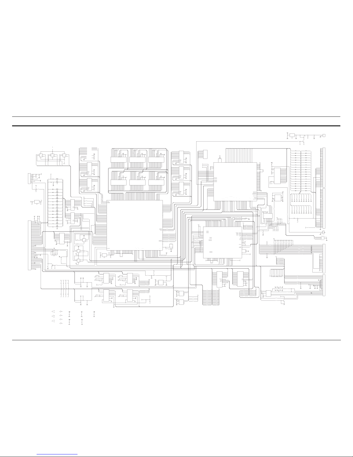
GT-12000 Appendix
Rev. A
7-
8
7.3 CIRCUIT DIAGRAMS
1
2
3
4
5
6
7
8
9
10
TP5
DIRECT
I
3O1
G
N
D
2
SR3
78M12
R208
1K
R209
4.7K
R210
1K
1
2
3
Q2
C4116
C75
0.1U
C77
0.1U
Q3
2SJ191
B16 BLM 121
C70
10U/16V
B46 BLM121
1
2
3
4
5
6
7
8
9
10
11
12
13
14
15
16
17
18
19
20
21
22
23
24
25
26
27
28
29
30
31
32
33
34
35
36
37
38
39
40
41
42
43
44
45
46
47
48
49
50
CN3
SCSI
1
2
CN9
FAN
C76
0.1U
SD0
SD1
SD2
SD3
SD4
SD5
SD6
SD7
SDP
SATN
SBSY
C22
0.1U
VDD
13
VDD
14
GND
7
VM
24
NC
1
NC
25
SL1
8
SL2
9
SL3
10
SL4
11
SL5
12
SL6
15
SL7
16
SL8
17
SL9
18
SL10
19
SL11
20
SL12
21
SL13
22
SL14
23
SL15
3
SL16
4
SL17
5
SL18
6
EN
2
IC1 6
BH9595FP
D1
RB160L
B17 BLM 121
B18 BLM 121
B19 BLM 121
B20 BLM 121
B21 BLM 121
B22 BLM 121
B23 BLM 121
B24 BLM 121
B25 BLM 121
B26 BLM 121
B28 BLM 121
B29 BLM 121
B27 BLM 121
B47 BLM121
B48 BLM 121
B49 BLM121
B50 BLM121
B51 BLM121
B52 BLM121
B53 BLM121
B54 BLM121
B55 BLM121
B56 BLM121
B57 BLM121
B58 BLM121
B59 BLM121
GIO
GCD
GMSG
GACK
GREQ
GBSY
GSEL
GDP
GD7
GD6
GD5
GD4
GD3
GD2
GD1
GD0
GD0
GD1
GD2
GD3
GD4
GD5
GD6
GD7
GDP
GSEL
GBSY
GREQ
GACK
GMSG
FD0
FD1
FD2
FD3
FD4
FD5
FD6
FD7
FDP
FSEL
FBSY
FREQ
FACK
FMSG
FD0
FD1
FD2
FD3
FD4
FD5
FD6
FD7
FDP
FSEL
FBSY
FREQ
FACK
FMSG SMSG
SACK
SREQ
SBSY
SSEL
SDP
SD7
SD6
SD5
SD4
SD3
SD2
SD1
SD0
C25
2.2U
C53
2.2U
G
D
5
G
D
4
G
D
3
G
D
2
G
D
1
G
D
0
G
C
D
G
I
O
G
S
E
L
G
B
S
Y
G
R
E
Q
G
A
C
K
G
M
S
G
G
A
T
N
G
R
S
T
123
CR3
20MHz
1
TP4
DRMER
1
TP3
BRCPU
1
TP2
DRCPU
VDD
17
VDD
32
VDD
49
VDD
62
VDD
81
VDD
97
VSS
87
VSS
85
VSS
83
VSS
80
VSS
78
VSS
76
VSS
16
VSS
33
VSS
48
VSS
56
VSS
61
VSS
64
VSS
66
VSS
68
VSS
70
VSS
72
VSS
74
BDDRQ
28
DM6
37
DM7
36
BDDAK
30
DRMER
29
BRCPU
35
DRCPU
31
I
N
T
I
F
1
0
6
EOLID2
104
LODID3
105
S
C
K
I
1
0
1
T
X
D
1
0
9
S
C
K
O
1
0
8
SH3
115
SH2
114
SH1
111
SH0
110
RWID0
102
RESI
34
NMI
116
A0
11
A1
10
A2
9
A3
8
A4
7
A5
6
A6
5
A7
4
AH
22
D
0
2
1
D
1
2
0
D
2
1
9
D
3
1
8
D
4
1
5
D
5
1
4
D
6
1
3
D
7
1
2
C
S
2
3
R
D
2
4
W
R
2
5
A
S
2
6
C
S
M
E
R
2
7
C
S
R
O
M
I
1
2
3
C
S
R
A
M
I
1
2
2
C
S
R
A
M
O
1
1
9
O
E
R
A
M
O
1
1
8
S
T
R
B
5
8
D
I
R
I
5
7
ITID 1
103
B
U
S
Y
5
9
A
C
K
6
0
P
7
4
4
P
6
4
5
P
5
4
6
P
4
4
7
P
3
5
0
P
2
5
1
P
1
5
2
P
0
5
3
C
S
A
P
1
2
6
RESMR
117
DM0
43
DM1
42
DM2
41
DM3
40
DM4
39
DM5
38
A8
3
A9
2
D
B
P
6
5
D
B
7
6
7
D
B
6
6
9
D
B
5
7
1
D
B
4
7
3
D
B
3
7
5
D
B
2
7
7
D
B
1
7
9
D
B
0
8
2
S
E
L
8
4
B
S
Y
8
6
R
E
Q
8
8
A
C
K
9
0
M
S
G
1
9
2
C
/
D
9
4
I
/
O
9
6
A
T
N
9
9
R
S
T
6
3
X
I
N
1
X
O
U
T
1
2
8
IDSEL
107
D
P
R
T
5
4
MINTEST
55
VDD
113
VDD
124
TEST1
120
TEST2
121
MONIT1
127
VSS
89
VSS
91
VSS
93
VSS
95
VSS
98
VSS
100
VSS
112
VSS
125
IC2 8
GGIF
IFD 7
IFD 6
IFD 5
IFD 4
IFD 3
IFD 2
IFD 1
IFD 0
IFD A
IFD R
G
D
P
G
D
7
G
D
6
DRMER
IFD 7
IFD 6
IFD 5
IFD 4
IFD 3
IFD 2
IFD 1
IFD 0
IFD A
IFD R
A0
9
A1
10
A2
11
A3
12
A4
14
A5
15
A6
16
A7
17
A8
18
RAS
4
CAS
23
WE
3
OE
22
D0
1
D1
2
D2
24
D3
25
VCC
13
GND
26
A9
5
IC1 0
DRAM1M*4
A0
9
A1
10
A2
11
A3
12
A4
14
A5
15
A6
16
A7
17
A8
18
RAS
4
CAS
23
WE
3
OE
22
D0
1
D1
2
D2
24
D3
25
VCC
13
GND
26
A9
5
IC1 1
DRAM1M*4
C30
0.1U
C34
0.1U
C35
0.1U
A
0
1
2
A
1
1
1
A
2
1
0
A
3
9
A
4
8
A
5
7
A
6
6
A
7
5
A
8
2
7
A
9
2
6
A
1
0
2
3
A
1
1
2
5
A
1
2
4
A
1
3
2
8
A
1
4
3
D
0
1
3
D
1
1
4
D
2
1
5
D
3
1
7
D
4
1
8
D
5
1
9
D
6
2
0
D
7
2
1
C
E
2
3
0
O
E
2
4
W
E
2
9
V
D
D
3
2
G
N
D
1
6
A
1
5
3
1
A
1
6
2
C
E
1
2
2
R
F
S
H
1
IC2 3
PSRAM128K*8
C33
0.1U
A
0
1
2
A
1
1
1
A
2
1
0
A
3
9
A
4
8
A
5
7
A
6
6
A
7
5
A
8
2
7
A
9
2
6
A
1
0
2
3
A
1
1
2
5
A
1
2
4
A
1
3
2
8
A
1
4
3
D
0
1
3
D
1
1
4
D
2
1
5
D
3
1
7
D
4
1
8
D
5
1
9
D
6
2
0
D
7
2
1
C
E
2
3
0
O
E
2
4
W
E
2
9
V
D
D
3
2
G
N
D
1
6
A
1
5
3
1
A
1
6
2
C
E
1
2
2
R
F
S
H
1
IC2 0
PSRAM128K*8
R224
47K
R225
47K
R226
47K
R227
47K
M
C
E
M
C
E
M
O
E
M
O
E
BRW
BCAS
BRAS
BRW
BCAS
BRAS
MBA9
MBA8
MBA7
MBA6
MBA5
MBA4
MBA3
MBA2
MBA1
MBA0
MBA9
MBA8
MBA7
MBA6
MBA5
MBA4
MBA3
MBA2
MBA1
MBA0 M BD0
MBD1
MBD2
MBD3
MBD4
MBD5
MBD6
MBD7
M
A
0
M
A
1
M
A
2
M
A
3
M
A
4
M
A
5
M
A
6
M
A
7
M
A
8
M
A
9
M
A
1
0
M
A
1
1
M
A
1
2
M
A
1
3
M
A
1
4
M
A
1
5
M
A
1
6
M
3
D
0
M
3
D
1
M
3
D
2
M
3
D
3
M
3
D
4
M
3
D
5
M
3
D
6
M
3
D
7
M
3
D
8
M
3
D
9
M
3
D
1
0
M
3
D
1
1
M
W
E
3
M
W
E
3
C28
0.1U
C29
0.1U
A
0
1
2
A
1
1
1
A
2
1
0
A
3
9
A
4
8
A
5
7
A
6
6
A
7
5
A
8
2
7
A
9
2
6
A
1
0
2
3
A
1
1
2
5
A
1
2
4
A
1
3
2
8
A
1
4
3
D
0
1
3
D
1
1
4
D
2
1
5
D
3
1
7
D
4
1
8
D
5
1
9
D
6
2
0
D
7
2
1
C
E
2
3
0
O
E
2
4
W
E
2
9
V
D
D
3
2
G
N
D
1
6
A
1
5
3
1
A
1
6
2
C
E
1
2
2
R
F
S
H
1
IC2 1
PSRAM128K*8
A
0
1
2
A
1
1
1
A
2
1
0
A
3
9
A
4
8
A
5
7
A
6
6
A
7
5
A
8
2
7
A
9
2
6
A
1
0
2
3
A
1
1
2
5
A
1
2
4
A
1
3
2
8
A
1
4
3
D
0
1
3
D
1
1
4
D
2
1
5
D
3
1
7
D
4
1
8
D
5
1
9
D
6
2
0
D
7
2
1
C
E
2
3
0
O
E
2
4
W
E
2
9
V
D
D
3
2
G
N
D
1
6
A
1
5
3
1
A
1
6
2
C
E
1
2
2
R
F
S
H
1
IC2 2
PSRAM128K*8
C32
0.1U
C31
0.1U
A
0
1
2
A
1
1
1
A
2
1
0
A
3
9
A
4
8
A
5
7
A
6
6
A
7
5
A
8
2
7
A
9
2
6
A
1
0
2
3
A
1
1
2
5
A
1
2
4
A
1
3
2
8
A
1
4
3
D
0
1
3
D
1
1
4
D
2
1
5
D
3
1
7
D
4
1
8
D
5
1
9
D
6
2
0
D
7
2
1
C
E
2
3
0
O
E
2
4
W
E
2
9
V
D
D
3
2
G
N
D
1
6
A
1
5
3
1
A
1
6
2
C
E
1
2
2
R
F
S
H
1
IC1 8
PSRAM128K*8
A
0
1
2
A
1
1
1
A
2
1
0
A
3
9
A
4
8
A
5
7
A
6
6
A
7
5
A
8
2
7
A
9
2
6
A
1
0
2
3
A
1
1
2
5
A
1
2
4
A
1
3
2
8
A
1
4
3
D
0
1
3
D
1
1
4
D
2
1
5
D
3
1
7
D
4
1
8
D
5
1
9
D
6
2
0
D
7
2
1
C
E
2
3
0
O
E
2
4
W
E
2
9
V
D
D
3
2
G
N
D
1
6
A
1
5
3
1
A
1
6
2
C
E
1
2
2
R
F
S
H
1
IC1 9
PSRAM128K*8
R217
47K
R218
47K
R220
47K
R221
47K
R222
47K
R223
47K
R219
47K
R216
47K
M
C
E
M
C
E
M
C
E
M
C
E
M
O
E
M
O
E
M
O
E
M
O
E
M
A
0
M
A
1
M
A
2
M
A
3
M
A
4
M
A
5
M
A
6
M
A
7
M
A
8
M
A
9
M
A
1
0
M
A
1
1
M
A
1
2
M
A
1
3
M
A
1
4
M
A
1
5
M
A
1
6
M
A
0
M
A
1
M
A
2
M
A
3
M
A
4
M
A
5
M
A
6
M
A
7
M
A
8
M
A
9
M
A
1
0
M
A
1
1
M
A
1
2
M
A
1
3
M
A
1
4
M
A
1
5
M
A
1
6
M
1
D
0
M
1
D
1
M
1
D
2
M
1
D
3
M
1
D
4
M
1
D
5
M
1
D
6
M
1
D
7
M
1
D
8
M
1
D
9
M
1
D
1
0
M
1
D
1
1
M
2
D
8
M
2
D
9
M
2
D
1
0
M
2
D
1
1
M
2
D
0
M
2
D
1
M
2
D
2
M
2
D
3
M
2
D
4
M
2
D
5
M
2
D
6
M
2
D
7
M
W
E
1
M
W
E
1
M
W
E
2
M
W
E
2
A0
9
A1
10
A2
11
A3
12
A4
14
A5
15
A6
16
A7
17
A8
18
RAS
4
CAS
23
WE
3
OE
22
D0
1
D1
2
D2
24
D3
25
VCC
13
GND
26
A9
5
IC7
DRAM1M*4
A0
9
A1
10
A2
11
A3
12
A4
14
A5
15
A6
16
A7
17
A8
18
RAS
4
CAS
23
WE
3
OE
22
D0
1
D1
2
D2
24
D3
25
VCC
13
GND
26
A9
5
IC9
DRAM1M*4
C37
0.1U
C38
0.1U
LRW
LCAS
LRAS
LCAS
LRAS
LRW
MLA3
MLA2
MLA1
MLA0
MLA9
MLA8
MLA7
MLA6
MLA5
MLA4
MLA3
MLA2
MLA1
MLA0
MLA9
MLA8
MLA7
MLA6
MLA5
MLA4
MLD4
MLD5
MLD6
MLD7
MLD8
MLD9
MLD10
MLD11
Q
S
T
B
1
2
3
4
5
6
7
8
9
10
11
12
CN5
POWER
1 3
2
FL1
NF101
1 3
2
FL2 NF101
R278
47K
1
TP1
TG
C40
100U/35V
C1
0.1U
B1
102
B2
102
D
12Q 9
C
1
3
P
1
0
CK
11
Q
8
IC3 6 B
74F74
D
2Q 5
C
1
P
4
CK
3
Q
6
IC4 0 A
74F74
D
12Q 9
C
1
3
P
1
0
CK
11
Q
8
IC4 0 B
74F74
TG SHF
S
T
R
S
T
G
S
T
B
Q
S
T
R
Q
S
T
G
M
X
1
I3O
1
G
N
D
2
SR2
78M12
C73
100U/35V
C74
100U/35V
R211
4.7K
R212
10K
C78
0.1U
1 3
2
FL3 NF101
1 3
2
FL4
NF101
1 3
2
FL5 NF101
1 3
2
FL6 NF101
1 3
2
FL7
NF101
1 3
2
FL8 NF101
1 3
2
FL9 N F101
1 3
2
FL10 N F101
B3
102
B4
102
B5
102
B6
102
B7
102
B8
102
B9
102
B10
102
C121
330P
SFR
SFG
SFB
CLPF
SFH
WRAD
CSAD
SR
SG
SB
RSP
CK
SMP
CLP
TEMP
CKF
RSF
CSADC
WRADC
C39
0.1U
R214
47K
R215
47K
C80
0.1U
R228
10
R229
10
R230
10
A817Y8
3
A715Y7
5
A613Y6
7
A511Y5
9
A4 8Y4
12
A3 6Y3
14
A2 4Y2
16
A1 2Y1
18
2G
19
1G
1
+5
20
GND
10
IC3 3
74HC244
A817Y8
3
A715Y7
5
A613Y6
7
A511Y5
9
A4 8Y4
12
A3 6Y3
14
A2 4Y2
16
A1 2Y1
18
2G
19
1G
1
+5
20
GND
10
IC3 2
74HC244
R272
47K
R273
47K
LRW
LCAS
LRAS
MLD11
MLD10
MLD9
MLD8
MLD7
MLD6
MLD5
MLD4
MLD3
MLD2
MLD1
MLA9
MLA8
MLA7
MLA6
MLA5
MLA4
CLK2
CLP2
SFR
SFG
SFB
CLPF
SFH
SH
CLK1
RS
CLP1
S&H
L
R
A
S
L
C
A
S
L
R
W
SHF
CKF
RSF
MX2
LCMP
QSTR
QSTG
QSTB
AD7
172
AD6
173
AD5
174
AD4
175
AD3
176
AD2
177
AD1
178
AD0
179
H
V
D
D
1
1
9
H
V
D
D
1
0
5
V
S
S
1
1
2
V
S
S
9
2
AD8
171
AD9
170
AD10
169
AD11
168
ADCK
155
SH
149
STR
150
STG
151
STB
152
SNCK1(CLK)
158
SNCK1X(CLKX)
159
SNCK2(RS)
160
SNCK3(CLP1)
153
SNCK4(CLP2)
154
SNCK5(S&H)
161
CS1
162
CS0
163
LCMP
164
LMP
166
LMPO
167
MLA0
147
MLA1
146
MLA2
145
MLA3
144
MLA4
143
MLA5
141
MLA6
140
MLA7
139
MLA8
138
MLA9
137
MLD0
135
MLD1
134
MLD2
133
MLD3
132
MLD4
131
MLD5
130
MLD6
128
MLD7
127
MLD8
126
MLD9
125
MLD10
124
MLD11
123
LRAS
122
LCAS
121
LRW
120
M
A
0
1
1
8
M
A
1
1
1
7
M
A
2
1
1
6
M
A
3
1
1
5
M
A
4
1
1
4
M
A
5
1
1
3
M
A
6
1
1
1
M
A
7
1
1
0
M
A
8
1
0
9
M
A
9
1
0
8
M
A
1
0
1
0
7
M
A
1
1
1
0
6
M
A
1
2
1
0
3
M
A
1
3
1
0
2
M
A
1
4
1
0
1
M
A
1
5
1
0
0
M
A
1
6
9
9
M
1
D
0
9
8
M
1
D
1
9
7
M
1
D
2
9
6
M
1
D
3
9
5
M
1
D
5
9
3
M
1
D
6
9
1
M
1
D
7
9
0
M
1
D
8
8
9
M
1
D
9
8
8
M
1
D
1
0
8
7
M
1
D
1
1
8
6
M
2
D
0
8
5
M
2
D
1
8
4
M
2
D
2
8
3
M
2
D
3
8
2
M
2
D
4
8
1
M
2
D
5
8
0
M
2
D
6
7
8
M
2
D
7
7
7
M
2
D
8
7
6
M
2
D
9
7
5
M
2
D
1
0
7
4
M
2
D
1
1
7
3
M
3
D
0
7
2
M
3
D
1
7
1
M
3
D
2
7
0
M
3
D
3
6
9
M
3
D
4
6
8
M
3
D
5
6
7
M
3
D
6
6
5
M
3
D
7
6
4
M
3
D
8
6
3
M
W
E
1
5
7
M
O
E
5
6
M
C
E
5
5
MBA0
54
MBA1
51
MBA2
50
MBA3
49
MBA4
48
MBA5
47
MBA6
46
MBA7
45
MBA8
43
MBA9
42
MBA10
41
MBA11
40
MBA12
39
MBA13
38
MBA14
37
MBA15
36
MBA16
35
MBD0
33
MBD1
32
MBD2
31
MBD3
30
MBD4
29
MBD5
28
MBD6
26
MBD7
25
MBD8
24
MBD9
23
MBD10
22
MBD11
21
BRAS
19
BCAS
20
BRW
18
P
S
1
8
2
R
S
1
8
3
I
N
T
1
8
4
E
O
L
1
8
5
C
S
1
8
6
R
D
1
8
7
W
R
1
8
8
A
7
1
9
8
A
6
1
9
9
A
5
2
0
0
A
4
2
0
1
A
3
2
0
2
A
2
2
0
3
A
1
2
0
4
A
0
2
0
5
D
7
1
8
9
D
6
1
9
0
D
5
1
9
1
D
4
1
9
2
D
2
1
9
5
D
1
1
9
6
D
0
1
9
7
D
R
2
0
6
D
A
2
0
7
I/FD 7
16
I/FD 6
15
I/FD 5
14
I/FD 4
13
I/FD 3
11
I/FD 2
10
I/FD 1
9
I/FD 0
8
I/FD A
6
I/FD R
7
S
L
C
K
1
6
5
R
E
1
8
1
OSCO
4
OSCI
2
D
3
1
9
4
V
S
S
1
2
9
V
S
S
3
V
S
S
1
2
V
S
S
2
7
V
S
S
4
4
V
S
S
5
2
V
S
S
6
6
L
V
D
D
1
3
6
H
V
D
D
1
4
8
L
V
D
D
7
9
L
V
D
D
1
5
7
H
V
D
D
1
7
H
V
D
D
5
3
M
3
D
9
6
2
M
3
D
1
0
6
1
M
3
D
1
1
6
0
M
1
D
4
9
4
M
W
E
2
5
8
M
W
E
3
5
9
TEST
5
V
S
S
1
0
4
V
S
S
1
4
2
V
S
S
1
5
6
V
S
S
1
8
0
L
V
D
D
3
4
L
V
D
D
1
H
V
D
D
1
9
3
V
S
S
2
0
8
IC2 4
MERCURY
M
A
1
6
M
A
1
5
M
A
1
4
M
A
1
3
M
A
1
2
M
A
1
1
M
A
1
0
M
A
9
M
A
8
M
A
7
M
A
6
M
A
5
M
A
4
M
A
3
M
A
2
M
A
1
M
A
0
M
1
D
0
M
1
D
1
M
1
D
2
M
1
D
3
M
1
D
4
M
1
D
5
M
1
D
6
M
1
D
7
M
1
D
8
M
1
D
9
M
1
D
1
0
M
2
D
0
M
2
D
1
M
2
D
2
M
2
D
3
M
2
D
4
M
2
D
5
M
2
D
6
M
2
D
7
M
2
D
8
M
2
D
9
M
2
D
1
0
M
2
D
1
1
M
3
D
0
M
3
D
1
M
A
0
M
A
1
M
A
2
M
A
3
M
A
4
M
A
5
M
A
6
M
A
7
M
A
8
M
A
9
M
A
1
0
M
A
1
1
M
A
1
2
M
A
1
3
M
A
1
4
M
A
1
5
M
A
1
6
M
A
0
M
A
1
M
A
2
M
A
3
M
A
4
M
A
5
M
A
6
M
A
7
M
A
8
M
A
9
M
A
1
0
M
A
1
1
M
A
1
2
M
A
1
3
M
A
1
4
M
A
1
5
M
A
1
6
M
1
D
1
1
A0
9
A1
10
A2
11
A3
12
A4
14
A5
15
A6
16
A7
17
A8
18
RAS
4
CAS
23
WE
3
OE
22
D0
1
D1
2
D2
24
D3
25
VCC
13
GND
26
A9
5
IC1 2
DRAM1M*4
C36
0.1U
BRW
BCAS
BRAS
MBA9
MBA8
MBA7
MBA6
MBA5
MBA4
MBA3
MBA2
MBA1
MBA0 M BD8
MBD9
MBD10
MBD11
M
3
D
2
M
3
D
3
M
3
D
4
M
3
D
5
M
3
D
6
M
3
D
7
M
3
D
8
M
3
D
9
M
3
D
1
0
M
3
D
1
1
M
A
0
M
A
1
M
A
2
M
A
3
M
A
4
M
A
5
M
A
6
M
A
7
M
A
8
M
A
9
M
A
1
0
M
A
1
1
M
A
1
2
M
A
1
3
M
A
1
4
M
A
1
5
M
A
1
6
MBA0
MBA1
MBA2
MBA3
MBA4
MBA5
MBA6
MBA7
MBA8
MBA9
M
C
E
M
O
E
M
W
E
3
M
W
E
2
M
W
E
1
D7D6D5D4D3D2D1D
0
ASWRRDC
S
2
C
S
M
E
R
A19
A9
A8
A7
A6
A5
A4
A3
A2
A1
A0
LED(E)
LED(R)
DRCPU
C
S
A
P
C23
47U/16V
C71
0.1U
S
T
R
B
D
I
R
B
U
S
Y
A
C
K
B
D
7
B
D
6
B
D
5
B
D
4
B
D
3
B
D
2
B
D
1
B
D
0
C
S
0
C
S
1
C
S
R
A
M
O
E
R
A
M
RESMR
NMI
PWRES
RWID0
ITID 1
EOLID2
LODID3
E
O
L
I
D
2
L
O
D
I
D
3
I
N
T
I
F
SELID
SELID
S
C
K
O
1/3AD
S
D
A
T
C24
0.1U
TH
6
CV
5
GND
1
TRG
2
OUT
3
DCH
7
V+
8
RST
4
IC2 9
NJM555
C69
0.1U
C68
0.1U
R181
470
R180
3.3K
R194
10
B30 BLM 121
B31 BLM 121
B32 BLM 121
B33 BLM 121
B60 BLM121
B61
BLM121
B62 BLM121
B63 BLM121
C88
22P
C89
22P
C90
22P
C91
22P
C92
22P
C93
22P
C94
22P
C95
22P
C96
22P
C97
22P
C109
22P
C110
22P
C111
22P
C112
22P
C113
22P
C114
22P
C115
22P
C116
22P
GRST
R
W
I
D
0
I
T
I
D
1
GATN
GCD
GIO
GATN
GRST
F
C
D
F
I
O
FCD
FIO
FATN
FRST
FCD
FIO
FATN
FRST SRST
SATN
SIO
SCD
F
D
0
F
D
1
F
D
2
F
D
3
F
D
4
F
D
5
F
D
6
F
D
7
F
D
P
F
S
E
L
F
B
S
Y
F
R
E
Q
F
A
C
K
F
M
S
G
F
A
T
N
F
R
S
T
1
2
3
4
5
6
7
8
9
10
11
12
13
14
15
16
17
18
19
20
21
22
23
24
25
26
27
28
29
30
31
32
33
34
35
36
37
38
39
40
41
42
43
44
45
46
47
48
49
50
CN1
SCSI
SACK
SRST
SMSG
SSEL
SCD
SREQ
SIO
SD0
SD1
SD2
SD3
SD4
SD5
1
2
3
4
5
6
7
8
9
10
11
12
13
14
15
16
17
18
19
20
21
22
23
24
25
26
27
28
29
30
31
32
33
34
35
36
CN2
Bi-Di
1
2
4
8
C1
C2
SW2
SCSI ID
1
2
3
SW1
TM SW
ID0
ID1
ID2
ID3
SD6
SD7
SDP
SATN
SBSY
SACK
SRST
SMSG
SSEL
SCD
SREQ
SIO
R87
3.3K
R88
3.3K
R89
10K
R90
10K
R91
10K
R92
10K
R93
10K
R94
10K
R95
10K
R96
10K
C20
150P
R105
10K
R106
10K
R107
10K
R85
3.3K
R86
3.3K
C18
150P
C19
150P
C21
150P
R104
10K
R98
1K
R99
10K
R102 1K
R103 1K
R101 1K
R100 1K
R97
3.3K
C119
47U/16V
R281
47K
B66
BL02RN1
ID0
ID1
ID2
ID3
SRST
R66 10
R67 10
R68
10
R69
10
R70 10
R71 10
R182
47K
R183 47K
C17
150P
1
A
2
1
Y
4
1
B
3
2
A
5
2
Y
7
2
B
6
3
A
1
1
3
Y
9
3
B
1
0
4
A
1
4
4
Y
1
2
4
B
1
3
A
/
B
1
G
1
5
G
N
D
8
V
C
C
1
6
IC2 5
74LS157
R231 47K
R232 47K
R233 47K
R234 47K
R235 47K
R236 47K
R193
47K
C106
1000P
R84
330
1
2
3
J1
J/3
D
C
0
D
C
1
D
C
2
D
C
3
D
C
4
D
C
5
D
C
6
D
C
7
CS2
CS1
CS0
AS
RD
WR
M
F
B
I
1
M
F
A
P
a
M
F
B
P
a
INIT
LOD
RSSW
INT M E R
INT IF
EOL
CS2
CS1
CS0
AS
RD
WR
P60/WAIT
66
A
0
4
5
A
1
4
6
A
2
4
7
A
3
4
8
A
4
4
9
A
5
5
0
A
6
5
1
A
7
5
2
A
8
5
4
A
9
5
5
A
1
0
5
6
A
1
1
5
7
A
1
2
5
8
A
1
3
5
9
A
1
4
6
0
A
1
5
6
1
A
1
6
6
2
A
1
7
6
3
A
1
8
6
4
A
1
9
6
5
P
5
4
/
A
2
0
9
5
P
5
5
/
A
2
1
9
6
P
5
6
/
A
2
2
9
7
P
5
7
/
A
2
3
9
8
P
4
0
/
D
0
2
7
P
4
1
/
D
1
2
8
P
4
2
/
D
2
2
9
P
4
3
/
D
3
3
0
P
4
4
/
D
4
3
1
P
4
5
/
D
5
3
2
P
4
6
/
D
6
3
3
P
4
7
/
D
7
3
4
D
8
3
6
D
9
3
7
D
1
0
3
8
D
1
1
3
9
D
1
2
4
0
D
1
3
4
1
D
1
4
4
2
D
1
5
4
3
P61/BREQ
67
P62/BACK
68
P90/TXD0
20
P91/TXD1
21
P92/RXD0
22
P93/RXD1
23
P94/SCK0/IRQ4
24
P95/SCK1/IRQ5
25
PA0/TP0/TEND0/T
105
PA1/TP1/TEND1/T
106
PA2/TP2/TIOCA0/
107
PA3/TP3/TIOCB0/
108
PA4/TP4/TIOCA1
109
PA5/TP5/TIOCB1
110
PA6/TP6/TIOCA2
111
PA7/TP7/TIOCB2
112
PB0/TP8/TIOCA3
2
PB1/TP9/TIOCB3
3
PB2/TP10/TIOCA4
4
PB3/TP11/TIOCA4
5
PB4/TP12/TOCXA4
6
PB5/TP13/TOCXB4
7
PB6/TP14/DREQ0
8
PB7/TP15/DREQ1
9
A
V
C
C
8
4
V
R
E
F
8
5
V
C
C
1
V
C
C
4
4
V
C
C
7
6
V
S
S
1
0
V
S
S
2
6
V
S
S
3
5
V
S
S
5
3
V
S
S
7
3
V
S
S
9
9
A
V
S
S
9
4
P
7
0
/
A
N
0
8
6
P
7
1
/
A
N
1
8
7
P
7
2
/
A
N
2
8
8
P
7
3
/
A
N
3
8
9
P
7
4
/
A
N
4
9
0
P
7
5
/
A
N
5
9
1
P
7
6
/
A
N
6
9
2
P
7
7
/
A
N
7
9
3
P
C
0
1
1
P
C
1
1
2
P
C
2
/
T
E
N
D
2
/
C
S
4
1
3
P
C
3
/
D
R
E
Q
2
/
C
S
5
1
4
P
C
4
/
T
E
N
D
3
/
C
S
6
1
5
P
C
5
/
D
R
E
Q
3
/
C
S
7
1
6
P
C
6
/
I
R
Q
6
1
7
P
C
7
/
I
R
Q
7
1
8
P80/RFSH/IRQ0
100
P81/CS3/IRQ1
101
P82/CS2/IRQ2
102
P83/CS1/IRQ3
103
P84/CS0
104
AS
77
RD
78
HWR
79
LWR
80
MD0
81
MD1
82
MD2
83
STBY
70
NMI
72
RES
71
RESO
19
EXTAL
74
XTAL
75
FAI
69
IC1 3
HD6413003TF
R263
47K
R264
47K
R282 47K
A
C
1
9
A
C
1
8
A
C
1
7
A
C
1
6
A
C
1
5
A
C
1
4
A
C
1
3
A
C
1
2
A
C
1
1
A
C
1
0
A
C
9
A
C
8
A
C
7
A
C
6
A
C
5
A
C
4
A
C
3
A
C
2
A
C
1
A
C
0
LOD
M
F
A
I
0
M
F
A
I
1
M
F
B
I
0
P
5
4
P
5
5
P
5
6
P
5
7
SLCK
EOL
RE
TXD0
RXD0
1/3AD
STLN
DSR0
DTR0
R198 10
R199 10
R200 10
R201 10
R202 10
R203 10
R204 10
R205 10
R206 10
R207 10
R240 10
R241 10
R242 10
2 4
IC3 9
TC7SU04F
BRAS
BCAS
BRW
MBD0
MBD1
MBD2
MBD3
MBD4
MBD5
MBD6
MBD7
MBD8
MBD9
MBD10
MBD11
IFD 7
IFD 6
IFD 5
IFD 4
IFD 3
IFD 2
IFD 1
IFD 0
IFD A
IFD R
C81
0.1U
D
2Q 5
C
1
P
4
CK
3
Q
6
IC3 6 A
74F74
C87
5P
12
IC3 1A
74LS04
34
IC3 1B
74LS04
AD11
AD10
AD9
AD8
AD7
AD6
AD5
AD4
AD3
AD2
AD1
MLD0
MLA9
MLA8
MLA7
MLA6
MLA5
MLA4
MLA3
MLA2
MLA1
MLA0
ADCK
SH
STR
STG
STB
CLK1
RS
CLP1
CLP2
S&H
CLK2
ADCK
AB2
AB1
AB0
A2
A1
A0
CSAP
WR
STLN
D0
D1
D2
D3
D4
D5
D6
D7
ADCF
CSAD
STAD
CSAP
RD
SH
WRAD
MX1 MX1
MX2
LCMP
A1
B1
A2
B2
A3
B3
A4
B4
A5
B5
A6
B6
A7
B7
A8
B8
A9
B9
A10
B10
A11
B11
A12
B12
A13
B13
A14
B14
A15
B15
A16
B16
A17
B17
A18
B18
A19
B19
A20
B20
A21
B21
A22
B22
A23
B23
A24
B24
A25
B25
A26
B26
A27
B27
A28
B28
A29
B29
A30
B30
A31
B31
CN4
62PIN
C79
0.1U
A8 9B8
11
A7 8B7
12
A6 7B6
13
A5 6B5
14
A4 5B4
15
A3 4B3
16
A2 3B2
17
A1 2B1
18
G
19
DIR
1
+5
20
GND
10
IC3 4
74F245
1 3
2
FL15
NF101
1 3
2
FL14 N F101
1 3
2
FL13 NF101
1 3
2
FL11
NF101
1 3
2
FL12
NF101
C6
0.1UC50.1U
C67
100U/35V
B11
102
B12
102
B13
102
B14
102
B15
102
AD10
AD9
AD8
AD7
AD6
AD5
AD4
AD3
AD2
AD1
AD0
TG
SMP
ADCF
STAD
A/D
A/D
CLP
SB
SG
SR
RSP
CK
ADD2
ADD1
ADD0
ADD2
ADD1
ADD0
AB2
AB1
AB0
AD0
AD1
AD2
AD3
AD4
AD5
AD6
AD7
STLAD
STLAD
CSADC
WRADC
C50
0.1U
C52
150P
R4
1K
R5
4.7K
1
2
3
Q1
C4116
C49
150P
C51
150P
R140
180 1/4W
1
2 3
Q5
A1586
R268
4.7K
C107
150P
C60
0.1U
R138
470 1/4W
R139
75 1/4W
AD11
MFB
MFA
MFBX
MFAX
HMF(S)
HMF(P)
MMAX
HMM(S)
HMM(P)
MMBX
MMB
MMA
LED(E)
LED(R)
+5
POWERSW
RESETSW
LED(POWER)
LED(READY)
LED(EROOR)
PHASE
8
VSS
6
1
7
0
9
A
15
B
1
PT
2
VS
3
GND
4
GND
5
GND
12
GND
13
VS
14
SR
16
CI
10
REF
11
IC5
TEA3718
C56
820P
C65
10U/16V
I
3O2
G
N
D
1
SR1
LT1117-3.3
1
2
3
IC3 7 A
74F08
D
2Q 5
C
1
P
4
CK
3
Q
6
IC3 5 A
74F74
D
12Q 9
C
1
3
P
1
0
CK
11
Q
8
IC3 5 B
74F74
AD0
MFB
MFBX
OU5
1/3AD
PHASE
8
VSS
6
1
7
0
9
A
15
B
1
PT
2
VS
3
GND
4
GND
5
GND
12
GND
13
VS
14
SR
16
CI
10
REF
11
IC6
TEA3718
C58
820P
C62
10U/16V
R269
200
C66
2.2U
C61
2.2U
D0D1D
2
MFAI0
MFAPaMFBPa
MFBI0
MFA
MFAX
C
S
M
E
R
RDW
R
S
L
C
K
REE
O
L
R
E
S
M
R
I
N
T
M
E
R
P
S
3.3V
R3
10K
R2
330
R168 10
R167
47K
12 3
CR2
24MHz
R141 1M
R142
10
A0A1A2A3A4A5A6A7D3D4D5D6D
7
RSSW
DRMER
A0
12
A1
11
A2
10
A3
9
A4
8
A5
7
A6
6
A7
5
A8
27
A9
26
A10
23
A11
25
A12
4
A13
28
A14
3
D0
13
D1
14
D2
15
D3
17
D4
18
D5
19
D6
20
D7
21
CE2
30
OE
24
WE
29
VDD
32
GND
16
A15
31
A16
2
CE1
22
RFSH
1
IC1 7
PSRAM128K*8
C3
2.2U
C2
2.2U
A0
A1
A2
A3
A4
D0
D1
D2
D3
D4
I
N
1
I
N
2
I
N
3
I
N
4
MMAPb
MMAI2
MMAI3
MMBPa
MMBPb
MMAPa
SEL
PS
MMAI0
MMAI1
M
M
B
I
0
M
M
B
I
1
M
M
B
I
2
M
M
B
I
3
D
R
C
P
U
D
R
M
E
R
A0
12
A1
11
A2
10
A3
9
A4
8
A5
7
A6
6
A7
5
A8
27
A9
26
A10
23
A11
25
A12
4
A13
28
A14
29
A15
3
A16
2
D0
13
D1
14
D2
15
D3
17
D4
18
D5
19
D6
20
D7
21
CE
22
OE
24
VP
1
PGM
31
VDD
32
GND16NC
30
IC1
PROM1M/3
C16
1000P
C7
150P
R213
47K
R137
47K
1
2
3
CR1
16MHz
R83 330
A0
A1
A2
A3
A4
D0
D1
D2
D3
D4
STRB
BD0
BD1
BD2
BD3
BD4
BD5
BD6
BD7
ACK
BUSY
INIT
DIR
H
O
M
E
2
H
O
M
E
1
I
N
1
NMI
PWRES
T
E
M
P
R75 68
R82 68
R113
10K
R114
10K
R115
10K
R116
10K
R117
10K
R118
10K
R119
10K
R120
10K
R121
10K
R72
68
R73 68
R74
68
R76 68
R77 68
R78
68
R79 68
R80 68
R81 68
C13
150P
C10
150P
C8
150P
C9
150P
C11
150P
C12
150P
C14
150P
C15
150P
R108 68
R109 68
B35 BLM121
B36 BLM121
B34 BLM121
B37 BLM121
B38 BLM121
B39 BLM121
B41 BLM121
B40 BLM121
B42 BLM121
B43 BLM121
IN1
IN1
IN2
IN3
OU5
LOD
SEL
I
N
2
I
N
3
I
N
4
O
U
5
L
O
D
S
E
L
IN4
S
C
K
O
SCKO
SDAT
S
D
A
T
1
2
3
4
5
6
7
8
9
10
11
12
13
14
15
16
17
18
19
20
21
22
23
24
25
26
CN6
OPTION
RXD
/RX D
TXD
/TX D
DSR
DTR
C98
0.1U
C108
100U/35V
R173 4.7K
R172 4.7K
R174
220
1
2
3
Q4
C4116
R176 4.7K
R175
1K
R238 1K
R239
4.7K
D3
1SS294
D4
1SS294
D5
1SS294
D2
1SS294
R9 68
R8 68
R7 68
R6 68
R112 68
R110 68
R111 68
C99
150P
C100
0.1U
B44 BLM 121
B45 BLM 121
SEL
LOD
IN2
IN3
IN4
OU5
SCKO
SDAT
R10
47K
R11 47K
R12 47K
R13
47K
R14 47K
R15 47K
R16 47K
R17
47K
R18
10
R19
10
R20
10
R21
10
R22
10
R23
10
R24
10
R25
10
C26
0.1U
/Z
6
Y
5
RO
2
DI
3/B7
VCC
1
GND
4
A
8
IC3 8
SN75179B
C85
0.1U
A5
A6
A7
A8
A9
A10
A11
A12
A13
A14
A15
A16
D5
D6
D7
DC0
DC1
DC2
DC3
DC4
DC5
DC6
DC7
D0
D1
D2
D3
D4
D5
D6
D7
D0
D1
D2
D3
D4
D5
D6
D7
CS0
RD
TXD0
RXD0
DSR0
DTR0
R26
10
R27
10
R28
10
R29
10
R30
10
R31
10
R32
10
R33
10
R34
10
R35
10
R36
10
R37
10
R38
10
R39
10
R40
10
R41
10
R42
10
R43
10
R44
10
R45
10
R46 47K
R47 47K
R48 47K
R49 47K
R50 47K
R51 47K
R52 47K
R53 47K
R54 47K
R55 47K
R56 47K
R57 47K
R58 47K
R59 47K
R60 47K
R61 47K
R62 47K
R63 47K
R64 47K
R65 47K
C27
0.1U
R163
10K
R164
10K
R166
10K
R165
10K
A5
A6
A7
A8
A9
A10
A11
A12
A13
A14
A15
A16
D5
D6
D7
AC0
AC1
AC2
AC3
AC4
AC5
AC6
AC7
AC8
AC9
AC10
AC11
AC12
AC13
AC14
AC15
AC16
A0
A1
A2
A3
A4
A5
A6
A7
A8
A9
A10
A11
A12
A13
A14
A15
A16
A17AC17
AC18
AC19
A18
A19
A0
A1
A2
A3
A4
A5
A6
A7
A8
A9
A10
A11
A12
A13
A14
A15
A16
A17
A18
A19
CSRAM
WR
OERAM
P54
P55
P56
P57
C4
150P
C45
0.1U
C63
0.1U
C64
0.1U
R190
560
ZD3
HZU2.0B
C46
0.1U
IN
7
OUT
6
NC
2
GND
4
C
5
NC
1
NC
3
NC
8
IC2
M51953AFP
R276
47K
R279 10
R280 10
SCL
6
SDA
5
NC
1
NC
2
NC
3
NC
7
VCC
8
GND
4
IC2 6
AT24C01
SCL
6
SDA
5
NC
1
NC
2
NC
3
NC
7
VCC
8
GND
4
IC2 7
AT24C01
P54
P55
P56
P57
PWRES
0.5V
INA
3
INB
2
8
14
4
13
2
12
1
11
OSC
4
A
8
B
6
NF
5
VI
7
VR
1
VCC
10
GND
9
IC3
TA7289P
R129
200
C48
2.2U/50V
R130
1.2 2W
C55
3300P
C59
820P
R151 10K
R152
10K
R153 10K
R154 10K
R155 10K
R156 10K
R157 10K
R158 10K
R159 10K
R160 10K
R149
1K
R147 47K
R192
1KF
R189
3KF
R148
0.68 1W
R275
2
MMAPa
MMAPb
MMBPa
MMBPb
MMAI0
MMAI1
MMAI2
MMAI3
MMBI0
MMBI1
MMBI2
MMBI3
MFAI1MFBI1
MMA
MMAX
MFAPa
MFBPa
MFAI0
MFAI1
MFBI0
MFBI1
MMAPa
MMAPb
MMBPa
MMBPb
INA
3
INB
2
8
14
4
13
2
12
1
11
OSC
4
A
8
B
6
NF
5
VI
7
VR
1
VCC
10
GND
9
IC4
TA7289P
R123
10K
R124
10K
C41
150P
C42
0.1U
C43
0.1U
C44
150P
R126
10K
R127
10K
R128
200
C47
2.2U/50V
R131
1.2 2W
C57
820P
R125
150 1/4W
R122
150 1/4W
R145
1K
R144
47K
R146
0.68 1W
R274
2
D8
SFPB-66V
D9
SFPB-66V
D12
SFPB-66V
D13
SFPB-66V
MMB
MMBX
HOME1
HOME2HMF(S)
HMF(P)
HMM(S)
HMM(P)
M
M
B
M
M
B
X
M
M
B
M
M
B
X
D6
SFPB-66V
D7
SFPB-66V
D10
SFPB-66V
D11
SFPB-66V
M
M
A
M
M
A
M
M
A
X
M
M
A
X
4
5
6
IC3 7 B
74F08
9
10
8
IC3 7 C
74F08
12
13
11
IC3 7D
74F08
56
IC3 1C
74LS04
98
IC3 1D
74LS04
11 10
IC3 1E
74LS04
13 12
IC3 1F
74LS04
For IC31(VCC-GND)
For IC35(VCC-GND)
For IC36(VCC-GND)
For IC37(VCC-GND)
For IC40(VCC-GND)
C72
0.1U
C83
0.1U
C84
0.1U
C86
0.1U
C120
0.1U
Figure 7-4. B054MAIN Board Circuit Diagram
Page 68

GT-12000 Appendix
Rev. A
7-
9
GND
1
2
3
4
5
6
7
8
9
10
11
12
CN2
+24V
FG
L51
LP201-2R5SD
*1
R53
ZD55
HZS6A-1L
R59
4.75K 1%
R81
84.5K
R60
10K
R58
200K
C59
390P
*1
D51
FCH20A10
2
4
T1 PT-98
10
C15
3900P/2KV
C11
470U/250V
D31
10DF 6
R34
100K/2W
1
3
2
4
DB1
D5SB60
C8
1000P
TH2
10
TH3
10
TH4
10 TH 1
10
TH5
10
TH6
10
C14
2200P
D2
11EQS04
C32
470U/250V
D32
10DF 6
R35
100K/2W
R12
0.68/2W
Q1
K1985 *1
ZD1
RD120E
R18
82K/0.5W
R28
82K/0.5W
5
3
6
11
12
C88
2200p
C52
ZD51
HZS5C-1
ZD81
HZS6B-2
C51 C53
2200U/35V
X3
R61
30
+
I
1
1
I
1
2
F
B
3
D
T
C
4
C
T
5
R
T
6
G
N
D
7
C
1
8
+
I
2
1
6
I
2
1
5
R
O
1
4
O
C
1
3
V
C
C
1
2
C
2
1
1
E
2
1
0
E
1
9
IC 5 1
494
R51
6.3V
C54
470U
R64
1K
D55
31DQ 04
Q51
A1469
R88
0.2/0 .5W X2
R52
390/2W X2
PSC
+5V
+15V
TEM P
GND
TH51
103AT-2
R65
24K
C58
0.01u
R63
3.6K
R66
200K
R67
3K
ZD82
HZS5C-1
ZD83
HZS6B-2
D56
10ELS2
I
3
O
1
C
2
IC 5 2
78M 15 *1
D1
11EQS06
7
13
C13
4700P
Q2
C4408
R15
510
R11
1.3K
Q3
A1015Y
R31
1 M /0 .5 W
R19
10K
Q31
K1482
FG
C5
2200PC62200P
FG
C2 0.1U
C3
1000PC41000P
1
2 3 4
L2
HF 2835-802Y2R 0
R32
39K
C31
1000P
R29
1.5M /0.5W
R22
1.5M /0.5W
R14
510
R13
4.7K
R16
270
2
1
3
IC 1
TL431
C12
100U
25V
R33
100K
15
14
C55
0.33U
C82
1000U/35V
Q82
C1815
R83
10K
C60
22U/50V
C87
220U/10V
C89
0.1U
ZD91
HZS18-1
R85
470K
ZD88
HZS5ALL
ZD53
HZS9A1
R84
39K
Q84
K1398
R86
150
C84
0.1U
R82
300
ZD87
HZS12C2
ZD52
HZS12C2
D86
11EQS04
D83
1SS120
R87
1K
R55
39K
Q83
DTA113ZS
R56
150
D52
10ELS2
R57
150
8
1
2
4
3
PC1
TLP721F
16
R21
4.7K
R20
2.4K
C1 0.47 U
FG
C7 0.22 U
1
2 3 4
L1
HF 2835-802Y2R 0
R1
1 M /0 .5 W
F2
T3.15AH /250V
F1
T3.2A/250V
ZD31
HZS9A1L
R68
10K
1
2
4
3
PC2
TLP721F
ZD90
HZS20-2
R69
1.5K/0.5W
D81
1SS120Q81
DTA115ES
*1:W ith H eatsink
1234567
C33
100U/25V
C34
4.7U/400V
C35
0.1U
C36
0.047U
IC2 M K 1210 *1
D33
ERB44-10
R37
33/2W
R36
30/3W
LN
1
2
CN1
220-240VA C
100-120VA C
Figure 7-5. B054PSH Board Circuit Diagram
Page 69

GT-12000 Appendix
Rev. A
7-1
0
7.4 EXPLODED DIAGRAMS
Figure 7-6. Exploded Diagrams (1)
Page 70
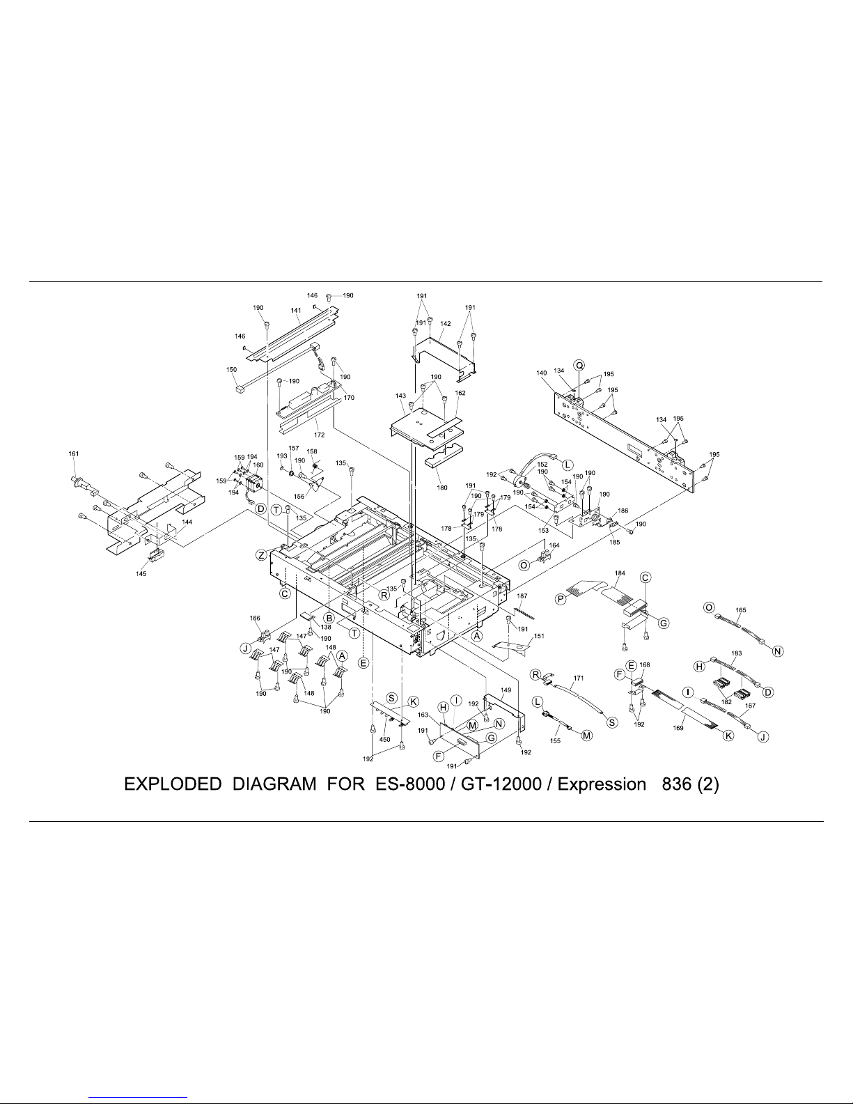
GT-12000 Appendix
Rev. A
7-11
Figure 7-7. Exploded Diagrams (2)
Page 71

SERVICE MANUAL
ADF (Auto Document Feeder)
4008512
®
Page 72

NOTICE
n All rights reserved. No part of this manual may be reproduced, stored in a retrieval system, or transmitted in any form or by any means, electronic,
mechanical, photocopying, recording, or otherwise, without the prior written permission of SEIKO EPSON CORPORATION.
n The contents of this manual are subject to change without notice.
n All effort have been made to ensure the accuracy of the contents of this manual. However, should any errors be detected, SEIKO EPSON would greatly
appreciate being informed of them.
n The above not withstanding SEIKO EPSON CORPORATION can assume no responsibility for any errors in this manual or the consequences thereof.
EPSON is a registered trademark of SEIKO EPSON CORPORATION.
General Notice: Other product names used herein are for identification purpose only and may be trademarks or registered trademarks of their respective
owners. EPSON disclaims any and all rights in those marks.
Copyright © 1996 SEIKO EPSON CORPORATION. Printed in Japan.
Page 73

PRECAUTIONS
Precautionary notations throughout the text are categorized relative to 1)Personal injury and 2) damage to equipment.
DANGER
Signals a precaution which, if ignored, could result in serious or fatal personal injury. Great caution should be exercised in performing
procedures preceded by DANGER Headings.
WARNING
Signals a precaution which, if ignored, could result in damage to equipment.
The precautionary measures itemized below should always be observed when performing repair/maintenance procedures.
DANGER
1. ALWAYS DISCONNECT THE PRODUCT FROM THE POWER SOURCE AND PERIPHERAL DEVICES PERFORMING ANY MAINTENANCE OR
REPAIR PROCEDURES.
2. NOWORK SHOULD BE PERFORMED ON THE UNIT BY PERSONS UNFAMILIER WITH BASIC SAFETY MEASURES AS DICTATED FOR ALL
ELECTRONICS TECHNICIANS IN THEIR LINE OF WORK.
3. WHEN PERFORMING TESTING AS DICTATED WITHIN THIS MANUAL, DO NOT CONNECT THE UNIT TO A POWER SOURCE UNTIL
INSTRUCTED TO DO SO. W HEN THE POWER SUPPLY CABLE MUST BE CONNECTED, USE EXTREME CAUTION I N WORKING ON POWER
SUPPLY AND OTHER ELECTRONIC COMPONENTS.
WARNING
1. REPAIRS ON EPSON PRODUCT SHOULD BE PERFORMED ONLY BY AN EPSON CERTIFIED REPAIR TECHNICIAN.
2. MAKE CERTAIN THAT T HE SOURCE VOLTAGES IS THE SAME AS THE RAT ED VOLTAGE, LISTED ON T HE SERIAL NUMBER/RATING PLATE. I F
THE EPSON PRODUCT HAS A PRIMARY AC RATING DIFFERENT FROM AVAILABLE POW ER SOURCE, DO NOT CONNECT IT T O THE POW ER
SOURCE.
3. ALWAYS VERIFY THAT T HE EPSON PRO DUCT HAS BEEN DISCO NNECT ED FROM THE PO WER SOURCE BEFORE REMOVING OR REPLACI NG
PRINTED CIRCUIT BOARDS AND/OR INDIVIDUAL CHIPS.
4. I N ORDER TO PROTECT SENSITIVE MICROPROCESSORS AND CIRCUI TRY, USE STATIC DISCHARGE EQUI PMENT, SUCH AS ANTI-STATIC
WRIST STRAPS, WHEN ACCESSING INTERNAL COMPONENTS.
5. REPLACE MALFUNCTIONING COMPONENTS ONLY WITH THOSE COMPONENTS BY THE MANUFACTURE; INTRODUCTION OF SECONDSOURCE ICs OR OTHER NONAPPROVED COMPONENTS MAY DAMAGE THE PRODUCT AND VOID ANY APPLICABLE EPSON WARRANTY.
Page 74

PREFACE
This manual describes basic functions, theory of electr ical and mechanical operations, maintenance and repair procedures of ADF. The instructions and
procedures included herein are intended for the experienced repair technicians, and attention should be g iven to the precaution s on the preceding page. T he
chapters are organized as follows:
CHAPTER 1. PRODUCT DESCRIPTIONS
Provides a general overview and specifications of the product.
CHAPTER 2. OPERATING PRINCIPLES
Describes the theory of electrical and mechanical operations of the product.
CHAPTER 3. TROUBLESHOOTING
Provides the step-by-step procedures for troubleshooting.
CHAPTER 4. DISASSEMBLY AND ASSEMBLY
Describes the step-by-step procedures for disassembling and assembling the
product.
CHAPTER 5. ADJUSTMENTS
Provides Epson-approved methods for adjustment.
CHAPTER 6. MAINTENANCE
Provides preventive maintenance procedures and the lists of Epson-approved
lubricants and adhesives required for servicing the product.
APPENDIX
Provides the following additional information for reference:
• Connector pin assignments
• Electric circuit boards components layout
• Exploded diagram
• Electrical circuit boards schematics
Page 75

REVISION STATUS
Rev. Date Page(s) Contents
A 1997/10/20 All First release
Page 76

TABLE OF CONTENTS
PRODUCT DESCRIPTIONS
1.1 FEATURES....................................................................................................................................................................1-1
1.2 PRODUCT DESCRIPTION............................................................................................................................................1-1
OPERATING PRINCIPLES
2.1 OVERVIEW....................................................................................................................................................................2-1
2.1.1 ADF Mechanism..................................................................................................................................................................................2-1
2.1.2 Electrical Circuit ...............................................................................................................................................................................2-12
2.1.2.1 Transmission Circuit................................................................................................................................................................2-12
2.1.2.2 Paper Size Detection Circuit ...................................................................................................................................................2-13
2.1.2.3 Document Sensor (Empty Sensor) Circuit...............................................................................................................................2-13
2.1.2.4 Paper Feeding Motor Encoder Sensor Circuit.........................................................................................................................2-14
2.1.2.5 Registration Sensor Circuit......................................................................................................................................................2-14
2.1.2.6 Sensor Circuits........................................................................................................................................................................2-15
2.1.2.7 Switch Circuits.........................................................................................................................................................................2-16
2.1.2.8 Reset Circuit............................................................................................................................................................................2-16
2.1.2.9 Paper Feed Motor Driver Circuit..............................................................................................................................................2-17
2.1.2.10 Transportation/Paper Eject/Reverse Motor Driver Circuits.............................................................................................2-18
2.1.2.11 Feeding Solenoid/Reverse Solenoid Sensor Circuits ............................................................................................................2-19
2.1.2.12 Rush Current Limitation Circuit .............................................................................................................................................2-19
2.1.2.13 EEPROM Transmission/Write Circuit....................................................................................................................................2-20
Page 77

TROUBLESHOOTING
3.1 OVERVIEW....................................................................................................................................................................3-1
3.1.1 Test Mode Overview...........................................................................................................................................................................3-1
3.1.1.1 Single Feeding Test Mode ........................................................................................................................................................3-2
3.1.1.2 Reverse Feeding Test Mode.....................................................................................................................................................3-2
3.1.1.3 Single Feeding Without Paper Aging Test Mode ......................................................................................................................3-3
3.1.1.4 Reverse Feeding Without Paper Aging Test Mode...................................................................................................................3-3
3.1.1.5 Motor Line Output Test Mode....................................................................................................................................................3-4
3.1.1.6 Solenoid Line Output Test Mode...............................................................................................................................................3-4
3.1.2 Motor/Solenoid Internal Coil Resistance..........................................................................................................................................3-5
3.1.2.1 Transportation Motor Check Points...........................................................................................................................................3-5
3.1.2.2 Paper Eject/Reverse Motor Check Point...................................................................................................................................3-6
3.1.2.3 Solenoid Check Point................................................................................................................................................................3-6
3.1.2.4 Paper Size Sensor ....................................................................................................................................................................3-6
DISASSEMBLY AND ASSEMBLY
4.1 OVERVIEW....................................................................................................................................................................4-1
4.1.1 Tools....................................................................................................................................................................................................4-1
4.1.2 Screws................................................................................................................... ..............................................................................4-1
4.2 DISASSEMBLY PROCEDURE......................................................................................................................................4-2
4.2.1 Paper Feed Tray Removal..................................................................................................................................................................4-2
4.2.2 Control Board Unit Removal..............................................................................................................................................................4-3
4.2.3 Transportation Belt Unit Removal.....................................................................................................................................................4-4
4.2.4 Paper Feed Unit Removal...................................................................................................................................................................4-5
4.2.5 Paper Eject/Reverse Unit Removal ...................................................................................................................................................4-6
4.2.6 Transportation Belt Drive Motor Removal........................................................................................................................................4-7
Page 78

4.2.7 Paper Feed Motor Unit Removal........................................................................................................................................................4-8
4.2.8 Registration/Timing Sensor Removal...............................................................................................................................................4-9
4.2.9 Paper Eject/Reverse Motor Unit Removal.......................................................................................................................................4-10
4.2.10 Paper Eject Sensor Removal.........................................................................................................................................................4-11
ADJUSTMENT
5.1 OVERVIEW....................................................................................................................................................................5-1
5.1.1 Adjustment Tools................................................................................................................................................................................5-1
5.1.2 Mechanical Adjustment......................................................................................................................................................................5-1
5.1.2.1 Flapper Solenoid Installation Position Adjustment....................................................................................................................5-2
5.1.2.2 Separation Plate Gap Adjustment.............................................................................................................................................5-3
5.1.2.3 Belt Tension Adjustment...........................................................................................................................................................5-4
5.1.2.4 Magnet Catch Installation Position Adjustment.........................................................................................................................5-4
5.1.2.5 Micro Switch Installation Position Adjustment...........................................................................................................................5-5
5.1.2.6 Skew Correction Adjustment.....................................................................................................................................................5-6
5.1.3 Electrical Adjustment.........................................................................................................................................................................5-7
5.1.3.1 Sensor Adjustment....................................................................................................................................................................5-8
5.1.3.2 EEPROM Initialize and Sensor Adjustment ..............................................................................................................................5-9
5.1.3.3 Scan Stop Position Adjustment.................................................................................................................................................5-9
Page 79

MAINTENANCE
6.1 OVERVIEW....................................................................................................................................................................6-1
6.1.1 Cleaning...............................................................................................................................................................................................6-1
6.1.1.1 Cleaning Points.........................................................................................................................................................................6-2
6.1.2 Lubrication..........................................................................................................................................................................................6-7
6.1.3 Adhesion ...........................................................................................................................................................................................6-15
APPENDIX
7.1 CONNECTOR TABLE ...................................................................................................................................................7-1
7.2 EXPLODED DIAGRAMS...............................................................................................................................................7-3
Page 80

PRODUCT DESCRIPTIONS
CHAPTER
1
Page 81

ADF Product Description
Rev. A
1-1
1.1 FEATURES
This auto document feeder (ADF) is the exclusive ADF for GT-12000, and
its main features are as follows:
q Supports large document up to A3 size
q Page transportation system
Document is transported page by page for each scanning operation
q Supports duplex feeding function
- Document is automatically reversed for scanning.
1.2 PRODUCT DESCRIPTION
BASIC SPECIFICATION
Type: Page transportation & duplex scanning type
Document transportation: - Document center aligning
- Fed faced-up from the bottom
- Face-up ejection
Document replacement time:1.2 seconds (A4/LT landscape)
Loading plural sizes: Unavailable (Size of the document in a stack
must be the same.)
Noise: 50dB or less
Page 82

ADF Product Description
Rev. A
1-
2
Accuracy in top position: Single feed: 0 - +2 mm
Duplex feed: 0 - +2 mm
Center alignment: Single feed: +1.5 mm
Duplex feed: +3 mm
Document skew: Single feed: +1.5 mm
Duplex feed: +3 mm
* Center alignment = (C+D)/2
* Skew amount = (A-B)x200/L
A
B
C
D
L
D ocum ent
D ocum ent G lass
Figure 1-1. Paper Feed Accuracy
DOCUMENT SUPPORTED
Document size: [Portrait] A3, LD, B4, LG, A4, LT, B5, A5,
140X148 mm / 5.5 x 5.8 inch
[Landscape] A4, LT, B5, A5
Feeding capacity: 50 sheets (80 g/m
2
)
- A4 landscape/portrait
- LT landscape/portrait or smaller
30 sheets (80 g/m
2
)
- B4, LG or larger
Ejecting capacity: 100 sheets
Applicable document [Paper Type]
- High quality paper
- Average quality paper
- Ink-jet paper (fine/super fine equivalent)
- Bond paper
[Paper thickness] 50 - 127 g/m
2
Document whose thickness is more than
110g/m
2
is applicable in the normal
condition* only.
(Normal condition : 15 - 25° C, 40 - 70%).
Inapplicable document: - Tracing paper, Coating paper, Pasted
paper, Label paper, OHP film, Carbon
paper, Catalogue paper,
Special paper including rice paper
- Stapled paper, Clipped paper
- Paper with many holes
(ex, loose-leaf paper)
- Paper with rip, curl and bent
Page 83

ADF Product Description
Rev. A
1-
3
ELECTRICAL SPECIFICATION
Power supply: Supplied through the scanner
- DC24V ± 10%
- DC5V ± 10%
Consumption current: DC24V = 2.0A
DC5V = 0.3A
Insulation resistance: 10 mW or more at DC500V
(Between AC line and chassis)
Dielectric strength: AC1000V per minute
(Between AC line and chassis)
Resistance to static electric
noise: Case = Operated properly at 10KV or less
Metal =Operated properly at 7KV or less
ENVIRONMENTAL CONDITION
Temperature: - Operation = 5 - 35°C
- Storage = -25 - 60°C
Humidity: - Operation = 10 - 80% *
- Storage = 10 - 85% *
* Without condensation
Resistance to vibration: - Operation = 0.2G / 5 - 55Hz
in X,Y,Z directions
- Storage = 2G / 5 - 55Hz
in X,Y,Z directions
Dropping test: Height = 62 cm / 24.2 inch*
* When packed.
RELIABILITY
Paper feeding life: 100,000 sheets
Paper ejecting life: 100,000 sheets
Hinge: 100,00 close motions or more
SAFETY, EMC
Safety regulations: - UL1950
- CSA950
- FCC
CE Marking: - Directive 89/336EEC, 92/31 EEC
- Directive 73/23 EEC
OPERATING CONDITION
Environment: Ordinal office or home conditions.
(Place with extreme dust should be avoided.)
Page 84

ADF Product Description
Rev. A
1-
4
APPEARANCE
Weight: 16Kg or less
Dimensions (W x D x H): 601 x 529 x 122 mm / 23.6 x 20.8 x 4.8 inch
(with the extension tray stored.)
601 m m / 23.6 inch
529 m m / 20.8 inch
122 m m
4.8 inch
147 m m
5.8 inch
Figure 1-2. External Dimensions of the ADF
Page 85

OPERATING PRINCIPLES
CHAPTER
2
Page 86

ADF Operating Principles
Rev. A
2-1
2.1 OVERVIEW
This chapter gives information on operating principles of the ADF which
can be used with the EPSON scanner GT-12000. The contents of this
chapter are as follows:
Section 2.1.1: ADF mechanism
q Single feeding
q Reverse feeding
Section 2.1.2: Electrical Circuit
q Sensor circuits
q Reset circuits
q Driver circuits
q Rush current limitation circuit
q EEPROM write circuit
2.1.1 ADF Mechanism
See Figure 2-1 which shows major mechanism parts of the ADF and their
locations. In both Single/Reverse feeding modes, docum ent is picked up
at the paper feed tray and is then transported in the ADF and eject ed to
the output tray. This process is described step by step t horough out the
section.
Descriptions for single and reverse feedings are given separately. As you
follows the steps, make sure that you refer to Figure 2-1 for exact
locations of the parts and their functions.
Em pty Sensor
Separation R oller
D ocum ent S hutter
D ocum ent W eight
H alf-m oon Roller
Paper Feed Tray
Paper Feed Roller
R egistration R oller
R egistration S ensor
Tim ing S ensor
D ocum ent W eight
Platen G lass
Transportation Belt
O u tp u t T ra y
Eject R oller
Flapper
Paper Eject/
Reverse Roller
Paper Eject/
R everse Sensor
Paper Feed M otor
(fo rw a rd )
W ait S hutter Solenoid
Paper Feed M otor
(backward)
Transportation M otor
(forw ard/backward)
Flapper Solenoid
Paper Eject/R everse M otor
(fo rw a rd on ly)
Figure 2-1. Major Mechanism Parts and Their Locations
Page 87

ADF Operating Principles
Rev. A
2-
2
SINGLE FEEDING
In single feeding mode, the ADF loads document from the paper feed t ray
and transports it to the scanning position, then ejects it immediately af ter
scanning. Therefore, document must be always transported in single
direction to let the ADF repeat feeding/ejecting operation cycle.
Setting document
1. Document is set in the paper feed tray.
Pre-feeding
"Pre-feeding" means the sequence in which the ADF transports document
from the paper feed tray to the scanning position according to the single
feed command sent from the scanner.
2. When the wait shutter solenoid turns on, the document is picked up
and transported from the paper feed tray by the forward rotation of
the paper feed motor. The motor then stops rotating when the
registration sensor comes on. This sequence, from picking up the
document to the registration sensor's coming on, is called registration
operation. The transportation motor and the paper eject/reverse
motor also rotate forward to perform dummy ejection to prevent a
remaining document from jamming when the ADF is feeding another
document. This is performed for every feeding motion no matter a
document is remaining in the ADF or not.
3. After the registration operation is carried out, the paper feed motor
starts rotating forward to transport the document. The document is
transported to the position where the timing sensor comes on, which
means the end of the pre-feeding operation. Ongoing dummy ejection
is carried out.
4. The transportation motor and paper feeding motor rotate forward and
backward, respectively, to transport the document onto the platen
glass. Then the document size is measured when the registration
sensor goes off and the paper feed motor stops rotating when the
timing sensor goes off.
Figure 2-2. Document Set Condition (Step 1)
Figure 2-3. Pre-feeding (Step 2)
Figure 2-4. Pre-feeding (Step 3)
Figure 2-5. Single Feeding (Step 4)
Page 88

ADF Operating Principles
Rev. A
2-
3
5. The document is transported until the rear edge passed the
document stopper, then the transportation motor stops rotating.
6. The transportation motor rotates backward to move the document
back until it bumps against the paper stopper, and the motor stops.
With the document aligned with the stopper, paper skew is corrected
and the document is ready to be scanned. The ADF sends the paper
feeding complete signal to the scanner.
7. While scanning is proceeding, the paper feed motor starts rotating
forward to pick up and transport the document. The motor stops when
the registration sensor comes on.
8. After the registration operation is carried out, the paper feed motor
rotates forward to transport the document to the position where the
timing sensor comes on, and the pre-feeding operation is done. Then
the ADF sends the operation complete signal to the scanner.
10 mm
Figure 2-6. Single Feeding (Step 5)
Im pact
Figure 2-7. Single Feeding (Step 6)
Figure 2-8. Single Feeding (Step 7)
Figure 2-9. Single Feeding (Step 8)
Page 89

ADF Operating Principles
Rev. A
2-
4
9. After scanned, the scanned document is ejected according to the
single feed command from the scanner and the pre-fed document is
transported to the scanning position.
10. After the document is fed by the forward rotation of the transportation
motor and the paper eject/reverse motor, the paper feed motor
rotates backward to transport the document onto the platen glass and
stops when the timing sensor goes off.
11. After the paper feed motor stops rotating, the transportation motor
transports the document and stops rotating when the rear edge of the
document passed the document stopper. In case the empty sensor
goes off while the document is transported, the shutter solenoid goes
off. The ADF continues to eject the scanned document.
12. Transportation motor rotates backward to feed back the fed
document to align it with the document stopper causing impact, then
the transportation motor stops. With the document set on the
scanning position, the ADF sends the paper feeding complete signal
to let the scanner start scanning. The ADF continues to eject the
scanned document.
Figure 2-10. Single Feeding (Step 9)
Figure 2-11. Single Feeding (Step 10)
Figure 2-12. Single Feeding (Step 11)
Figure 2-13. Single Feeding (Step 12)
Page 90

ADF Operating Principles
Rev. A
2-
5
13. While scanning, the document is ejected to the output tray. Rotational
speed of the paper eject/reverse motor is reduced when the paper
eject/reverse sensor is near off condition to output the document to
the output tray slowly.
14. The paper eject/reverse motor stops after outputting the document to
the tray slowly. The ADF sends the operation complete signal to the
scanner and waits for the next command to be sent.
15. When the ADF receives the ejection command, it starts ejecting the
scanned document. The transportation motor and the paper
eject/reverse motor rotate forward for this operation.
16. The paper eject/reverse motor reduces its rotational speed when the
paper eject/reverse sensor is near off condition to output the
document to the output tray slowly. The paper eject/reverse motor
then stops when the paper eject/reverse sensor goes off.
17. The ADF sends t he operation complete signal to the scanner when
the document is slowly ejected and the paper eject/reverse motor
stops rotating.
Figure 2-14. Single Feeding (Step 13)
Figure 2-15. Single Feeding (Step 14)
Figure 2-16. Single Feeding (Step 15)
Figure 2-17. Single Feeding (Step 16)
Figure 2-18. Single Feeding (Step 17)
Page 91

ADF Operating Principles
Rev. A
2-
6
REVERSE FEEDING
In the reverse feeding mode, document is fed in the following order:
The document is fed. ® The document is reversed. ®
Image is scanned ® The document is reversed again. ®
Image on the reversed side is scanned.
Setting a document
1. Document is set in the paper feeding tray.
Pre-feeding
"Pre-feeding" consists of operations which pick up the document from the
paper feed tray and transport it to the scanning position according to the
reverse feed command sent from the scanner.
2. Step 2) After the wait shutter solenoid turns on, the document is
picked up and transported from the paper feed tray by the forward
rotation of the paper feed motor. The motor then stops rotating when
the registration sensor comes on. This sequence, from picking up the
document to the registration sensor's coming on, is called registration
operation. The transportation motor and the paper eject/reverse
motor also rotate forward to perform dummy ejection to prevent a
remaining document from jamming when the ADF is feeding another
document. This is performed for every feeding motion no matter a
document is remaining in the ADF or not.
3. After the registration operation is carried out, the paper feed motor
starts rotating forward to transport the document. The document is
transported to the position where the timing sensor comes on, which
means the end of the pre-feeding operation. Ongoing dummy ejection
carries on.
4. The transportation motor and paper feed motor rotate forward and
backward, respectively, to transport the document onto the platen
glass. The paper feed motor stops rotating when the registration
sensor goes off. The flapper solenoid comes on to switch the paper
path to the paper eject/reverse mechanism side.
Figure 2-19. Setting a Document (Step 1)
Figure 2-20. Pre-feeding (Step 2)
Figure 2-21. Pre-feeding (Step 3)
Figure 2-22. Reverse Feeding (Step 4)
Page 92

ADF Operating Principles
Rev. A
2-
7
5. When the paper eject/reverse sensor comes on, the transportation
motor stops and then the paper eject/reverse motor stops to hold the
document in the paper eject/reverse mechanism.
6. The transportation motor rotates backward and then the paper
eject/reverse motor rotates forward to transport the document from
the paper eject/reverse mechanism to the scanning position on the
platen glass. The paper eject/reverse motor stops when the paper
eject/reverse sensor goes off. When the document bumps against the
paper stopper, transportation motor stops and the flapper solenoid
goes off to stop transporting the document. With the document set for
scanning, the ADF sends the paper feeding complete signal to the
scanner, and the scanner starts scanning.
7. The paper feed motor starts rotating forward to pick up and transport
another document from the paper feed tray. The motor stops when
the registration sensor comes on.
8. After the registration operation is carried out, the paper feed motor
rotates forward to transport the pre-fed document to the position
where the timing sensor comes on. The pre-feeding operation is
complete when the ADF sends the operation complete signal to the
scanner.
Figure 2-23. Reverse Feeding (Step 5)
Figure 2-24. Reverse Feeding (Step 6)
Figure 2-25. Reverse Feeding (Step 7)
Figure 2-26. Reverse Feeding (Step 8)
Page 93

ADF Operating Principles
Rev. A
2-
8
9. According to the reverse feeding command, the transportation motor
and the paper eject/reverse motor rotate forward to transport the
scanned document to the paper eject/reverse mechanism and the
flapper solenoid comes on to switch the paper path to the paper
eject/reverse mechanism side.
10. When the paper eject/reverse sensor comes on, the transportation
motor stops and then the paper eject/reverse motor stops to hold the
document in the paper eject/reverse mechanism.
11. The transportation motor rotates backward and then the paper
eject/reverse motor rotates forward to transport the document from
the paper eject/reverse mechanism to the scanning position on the
platen glass. The paper eject/reverse motor stops when the paper
eject/reverse sensor goes off. When the document bumps against the
paper stopper, transportation motor stops and the flapper solenoid
goes off to stop transporting the document. With the document set for
scan, the ADF sends the paper feeding complete signal to the
scanner, and the scanner starts scanning.
12. After scanning, the ADF starts ejecting the scanned document and
transporting the pre-fed document according to the reverse feeding
command. The transportation motor and the paper eject/reverse
motor rotate forward to transport the document to eject it.
Figure 2-27. Reverse Feeding (Step 9)
Figure 2-28. Reverse Feeding (Step 10)
Figure 2-29. Reverse Feeding (Step 11)
Figure 2-30. Reverse Feeding (Step 12)
Page 94
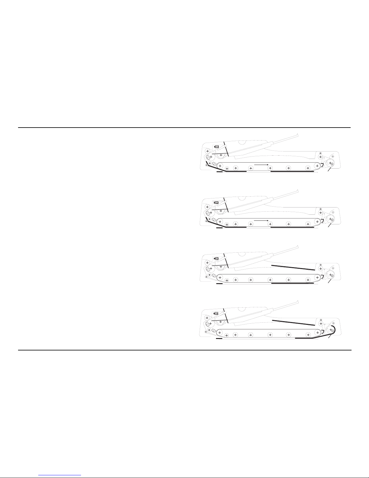
ADF Operating Principles
Rev. A
2-
9
13. The transportation motor rotates forward and then the paper feed
motor rotates backward to transport the pre-fed document to the
platen glass. The document size is measured when the registration
sensor goes off, and the paper feed motor stops when the timing
sensor goes off. The flapper solenoid also comes on to switch the
paper path to the paper eject/reverse mechanism side.
14. After the paper feed motor stops, the transportation motor starts
transporting the document and stops when the leading edge of the
document is near the paper eject/reverse mechanism to wait for the
scanned document to be ejected completely. In case the empty
sensor goes off while transporting, the shutter solenoid goes off.
15. After the scanned document is ejected, the flapper solenoid comes
on to switch the paper path to the paper eject/reverse mechanism
side. The transportation motor and the paper eject/reverse motor
rotate forward to transport the fed document to the paper
eject/reverse mechanism.
16. When the paper eject/reverse sensor comes on, the transportation
motor stops. Then the paper eject/reverse motor stops to hold the
document in the paper eject/reverse mechanism.
Figure 2-31. Reverse Feeding (Step 13)
Figure 2-32. Reverse Feeding (Step 14)
Figure 2-33. Reverse Feeding (Step 15)
Figure 2-34. Reverse Feeding (Step 16)
Page 95

ADF Operating Principles
Rev. A
2-1
0
17. The transportation motor rotates backward and then the paper
eject/reverse motor rotates forward to transport the document from
the paper eject/reverse mechanism to the scanning position. The
paper eject/reverse motor stops when the paper eject/reverse sensor
goes off and the transportation motor stops when the document
bumps against the paper stopper. Document transportation stops
when the flapper solenoid goes off. With the document set for scan,
the ADF sends the paper feeding complete signal to the scanner, and
the scanner starts scanning.
18. After scanning, the ADF starts transporting the scanned document
back to the scanning position via the paper eject/reverse mechanism.
The transportation motor and the paper eject/reverse motor rotate
forward to transport the scanned document to the paper eject/reverse
mechanism and the flapper solenoid comes on to switch the paper
path to the paper eject/reverse mechanism side.
19. When the paper eject/reverse sensor comes on, the transportation
motor stops and then the paper eject/reverse motor stops to hold the
document in the paper eject/reverse mechanism.
20. The transportation motor rotates backward and then the paper
eject/reverse motor rotates forward to transport the document from
the paper eject/reverse mechanism to the scanning position. The
paper eject/reverse motor stops when the paper eject/reverse sensor
goes off and the transportation motor stops when the document
bumps against the paper stopper. With the document set for scan,
the ADF sends the paper feeding complete signal to the scanner, and
the scanner starts scanning.
Figure 2-35. Reverse Feeding (Step 17)
Figure 2-36. Reverse Feeding (Step 18)
Figure 2-37. Reverse Feeding (Step 19)
Figure 2-38. Reverse Feeding (Step 20)
Page 96

ADF Operating Principles
Rev. A
2-11
21. According to the ejection command from the scanner, the scanner
starts ejecting the scanned document. The transportation motor and
the paper eject/reverse motor rotate forward to eject the scanned
document.
22. When the paper eject/reverse sensor is near off condition, rotational
speed of the paper eject/reverse motor is reduced to eject the
document slowly to the output tray. The transportation motor stops
when the paper eject/reverse sensor goes off.
23. The paper eject/reverse motor stops after the document is ejected to
the output tray and the ADF sends the operation complete signal to
the scanner.
Figure 2-39. Reverse Feeding (Step 21)
Figure 2-40. Reverse Feeding (Step 22)
Figure 2-41. Reverse Feeding (Step 23)
Page 97

ADF Operating Principles
Rev. A
2-1
2
2.1.2 Electrical Circuit
This ADF (R-4C1070).is equipped with only one control board. This
section describes the functions of the board.
2.1.2.1 Transmission Circuit
The transmission circuit manages parallel and serial signal transmission
between the ADF and the scanner. The protocol used between them is
original.
q Serial transmission
IC11 is the transceiver used for the serial transmission. It receives
output signal from the CPU and separates them according to the
signal types; reversed or non-reversed, then it outputs the signals to
the scanner from DO1. 2 signals (RI1 and RI2) sent from the scanner
are combined into 1 signal and output from the RO1.
q Parallel transmission
Signals sent from the CPU is output at the open collector via IC1 and
IC3. Signals from the scanner are transferred to the CPU via the pullup resistor.
TXD
1
2
3
4
5
6
7
8
9
*TXD
RXD
*RXD
DTR
DSR
GND
OP1
OP2
GND
DTR
B
A
Y
IC1
Q3
+5V
R36
1.0K
DSR
R64
4.7K
CN6
R81
220
DA2
+5V
GND
DA1
GND
IC11
GND
R35
1K
79
80
21
3
4
15
5
9
1
2
14
13
6
7
10
11
CPU
GND
*RI1
RI1
DO1
*DO1
*RI2
RI2
DO2
*DO2
RO1
DI1
*RE
DE
RO2
DI2
RXD
TXD
TXEN
R63
4.7K
R62
4.7K
IC12
Figure 2-42. Transmission Circuit Block Diagram
Page 98

ADF Operating Principles
Rev. A
2-1
3
2.1.2.2 Paper Size Detection Circuit
The edge guides in the paper feed tray of this ADF are used to detect the
paper size. As they move, slide resistance changes in accordance with the
distance between them. The resistance is then converted into analog data
and transferred to the CPU, where the paper size is determined. This
circuit consists of the RC noise filter.
1
2
3
+5V
DWVR
GND
+5V
10K
R11
GND
C41
0.01 uF
GND
TP24
AN17
63
IC12
CPU
C62
0.01 uF
CN1
Figure 2-43. Document Width Detection Circuit Block Diagram
2.1.2.3 Document Sensor (Empty Sensor) Circuit
A photo-interrupter sensor located at the bottom of the paper feed tray is
used to detect document. The ADF determines whether or not it continues
pre-feeding based on the signal sent from this sensor. The signal is
transferred to the CPU via the resistors only.
1
2
3
CN1
EMP
SGND
+5V
TP16
P67
20
IC12
CPU
GND
+5V
180
15
10K
Figure 2-44. Document Sensor Circuit Block Diagram
Page 99

ADF Operating Principles
Rev. A
2-1
4
2.1.2.4 Paper Feeding Motor Encoder Sensor Circuit
The paper feeding motor is used to manage the following operations:
q Registration operation
q Drives the transportation motor after the timing sensor goes off.
q Controlling backward rotation of the motor
Since this motor is used for various operations, the mot or rot ation must be
precisely controlled. Failure in controlling the motor does not guarantee
prompt feeding, or may result in jamming caused by the document
inserted over the document remaining in the ADF. The m otor rotation is
controlled according to the signal form the photo-int errupter which detects
the slid plate directly attached to the motor shaft. The signal is output to
the CPU via the resistors only.
1
2
3
+5V
KM CLK
GND
+5V
TP20
INTP2
74
IC12
CPU
GND
CN1
R82
180
R61
10K
R14
10K
Figure 2-45.
Paper Feeding Motor Encoder Sensor Circuit Block Diagram
2.1.2.5 Registration Sensor Circuit
The registration sensor with an LED and the photo tr ansistor built in has
an mirror attached across the paper path. Since t he registration sensor is
a reflex type sensor, it detects paper empty condit ion by emitting infr ared
light from the LED toward the mir ror and receiving the light reflected on
the mirror.
The voltage input to the sensor is divided by R55 and R56, and 1/3 of the
original level is input to the AD converter of the CPU. (Actually, it is
regulated to 5 V by D2.) Analog data fo r the input voltage is output one
after another in a rectangle waveform from IC4 via PWM circuit in the gate
array. This PWM signal is integ rated via R3 and C6 of the C,R circuit and
converted into the analog voltage. Then it is am plified by the non-reverse
amplifier to establish the reference value for the comparator. Therefore,
the reference value is set to 1/3 of the High level of each sensor output
timing. In case the voltage level input to the AD converter of the CPU
drops below 1.6 V, the CPU outputs High from Pin 48 to increase LED
emission.
13
14
15
AN+24V
REGS
RDDLED
CN1
IC4-18
RDDPWM
R3
10K
AGND
C44
0.01uF
R38
22 K
IC5
+
C6
0.01uF
AGND
R39
22K
R60
4.7K
C40
0.01uF
AGND
IC6
+
R56
100K
R23
10K
+5V
+5V
AN+24V
TP19
73
TP14
R68
2.7 K
R69
5.6 K
AGND
10K
R65
10K
TP23
D2
R4
10K
56
C16
0.1uF
R55
4.7K
AGND
Q4
48
IC12
CPU
INTP1
ANIO
P11
Figure 2-46. Registration Sensor Circuit Block Diagram
Page 100

ADF Operating Principles
Rev. A
2-1
5
2.1.2.6 Sensor Circuits
The timing sensor and the paper eject/reverse sensor are reflex type
sensors, and each of them has an LED and photo-transistor built in it.
Each sensor emits infrared light from the LED toward the mirror attached
across from the sensor and detects paper empty condition when it
receives the infrared light reflected on the mirror.
The cathode of the LED is connected to the collector of Q3. Current output
to the photo diode is controlled at the terminal AN0 of the CPU.
Photoelectric current from the photo transistor is converted into voltage via
the resistor in the input circuit of the sensor, and is input to the
comparator, where the voltage level is compared with the reference
voltage (2V).
If the input voltage is higher than the reference voltage, it means the
paper empty condition, and the compactor outputs a Low signal to the
CPU. Since sensors are generally produced with uneven sensitivities, the
CPU adjusts the input voltage from t he sensor to the specified level. When
the ADF is turned on under the paper empty condition, the input voltage
(analog data) from the sensor is input to the CPU as a digital data. The
CPU then manipulates the data to make the proper level of output voltag e
(analog data). After this process, the cur rent flows to the LED changes
and the input voltage from the sensor is adjusted to the proper level as the
result.
10
12
+5V
TIMS DA
CN1
+5V
TP13
-
+
IC12
CPU
ANO0
INTP0
ANI1
C49
1000uF
GND
R73
100
R17
100
IC5
Q13
67
+5V
TP11
R25
10K
-
+
+5V
R46
22K
R77
15K
AGND
R58
200K
IC6
72
57
AGND
C38
0.1uF
AGND
R18
10K
R67
3K
11
TIMS
CN1
Figure 2-47.
Timing Sensor Circuit / Reverse Sensor Circuit Block Diagrams
 Loading...