

Page 1

EP-3VEP-3V
EP-3V
EP-3VEP-3V
CA2CA2
CA2
CA2CA2
A SocA Soc
A Soc
A SocA Soc
mainboard (133/100/66MHz)mainboard (133/100/66MHz)
mainboard (133/100/66MHz)
mainboard (133/100/66MHz)mainboard (133/100/66MHz)
SupporSuppor
Suppor
SupporSuppor
TRADEMARK
All products and company names are trademarks or registered
trademarks of their respective holders.
These specifications are subject to change without notice.
kk
et 370 Pret 370 Pr
k
et 370 Pr
kk
et 370 Pret 370 Pr
ts PC-133 SDRAM Modulets PC-133 SDRAM Module
ts PC-133 SDRAM Module
ts PC-133 SDRAM Modulets PC-133 SDRAM Module
ocessor based 4X ocessor based 4X
ocessor based 4X
ocessor based 4X ocessor based 4X
Manual Revision 1.1
June 29, 2000
AA
A
AA
GPGP
GP
GPGP
Page 2

EP-3VCA2
User Notice
No part of this product, including the product and software may be reproduced,
transmitted, transcribed, stored in a retrieval system, or translated into any language
in any form without the express written permission of EPoX Computer Company
(hereinafter referred to as EPoX) except for documentation kept by the purchaser
for backup purposes.
We provide this manual as is without warranty of any kind, either expressed or
implied, including but not limited to the implied warranties or conditions of
merchantability or fitness for a particular purpose. In no event shall EPoX be liable
for any loss of profits, loss of business, loss of use or data, interruption of business or for indirect, special incidental, or consequential damages of any kind, even
if EPoX has been advised of the possibility of such damages arising from any
defect or error in the manual or product. EPoX may revise this manual from time
to time without notice. For updated BIOS, drivers, or product release information
you may visit our websites at http://www.epox.com or http://www.epox.com.tw.
Products mentioned in this manual are mentioned for identification purposes only.
Product names appearing in this manual may or may not be registered trademarks
or copyrights of their respective companies. The product name and revision
number are both printed on the mainboard itself.
Handling Procedures
Static electricity can severely damage your equipment. Handle the EP-3VCA2 and
any other device in your system with extreme care and avoid unnecessary contact
with system components on the mainboard. Always work on an antistatic surface to
avoid possible damage to the mainboard from static discharge. Always have the
power supply unplugged and powered off when inserting and removing devices
within the computer chassis. EPoX assumes no responsibility for any damage to
the EP-3VCA2 mainboard that results from failure to follow instruction or failure
to observe safety precautions.
CAUTION
The EP-3VCA2 mainboard is subject to
damage by static electricity. Always
observe the handling procedures.
Page 3

EP-3VCA2
Technical Support Services
If you need additional information, help during installation or normal use of this
product, please contact your retailer. Your retailer will have the most current
information about your configuration. If your retailer cannot help, you may visit
our online technical support website and/or contact our support technicians at the
locations listed below.
Record your serial number before installing your EP-3VCA2 mainboard. (The
serial number is located near the ISA slots at the edge of the board.)
EP-3VCA2 serial number: ____________________________
Contacting Technical Support
EPoX technical support is working hard to answer all of your questions online.
From our website you can find answers to many common questions, drivers, BIOS
updates, tech notes, and important technical bulletins. If you are still unable to
locate the solution you are seeking, you always have the option to contact our
support technicians directly.
North American website (English language)
http://www.epox.com
sales@epox.com
support@epox.com
European website (Multi-language)
http://www.epox.nl
sales@epox.nl
support@epox.nl
Taiwan website (Chinese language)
http://www.epox.com.tw
sales@epox.com.tw
support@epox.com.tw
Thank you for using EPoX mainboards!
Copyright 2000 EPoX Computer Company. All rights reserved.
Page 4

Section 1 Introduction
Components Checklist ........................................1-1
Overview
EP-3VCA2 Form-Factor ..................................... 1-2
I/O Shield Connector .......................................... 1-3
Power-On/Off (Remote)..................................... 1-3
System Block Diagram........................................ 1-4
Section 2 Features
EP-3VCA2 Features ............................................ 2-1
Section 3 Installation
EP-3VCA2 Detailed Layout ................................ 3-2
Easy Installation Procedure
CPU Insertion ...................................................... 3-3
Jumper Settings ................................................... 3-5
System Memory Configuration .......................... 3-7
Device Connectors ..............................................3-9
External Modem Ring-in Power ON and
Keyboard Power ON Function (KBPO) ............. 3-12
STR (Suspend To RAM) Function .......................3-13
EP-3VCA2
T able of Contents
Page
Section 4 Award BIOS Setup
BIOS Instructions ................................................ 4-1
Standard CMOS Setup ......................................... 4-2
BIOS Features Setup ........................................... 4-3
Chipset Features Setup ........................................ 4-8
Power Management Setup ................................... 4-11
PNP/PCI Configuration ...................................... 4-14
Load Setup Defaults ............................................ 4-16
Integrated Peripherals ......................................... 4-16
Sensor and CPU Speed Setup ..............................4-20
Change Supervisor or User Password................. 4-22
IDE HDD Auto Detection ...................................4-23
Page 5

EP-3VCA2
Appendix
Save & Exit Setup ................................................ 4-25
Exit Without Saving ............................................. 4-25
Appendix A
Memory Map ....................................................... A-1
I/O Map ................................................................ A-1
Timer & DMA Channels Map ............................. A-2
Interrupt Map ....................................................... A-2
RTC & CMOS RAM Map .................................... A-3
Appendix B
POST Codes......................................................... A-5
Unexpected Errors............................................... A-8
Appendix C
Load Setup Defaults ............................................ A-9
Appendix D
GHOST 5.1 Quick Users Guide ......................... A-11
Page 6

EP-3VCA2
Page Left Blank
Page 7
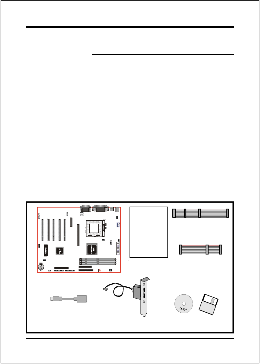
Components Checklist
üü
ü A. (1) EP-3VCA2 mainboard
üü
üü
ü B. (1) EP-3VCA2 users manual
üü
üü
ü C. (1) Floppy ribbon cable
üü
üü
ü D. (1) ATA-66 Hard drive ribbon cable
üü
E. (1) PS/2 to AT keyboard connector adapter (Optional)
F. (1) USB Cable (Optional)
üü
ü G. (1) Driver and utility
üü
IntroductionEP-3VCA2
Section 1
INTRODUCTION
USERS
MANUAL
EP-3VCA2
B
C
D
A
E
F
or
G
Page 1-1
Page 8
Introduction EP-3VCA2
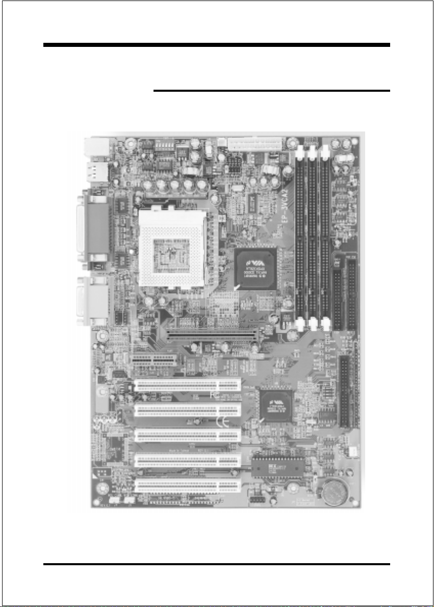
EP-3VCA2 F orm-Factor
The EP-3VCA2 is designed with ATX form factor - the new industry standard of
chassis. ATX form factor is essentially a Baby-AT baseboard rotated 90 degrees
within the chassis enclosure and a new mounting configuration for the power
supply. With these changes the processor is relocated away from the expansion
slots, allowing them all to hold full length add-in cards. ATX defines a double
height aperture to the rear of the chassis which can be used to host a wide range of
onboard I/O. Only the size and position of this aperture is defined, allowing PC
manufacturers to add new I/O features (e.g.; TV input, TV output, joystick, modem,
LAN, etc.) to systems. This will help systems integrators differentiate their
products in the marketplace, and better meet your needs.
By integrating more I/O down onto the board and better positioning the hard
drive and floppy connectors material cost of cables and add-in cards is
reduced.
By reducing the number of cables and components in the system, manufactur-
ing time and inventory holding costs are reduced and reliability will increase.
By using an optimized power supply, it's possible to reduce cooling costs and
lower acoustical noise. An ATX power supply, which has a side-mounted fan,
allows direct cooling of the processor and add-in cards making a secondary
fan or active heatsink unnecessary in most system applications.
Expandable I/O
Single chassis
fan for system
Full length
slots
Floppy / IDE
connectors
close to
peripheral
bays
Page 1-2
AT X
Power
Supply
3 1/2"
Bay
Figure 2: Summary of ATX chassis features
5 1/4"
Bay
CPU located near
Power Supply
ATX power connector
Page 9
IntroductionEP-3VCA2
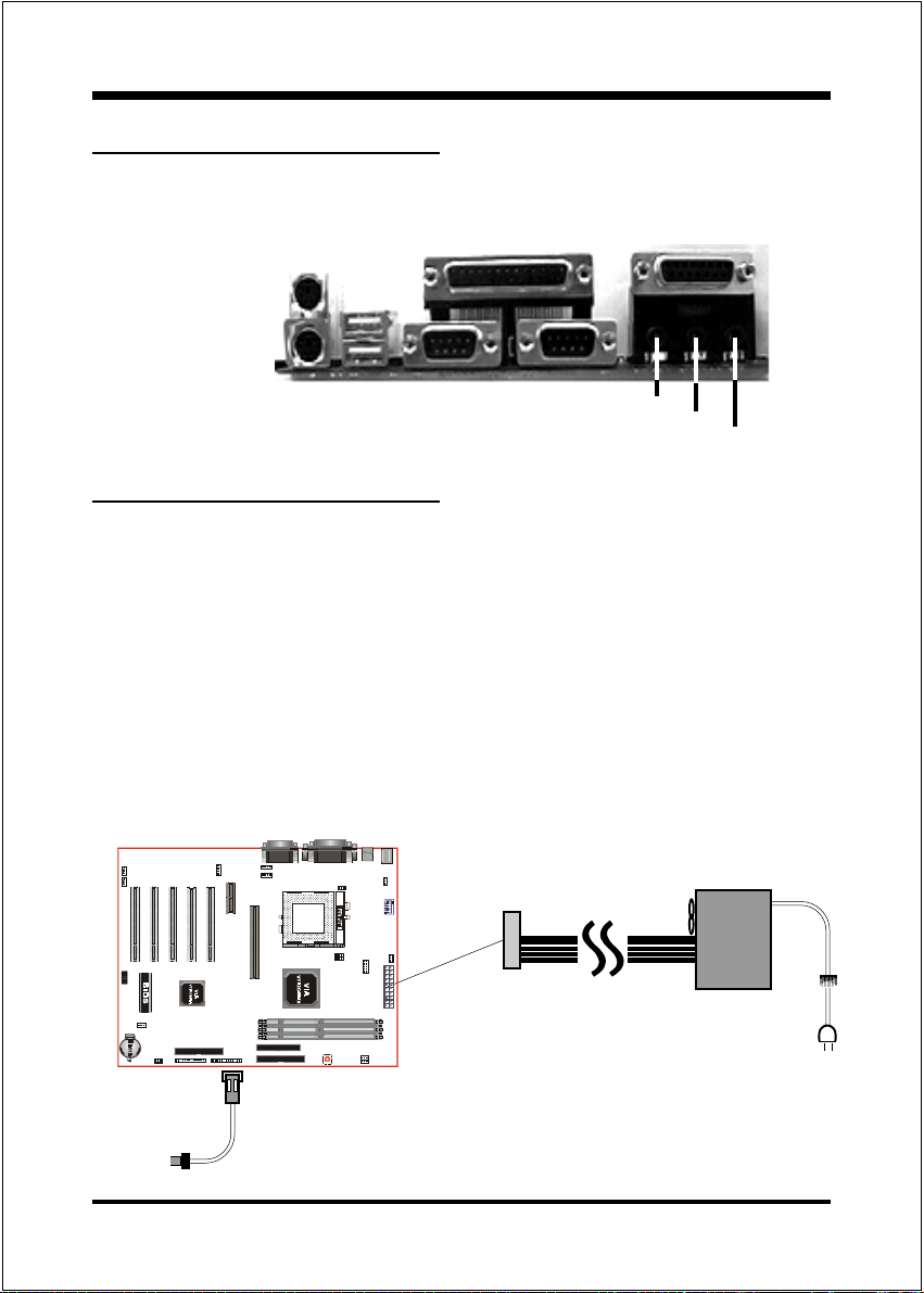
I/O Shield Connector
The EP-3VCA2 is equipped with an I/O back panel. Please use the appropriate I/
O shield (figure 3).
parallel port
Joystick/Midi
PS/2 Mouse
PS/2
KEYBOARD
USB port
COM1 COM2
Figure 3: I/O back panel layout
Speaker
Line_in
MIC
Power-On/Off (Remote)
The EP-3VCA2 has a single 20-pin connector for ATX power supplies. For ATX
power supplies that support the Remote On/Off feature, this should be connected
to the systems front panel for system Power On/Off button. The systems power
On/Off button should be a momentary button that is normally open.
The EP-3VCA2 has been designed with Soft Off" functions. You can turn Off the
system from one of two sources: The first is the front panel Power On/Off
button, and the other is the "Soft Off" function (coming from the EP-3VCA2s
onboard circuit controller) that can be controlled by the operating system such as
Windows 95/98. System will be turn off automatically after your click the START
button and resume the Shutdown selection.
ATX
POWER SUPPLY
J 3
Case (chassis) Power
ON/OFF button (J 3)
Figure 4: Simple ATX Power ON/OFF Controller
Page 1-3
Page 10
Introduction EP-3VCA2
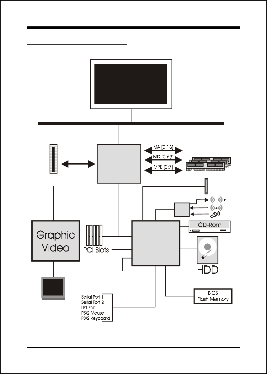
System Block Diagram
Socket 370
Proc essor
133/100/66MHz
AGP Slot
66MHz
AGP Bus
4X
PAC
PCI Bridge
and memory
controller
VT82C694X
VT82C686A
I/O Bridge
USB 0,1 USB 2,3
133/100/66MHz
AMR Slot
AC
97
Page 1-4
Figure 5: System Block Diagram
Page 11

FeaturesEP-3VCA2
Section 2
FEA TURES
EP-3VCA2 F eatures:
EP-3VCA2 is based on the Socket 370 Processors including PPGA & FC-
PGA operating at 300 ~ 800MHz.
Designed with VIA Apollo Pro 133A PCIset.
Supports up to 768MB of DRAM (minimum of 8 MB) on board (please
see Section 3-2).
EP-3VCA2 will support Error Checking and Correcting (ECC) when using
parity SDRAM memory modules. This will detect multiple bit errors and
correct 1-bit memory errors.
Supports (5) 32 bit PCI slots, (1) 4X AGP slot, (1) AMR slot and provides
(2) independent high performance PCI IDE interfaces capable of supporting
PIO Mode 3/4 and Ultra DMA 33/66 devices. The EP-3VCA2 supports (5)
PCI Bus Master slots and a jumperless PCI INT# control scheme which
reduces configuration confusion when plugging in PCI card(s).
Supports ATAPI (e.g. CD-ROM) devices on both Primary and Secondary
IDE interfaces.
Designed with on chip Multi I/O: (1) floppy port, (1) parallel port (EPP,
ECP), and (2) serial ports (16550 Fast UART).
Note: Japanese Floppy 3 mode is also supported
Features Award Plug & Play BIOS. With Flash Memory you can always
upgrade to the current BIOS as they are released. (http://www.epox.com/
please visit our Technical Support section for the latest updates).
EP-3VCA2 utilizes a Lithium battery which provides environmental
protection and longer battery life.
Page 2-1
Page 12

Features EP-3VCA2
4 USB ports are provided, 2 ports are onboard and another 2 USB ports, as
option, need USB an cable on USB2 position. The onboard VT82C686A chip
provides the means for connecting PC peripherals such as; keyboards,
joysticks, telephones, and modems.
Built-in ATX 20-pin power supply connector.
Software power-down when using Windows® 95/98.
Supports ring-in feature (remote power-on through external modem,
allows system to be turned on remotely).
Resume by Alarm - Allows your system to turn on at a preselected time.
Power Loss Recovery - In the event of a power outtage your system will
automatically turn itself back on without user intervention.
Supports CPU Hardware sleep and SMM (System Management Mode).
Supports Keyboard power ON function (KBPO).
Built-in WOL (Wake-up On Lan) Connector.
Built-in WOM (Wake-up On Modem) Connector.
Built-in AC97 PCI Audio.
Page 2-2
Page 13
InstallationEP-3VCA2
Section 3
INSTALLATION
Page 3-1
Page 14
Installation EP-3VCA2
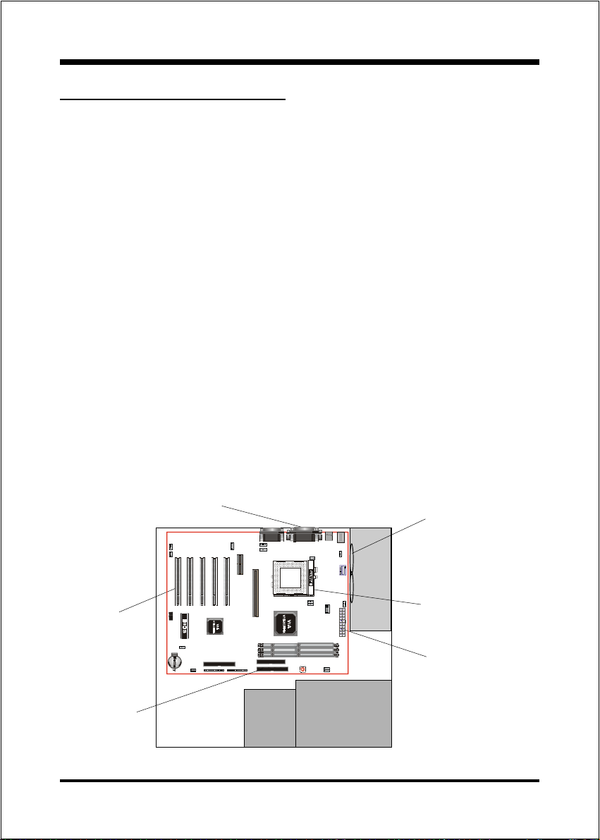
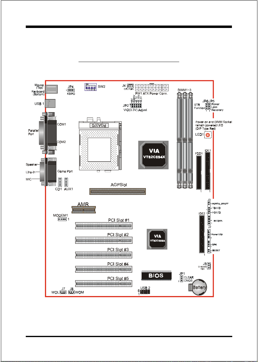
EP-3VCA2 Detailed Layout
Page 3-2
Figure 1
Page 15
InstallationEP-3VCA2
Easy Installation Procedure
The following must be completed before powering on your new system:
3-1. CPU Insertion
3-2. Jumper Settings
3-3. System memory Configuration
3-4. Device Connectors
3-5 External Modem Ring-in Power ON and Keyboard Power ON
Functions (KBPO)
3-6. STR Function
Section 3-1
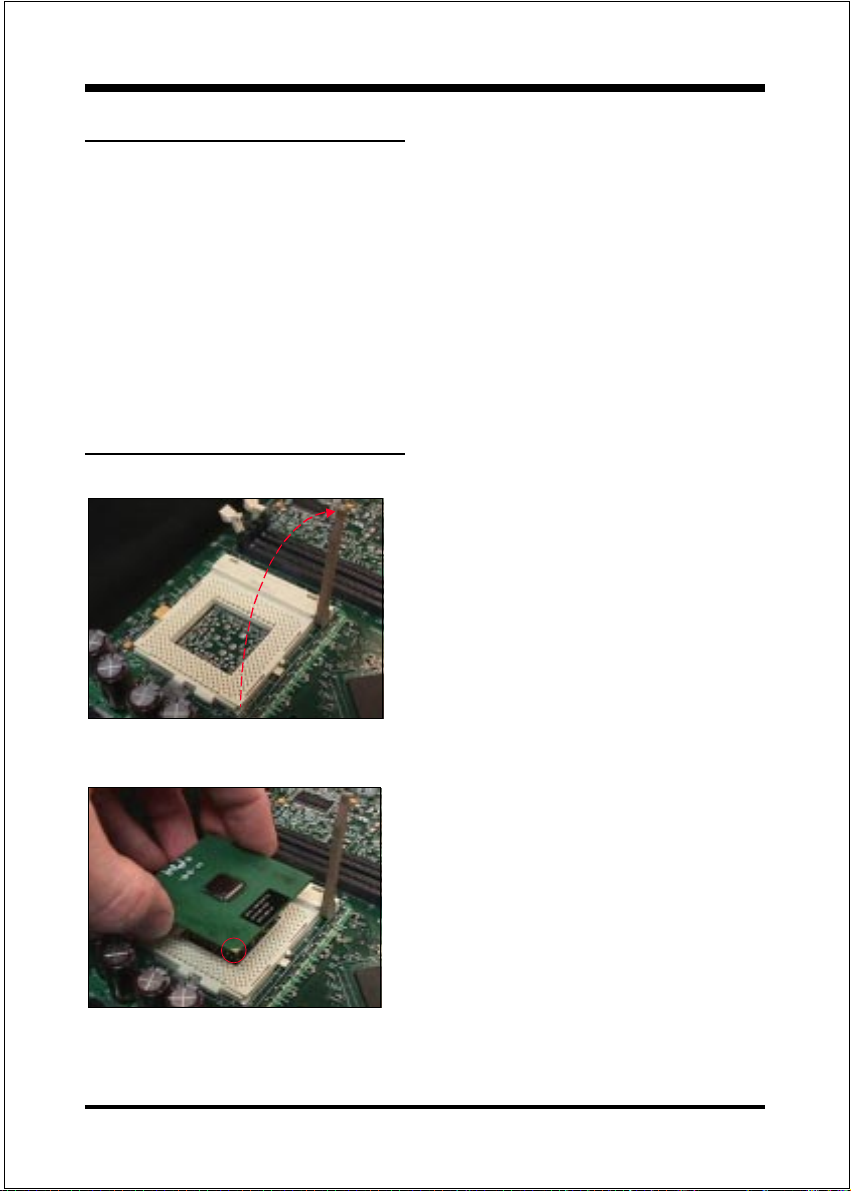
CPU Insertion
CPU Insertion: (use CuMineTM for reference)
Step 1
Open the socket by raising the actuation
lever.
Figure 2
Figure 3
Step 2
Insert the processor.
Ensure proper pin 1 orientation by aligning
the FC-PGA corner marking with the
socket corner closest to the actuation arm
tip. The pin field is keyed to prevent misoriented insertion.
Dont force processor into socket. If it does
not go in easily, check for mis-orientation and
debris.
Make sure the processor is fully inserted
into the socket on all sides.
Page 3-3
Page 16
Installation EP-3VCA2
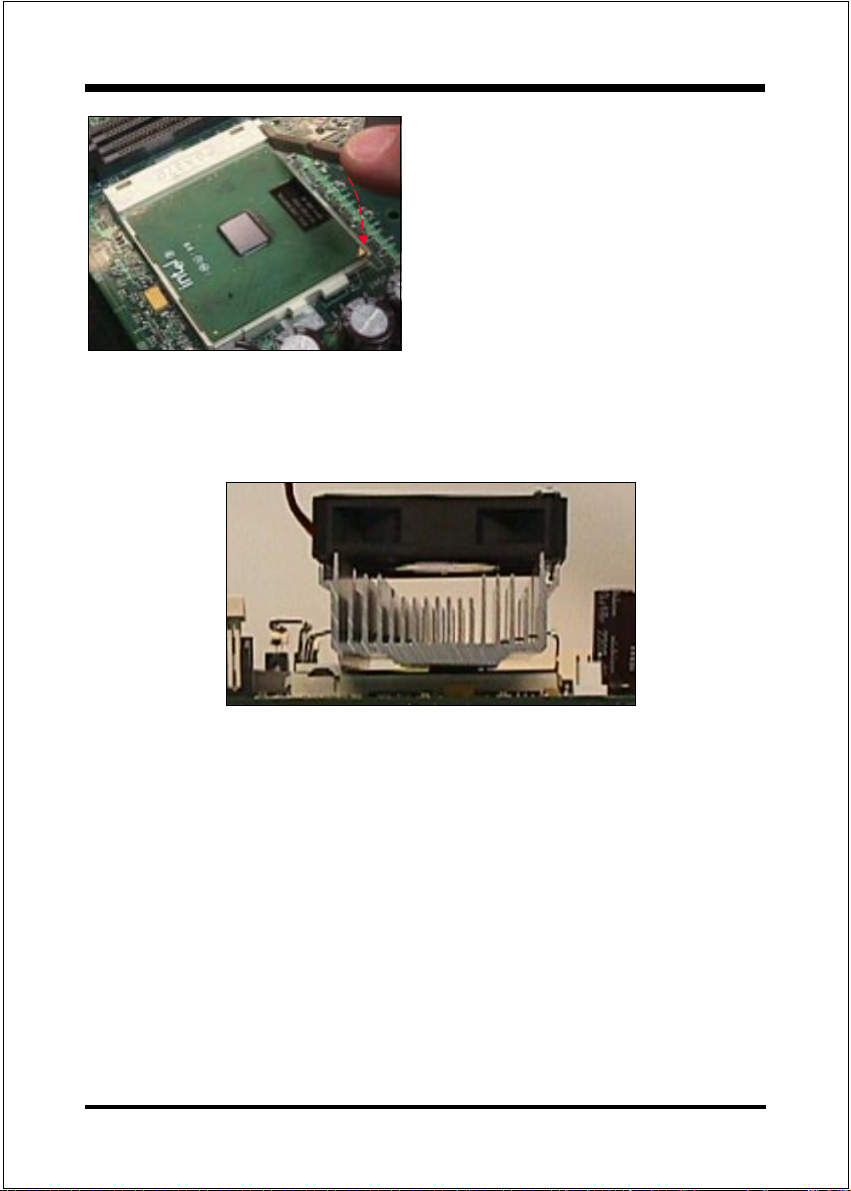
Step 3
Close the socket by lowering and
locking the actuation lever.
Figure 4
Note: Intels reference design thermal solution is an active heatsink; an extruded alumi-
num heatsink based and a fan attached to the top on the fin array. (See Figure 5)
Page 3-4
Figure 5
Page 17
InstallationEP-3VCA2
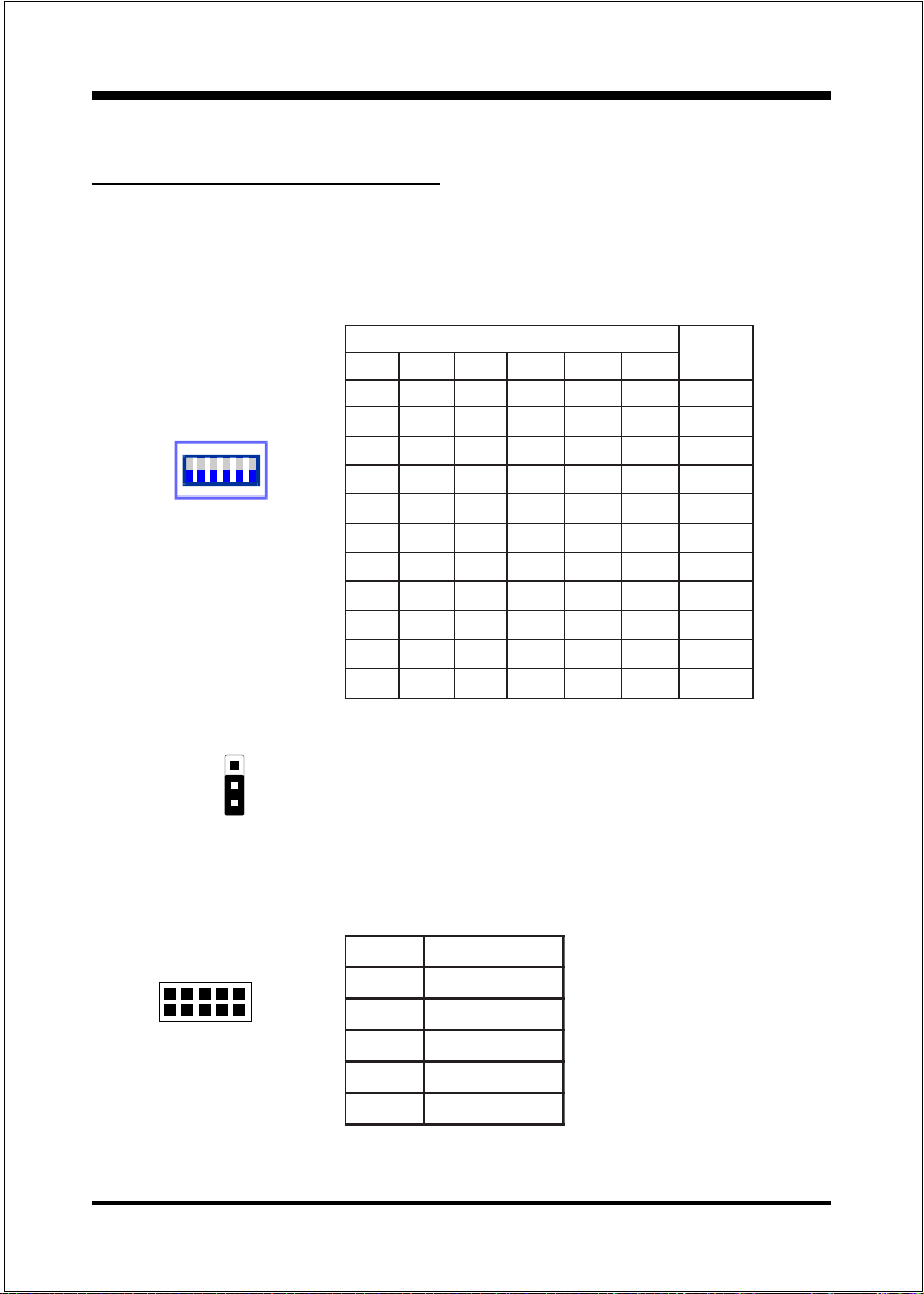
Section 3-2
Jumper Settings
The EP-3VCA2 motherboard was designed with very few jumpers to make your
installation faster and easier.
SW2: CPU Vcore Voltage Selection
123 4
NONONONO
ON
123456
NONONONONO
NONONONO
NONONONO
NONONONONO
NONONONONO
NONONONONONO
NONO
NONO
JP1 CMOS Clear
1
JP1 = 1-2 Normal (Default)
= 2-3 Clear CMOS
JP2: VIO (3.3V) Adjust Selection
2PJtsujdA)V3.3(OIV
6
10
15
6-1V0.0+
7-2V50.0+
8-3V1.0+
9-4V51.0+
01-5V2.0+
2WS
56
NONONO
UPC
erocV
OTUA
V6.1
V56.1
V7.1
V57.1
V8.1
V58.1
V0.2
V50.2
V1.2
V2.2
Page 3-5
Page 18

Installation EP-3VCA2
JP4 Keyboard Power-ON Function
1
JP4 = 1-2 Disabled (Default)
= 2-3 Enabled
JP5 Power Loss Recovery
1
JP5 = 1-2 Disabled
= 2-3 Enabled
JP6 STR Function
1
JP6 = 1-2 Disabled
= 2-3 Enabled
Page 3-6
Page 19

InstallationEP-3VCA2
Section 3-3
System Memory Configuration
Memory Layout
The EP-3VCA2 supports (3) PC133 168-pin DIMMs (Dual In-line Memory
Module). The DIMMs is for SDRAM (Synchronized DRAM).
DIMM SDRAM may be 83MHz (12ns), 100MHz (10ns) or
125MHz (8ns) bus speed.
If you use both 50ns and 60ns memory you must configure
your BIOS to read 60ns.
When using Synchronous DRAM we recommend using the
4 clock variety over the 2 clock.
Figure 6 and Table 1 show several possible memory configurations using both
SIMM and DIMM.
DIMM 1
DIMM 2
DIMM 3
Bank 0/1
Bank 2/3
Bank 4/5
-Synchronous
Figure 6
yromeMlatoT
BM652=
mumixaM
BM215=
mumixaM
BM867=
mumixaM
1MMID
)1/0knaB(
*MARDS
*MARDS
*MARDS
,BM46,BM23,BM61,BM8
1XBM652,BM821
1XBM652,BM821
1XBM652,BM821
enoNenoN
,BM46,BM23,BM61,BM8
,BM46,BM23,BM61,BM8
2MMID
)3/2knaB(
*MARDS
*MARDS
,BM46,BM23,BM61,BM8
1XBM652,BM821
1XBM652,BM821
enoN
,BM46,BM23,BM61,BM8
3MMID
)5/4knaB(
*MARDS
,BM46,BM23,BM61,BM8
1XBM652,BM821
Table 1
* SDRAM only supports 8, 16, 32, 64, 128, 256MB DIMM modules.
* We recommend to use PC100 Memory Module for bus speed between 66MHz
and 100MHz and PC133 Memory for bus speed over 100MHz.
* Using non-compliant memory with higher bus speed (over clocking) may
severely compromise the integrity of the system.
Page 3-7
Page 20
Installation EP-3VCA2
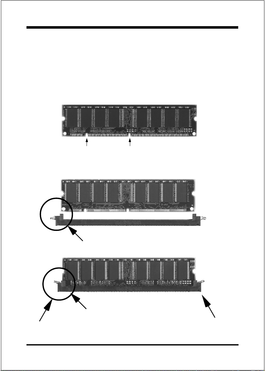
DIMM Module Installation
Figure 7 displays the notch marks and what they should look like on your DIMM
memory module.
DIMMs have 168-pins and two notches that will match with the onboard DIMM
socket. DIMM modules are installed by placing the chip firmly into the socket at a
90 degree angle and pressing straight down (figure 8) until it fits tightly into the
DIMM socket (figure 9).
LEFT KEY ZONE
(UNBUFFERED)
DIMM Module clip before installation
DIMM Module clip after installation
To remove the DIMM module simply press down both of the white clips on
either side and the module will be released from the socket.
CENTER KEY ZONE
(3.3 V DRAM)
Figure 7
Figure 8
Figure 9
Page 3-8
Page 21

Section 3-4
Device Connectors
InstallationEP-3VCA2
parallel port
PS/2 Mouse
PS/2
KEYBOARD
J2,J3: Chassis Panel Connector
Power LED, Speaker, Reset, Turbo LED, HDD LED, IR Conn., Sleep/
Power_ON
J4: CPU Fan Power
A plug-in for the CPU Fan Power
J6: Chassis Fan Power
A plug-in for the chassis Fan Power
J7: WOL (Wake On Lan) Connector
J8: WOM (Wake On Modem) Connector
USB port
COM1 COM2
Figure 10
Joystic/Midi port
Speaker
Line_in
MIC
IDE1: Primary IDE Connector
IDE2: Secondary IDE Connector
FDD1: Floppy Controller Connector
PW1: ATX Power Connector
20-pin power connector
CD1: CD Audio Connector
AUX1: AUX Audio Connector
Page 3-9
Page 22
Installation EP-3VCA2
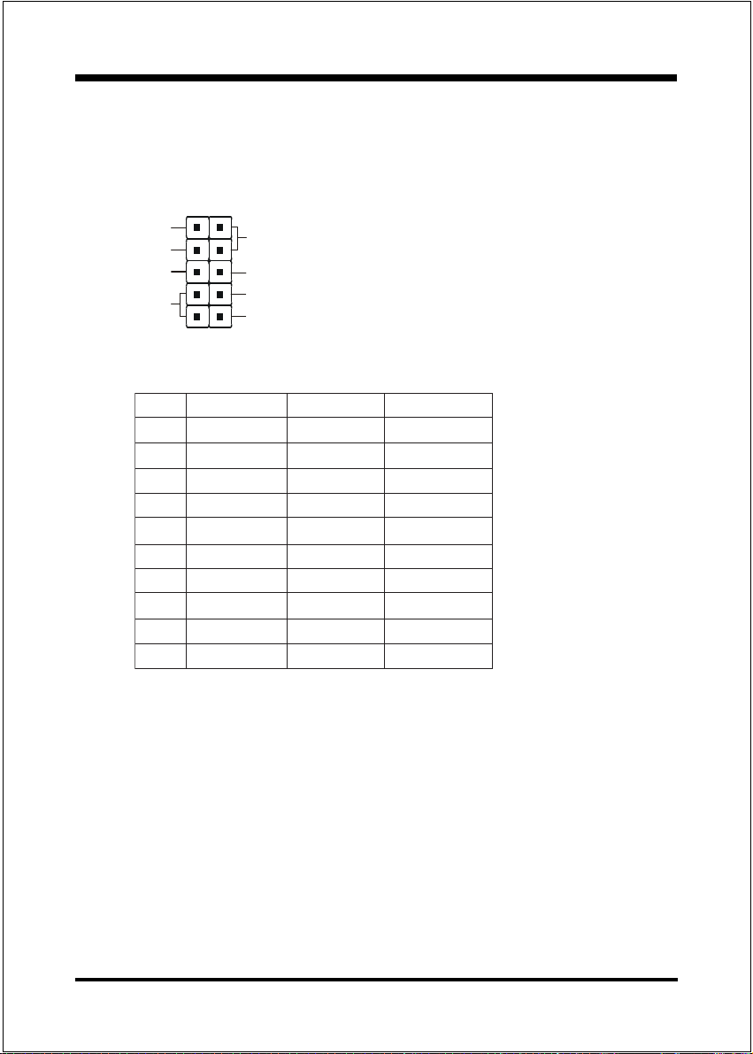
MODEM1: Telephony Connector
Pin1(Audio_in), Pin2/Pin3(GND), Pin4(Mic-out to Modem)
USB2: USB port header pins for adding two additional USB ports.
VCC
-Data
+Data
GND
1
5
6
GND
+Data
-Data
VCC
10
USB port header pin descriptions.
#NIProloceriWemaNlangiStnemmoC
1deRccVrewoPelbaC
2etihWataD-ataD
3neerGataD+ataD
4kcalBdnuorGdnuorGelbaC
5kcalBdnuorGdnuorGesaC
6kcalBdnuorGdnuorGesaC
7kcalBdnuorGdnuorGelbaC
8neerGataD+ataD
9etihWataD-ataD
01deRccVrewoPelbaC
Page 3-10
Page 23

Device Connectors (continued)
(This is connected to the power button on the case. Using the Soft-Off
by Pwr-BTTN feature, you can choose either Instant Off (turns system
off immediatly), or 4 sec delay (you need to hold the button down for
4 seconds before the system turns off). When the system is in 4 sec
delay mode, there is a special feature to make the system to go into
suspend mode when the button is pressed momentarily).
J3
+
+
Power On/Off
1
Turbo LED indicator - LED ON when higher speed is selected
IDE LED indicator - LED ON when Onboard PCI IDE Hard disks
is activate
IR Connector
1. VCC 4. GND
2. NC 5. IRTX
3. IRRX
1
InstallationEP-3VCA2
J2
Power LED - Power LED connector
1. Power LED(+) 4. NC
2. N/C 5. GND
3. GND
1
Speaker -
Connect to the system's speaker for beeping
1. Speaker 3. GND
2. N/C 4. GND
1
Reset - Closed to restart system.
1
Page 3-11
Page 24

Installation EP-3VCA2
Section 3-5
External Modem Ring-in Power
ON and Keyboard Power ON
Functions (KBPO)
On the basis of bounded functions in I/O chipset, the two serial ports are able to
support the External Modem Ring-in Power ON function. Once users connect the
external modem to COM1 or COM2, the EP-3VCA2 mainboard allows users to turn
on their system through the remote and host's dial-up control.
Exclusive Keyboard Power ON Function
To innovate a unique feature to benefit users, we devoted the easiest and most
convenient way to turn on your system based on the the ATX power supply.
How to work with it
Step 1: Please check JP4 at the position 2-3 after you finished the system
installation.
JP4 Keyboard Power-ON Function
1
JP4 = 1-2 Disabled (Default)
= 2-3 Enabled
Step 2: You can enjoy the Keyboard Power ON function (KBPO) by pressing any
key and BUTTON only to turn on your system. Your system will be turned
on automatically, after releasing the keys. To power off you system, you
can use the Soft-OFF function under Windows 95/98.
Notes: Intel ATX version 2.0 specification has recommended you use the power
supply with 0.72A(720mA) in 5.0VSB. With our EP-3VCA2 mainboard,
the 5.0VSB standby power only has to be > = 0.2A (200mA) then you can
enjoy this unique benefit. However, the ATX power supply which is < 0.
2 (200mA) is still applicable to your system by placed JP4 at the position
1-2 to disable this feature.
Page 3-12
Page 25

InstallationEP-3VCA2
3-6 STR (Suspend To RAM) Function
The EP-3VCA2 supports the STR power management state by maintaining the
appropriate states on the SDRAM interface signals. The power source must be
kept alive to the SDRAM during STR (ACPI S3). Advanced Configuration
Power Interface (ACPI) provides more Energy Saving Features for operating
systems that support OS such as Instant ON and QuickStartTM function.
1. To enable the ACPI function and use the STR functionally to save your system
energy, you are recommended to confirm the following requirements:
a. In BIOS, please select ACPI function: Enable and ACPI Suspend Type:
S3(STR) in the Power Management Setup menu.
b. Then, please type the following before installing the Windows® 98:
{Driver}:> Setup /p j
If the Windows® 98 installed in your system without the parameters above,
please do refer your manual or contact Microsoft for more detail and then
upgrade the system to support ACPI function.
c. Restart your system.
d. Getting in to the Advanced of the Power Management icon of Control
Panel, and selecting the Stand By in the Power Buttons.
2. Getting start with STR function, please click the START button and choose
Shut Down icon. Then, select the Stand By option in the Shut Down Windows
box to let system go to STR mode.
Here are the differences between STR power saving mode and Green (or
Suspend) mode:
a. It is the most advanced Power Management mode
b. It cuts all the power supplied to peripherals except to Memory - max. power
saving
Page 3-13
Page 26

Installation EP-3VCA2
c. It saves and keeps all on-screen data including any executed applications to
SDRAM.
d. You must push the Power button connected with onboard J3 pin to wake up
you system (not to click to mouse or press keyboard to wake up the system.)
Just pushing Power button, your system will quickly back to the last screen for
you.
The LED Indicator for ACPI Status table shown below will guide you and give
you a reference for ACPI status on this mainboard.
ACPI Onboards LED Status Indicator Table
Onboards
LED
Location
LED1
(Red LED)
J2
PW_LED
Status
Plug in the ATX
Power Core
Power ON
J3(PW-ON)
Green Mode
(S1)
STR
(S3)
OFF ON ON ON OFF
OFF ON Blinking OFF OFF
Shutdown
(Soft-OFF)
(S5)
Page 3-14
Page 27

EP-3VCA2
BIOS
Section 4
BIOS SETUP
Main Menu
Awards ROM BIOS provides a built-in Setup program which allows user to
modify the basic system configuration and hardware parameters. The modified
data will be stored in a battery-backed CMOS, so that data will be retained even
when the power is turned off. In general, the information saved in the CMOS
RAM will stay unchanged unless there is a configuration change in the system,
such as hard drive replacement or a device is added.
It is possible for the CMOS battery to fail, this will cause data loss in the CMOS
only. If this does happen you will need to reconfigure your BIOS settings.
To enter the Setup Program :
Power on the computer and press the <Del> key immediately, this will bring you
into the BIOS CMOS SETUP UTILITY.
Figure 1: CMOS Setup Utility
Page 4-1
Page 28

BIOS EP-3VCA2
The menu displays all the major selection items. Select the item you need to
reconfigure. The selection is made by moving the cursor (press any direction key
) to the item and pressing the Enter key. An on-line help message is displayed at
the bottom of the screen as the cursor is moved to various items which provides a
better understanding of each function. When a selection is made, the menu of the
selected item will appear so that the user can modify associated configuration
parameters.
4-1 Standard CMOS Setup
Choose Standard CMOS Setup in the CMOS SETUP UTILITY Menu (Figure 2).
The Standard CMOS Setup allows the user to configure system settings such as
the current date and time, type of hard disk drive installed, floppy drive type, and
display type. Memory size is auto-detected by the BIOS and displayed for your
reference. When a field is highlighted (use direction keys to move the cursor and
the <Enter> key to select), the entries in the field can be changed by pressing the
<PgDn> or the <PgUp> key.
Page 4-2
Figure 2: Standard CMOS Setup
Page 29

EP-3VCA2
NOTE: If the hard disk Primary Master/Slave and Secondary Master/
Slave are set to Auto, then the hard disk size and model will be auto-
detected.
NOTE: The Halt On: field is used to determine when to halt the system
by the BIOS if an error occurs.
NOTE: Floppy 3 Mode support is a mode used to support a special 3.5
drive used in Japan. This is a 3.5 disk that stores only 1.2 MB, the
default setting for this is disabled.
BIOS
4-2 Advanced BIOS Features
Selecting the BIOS FEATURES SETUP option in the CMOS SETUP UTILITY
menu allows users to change system related parameters in the displayed menu.
This menu shows all of the manufacturers default values for the EP-3VCA2.
Pressing the [F1] key will display a help message for the selected item.
Figure 3: BIOS Features Setup
Page 4-3
Page 30

BIOS EP-3VCA2
Virus Warning: During and after the system boots up, any attempt to write to the
boot sector or partition table of the hard disk drive will halt the system and an
error message will appear.
You should then run an anti-virus program to locate the virus. Keep in mind that
this feature protects only the boot sector, not the entire hard drive.
The default value is Disabled.
Enabled: Activates automatically when the system boots up causing a warning
message to appear when anything attempts to access the boot sector.
Disabled: No warning message will appear when anything attempts to access the
boot sector.
Note: Many disk diagnostic programs that access the boot sector table
can trigger the virus warning message. If you plan to run such a
program, we recommend that you first disable the virus warning.
CPU Internal Cache: This controls the status of the processors internal cache
area. The default is Enabled.
Enabled: This activates the processors internal cache thereby increasing
performance.
Disabled: This deactivates the processors internal cache thereby lowering
performance.
External (L2) Cache: This controls the status of the external (L2) cache area.
The default is Enabled.
Enabled: This activates the motherboards L2 cache thereby increasing
performance.
Disabled: This deactivates the motherboards L2 cache thereby lowering
performance.
CPU L2 Cache ECC Checking: This control if the CPUs L2 Cache will
support Error Checking and Correcting (ECC). The default is Disabled.
Enabled: Enables ECC support for the CPUs L2 cache. Performance will
decrease 2% ~ 4%.
Disabled: Disables ECC support for the CPUs L2 cache.
Processor Number Feature: Pentium III or later CPU new feature. The default
is Enabled.
Enabled: Processor serial number readable.
Disabled: Processor serial number disabled.
Page 4-4
Page 31

EP-3VCA2
Quick Power On Self Test: This category speeds up the Power On Self Test
(POST). The default is Enabled.
Enabled: This setting will shorten or skip of the items checked during POST.
Disabled: Normal POST.
First /Second/Third/Other Boot Device: The BIOS attempts to load the operat-
ing system from the devices in the sequence selected in these items.
The choice: Floppy, LS/ZIP, HDD, SCSI, CDROM, Disabled.
Swap Floppy Drive: This will swap your physical drive letters A & B if you are
using two floppy disks. The default is Disabled.
Enabled: Floppy A & B will be swapped under the O/S.
Disabled: Floppy A & B will be not swapped.
Boot Up Floppy Seek: During Power-On-Self-Test (POST), BIOS will deter-
mine if the floppy disk drive installed is 40 or 80 tracks. Only 360K type is 40
tracks while 760K, 1.2MB and 1.44MB are all 80 tracks. The default is Enabled.
Enabled: The BIOS will search the floppy disk drive to determine if it is 40 or
80 tracks.
Disabled: The BIOS will not search for the type of floppy disk drive by track
number.
Note: BIOS can not tell the difference between 720K, 1.2MB and 1.44MB
drive types as they are all 80 tracks.
BIOS
Boot Up NumLock Status: This controls the state of the NumLock key when the
system boots. The default is On.
On: The keypad acts as a 10-key pad.
Off: The keypad acts like the cursor keys.
Gate A20 Option: This refers to the way the system addresses memory above
1MB (extended memory). The default is Fast.
Normal: The A20 signal is controlled by the keyboard controller or chipset
hardware.
Fast: The A20 signal is controlled by Port 92 or chipset specific method.
Page 4-5
Page 32

BIOS EP-3VCA2
Typematic Rate Setting: This determines the keystrokes repeat rate.
The default is Disabled.
Enabled: Allows typematic rate and typematic delay programming.
Disabled: The typematic rate and typematic delay will be controlled by the
keyboard controller in your system.
Typematic Rate (Chars/Sec): This is the number of characters that will be
repeated by a keyboard press. The default is 6.
6: 6 characters per second. 8: 8 characters per second.
10: 10 characters per second. 12: 12 characters per second.
15: 15 characters per second. 20: 20 characters per second.
24: 24 characters per second. 30: 30 characters per second.
Typematic Delay (msec): This setting controls the time between the first and
the second character displayed by typematic auto-repeat. The default is 250.
250: 250 msec.
500: 500 msec.
750: 750 msec.
1000: 1000 msec.
Security Option: This category allows you to limit access to the System and
Setup, or just to Setup. The default is Setup.
System: The system will not boot and the access to Setup will be denied if the
correct password is not entered at the prompt.
Setup: The system will boot; but the access to Setup will be denied if the
incorrect password is not entered at the prompt.
OS Select For DRAM > 64MB: Some operating systems require special
handling. Use this option only if your system has greater than 64MB of memory.
The default is Non-OS2.
OS2: Select this if you are running the OS/2 operating system with greater
than 64MB of RAM.
Non-OS2: Select this for all other operating systems and configurations.
Video BIOS Shadow: This option allows video BIOS to be copied into RAM.
Video Shadowing will increase the video performance of your system.
The default is Enabled.
Page 4-6
Page 33

EP-3VCA2
Enabled: Video shadow is enabled.
Disabled: Video shadow is disabled.
C8000 - CBFFF Shadow:
CC000 - CFFFF Shadow:
D0000 - D3FFF Shadow:
D4000 - D7FFF Shadow:
D8000 - DBFFF Shadow:
DC000 - DFFFF Shadow:
These categories determine whether ROMs from option cards will be copied into
RAM. This will be in 16K byte or 32K byte units, and the size will depend on
chipset of the option card.
Enabled: Optional shadow is enabled.
Disabled: Optional shadow is disabled.
BIOS
Page 4-7
Page 34

BIOS EP-3VCA2
4-3 Advanced Chipset Fea tures
Choose the CHIPSET FEATURES SETUP in the CMOS SETUP UTILITY menu
to display following menu.
Figure 4: Chipset Features Setup
Bank 0/1, 2/3, 4/5 DRAM Timing: This value in this field is set by the system
board manufacturer, depending on whether the board has paged DRAMs or EDO
(extended data output) DRAMs.
The Choice: Bank 0/1, 2/3, 4/5.
SDRAM Cycle length: This setting defines the CAS timing parameter of the
SDRAM in terms of clocks. The default is 3.
2: Provides faster memory performance.
3: Provides better memory compatibility.
Bank Interleave: The item allows you to set how many banks of SDRAM support
in your mainboard.
The Choice: 2 Bank, 4 Bank, Disabled.
Page 4-8
Page 35

EP-3VCA2
DRAM Page-Mode: The item will active or inactive chipset page registers.
Enabled: Page-Mode Enabled.
Disabled: No page registers update and non Page-Mode operation.
Memory Hole : You can reserve this memory area for the use of ISA adaptor
ROMs. The default is Disabled.
Enabled: This field enables the main memory (15~16MB) to remap to ISA BUS.
Disabled:Normal Setting.
Note: If this feature is enabled you will not be able to cache this memory segment.
System BIOS Cacheable: This allows you to copy your BIOS code from slow
ROM to fast RAM. The default is Disabled.
Enabled: The option will improve system performance. However, if any program
writes to this memory area, a system error may result.
Disabled: System BIOS non-cacheable.
Video BIOS Cacheable: This option copies the video ROM BIOS to fast RAM
(C0000h to C7FFFh). The default is Disabled.
Enabled: Enables the Video BIOS Cacheable to speed up the VGA Performance.
Disabled: Will not use the Video BIOS Cacheable function.
BIOS
Video RAM Cacheable: This option allows the CPU to cache read/writes of the
video RAM. The default is Disabled.
Enabled: This option allows for faster video access.
Disabled: Reduced video performance.
AGP Aperture Size: The amount of system memory that the AGP card is
allowed to share. The default is 64.
4: 4MB of systems memory accessable by the AGP card.
8: 8MB of systems memory accessable by the AGP card.
16: 16MB of systems memory accessable by the AGP card.
32: 32MB of systems memory accessable by the AGP card.
64: 64MB of systems memory accessable by the AGP card.
128: 128MB of systems memory accessable by the AGP card.
256: 256MB of systems memory accessable by the AGP card.
Page 4-9
Page 36

BIOS EP-3VCA2
AGP-4X Mode: Chipset AGP Mode support.
Options: x1 , x2 and x4.
USB Keyboard Support: This controls the activation status of an optional USB
keyboard that may be attached. The default is disabled.
Enabled: Enable USB keyboard support.
Disabled: Disable USB keyboard support.
OnChip Sound: Turn on/off onchip sound device.
OnChip Modem: Turn on/off onchip software modem device.
CPU to PCI Write Buffer: When enabled, up to four D words of data can be
written to the PCI bus without interruting the CPU. When disabled, a write buffer
is not used and the CPU read cycle will not be completed until the PCI bus signals
that it is ready to receive the data.
The Choice: Enabled, Disabled.
PCI Dynamic Bursting: When Enabled, data transfers on the PCI bus, where
possible, make use of the high-performance PCI bust protocol, in which graeater
amounts of data are transferred at a single command.
The Choice: Enabled, Disabled.
PCI Master 0 WS Write: When Enabled, writes to the PCI bus are command
with zero wait states.
The Choice: Enabled, Disabled.
PCI Delay Transaction: The chipset has an embedded 32-bit posted write buffer
to support delay transactions cycles. Select Enabled to support compliance with
PCI specification version 2.1.
The Choice: Enabled, Disabled.
PCI #2 Access #1 Retry: This item allows you enabled/disable the PCI #2
Access #1 Retry.
The Choice: Enabled, Disabled.
Memory Parity/ECC Check: If the DRAM chip in your system support Parity/
ECC check, select Enabled.
Page 4-10
Page 37

EP-3VCA2
4-4 Integrated Peripherals
Figure 5: Integrated Peripherals
BIOS
Note: If you do not use the Onboard IDE connector, then you will need to
set Onboard Primary PCI IDE: Disabled and Onboard Secondary
PCI IDE: Disabled
Note: The Onboard PCI IDE cable should be equal to or less than 18
inches (45 cm.).
OnChip IDE Channel0: The default value is Enabled.
Enabled: Enables Onboard IDE primary port.
Disabled: Disables Onboard IDE primary port.
OnChip IDE Channel1: The default is Enabled.
Enabled: Enables Onboard IDE secondary port.
Disabled: Disables Onboard IDE secondary port.
IDE Prefetch Mode: Enable prefetching for IDE drive interfaces that support its
faster drive accesses. If uou are getting disk drive errors, change the setting to
omit the drive interface where the errors occur. Depending on the configuration
Page 4-11
Page 38

BIOS EP-3VCA2
of your IDE subsystem, this field may not appear, and it does not appear when the
Internal PCI/IDE field, above, is Disabled.
The Choice: Enabled, Disabled.
Primary Master PIO: The default is Auto.
Auto: BIOS will automatically detect the Onboard Primary Master PCI IDE
HDD Accessing mode.
Mode 0~4: Manually set the IDE Programmed interrupt mode.
Primary Slave PIO: The default is Auto.
Auto: BIOS will automatically detect the Onboard Primary Slave PCI IDE
HDD Accessing mode.
Mode 0~4: Manually set the IDE Programmed interrupt mode.
Secondary Master PIO: The default is Auto.
Auto: BIOS will automatically detect the Onboard Secondary Master PCI
IDE HDD Accessing mode.
Mode 0~4: Manually set the IDE Programmed interrupt mode.
Secondary Slave PIO: The default is Auto.
Auto: BIOS will automatically detect the Onboard Secondary Slave PCI
IDE HDD Accessing mode.
Mode 0~4: Manually set the IDE Programmed interrupt mode.
Primary Master UDMA: This allows you to select the mode of operation for
the hard drive. The default is Auto.
Auto: The computer will select the optimal setting.
Disabled: The hard drive will run in normal mode.
Primary Slave UDMA: This allows you to select the mode of operation for the
hard drive. The default is Auto.
Auto: The computer will select the optimal setting.
Disabled: The hard drive will run in normal mode.
Secondary Master UDMA: This allows you to select the mode of operation for
the hard drive. The default is Auto.
Auto: The computer will select the optimal setting.
Disabled: The hard drive will run in normal mode.
Page 4-12
Page 39

EP-3VCA2
Secondary Slave UDMA: This allows you to select the mode of operation for
the hard drive. The default is Auto.
Auto: The computer will select the optimal setting.
Disabled: The hard drive will run in normal mode.
Init Display First: If two video cards are used (1 AGP and 1 PCI) this specifies
which one will be the primary display adapter. The default is PCI Slot.
PCI Slots: PCI video card will be primary adapter.
AGP: AGP video card will be primary adapter.
IDE HDD Block Mode: IDE Block Mode allows the controller to access blocks
of sectors rather than a single sector at a time. The default is Enabled.
Enabled: Enabled IDE HDD Block Mode. Provides higher HDD transfer rates.
Disabled: Disable IDE HDD Block Mode.
Onboard FDD Controller: This controls the state of the onboard floppy
controller. The default value is Enabled.
Enabled: Enable the Onboard VIA686A Chipss floppy drive interface controller.
Disabled: Disable the Onboard VIA686A Chips floppy drive interface controller.
Onboard Serial Port 1: This field allows the user to configure the 1st serial
port. The default is Auto.
AUTO: Enable Onboard Serial port 1 and address is Auto adjusted.
COM1: Enable Onboard Serial port 1 and address is 3F8H/IRQ4.
COM2: Enable Onboard Serial port 1 and address is 2F8H/IRQ3.
COM3: Enable Onboard Serial port 1 and address is 3E8H/IRQ4.
COM4: Enable Onboard Serial port 1 and address is 2E8H/IRQ3.
Disabled: Disable Onboard SMC CHIPs Serial port 1.
BIOS
Onboard Serial Port 2: This field allows the user to configure the 2nd serial port.
The default is Auto.
AUTO: Enable Onboard Serial port 2 and address is Auto adjusted.
COM1: Enable Onboard Serial port 2 and address is Auto.
COM2: Enable Onboard Serial port 2 and address is 2F8H/IRQ3.
COM3: Enable Onboard Serial port 2 and address is 3E8H/IRQ4.
COM4: Enable Onboard Serial port 2 and address is 2E8H/IRQ3.
Disabled: Disable Onboard SMC CHIPs Serial port 2.
Page 4-13
Page 40

BIOS EP-3VCA2
UART 2 Mode: This item allows you to determine which Infra Red (IR) function
of onboard I/O chip.
The Choice: Standard, ASKIR, HPSIR.
IR Function Duplex: This item allows you to select the IR function when you
select the UART2 Mode is ASKIR.
The Choice: Half, Full.
TX, RX inverting enable: This item invert serial port 2 TX and RX output signal
level.
No, No TX, RX have no signal inverting.
No, Yes RX have signal inverting.
Yes, No TX have signal inverting.
Yes, Yes TX, RX have signal inverting.
Onboard Parallel port: This field allows the user to configure the LPT port.
The default is 378H / IRQ7.
378H: Enable Onboard LPT port and address is 378H and IRQ7.
278H: Enable Onboard LPT port and address is 278H and IRQ5.
3BCH: Enable Onboard LPT port and address is 3BCH and IRQ7.
Disabled: Disable Onboard Winbond Chips LPT port.
Onboard Parallel Mode: This field allows the user to select the parallel port mode.
The default is ECP/EPP.
Normal: Standard mode. IBM PC/AT Compatible bidirectional parallel port.
EPP: Enhanced Parallel Port mode.
ECP: Extended Capabilities Port mode.
EPP+ECP: ECP Mode & EPP Mode.
ECP Mode USE DMA: This field allows the user to select DMA1 or DMA3 for
the ECP mode. The default is DMA3.
DMA1: This field selects the routing of DMA1 for the ECP mode.
DMA3: This field selects the routing of DMA3 for the ECP mode.
Parallel Port EPP Type: This item allows you to determine the IR transfer
mode of onboard I/O chip.
The Choice: EPP1.9, EPP1.7.
Page 4-14
Page 41

EP-3VCA2
Onboard Legacy Audio: Legacy Audio enabled/disabled.
Sound Blaster: Sound Blaster compatible device enabled/disabled.
SB I/O Base Address: Sound Blaster I/O resource selection.
SB IRQ Select: Legacy audio device IRQ selection.
SB DMA Select: Sound Blaster DMA channel selection.
MPU-401: MPU-401 function enabled/disabled.
MPU-401 I/O Address: Built-in MPU-401 compatible MIDI I/O port selection:
300-303H
310-313H
320-323H
330-333H (default)
Game Port (200-207H): Built-in joystick port support disabled/enabled(default).
BIOS
Page 4-15
Page 42

BIOS EP-3VCA2
4-5 Pow er Management Setup
Choose the POWER MANAGEMENT SETUP in the CMOS SETUP UTILITY to
display the following screen. This menu allows the user to modify the power
management parameters and IRQ signals. In general, these parameters should not
be changed unless its absolutely necessary.
Figure 6: Power Management Setup
ACPI Function: This option allows you to select ACPI Function.
The default is Enabled.
Enabled: Support ACPI function for new O.S
Disabled: No Support ACPI function.
You can only change the content of Doze Mode, Standby Mode, and Suspend
Mode when the Power Management is set to User Define.
Power Management: Use this to select your Power Management selection.
The default is User define.
Disabled: The system operates in NORMAL conditions (Non-GREEN), and
the Power Management function is disabled.
Max. saving: Maximum power savings. Inactivity period is 1 minute in each mode.
Page 4-16
Page 43

EP-3VCA2
Min. saving: Minimum power savings. Inactivity period is 1 hour in each mode.
User define: Allows user to define PM Timers parameters to control power
saving mode.
ACPI Suspend Type: This item allows you to select S1(POS) or S3(STR) function.
The choice: S1(POS), S3(STR).
PM controlled APM: This option shows weather or not you want the Power
Management to be controlled the Advanced Power Management (APM).
The default is Yes.
Ye s: APM controls your PM
No: APM does not control your PM
Video Off Option: Tells you what time frame that the video will be disabled
under current power management settings. The default is Standby.
Standby: Video powers off after time shown in standby mode setting.
Doze: Video powers off after time shown in doze mode setting.
Suspend: Video powers off after time shown in suspend mode setting.
N/A: Video power off not controlled by power management.
Video Off Method: This option allows you to select how the video will be
disabled by the power management. The default is V/H Sync + Blank
V/H Sync + Blank: System turns off vertical and horizontal synchronization
ports and writes blanks to the video buffer.
DPMS: Select this option if your monitor supports the Display
Power Management Signaling (DPMS) standard of the
Video Electronics Standards Association (VESA). Use the
software supplied for your video subsystem to select video
power management values.
Blank Screen: System only writes blanks to the video buffer.
BIOS
MODEM Use IRQ: Name the interrupt request (IRQ) line assigned to the
modem (if any) on your system. Activity of the selected IRQ always awakens the
system. Default is IRQ 3.
N/A: No IRQ is used. 3: IRQ 3
4: IRQ 4 5: IRQ 5
7: IRQ 7 9: IRQ 9
10: IRQ 10 11: IRQ 11
Page 4-17
Page 44

BIOS EP-3VCA2
Soft-Off by PWRBTN: Use this to select your soft-off function.
The default is Instant Off.
Instant Off: Turns off the system instantly.
Delay 4 Second : Turns off the system after a 4 second delay. If momentary
press of button, the system will go into Suspend Mode. Press
the power botton again to take system out of Suspend Mode.
State After Power Failure: This field lets you determine the state that your PC
returns to after a power failure. If set to Off, the PC will not boot after a power
failure, if set to On, the PC will restart after a power failure.
CPU FAN In Suspend: This option is used to set if the CPU fans will turn off
during suspend mode. The default is Off.
On: The system will turn off the CPU fans during suspend mode.
Off: The system will not turn off the CPU fan during suspend mode.
VGA: When set to On (default), any event occurring at a VGA port will awaken a
system which has been powered down.
LPT & COM: When set to On (default), any event occurring at a COM(serial)/
LPT (printer) port will awaken a system which has been powered down.
HDD & FDD: When set to On (default), any event occurring at a hard or floppy
drive port will awaken a system which has been powered down.
PCI Card: When set to On (default), any event occurring to the DMA controller
will awaken a system which has been powered down.
Modem Ring Resume: When set to Enabled, any event occurring to the Modem
Ring will awaken a system which has been powered down.
RTC Alarm Resume: When set to Enable rtc alarm resume, you could set the
date (of month) and timer (hh:mm:ss), any event occurring at will awaken a
system which has been powered down.
Primary INTR: When set to On (default), any event occurring at will awaken a
system which has been powered down.
Page 4-18
Page 45

EP-3VCA2
BIOS
4-6 PNP/PCI Configuration
The PNP/PCI configuration program is for the user to modify the PCI/ISA IRQ
signals when various PCI/ISA cards are inserted in the PCI or ISA slots.
WARNING: Conflicting IRQs may cause the system to not find certain devices.
Figure 7: PCI Configuration Setup
PNP OS Installed: Do you have a PNP OS installed on your system. The default is
No.
Ye s : Select if you are using a PNP OS.
No: Select if your OS does not support PNP.
Reset Configuration Data: This setting allows you to clear ESCD data.
The default is Disabled
Disabled: Normal Setting.
Enabled: If you have plugged in some Legacy cards to the system and they were
recorded into ESCD (Extended System Configuration Data), you can
set this field to Enabled in order to clear ESCD.
Page 4-19
Page 46

BIOS EP-3VCA2
Resources Controlled By: Who controlled the system PNP/PCI resources.
The default is Auto.
Manual: PNP Cards resources will be controlled manually. You can set which
IRQ-X and DMA-X are assigned to PCI/ISA PNP or Legacy ISA Cards.
Auto: If your ISA card and PCI card are all PNP cards, BIOS will assign the
interrupt resource automatically.
PCI/VGA Palette Snoop: Leave this field at Disabled.
The choice: Enabled, Disabled.
Assign IRQ For USB: This item allows BIOS to assign whether IRQ is with USB or
not. If you have not connect the USB device. Can release the IRQ for other device.
The default is Enabled.
Enabled: Provides IRQ for USB device.
Disabled: Release IRQ for other device.
Slot 1 to Slot 5 Use IRQ No: These settings allow the user to specify what IRQ will
be assigned to PCI devices in the chosen slot. Options available: Auto,3,4,5,7,9,10,
11,12,14 & 15. The defaults are Auto.
Page 4-20
Page 47

EP-3VCA2
BIOS
4-7 PC Health Status
31oC/87oF
0oC/32oF
6135 RPM
0 RPM
1.62V
1.5V
3.22V
5.01V
12.12V
Current CPU Temperature: This is the current temperature of the CPU.
Current System Temperature: This is the Current temperature of the system.
Current CPU FAN Speed: The current CPU fan speed in RPMs.
Current Chassis FAN Speed: The current chassis fan speed in RPMs.
CPU(V): The voltage level of the CPU(Vcore/Vtt).
3.3V, 5V, 12V: The voltage level of the switch power supply.
Page 4-21
Page 48

BIOS EP-3VCA2
4-8 Frequency/V oltage Control
Default
DRAM Clock : The item will synchronize/asynchronize DRAM operation clock.
Host Clock: DRAM has same working clock with CPU host bus.
2/3 Host: DRAM running with lower operation clock.
Auto Detect DIMM/PCI Clk: When enabled the motherboard will automatically
disable the clock source for a DIMM socket which does not have a module in it.
Same applies for PCI slots. The default is Enabled.
Enabled: Enables this option.
Disabled: Disables this option.
Spread Spectrum Modulated: The default is Disabled.
Enabled: Enables this option.
Disabled: Disables this option.
CPU Host Clock : Allows the external clock to be modified depending upon
what FSB has been selected. Should not be used to clock processor faster than it
was designed for. The default is Default.
Page 4-22
Page 49

EP-3VCA2
CPU/PCI Clk Ratio : The default is Auto.
CPU Ratio : This item allows you to select the CPU ratio.
BIOS
4-9 Defaults Menu
Selecting Defaults from the main menu shows you two options which are described
below
Load Fail-Safe Defaults
When you press <Enter> on this item you get a confirmation dialog box with a
message similar to:
Load Fail-Safe Defaults (Y/N) ? N
Pressing Y loads the BIOS default values for the most stable, minimal-performance system operations.
Load Optimized Defaults
When you press <Enter> on this item you get a confirmation dialog box with a
message similar to:
Load Optimized Defaults (Y/N) ? N
Pressing Y loads the default values that are factory settings for optimal performance system operations.
Page 4-23
Page 50

BIOS EP-3VCA2
4-10 Supervisor/User Password Setting
You can set either supervisor or user password, or both of then. The differences
between are:
supervisor password : can enter and change the options of the setup menus.
user password : just can only enter but do not have the right to change the
options of the setup menus. When you select this function, the following message
will appear at the center of the screen to assist you in creating a password.
ENTER PASSWORD:
Type the password, up to eight characters in length, and press <Enter>. The password typed now will clear any previously entered password from CMOS memory.
You will be asked to confirm the password. Type the password again and press
<Enter>. You may also press <Esc> to abort the selection and not enter a password.
To disable a password, just press <Enter> when you are prompted to enter the
password. A message will confirm the password will be disabled. Once the password is disabled, the system will boot and you can enter Setup freely.
PASSWORD DISABLED.
When a password has been enabled, you will be prompted to enter it every time you
try to enter Setup. This prevents an unauthorized person from changing any part of
your system configuration.
Additionally, when a password is enabled, you can also require the BIOS to request
a password every time your system is rebooted. This would prevent unauthorized
use of your computer.
You determine when the password is required within the BIOS Features Setup Menu
and its Security option (see Section 3). If the Security option is set to System, the
password will be required both at boot and at entry to Setup. If set to Setup,
prompting only occurs when trying to enter Setup.
Page 4-24
Page 51

EP-3VCA2
BIOS
4-11 Exit Selecting
Save & Exit Setup
Pressing <Enter> on this item asks for confirmation:
Save to CMOS and EXIT (Y/N)? Y
Pressing Y stores the selections made in the menus in CMOS a special section
of memory that stays on after you turn your system off. The next time you boot
your computer, the BIOS configures your system according to the Setup selections stored in CMOS. After saving the values the system is restarted again.
Exit Without Saving
Pressing <Enter> on this item asks for confirmation:
Quit without saving (Y/N)? Y
This allows you to exit Setup without storing in CMOS any change. The previous
selections remain in effect. This exits the Setup utility and restarts your computer.
Page 4-25
Page 52

BIOS EP-3VCA2
Page Left Blank
Page 4-26
Page 53

AppendixEP-3VCA2
Appendix A
A-1 MEMORY MAP
Address Range Size Description
[00000-7FFFF] 512K Conventional memory
[80000-9FBFF] 127K Extended Conventional memory
[9FC00-9FFFF] 1K Extended BIOS data area if PS/2 mouse is
installed
[A0000-C7FFF] 160K Available for Hi DOS memory
[C8000-DFFFF] 96K Available for Hi DOS memory and adapter
ROMs
[E0000-EEFFF] 60K Available for UMB
[EF000-EFFFF] 4K Video service routine for Monochrome &
CGA adaptor
[F0000-F7FFF] 32K BIOS CMOS setup utility
[F8000-FCFFF] 20K BIOS runtime service routine (2)
[FD000-FDFFF] 4K Plug and Play ESCD data area
[FE000-FFFFF] 8K BIOS runtime service routine (1)
A-2 I/O MAP
[000-01F] DMA controller.(Master)
[020-021] INTERRUPT CONTROLLER.(Master)
[022-023] CHIPSET control registers. I/O ports.
[040-05F] TIMER control registers.
[060-06F] KEYBOARD interface controller.(8042)
[070-07F] RTC ports & CMOS I/O ports.
[080-09F] DMA register.
[0A0-0BF] INTERRUPT controller.(Slave)
[0C0-0DF] DMA controller.(Slave)
[0F0-0FF] MATH COPROCESSOR.
[1F0-1F8 ] HARD DISK controller.
[278-27F] PARALLEL port 2.
[2B0-2DF] GRAPHICS adapter controller.
A-1
Page 54

Appendix EP-3VCA2
[2F8-2FF] SERIAL port 2.
[360-36F] NETWORK ports.
[378-37F] PARALLEL port 1.
[3B0-3BF] MONOCHROME & PARALLEL port adapter.
[3C0-3CF] EGA adapter.
[3D0-3DF] CGA adapter.
[3F0-3F7] FLOPPY DISK controller.
[3F8-3FF] SERIAL port 1.
A-3 TIMER & DMA CHANNELS MAP
TIMER MAP:
TIMER Channel 0 System timer interrupt.
TIMER Channel 1 DRAM REFRESH request.
TIMER Channel 2 SPEAKER tone generator.
DMA CHANNELS:
DMA Channel 0 Available.
DMA Channel 1 Onboard ECP (Option).
DMA Channel 2 FLOPPY DISK (SMC CHIP).
DMA Channel 3 Onboard ECP (default).
DMA Channel 4 Cascade for DMA controller 1.
DMA Channel 5 Available.
DMA Channel 6 Available.
DMA Channel 7 Available
A-4 INTERRUPT MAP
NMI :
Parity check error.
IRQ (H/W):
0 System TIMER interrupt from TIMER 0.
1 KEYBOARD output buffer full.
2 Cascade for IRQ 8-15.
3 SERIAL port 2.
4 SERIAL port 1.
5 PARALLEL port 2.
A-2
Page 55

6 FLOPPY DISK (SMC CHIP).
7 PARALLEL port 1.
8 RTC clock.
9 Available.
10 Available.
11 Available.
12 PS/2 Mouse.
13 MATH coprocessor.
14 Onboard HARD DISK (IDE1) channel.
15 Onboard HARD DISK (IDE1) channel.
A-5 RTC & CMOS RAM MAP
RTC & CMOS:
00 Seconds.
01 Second alarm.
02 Minutes.
03 Minutes alarm.
04 Hours.
05 Hours alarm.
06 Day of week.
07 Day of month.
08 Month.
09 Year.
0A Status register A.
0B Status register B.
0C Status register C.
0D Status register D.
0E Diagnostic status byte.
0F Shutdown byte.
10 FLOPPY DISK drive type byte.
11 Reserve.
12 HARD DISK type byte.
13 Reserve.
14 Equipment type.
15 Base memory low byte.
AppendixEP-3VCA2
A-3
Page 56

Appendix EP-3VCA2
16 Base memory high byte.
17 Extension memory low byte.
18 Extension memory high byte.
19-2d
2E-2F
30 Reserved for extension memory low byte.
31 Reserved for extension memory high byte.
32 DATE CENTURY byte.
33 INFORMATION FLAG.
34-3F Reserve.
40-7F Reserved for CHIPSET SETTING DATA.
A-4
Page 57

AppendixEP-3VCA2
Appendix B
B-1 POST CODES
ISA POST codes are typically output to I/O port address 80h.
POST (hex) DESCRIPTION
01-02 Reserved.
C0 Turn off OEM specific cache, shadow.
03 1. Initialize EISA registers (EISA BIOS only).
2. Initialize all the standard devices with default values
Standard devices includes.
- DMA controller (8237).
- Programmable Interrupt Controller (8259).
- Programmable Interval Timer (8254).
- RTC chip.
04 Reserved
05 1. Keyboard Controller Self-Test.
06 2. Enable Keyboard Interface.
07 Reserved.
08 Verifies CMOS's basic R/W functionality.
C1 Auto-detection of onboard DRAM & Cache.
C5 Copy the BIOS from ROM into E0000-FFFFF shadow RAM
so that POST will go faster.
08 Test the first 256K DRAM.
09 OEM specific cache initialization. (if needed)
0A 1. Initialize the first 32 interrupt vectors with correspond
ing Interrupt handlers. Initialize INT numbers from 33-120
with Dummy (Spurious) Interrupt Handler.
2. Issue CPUID instruction to identify CPU type.
3. Early Power Management initialization. (OEM specific)
0B 1. Verify the RTC time is valid or not.
2. Detect bad battery.
3. Read CMOS data into BIOS stack area.
4. PnP initializations including. (PnP BIOS only)
- Assign CSN to PnP ISA card.
A-5
Page 58

Appendix EP-3VCA2
- Create resource map from ESCD.
5. Assign IO & Memory for PCI devices. (PCI BIOS only)
0C Initialization of the BIOS Data Area. (40:ON - 40:FF)
0D 1. Program some of the Chipset's value according to Setup.
(Early Setup Value Program)
2. Measure CPU speed for display & decide the system
clock speed.
3. Video initialization including Monochrome, CGA, EGA/
VGA. If no display device found, the speaker will beep.
0E 1. Test video RAM. (If Monochrome display device found)
2. Show messages including.
- Award Logo, Copyright string, BIOS Data code & Part
No.
- OEM specific sign on messages.
- Energy Star Logo. (Green BIOS ONLY)
- CPU brand, type & speed.
- Test system BIOS checksum. (Non-Compress Version
only)
0F DMA channel 0 test.
10 DMA channel 1 test.
11 DMA page registers test.
12-13 Reserved.
14 Test 8254 Timer 0 Counter 2.
15 Test 8259 interrupt mask bits for channel 1.
16 Test 8259 interrupt mask bits for channel 2.
17 Reserved.
19 Test 8259 functionality.
1A-1D Reserved.
1E If EISA NVM checksum is good, execute EISA initialization.
(EISA BIOS only)
1F-29 Reserved.
30 Detect Base Memory & Extended Memory Size.
31 1. Test Base Memory from 256K to 640K.
2. Test Extended Memory from 1M to the top of memory.
32 1. Display the Award Plug & Play BIOS Extension message.
(PnP BIOS only)
A-6
Page 59

AppendixEP-3VCA2
2. Program all onboard super I/O chips (if any) including
COM ports, LPT ports, FDD port ... according to setup value.
33-3B Reserved.
3C Set flag to allow users to enter CMOS Setup Utility.
3D 1. Initialize Keyboard.
2. Install PS2 mouse.
3E Try to turn on Level 2 cache.
Note: Some chipset may need to turn on the L2 cache in
this stage.
But usually, the cache is turn on later in POST 61h.
3F-40 Reserved.
BF 1. Program the rest of the Chipset's value according to Setup.
(Later Setup Value Program)
41 2. If auto-configuration is enabled, program the chipset with
pre-defined Values.
42 Initialize floppy disk drive controller.
43 Initialize Hard drive controller.
45 If it is a PnP BIOS, initialize serial & parallel ports.
44 Reserved.
45 Initialize math coprocessor.
46-4D Reserved.
4E If there is any error detected (such as video, kb...), show all
error messages on the screen & wait for user to press <F1>
key.
4F 1. If password is needed, ask for password.
2. Clear the Energy Star Logo. (Green BIOS only)
50 Write all CMOS values currently in the BIOS stack area
back into the CMOS.
51 Reserved.
52 1. Initialize all ISA ROMs.
2. Later PCI initializations. (PCI BIOS only)
- assign IRQ to PCI devices.
- initialize all PCI ROMs.
3. PnP Initialzations. (PnP BIOS only)
- assign IO, Memory, IRQ & DMA to PnP ISA devices.
- initialize all PnP ISA ROMs.
4. Program shadows RAM according to Setup settings.
A-7
Page 60

Appendix EP-3VCA2
5. Program parity according to Setup setting.
6. Power Management Initialization.
- Enable/Disable global PM.
- APM interface initialization.
53 1. If it is NOT a PnP BIOS, initialize serial & parallel ports.
2. Initialize time value in BIOS data area by translate the
RTC time value into a timer tick value.
60 Setup Virus Protection. (Boot Sector Protection) function
ality
according to Setup setting.
61 1. Try to turn on Level 2 cache.
Note: If L2 cache is already turned on in POST 3D, this
part will be skipped.
2. Set the boot up speed according to Setup setting.
3. Last chance for Chipset initialization.
4. Last chance for Power Management initialization.
(Green BIOS only)
5. Show the system configuration table.
62 1. Setup daylight saving according to Setup value.
2. Program the NUM Lock, typematic rate & typematic
sp eed according to Setup setting.
63 1. If there is any changes in the hardware configuration,
update the ESCD information. (PnP BIOS only)
2. Clear memory that have been used.
3. Boot system via INT 19H.
FF System Booting. This means that the BIOS already pass the
control right to the operating system.
B-2 Unexpected Errors:
POST (hex) DESCRIPTION
B0 If interrupt occurs in protected mode.
B1 Unclaimed NMI occurs.0
A-8
Page 61

AppendixEP-3VCA2
Appendix C
NOTE:
The "LOAD SETUP DEFAULTS" function loads the system default data directly
from ROM and initializes the associated hardware properly. This function will be
necessary when you accept this mainboard, or the system CMOS data is corrupted.
CMOS Setup Utility - Copyright ( C ) 1984-1998
Standard CMOS Feature
Advanced BIOS Feature
Advanced Chipset Feature
Integrated Peripherals
Power Management Setup
PnP/PCI Configurations
PC Health Status
Esc : Quit ↑ ↓ ← → : Select Item
F10 : Save & Exit Setup
Load Optimized Defaults (Y/N)? Y
Time, Date, Hard Disk Type.
Frequency/Voltage Control
Load Fail-Safe Defaults
Load Optimized Defaults
Set Supervisor Password
Set User Password
Save & Exit Setup
Exit Without Saving
LOAD Optimized DEFAULTS
A-9
Page 62

Appendix EP-3VCA2
Page Left Blank
A-10
Page 63

AppendixEP-3VCA2
Appendix D
D-1 GHOST 5.1 Quick User’s Guide
Installation is very easy. You only need to copy the Ghost5 folder or
Ghost.exe to your hard disk.
The current market version is for single Client, so the LPT and NetBios
portions will not be explained further.
Description of Menus
Ghost clones and backs up Disk and Partition.
In which Disk indicates hard disk options
Partition indicates partition options
Check indicates check options
Disk
A-11
Page 64

Appendix EP-3VCA2
There are 3 hard disk functions:
1. Disk To Disk (disk cloning)
2. Disk To Image (disk backup)
3. Disk From Image (restore backup)
Important!
1. To use this function, the system must have at least 2 disks. Press the
Tab key to move the cursor.
2. When restoring to a destination disk, all data in that disk will be
completely destroyed.
Disk To Disk (Disk Cloning)
1. Select the location of the Source drive.
2. Select the location of the Destination drive.
3. When cloning a disk or restoring the backup, set the required partition
size as shown in the following figure.
A-12
Page 65

AppendixEP-3VCA2
4. Click OK to display the following confirmation screen. Select Yes to
start.
Disk To Image (Disk Backup)
1. Select the location of the Source drive.
2. Select the location for storing the backup file.
A-13
Page 66

Appendix EP-3VCA2
3. Click OK to display the following confirmation screen. Select Yes to
start.
Disk From Image (Restore Backup)
1. Select the Restore file.
2. Select the Destination drive of the disk to be restored.
A-14
Page 67

AppendixEP-3VCA2
3. When restoring disk backup, set the required partition size as shown in
the following figure.
4. Click OK to display the following confirmation screen. Select Yes to
start.
Partition
A-15
Page 68

Appendix EP-3VCA2
There are 3 partition functions:
1. Partition To Partition (partition cloning)
2. Partition To Image (partition backup)
3. Partition From Image (restore partition)
Partition To Partition (Partition Cloning)
The basic unit for partition cloning is a partition. Refer to disk cloning for
the operation method.
Partition To Image (Partition Backup)
1. Select the disk to be backed up.
2. Select the first partition to be backed up. This is usually where the
operating system and programs are stored.
A-16
Page 69

3. Select the path and file name for storing the backup file.
4. Is the file compressed? There are 3 options:
(1)No: do not compress data during backup
(2)Fast: Small volume compression
AppendixEP-3VCA2
(3)High: high ratio compression. File can be compressed to its minimum,
but this requires longer execution time.
5. During confirmation, select Yes to start performing backup.
A-17
Page 70

Appendix EP-3VCA2
Partition From Image (Restore Partition)
1. Select the backup file to be restored.
2. Select the source partition.
3. Select the disk to be restored.
A-18
Page 71

4. Select the partition to be restored.
5. Select Yes to start restoring.
AppendixEP-3VCA2
Check
This function checks the hard disk or backup file for backup or
restoration error due to FAT or track error.
A-19
 Loading...