

Page 1

TRADEMARK
All products and company names are trademarks or
registered trademarks of their respective holders.
These specifications are subject to change without
notice.
Manual Revision 3.0
September 23, 1999
S7-530AS7-530A
S7-530AS7-530A
S7-530A
ISA/PCI AGP Mainboard with OnboardISA/PCI AGP Mainboard with Onboard
ISA/PCI AGP Mainboard with OnboardISA/PCI AGP Mainboard with Onboard
ISA/PCI AGP Mainboard with Onboard
PCI IDE and Super Multi-I/OPCI IDE and Super Multi-I/O
PCI IDE and Super Multi-I/OPCI IDE and Super Multi-I/O
PCI IDE and Super Multi-I/O
Page 2

S7-530A
Table of Contents
Section 1 Introduction
Components Checklist .................................... 1-1
Overview
Power-On/Off (Remote)................................. 1-2
System Block Diagram ................................... 1-3
Section 2 Features
S7-530A Features.......................................... 2-1
Section 3 Installation
S7-530A Detailed Layout............................... 3-2
Easy Installation Procedure
Configure Jumpers .......................................... 3-3
System Memory Configuration ........................ 3-4
Device Connectors ......................................... 3-7
Section 4 Award BIOS Setup
BIOS Instructions ........................................... 4-1
Standard CMOS Setup .................................. 4-2
BIOS Features Setup ..................................... 4-3
Chipset Features Setup ................................... 4-8
Power Management Setup .............................. 4-12
PNP/PCI Configuration .................................. 4-17
Load Setup Defaults ....................................... 4-19
Integrated Peripherals ..................................... 4-18
Change Supervisor or User Password ............. 4-23
IDE HDD Auto Detection............................... 4-24
Save & Exit Setup .......................................... 4-26
Exit Without Saving......................................... 4-26
Page 3

S7-530A
Appendix
Appendix A
Memory Map ................................................. A-1
I/O Map......................................................... A-1
Timer & DMA Channels Map......................... A-2
Interrupt Map ................................................. A-2
R TC & CMOS RAM Map ............................ A-3
Appendix B
POST Codes ................................................. A-5
Unexpected Errors ......................................... A-8
Appendix C
Load Setup Defaults ....................................... A-9
Page 4

S7-530A
Page 5

IntroductionS7-530A
Page 1-1
Section 1
INTRODUCTION
Components Checklist
üü
üü
ü A. (1) One mainboard
üü
üü
ü B. (1) One user’s manual
üü
üü
ü C. (1) Floppy ribbon cable
üü
üü
ü D. (1) IDE ribbon cables
E. (2) PS/2 to AT keyboard connector adapter (optional)
üü
üü
ü F. (1) Ultra_DMA IDE driver diskette
(1) AGP Drivers
USERS
MANUAL
S7-530A
B
A
E
C
D
F
or
Page 6
Introduction S7-530A
Page 1-2
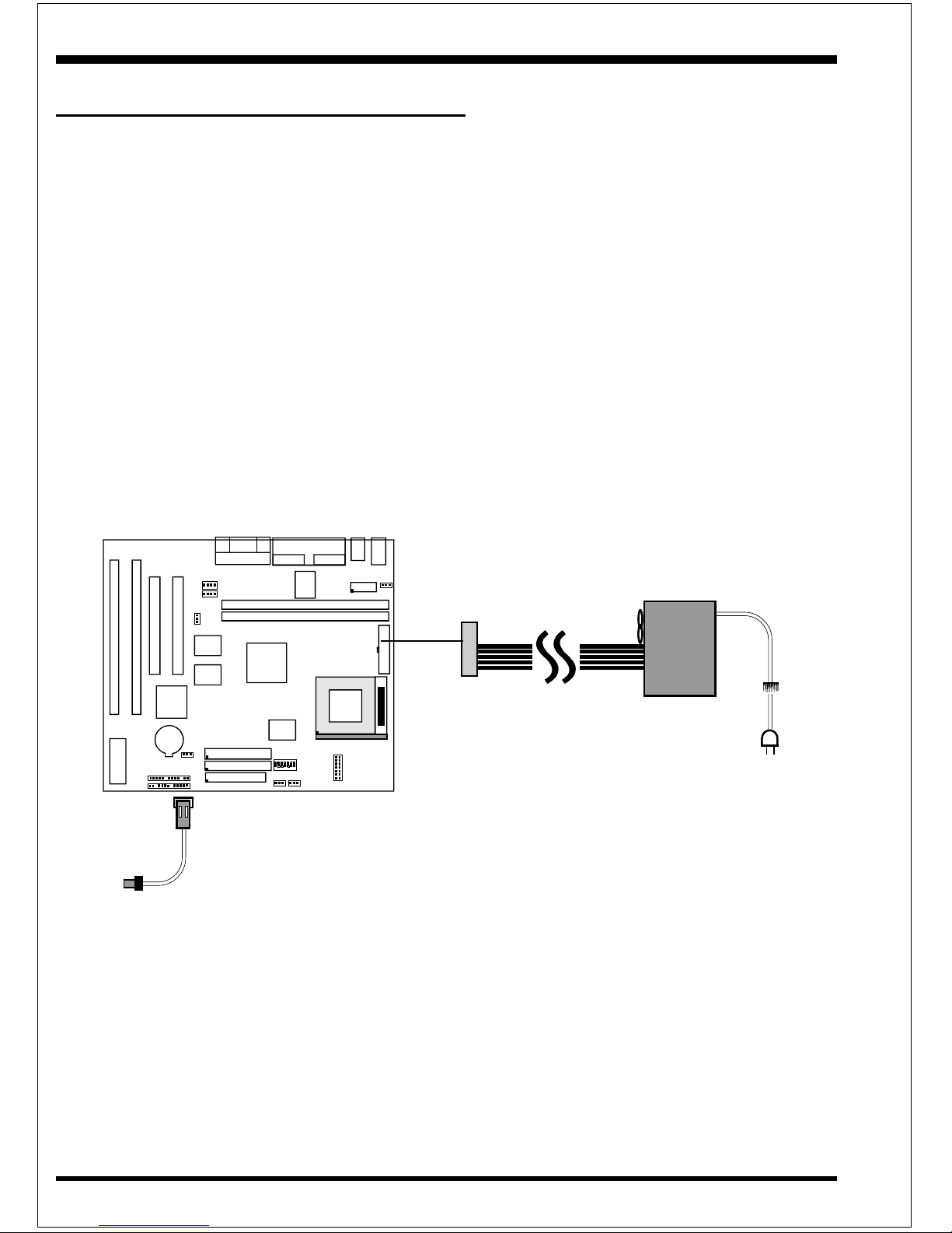
ATX
POWER SUPPLY
S7-530A Board
Power-On/Off (Remote)
The S7-530A has a single 20-pin connector for ATX power supplies. For ATX
power supplies that support the Remote On/Off feature, this should be connected to
the systems front panel for system Power On/Off button. The systems power On/
Off button should be a momentary button that is normally open.
The S7-530A has been designed with “Soft Off" functions. You can turn Off the
system from one of two sources: The first is the front panel Power On/Off button,
and the other is the "Soft Off" function (coming from the S7-530A’ s onboard circuit
controller) that can be controlled by the operating system. Windows 95/98 will
control this when the user clicks that they are ready to Shutdown the system.
Case (chassis) Power
ON/OFF button
Figure 4: Simple ATX Power
ON/OFF Controller
J3
Page 7
IntroductionS7-530A
Page 1-3
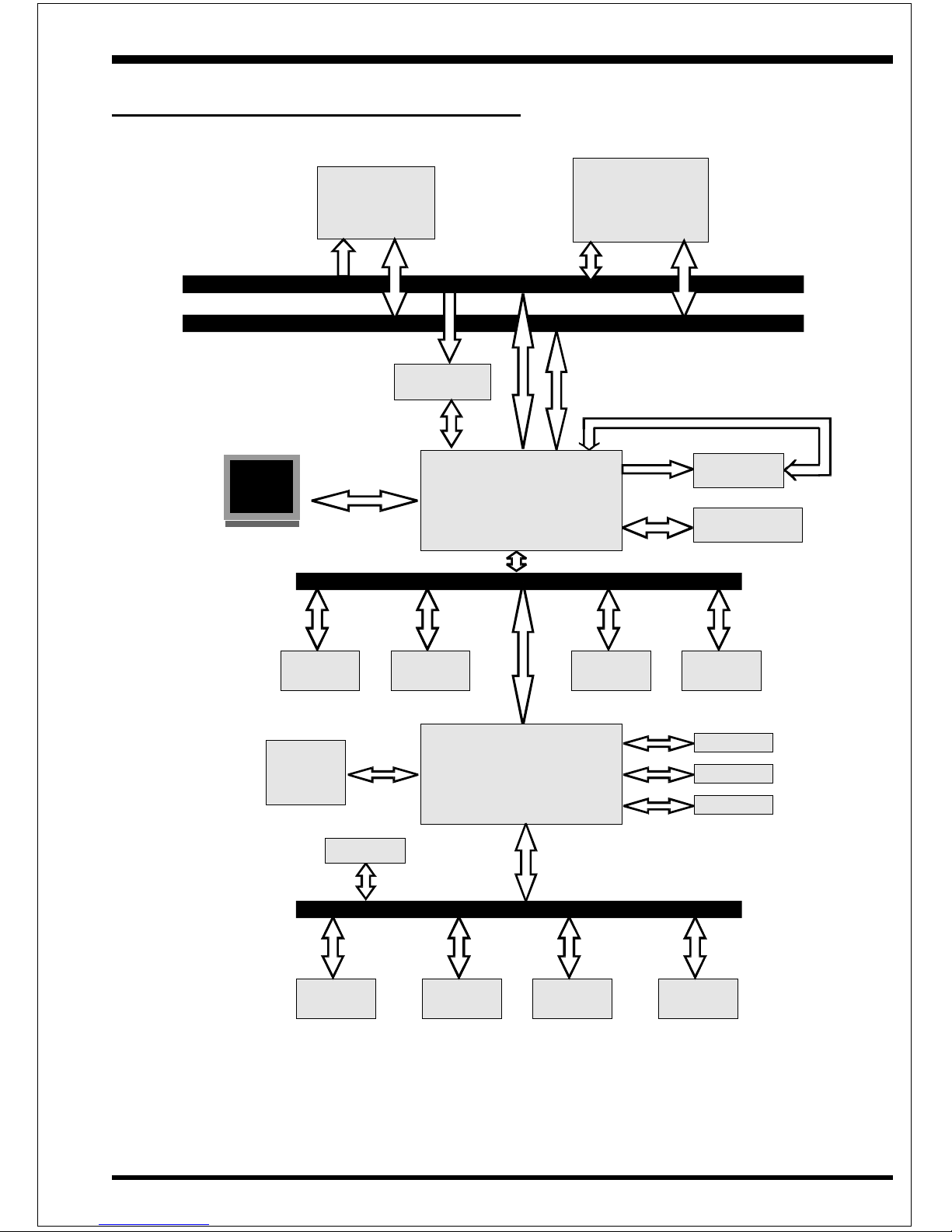
Figure 5: SiS530/SiS5595 System Block Diagram
System Block Diagram
CPU
PBSRAM
TAG RAM
SiS530
DRAM
IDE DEVICE
VGA Cable
PCI Bus
SIS5595
PCI
Device
PCI
Device
PCI
Device
PCI
Device
PCI
Device
PCI
Device
PCI
Device
PCI
Device
USB
GPIOs
Keyboard
H/W
Monitor
Sensors
ISA Bus
PCI
Device
ISA
Device
PCI
Device
ISA
Device
PCI
Device
ISA
Device
PCI
Device
ISA
Device
BIOS
Host Data Bus
Host Address Bus
MA Bus
IDE Bus
CRT Monitor
Page 8

Introduction S7-530A
Page 1-4
Page Left Blank
Page 9

FeaturesS7-530A
Page 2-1
Section 2
FEATURES
S7-530A Features:
• Intel Pentium
®
Processor, Pentium Processor with MMX technology, AMD
K5/K6, Cyrix 6x86L/6x86MX & idt C6 operating at 133 ~ 500 MHz with
321 ZIF socket 7 provides scalability to accept faster Processors in the
future.
• Designed with SiS530 Chipset.
• Supports up to 512 Mega of DRAM (minimum of 16 MB) on board, You can
use 168-pin DIMM x 2. It will automatically detect Extended Data Output
(EDO) DRAM at 66MHz only or Synchronous DRAM memory (SDRAM) at
66MHz or 100MHz (please see Section 3-4).
• Supports (2) 16 bit ISA slots, (2) 32 bit PCI slots, (2) independent high perfor
mance PCI IDE interfaces capable of supporting PIO Mode 3/4 and Ultra
DMA 66 devices. The S7-530A supports (2) PCI Bus Master slots and a
jumperless PCI INT# control scheme which reduces configuration confusion
when plugging in PCI card(s).
• Supports ATAPI (e.g. CD-ROM) devices on both Primary and Secondary IDE
interfaces.
• Designed with Winbond W83877TF Multi I/O: (1) floppy port, (1) parallel port
(EPP, ECP), and (2) serial ports (16550 Fast UART).
Note: Japanese “Floppy 3 mode” is also supported
• Built-in ATX 20-pin and supply connector.
• Features Award Plug & Play BIOS. With Flash Memory you can always
upgrade to the current BIOS as they are released.
• S7-530A utilizes a Lithium battery which provides environmental protection
and longer battery life.
• Software power-down when using Windows
®
95/98.
Page 10

Features S7-530A
Page 2-2
• Supports ring-in feature (remote power-on through external modem,
allows system to be turned on remotely.
• Resume by Alarm - Allows your system to turn on at a preselected time.
• Supports Keyboard power ON function (KBPO).
• Built-in WOL (W ake On Lan) Connector .
• Built-in ForteMedia FM801 PCI Sound.
• Built-in AGP 3D-Graphics.
Page 11
InstallationS7-530A
Page 3-1
Section 3
INSTALLATION
Page 12
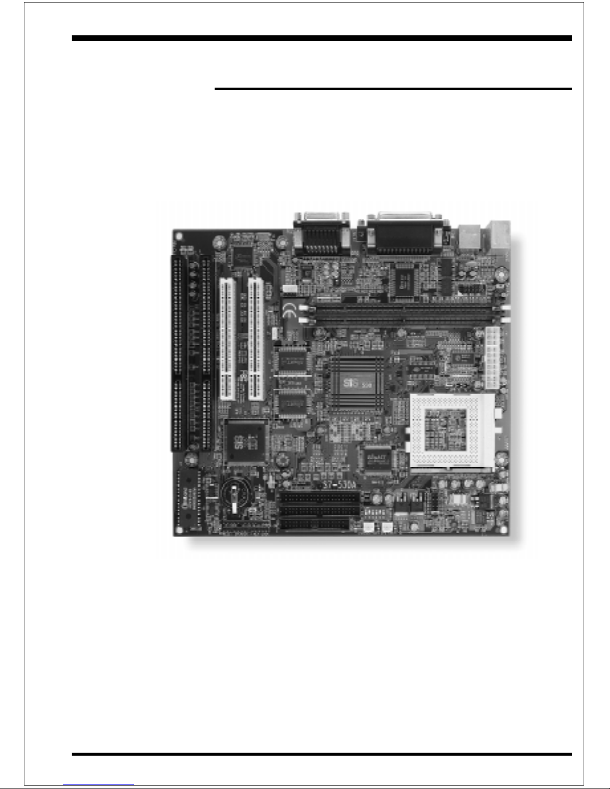
Installation S7-530A
Page 3-2
Figure 1
S7-530A Detailed Layout
64K*64
Battery
SIS530
PCIset
Winbond
83877
I/Oset
DIMM 1
DIMM 2
Bank 0
Bank 1
Flash Memory
for BIOS
J4
PCI Slot #1
PCI Slot #2
ISA Slot #2
SIS
5595
PCIset
J7:WOL
FDD1
IDE2
Secondary IDE
IDE1
J6
ISA Slot #1
J2
RESET
SPK
KEYLOCK
POWER_ON
1
J3
IR CONN.
+
+
SGRAM
SGRAM
CD2 CD1
1
JP4
1
JP1
1
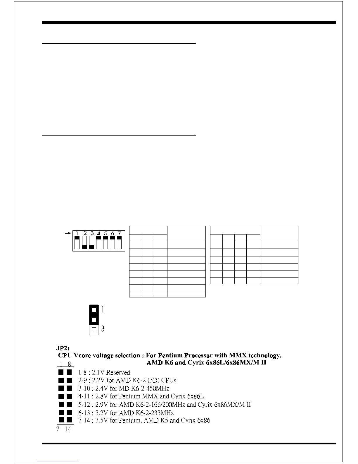
JP2
1
JP2
1
3.5V
3.2V
2.9V
2.8V
2.4V
2.2V
2.1V
CPU FAN
567
1
2
34
SW1
Chassis FAN
Page 13
InstallationS7-530A
Page 3-3
Easy Installation Procedure
The following must be completed before powering on your new system:
3-1. Configure DIP Switch and Jumper to match your hardware
3-2. Install memory chips
3-3. Device Connectors
Section 3-1
Configure DIP Switch
We design this motherboard with a DIP Switch to make your installation fast and
easy.
The following will describe all of the DIP Switch that you are required to set before
moving on to step 3-2.
Note: The DIP Switch as depicted as shown (Figure 1) in their correct
physical orientation.
S W1
1
2
3
ON
ON
2.0X
2.5X
3.0X
ON
CPU
Multi
p
lier
ON
ON
ON ON
3.5X
4.0X
4.5X
5.0X
5.5X
ON
ON
ON
ON
ON
ON
S W1
4
5
6
ON
ON
66MHz
75MHz
83MHz
CPU
BUS CLOCK
ON
ON
ON
90M Hz
95M Hz
ON
ON
ON ON
ON
7
ON
ON
ON
100MHz
JP1 C lear CO M S
1-2 : Run M ode(default)
2-3 : C lear C MO S
Page 14
Installation S7-530A
Page 3-4
* SDRAM only supports 8, 16, 32, 64, 128, 256MB DIMM modules.
Table 1
Section 3-2
System Memory Configuration
Memory Layout
The S7-530A supports (2) 168-pin DIMMs (Dual In-line Memory Module). The
DIMMs can be either EDO (Enhanced Data Out) or SDRAM (Synchronized
DRAM).
• DIMM SDRAM may be 83MHz (12ns), 100MHz (10ns) or
125MHz (8ns) bus speed.
• If you use both 50ns and 60ns memory you must configure
your BIOS to read 60ns.
• When using Synchronous DRAM we recommend using the
4 clock variety over the 2 clock.
Figure 2 and Table 1 show several possible memory configurations usingDIMM.
DIMM 1
DIMM 2
Bank 0
Bank 1
-Synchronous
-EDO
N ote : If you are installing just one D IMM , yo u m ust install it in D IM M 1
yromeMlatoT
1MMID
)0knaB(
2MMID
)1knaB(
BM652=
mumixaM
*MARDS/ODE
,BM46,BM23,BM61
1XBM652,BM821
enoN
BM215=
mumixaM
*MARDS/ODE
,BM46,BM23,BM61
1XBM652,BM821
*MARDS/ODE
,BM46,BM23,BM61
1XBM652,BM821
Figur e 2
Page 15
InstallationS7-530A
Page 3-5
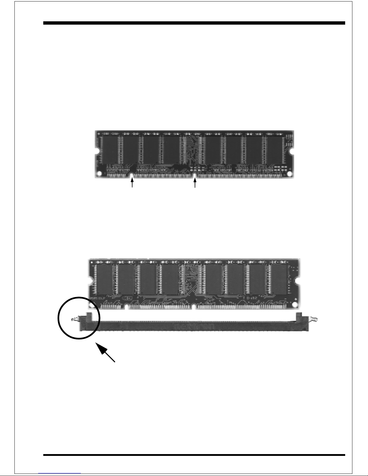
DIMM Module Installation
Figure 3 displays the notch marks and what they should look like on your DIMM
memory module.
DIMMs have 168-pins and two notches that will match with the onboard DIMM
socket. DIMM modules are installed by placing the chip firmly into the socket at a
90 degree angle and pressing straight down (figure 4) until it fits tightly into the DIMM
socket (figure 5).
Figure 3
CENTER KEY ZONE
(3.3 V DRAM)
LEFT KEY ZONE
(UNBUFFERED)
Figure 4
DIMM Module clip before installation
Page 16
Installation S7-530A
Page 3-6
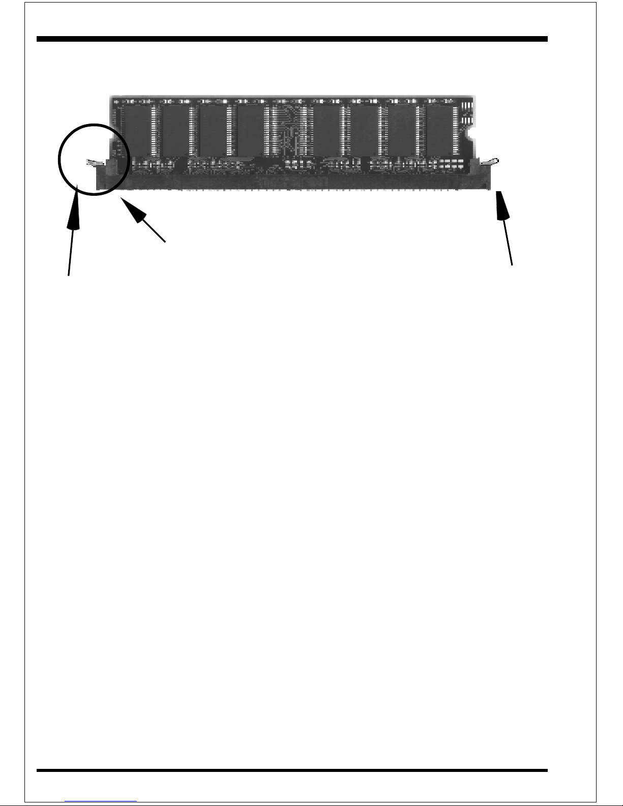
Figure 5
DIMM Module clip after installation
To remove the DIMM module simply press down both of the white clips on either side
and the module will be released from the socket.
Page 17

InstallationS7-530A
Page 3-7
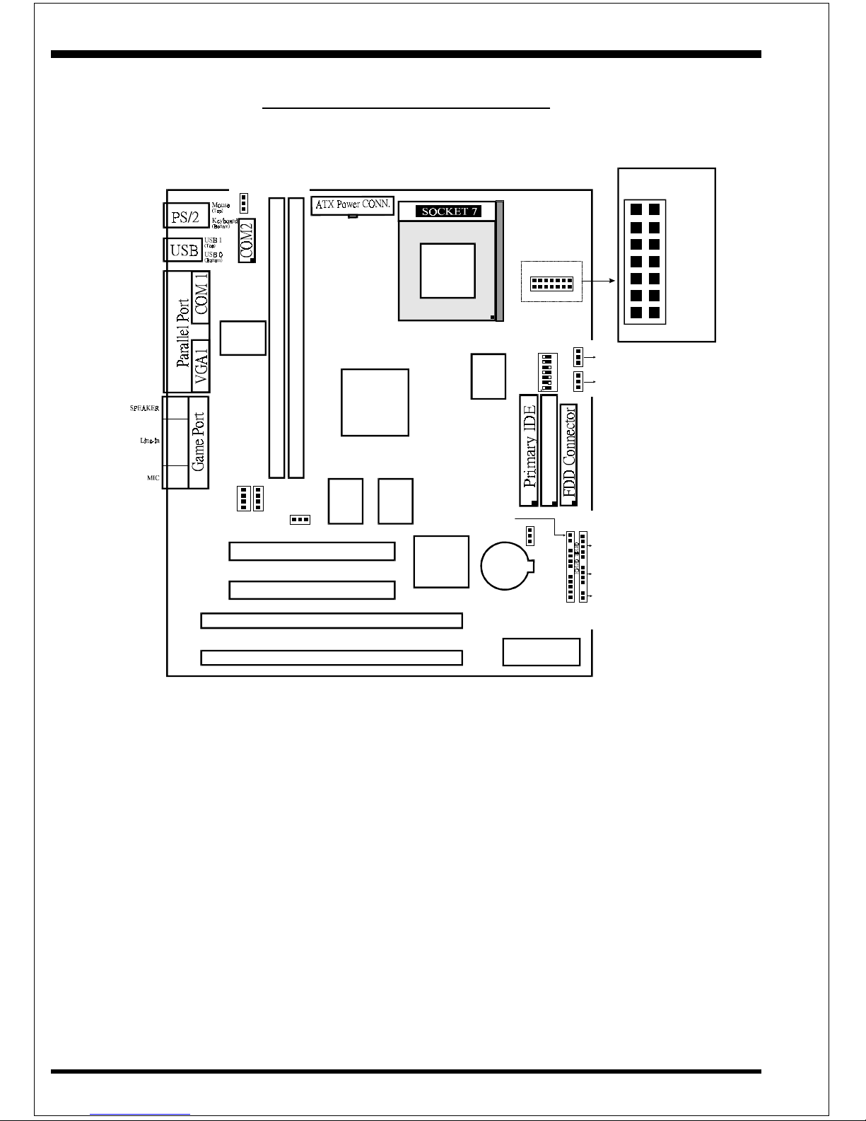
Section 3-3
Device Connectors
Please install the motherboard into the chassis.
Now that your motherboard is installed you are ready to connect all your connections
(figure 6).
J2: Chassis Panel Connector
• Keylock, Speaker, Reset
J3: Turbo LED, HDD LED, IR Conn., Sleep/Power_ON
J4: CPU Fan Power
• A plug-in for the CPU Fan Power
J6: Chassis Fan Power
• A plug-in for the chassis Fan Power
J7: WOL Connector
IDE1: Primary IDE
IDE2: Secondary IDE
FDD1:Floppy Controller Connector
PW1: ATX Power Connector
• 20-pin power connector
Figure 6
parallel port
MIC
Joystick/Midi port
USB port
COM1
VGA1
Speaker
Line_in
PS/2 Mouse
PS/2
KEYBOARD
Page 18

Installation S7-530A
Page 3-8
Power On/Off - This is connected to the power button on the case.
Using the Soft-Off by Pwr-BTTN feature, you can choose either
Instant Off (turns system off immediatly), or 4 sec delay (you need to
hold the button down for 4 seconds before the system turns off). When
the system is in 4 sec delay mode, we has added a special feature to
make the system go into suspend mode when the button is pressed
momentarily.
J2
Section3-4
Device Connectors (continued)
Speaker - Connect to the system's speaker for beeping
1. Speaker 3. GND
2. N/C 4. GND
Reset - Closed to restart system.
Turbo LED indicator - LED ON when higher speed is selected
IR Connector
1. VCC 4. GND
2. NC 5. IRTX
3. IRRX
IDE LED indicator - LED ON when Onboard PCI IDE Hard disks is
activate
KeyLock - Keyboard lock switch & Power LED connector
1. Power LED(+) 4. Keylock
2. N/C 5. GND
3. GND
J3
1
+
+
1
1
Page 19

BIOSS7-530A
Page 4-1
Section 4
AWARD BIOS SETUP
BIOS Instructions
Award’s ROM BIOS provides a built-in Setup program which allows user to modify
the basic system configuration and hardware parameters. The modified data will be
stored in a battery-backed CMOS, so that data will be retained even when the power
is turned off. In general, the information saved in the CMOS RAM will stay unchanged unless there is a configuration change in the system, such as hard drive
replacement or a device is added.
It is possible for the CMOS battery to fail, this will cause data loss in the CMOS
only. If this does happen you will need to reconfigure your BIOS settings.
To enter the Setup Program :
Power on the computer and press the <Del> key immediately, this will bring you into
the BIOS CMOS SETUP UTILITY.
Figure 1: CMOS Setup Utility
STANDARD CMOS SETUP SUPERVISOR PASSWORD
BIOS FEATURES SETUP USER PASSWORD
CHIPSET FEATURES SETUP IDE HDD AUTO DETECTION
POWER MANAGEMENT SETUP SAVE & EXIT SETUP
PNP/PCI CONFIGURATION EXIT WITHOUT SAVING
INTEGRATED PERIPHERALS
LOAD SETUP DEFAULTS
ROM PCI / ISA BIOS (2A5IMPA9)
CMOS SETUP UTILITY
AWARD SOFTWARE, INC.
ESC : QUIT : SELECT ITEM
F10 : Save & Exit Setup (Shift)F2 : Change Color
Time, Date, Hard Disk Type...
éé
éé
é
êê
êê
ê
èè
èè
è
çç
çç
ç
Page 20

BIOS S7-530A
Page 4-2
The menu displays all the major selection items. Select the item you need to
reconfigure. The selection is made by moving the cursor (press any direction key ) to
the item and pressing the ‘Enter’ key. An on-line help message is displayed at the
bottom of the screen as the cursor is moved to various items which provides a better
understanding of each function. When a selection is made, the menu of the selected
item will appear so that the user can modify associated configuration parameters.
4-1 Standard CMOS Setup
Choose “Standard CMOS Setup” in the CMOS SETUP UTILITY Menu (Figure 2).
The Standard CMOS Setup allows the user to configure system settings such as the
current date and time, type of hard disk drive installed, floppy drive type, and display
type. Memory size is auto-detected by the BIOS and displayed for your reference.
When a field is highlighted (use direction keys to move the cursor and the <Enter>
key to select), the entries in the field can be changed by pressing the <PgDn> or the
<PgUp> key.
Figure 2: Standard CMOS Setup
NOTE: If the hard disk Primary Master/Slave and Secondary Master/Slave
are set to Auto, then the hard disk size and model will be auto-detected.
ROM PCI/ISA BIOS(2A5IMPA9)
STANDARD CMOS SETUP
AWARD SOFTWARE, INC.
ESC : Quit : Select Item PU/PD/+/- : Modify
F1 : Help (Shift) F2 : Change Color
Date (mm:dd:yy) : Wed, Apr 17 1996
Time (hh:mm:ss) : 14 : 30 : 50
HARD DISKS TYPE SIZE CYLS HEAD PRECOMP LANDZONE SECTORS MODE
Primary Master : Auto 0 0 0 0 0 0 Auto
Primary Slave : Auto 0 0 0 0 0 0 Auto
Secondary Master : Auto 0 0 0 0 0 0 Auto
Secondary Slave : Auto 0 0 0 0 0 0 Auto
Drive A : 1.44M, 3.5 in.
Drive B : None
Floppy 3 Mode Support : Disabled
Video : EGA/VGA
Halt On : A11, But Keyboard
Base Memory : 640K
Extended Memory : 261120K
Other Memory : 384K
Total Memory : 262144K
éé
éé
é
êê
êê
ê
èè
èè
è
çç
çç
ç
Page 21

BIOSS7-530A
Page 4-3
NOTE: The “Halt On:” field is used to determine when to halt the system
by the BIOS if an error occurs.
NOTE: Floppy 3 Mode support is a mode used to support a special 3.5”
drive used in Japan. This is a 3.5” disk that stores only 1.2 MB, the default
setting for this is disabled.
4-2 BIOS Features Setup
Selecting the “BIOS FEATURES SETUP” option in the CMOS SETUP UTILITY
menu allows users to change system related parameters in the displayed menu. This
menu shows all of the manufacturer’s default values for the EP-61BXC-A.
Pressing the [F1] key will display a help message for the selected item.
Figure 3: BIOS Features Setup
Virus Warning: During and after the system boots up, any attempt to write to the
boot sector or partition table of the hard disk drive will halt the system and an error
message will appear.
You should then run an anti-virus program to locate the virus. Keep in mind that this
feature protects only the boot sector, not the entire hard drive.
The default value is Disabled.
ROM PCI/ISA BIOS(2A5IMPA9)
BIOS FEATURES SETUP
AWARD SOFTWARE, INC.
Virus Warning : Disabled Video BIOS Shadow : Enabled
CPU Internal Cache : Enabled C8000-CBFFF Shadow : Disabled
External Cache : Enabled CC000-CFFFF Shadow : Disabled
Quick Power On Self Test : Enabled D0000-D3FFF Shadow : Disabled
Boot Sequence : A, C, SCSI D4000-D7FFF Shadow : Disabled
Swap Floppy Drive : Disabled D8000-DBFFF Shadow : Disabled
Boot Up Floppy Seek : Enabled DC000-DFFFF Shadow : Disabled
Boot Up NumLock Status : On
Memory Parity Check : Disabled
Typematic Rate Setting : Disabled
Typematic Rate (Chars/Sec) : 6
Type matic Delay (Msec) : 250
Security Option : Setup
PCI/VGA Palette Snoop : Disabled
Assign IRQ For VGA : Enabled
OS Select For DRAM > 64MB : Non-OS2
Report No FDD For WIN 95 : Yes
Esc : Quit : Select Item
F1 : Help PU/PD/+/- : Modify
F5 : Old Values (Shift) F2 : Color
F7 : Load Setup Defaults
éé
éé
é
êê
êê
ê
èè
èè
è
çç
çç
ç
Page 22

BIOS S7-530A
Page 4-4
Enabled: Activates automatically when the system boots up causing a
warning message to appear when anything attempts to access the boot
sector.
Disabled: No warning message will appear when anything attempts to
access the boot sector.
Note: Many disk diagnostic programs that access the boot sector table can
trigger the virus warning message. If you plan to run such a program, we
recommend that you first disable the virus warning.
CPU Internal Cache: This controls the status of the processor’s internal cache
area.
The default is Enabled.
Enabled: This activates the processor’s internal cache thereby increasing
performance.
Disabled: This deactivates the processor’s internal cache thereby lowering
performance.
External (L2) Cache: This controls the status of the external (L2) cache area.
The default is Enabled.
Enabled: This activates the motherboard’s L2 cache thereby increasing
performance.
Disabled: This deactivates the motherboard’s L2 cache thereby lowering
performance.
Quick Power On Self Test: This category speeds up the Power On Self Test
(POST).
The default is Enabled.
Enabled: This setting will shorten or skip of the items checked during
POST.
Disabled: Normal POST.
Boot Sequence: This category determines which drive is searched first by the O/S
(Operating System).
The default is A,C,SCSI.
The following is your list of options:
[A, C, SCSI] - [C, A, SCSI] - [C, CD-ROM, A] - [CD-ROM, C, A]
[D, A,CD-ROM],[E, A, CD-ROM] - [F, A, CD-ROM] - [SCSI, A, C]
[SCSI C, A] - [C Only]
Page 23

BIOSS7-530A
Page 4-5
Swap Floppy Drive: This will swap your physical drive letters A & B if you are
using two floppy disks.
The default is Disabled.
Enabled: Floppy A & B will be swapped under the O/S.
Disabled: Floppy A & B will be not swapped.
Boot Up Floppy Seek: During Power-On-Self-Test (POST), BIOS will determine
if the floppy disk drive installed is 40 or 80 tracks. Only 360K type is 40 tracks while
760K, 1.2MB and 1.44MB are all 80 tracks.
The default is Enabled.
Enabled: The BIOS will search the floppy disk drive to determine if it is 40
or 80 tracks.
Disabled: The BIOS will not search for the type of floppy disk drive by
track number.
NOTE: BIOS can not tell the difference between 720K, 1.2MB and 1.
44MB drive types as they are all 80 tracks.
Boot Up NumLock Status: This controls the state of the NumLock key when the
system boots.
The default is On.
On: The keypad acts as a 10-key pad.
Off: The keypad acts like the cursor keys.
Typematic Rate Setting: This determines the keystrokes repeat rate.
The default is Disabled.
Enabled: Allows typematic rate and typematic delay programming.
Disabled: The typematic rate and typematic delay will be controlled by the
keyboard controller in your system.
Typematic Rate (Chars/Sec): This is the number of characters that will be repeated by a keyboard press.
The default is 6.
6: 6 characters per second. 8: 8 characters per second.
10: 10 characters per second. 12: 12 characters per second.
15: 15 characters per second. 20: 20 characters per second.
24: 24 characters per second. 30: 30 characters per second.
Page 24

BIOS S7-530A
Page 4-6
Typematic Delay (msec): This setting controls the time between the first and the
second character displayed by typematic auto-repeat.
The default is 250.
250: 250 msec.
500: 500 msec.
750: 750 msec.
1000: 1000 msec.
Security Option: This category allows you to limit access to the System and Setup,
or just to Setup.
The default is Setup.
System: The system will not boot and the access to Setup will be denied if
the correct password is not entered at the prompt.
Setup: The system will boot; but the access to Setup will be denied if the
incorrect password is not entered at the prompt.
PCI/VGA Palette Snoop: This field controls the ability of a primary PCI VGA
controller to share a common palette (When a snoop write cycles) with an ISA video
card.
The default is Disabled.
Enabled: If an ISA card is connected to a PCI VGA card via the VESA
connector, and that ISA card connects to a VGA monitor, then that ISA card
uses the RAMDAC of the PCI card.
Disabled: Disables the VGA card Palette Snoop function.
Assign IRQ For VGA: This option allows BIOS to assign IRQ for VGA device
Enabled: The system was assigned IRQ for VGA Card.
Disabled: The system was not assigned IRQ for VGA Card.
OS Select For DRAM > 64MB: Some operating systems require special handling.
Use this option only if your system has greater than 64MB of memory.
The default is Non-OS2.
OS2: Select this if you are running the OS/2 operating system with greater
than 64MB of RAM.
Non-OS2: Select this for all other operating systems and configurations.
Report No FDD For WIN95: This option allows BIOS to indicate whether
WIN95 is with FDD or not. The Default value is NO.
NO: Report No FDD for WIN95.
Page 25

BIOSS7-530A
Page 4-7
YES: Report FDD for WIN95
Video BIOS Shadow: This option allows video BIOS to be copied into RAM.
Video Shadowing will increase the video performance of your system.
The default is Enabled.
Enabled: Video shadow is enabled.
Disabled: Video shadow is disabled.
C8000 - CBFFF Shadow:
CC000 - CFFFF Shadow:
D0000 - D3FFF Shadow:
D4000 - D7FFF Shadow:
D8000 - DBFFF Shadow:
DC000 - DFFFF Shadow:
These categories determine whether ROMs from option cards will be copied into
RAM. This will be in 16K byte or 32K byte units, and the size will depend on chipset
of the option card.
Enabled: Optional shadow is enabled.
Disabled: Optional shadow is disabled.
Page 26

BIOS S7-530A
Page 4-8
4-3 Chipset Features Setup
Choose the “CHIPSET FEATURES SETUP” in the CMOS SETUP UTILITY
menu to display following menu.
Figure 4: Chipset Features Setup
Refresh Rate Control: Select the period required to refresh the DRAMs, according to DRAM specifications.
The default is 15.6us.
The choice: 3.9us, 7.8us, 15.6us:
Ref/Act Command Delay: Set the DRAM clock of the refresh command to
refresh/active command delay.
The default is 6T.
The choice: 5T, 6T, 7T, 8T:
Refresh Queue Depth: Set the depth of refresh queue.
The default is 12.
The choice: 0, 4, 8, 12
ROM PCI/ISA BIOS(2A5IMPA9)
CHIPSET FEATURES SETUP
AWARD SOFTWARE, INC.
Refresh Rate Control : 15.6us System BIOS Cacheable : Disabled
Ref/Act Command Delay : 6T Video BIOS Cacheable : Enabled
Refresh Queue Depth : 12 Memory Hole at 15M-16M : Disabled
RAS Precharge Time : 3T PCI Post Write Buffer : Disabled
RAS to CAS Delay : 3T PCIDelayed Transaction : Disabled
ISA Bus Clock Frequency : PCICLK/4 Auto Detect DIMM/PCI Clk : Enabled
Starting Point of Paging : 1T Spread Spectrum : Disabled
NA# Enabled : Enabled
L2 Cache Burst RD Cycle : Delay 1 T
SDRAM CAS Latency : 3T
SDRAM WR Retire Rate : x-1-1-1
DRAM opt RAM Precharge : Enabled
PCI Peer Concurrency : Enabled
Read Prefetch Memory RD : Enabled
Assert TRDY After Prefet : 2 QWs
CPU to PCI Burst Mem. WR : Enabled
CPU to PCI Post Write : Enabled
AGP Aperture Size : 64MB
Esc : Quit : Select Item
F1 : Help PU/PD/+/- : Modify
F5 : Old Values (Shift) F2 : Color
F7 : Load Setup Defaults
éé
éé
é
êê
êê
ê
èè
èè
è
çç
çç
ç
Page 27

BIOSS7-530A
Page 4-9
Ras Precharge Time: The precharge time is the number of cycles it takes for the
RAS to accumulate its charge before DRAM refreshes. If insufficient time is
allowed, refresh may be incomplete and the DRAM may fail to retain data.
The default is 3T
The choice: 2T, 3T, 4T, 5T
RAS to CAS Delay: When DRAM is refreshed, both rows and columns are
addressed separately. This setup item allows you to determine the timing of the
transition from RAS(row address strobe) to CAS(column address strobe).
The default is 3T.
The choice: 2T, 3T, 4T, 5T
ISA Bus Clock Frequency: You can set the speed of the AT bus at one-third or
one-fourth of the CPU clock speed.
The default is PCICLK/4.
The choice: 7.159MHz, PCICLK/3, PCICLK/4
Starting Point of Paging: This value controls the start timing of memory paging
operations.
The default is 1T.
The choice: 1T, 2T, 4T,8T
NA# Enable: Selecting Enabled permits pipelining, in which the chipset signals the
CPU for a new memory address before all data transfers for the current cycle are
complete, resulting in faster performance.
The default is Enabled.
L2 Cache Burst RD Cycle: These timing numbers are the pattern of cycles the
CPU uses to read data from the cache.
The default is Delay 1T
The choice: Normal, Delay 1T
SDRAM CAS Latency: When synchronous DRAM is installed, the number of
clock cycles of CAS latency depends on the DRAM timing. Do not reset this field
from the default value specified by the system designer.
The default is 3T.
The choice: 2T, 3T
Page 28

BIOS S7-530A
Page 4-10
SDRAM WR Retire Rate: The system designer must select the correct timing for
data transfers from the write buffer to memory, according to DRAM specifications.
The default is X-1-1-1.
The choice: 0WS, 1WS
DRAM Opt RAS Precharge: The precharge time is the number of cycles it takes
for the RAS to accumulate its charge before DRAM refreshes. If insufficient time
is allowed, refresh may be incomplete and the DRAM may fail to retain data.
The default is Enabled.
The choice: Enabled, Disabled
PCI Peer Concurrency: Peer concurrency means that more than one PCI device
can be active at a time.
The default is Enabled.
The choice: Enabled, Disabled:
Read Prefetch Memory RD: When this item is Enabled, the system is allowed to
prefetch the next read instruction and initiate the next process.
The default is Enabled.
Assert TRDY After Prefet: When you select 1QWs SiS530 asserts its first
TRDY# for 1 transaction after it prefetched 1 quadword of data from system
memory. Otherwise, SiS530 asserts its first TRDY# after 2 quadwords are
prefetched.
The default is 2 QWs.
CPU to PCI Burst Mem. WR: Select Enabled permits PCI burst memory write
cycles, for faster performance. When Disabled, performance is slightly slower, but
more reliable.
The default is Enabled.
CPU to Post Write: Select Enabled to use a fast buffer for posting writes to
memory. Using a fast buffer releases the CPU before completion of a write cycle to
DRAM.
The default is Enabled.
Page 29

BIOSS7-530A
Page 4-11
AGP Aperture Size: The amount of system memory that the AGP card is allowed
to share.
The default is 64.
4: 4MB of systems memory accessable by the AGP card.
8: 8MB of systems memory accessable by the AGP card.
16: 16MB of systems memory accessable by the AGP card.
32: 32MB of systems memory accessable by the AGP card.
64: 64MB of systems memory accessable by the AGP card.
128: 128MB of systems memory accessable by the AGP card.
256: 256MB of systems memory accessable by the AGP card.
System BIOS Cacheable: This allows you to copy your BIOS code from slow
ROM to fast RAM.
The default is Enabled.
Enabled: The option will improve system performance. However, if any
program writes to this memory area, a system error may result.
Disabled: System BIOS non-cacheable.
Video BIOS Cacheable: This option copies the video ROM BIOS to fast RAM
(C0000h to C7FFFh).
The default is Enabled.
Enabled: Enables the Video BIOS Cacheable to speed up the VGA
Performance.
Disabled: Will not use the Video BIOS Cacheable function.
Memory Hole at 15M-16M: You can reserve this memory area for the use of
ISA adaptor ROMs.
The default is Disabled.
Enabled: This field enables the main memory (15~16MB) to remap to ISA
BUS.
Disabled: Normal Setting.
NOTE: If this feature is enabled you will not be able to cache this
memory segment.
Page 30

BIOS S7-530A
Page 4-12
Auto Detect DIMM/PCI Clk: Allows you to stop DIMM/PCI Clock drive when
the DIMM site or PCI Slot are not plug. This item may help reduce EMI.
The default is Enabled.
Enabled: Provides unused DIMM/PCI to stop.
Disabled: Provides the clock generator always driving.
Spread Spectrum : Allows you to active the Spread Spectrum function for reduce
EMI. (Note: When Enabled the item that performance will be impacted).
The default is Disabled.
Enabled: Provides the Spread Spectrum function from clock generator.
Disabled: NO Spread Spectrum function.
4-4 Power Management Setup
Choose the “POWER MANAGEMENT SETUP” in the CMOS SETUP UTILITY
to display the following screen. This menu allows the user to modify the power
management parameters and IRQ signals. In general, these parameters should not be
changed unless it’s absolutely necessary.
Figure 5: Power Management Setup
You can only change the content of Doze Mode, Standby Mode, and Suspend Mode
when the Power Management is set to ‘User Define’.
ROM PCI/ISA BIOS (2A5IMPA9)
POWER MANAGEMENT SETUP
AWARD SOFTWARE, INC.
ACPI Function : Enabled VGA Activity : Enabled
Power Management : User Define IRQ [3-7, 9-15], NMI : Enabled
Video off option : Susp, Stby -> off IRQ 8 Break Suspend : Disabled
Video off Method : V/H SYNC+Blank Power Button Over Ride : Delay 4 Sec
Switch Function : Break/Wake Ring Power Up Control : Enabled
Doze Speed (div by) : 2/ 8 GPIO5 Power Up Control : Enabled
Stdby Speed (div by) : 1/8 KB Power ON Password : Enter
MODEM Use IRQ : 9 Power Up by Alarm : Disabled
Hot Key Function As : Power off
** PM Timers **
HDD off After : Disabled
Doze Mode : Disabled
Standby Mode : Disabled
Suspend Mode : Disbaled
** PM Events **
HDD Ports Activity : Enabled
COM Ports Activity : Enabled
LPT Ports Activity : Enabled
Esc : Quit : Select Item
F1 : Help PU/PD/+/- : Modify
F5 : Old Values (Shift) F2 : Color
F7 : Load Setup Defaults
éé
éé
é
êê
êê
ê
èè
èè
è
çç
çç
ç
Page 31

BIOSS7-530A
Page 4-13
ACPI Function: This option allows you to select ACPI Function.
The default is Enabled.
Enabled: Support ACPI function for new O.S
Disabled: No Support ACPI function.
Power Management: Use this to select your Power Management selection.
The default is User define.
Disabled: The system operates in NORMAL conditions (Non-GREEN), and
the Power Management function is disabled.
Max. saving: Maximum power savings. Inactivity period is 1 minute in each
mode.
Min. saving: Minimum power savings. Inactivity period is 1 hour in each
mode.
User define: Allows user to define PM Timers parameters to control power
saving mode.
Video off Option: When enabled, this feature allows the VGA adapter to operate
in a power saving mode.
The default is susp, stby -> off
Always On: Monitor will remain on during power saving modes.
Suspend-->Off: Monitor blanked when the systems enters the Suspedn
mode.
Susp, Stby -> Off: Monitor blanked when the system enters either Suspend
or Standby modes.
Susp, Stby -> Off: Monitor blanked when the system enters any power
saving mode.
Video Off Method: This option allows you to select how the video will be disabled
by the power management.
The default is V/H Sync + Blank
V/H Sync + Blank: System turns off vertical and horizontal synchronization
ports and writes blanks to the video buffer.
DPMS: Select this option if your monitor supports the Display Power
Management Signaling (DPMS) standard of the Video Electronics Standards Association (VESA). Use the software supplied for your video subsystem to select video power management values.
Blank Screen: System only writes blanks to the video buffer.
Page 32

BIOS S7-530A
Page 4-14
Switch Function: You can choose whether or not to permit your system to enter
complete Suspend mode. Suspend mode offers greater power savings, wiht a
correspondingly longer awakening period.
The default is Break/wake.
Doze Speed (div by): Sets the CPU’s speed during Doze mode. The speed is
reduced to a fraction of the CPU’s normal speed. The divisors range from 1 to 8.
Stdby Speed (div by): Select a divisor to reduce the CPU speed during Standby
mode to a fraction of the full CPU speed. The speed is reduced to a fraction of the
CPU’s normal speed. The divisors range from 1 to 8.
MODEM Use IRQ: Name the interrupt request (IRQ) line assigned to the modem
(if any) on your system. Activity of the selected IRQ always awakens the system.
Default is IRQ 9.
N/A: No IRQ is used. 3 : IRQ 3
4: IRQ 4 5: IRQ 5
7: IRQ 7 9: IRQ 9
10: IRQ 10 11: IRQ 11
The S7-530A supports HDD Power Down, Doze and Standby power saving functions when using the Intel Pentium II Processor.
The default is Disabled
Hot Key Power Off: Select Enabled if your system has a hot key for soft power
off.
PM Timers
The following four modes are Green PC power saving functions which are
only user configurable when User Defined power management has been selected.
See above for available selections.
HDD Off After: By default, this item is Disabled, meaning that no matter the mode
the rest of the system, the hard drive will remain ready. Otherwise, you have a
range of choices from 1 to 15 minutes or Suspend. This means that you can elect to
have your hard disk drive be turned off after a selected number of minutes or when
the rest of the system goes into a Suspend mode.
Page 33

BIOSS7-530A
Page 4-15
Doze Mode: When enabled and after the set time of system inactivity, the
CPUclock will run at slower speed while all other devices still operate at full speed.
Standby Mode: When enabled and after the set time of system inactivity, the fixed
disk drive and the video would be shut off while all other devices still operate at full
speed.
Suspend Mode: When enabled and after the set time of system inactivity, all
devices except the CPU will be shut off.
PM Events
You may disabled activity monitoring of some common I/O events and interrupt
requests so they do not wake up the system. The default wake-up event is keyboard
activity.
When On(or named, in the case of LPT & COM), any activity from one of the listed
system peripheral devices or IRQs wakes up the system.
HDD Ports Activity: When set to On(default), any event occurring at a HDD
(serial) port will awaken a system which has been powered down.
COM Ports Activity: When set to On(default), any event occurring at a hard or
floppy drive port will awaken a system which has been powered down.
LPT Ports Activity: When set to On(default), any event occurring at a LPT
(printer) port will awaken a system which has been powered down.
VGA Activity: When set to On(default), any event occurring at VGA will awaken
a system which has been powered down.
The following is a list of IRQ’s, Interrupt ReQuests, which can be exempted much as
the COM ports and LPT ports above can. When an I/O device wants to gain the
attention of the operating system, it signals this by causing an IRQ to occur. When
the operating system is ready to respond to the request, it interrupts itself and performs the service.
As above, the choices are On and off.
When set On,activity will enither prevent the system from going into a power man-
agement mode nor awaken it.
l IRQ [3-7, 9-15], NMI
Page 34

BIOS S7-530A
Page 4-16
l IRQ 8 Break Suspend: You can Enabled or Disabled monitoring of IRQ8
(the Real Time Clock) so it does not awaken the system from Suspend mode.
Power Button Over Ride: You could press the power button for more than 4
seconds forces the system to enter the Soft-Off state when the system has “hung”.
Ring Power Up Control: When you select Enabled, a signal from ring returns the
system to Full On state.
GPIO5 Power Up Control: When you select Enabled, a signal from General
Purpose Input 05 returns the system to Full On state.
KB Power ON Password: When you set a password for keyboard. The password
you set the keyboard that returns the system to Full On state.
To install a password, follow these steps:
1.Highlight the item Password Settings on the main menu and press Enter.
2. The password dialog box will appear.
3. If you are installing a new password, carefully type in the password. You
cannot use more than 8 characters or numbers. The password will differenti
ate between upper case and lower characters. Press Enter after you have
typed in the password. If you are deleting a password that is already installed
just press Enter when the password dialog box appears.
4. The system will ask you to cnfirm the new password by asking you to type it
in a second time. Carefully type the password again and press Enter, or just
press Enter if ypu are deleting a password that is already installed.
5. If you typed the password correctly, the password will be installed.
Power Up by Alarm: When you select Enabled, the following fields appear. They
let you set the alarm that returns the system to Full On state.
Page 35

BIOSS7-530A
Page 4-17
4-5 PNP/PCI Configuration
The PNP/PCI configuration program is for the user to modify the PCI/ISA IRQ
signals when various PCI/ISA cards are inserted in the PCI or ISA slots.
WARNING: Conflicting IRQ’s may cause the system to not find certain devices.
Figure 6: PCI Configuration Setup
Resources Controlled By: Who controlled the system PNP/PCI resources.
The default is Manual.
Manual: PNP Card’s resources will be controlled manually. You can set
which IRQ-X and DMA-X are assigned to PCI/ISA PNP or Legacy ISA
Cards.
Auto: If your ISA card and PCI card are all PNP cards, BIOS will assign
the interrupt resource automatically.
Reset Configuration Data: This setting allows you to clear ESCD data.
The default is Disabled
Disabled: Normal Setting.
Enabled: If you have plugged in some Legacy cards to the system and they
were recorded into ESCD (Extended System Configuration Data), you can
set this field to Enabled in order to clear ESCD.
ROM PCI/ISA BIOS(2A5IMPA9)
PNP/PCI CONFIGURATION
AWARD SOFTWARE, INC.
Resources Controlled By : Auto PCI IRQ Actied By : Level
Reset Configuration Data : Disabled Assign IRQ FOR USB : Enabled
Slot 1 use IRQ No : Auto
Slot 2 use IRQ No : Auto
Slot 3 use IRQ No : Auto
PCI Audio use IRQ No : 9
Esc : Quit : Select Item
F1 : Help PU/PD/+/- : Modify
F5 : Old Values (Shift) F2 : Color
F7 : Load Setup Defaults
éé
éé
é
êê
êê
ê
èè
èè
è
çç
çç
ç
Page 36

BIOS S7-530A
Page 4-18
PCI IRQ Activated: This sets the method by which the PCI bus recognizes that an
IRQ service is being requested by a device. Under all circumstances, you should
retain the default configuration unless advised otherwise by your system’s
manufacturer.
Level:
Edge:
Assign IRQ For USB: This item allows BIOS to assign whether IRQ is with USB
or not. If you have not connect the USB device. Can release the IRQ for other
device.
The default is Enabled.
Enalbed: Provides IRQ for USB device.
Disabled: Release IRQ for other device.
4-6 Load Setup Defaults
The “LOAD SETUP DEFAULTS” function loads the system default data directly
from ROM and initializes the associated hardware properly. This function will be
necessary only when the system CMOS data is corrupted.
Page 37

BIOSS7-530A
Page 4-19
4-7 Integrated Peripherals
Figure 8: Integrated Peripherals
Note: If you do not use the Onboard IDE connector, then you will need to
set Onboard Primary PCI IDE: Disabled and Onboard Secondary PCI
IDE: Disabled
Note: The Onboard PCI IDE cable should be equal to or less than 18
inches (45 cm.).
IDE Primary Master PIO
The default is Auto.
Auto: BIOS will automatically detect the Onboard Primary Master PCI IDE
HDD Accessing mode.
Mode 0~4: Manually set the IDE Programmed interrupt mode.
IDE Primary Slave PIO
The default is Auto.
Auto: BIOS will automatically detect the Onboard Primary Slave PCI IDE
HDD Accessing mode.
Mode 0~4: Manually set the IDE Programmed interrupt mode.
ROM PCI/ISA BIOS(2A5IMPA9)
INTEGRATED PERIPHERALS
AWARD SOFTWARE, INC.
Internal PCI/IDE : Both Onboard Parallel Mode : ECP/EPP
IDE Primary Master PIW : Auto ECP Mode Use DMA : 3
IDE Primary Slave PIO : Auto Parallel Port EPP Type : EPP1.9
IDE Secondary Master PIO : Auto PS/2 mouse function : Enabled
IDE Secondary Slave PIO : Auto USB Keyboard Support : Disabled
Primary Master UltraDMA : Auto USB Keyboard Support : Disabled
Primary Slave UltraDMA : Auto Init Display First : PCI Slot
Secondary MasterUltraDMA : Auto
Secondary Slave UltraDMA : Auto
IDE Burst Mode : Enabled Current CPU Telmperature : 71oC/159oF
IDE Data Port Post Write : Disabled Current CPU Fan Speed : 4245 RPM
IDE HDD Block Mode : Enabled Current ChassisFan Speed : 0 RPM
+12V : 12.41V Vcc : 5.00V
Onboard FDD Controller : Enabled Vio : 3.45V Vcore : 2.90V
Onboard Serial Port 1 : 3F8/IRQ4
Onboard Serial Port 2 : 2F8/IRQ3
UART 2 Mode : Standard
Onboard Parallel Port : 378/IRQ7
Esc : Quit : Select Item
F1 : Help PU/PD/+/- : Modify
F5 : Old Values (Shift) F2 : Color
F7 : Load Setup Defaults
éé
éé
é
êê
êê
ê
èè
èè
è
çç
çç
ç
Page 38

BIOS S7-530A
Page 4-20
IDE Secondary Master PIO:
The default is Auto.
Auto: BIOS will automatically detect the Onboard Secondary Master PCI
IDE HDD Accessing mode.
Mode 0~4: Manually set the IDE Programmed interrupt mode.
IDE Secondary Slave PIO:
The default is Auto.
Auto: BIOS will automatically detect the Onboard Secondary Slave PCI IDE
HDD Accessing mode.
Mode 0~4: Manually set the IDE Programmed interrupt mode.
Primary Master UltraDMA: This allows you to select the mode of operation for
the hard drive.
The default is Auto.
Auto: The computer will select the optimal setting.
Disabled: The hard drive will run in normal mode.
Primary Slave UltraDMA: This allows you to select the mode of operation for the
hard drive.
The default is Auto.
Auto: The computer will select the optimal setting.
Disabled: The hard drive will run in normal mode.
Secondary MasterUltraDMA: This allows you to select the mode of operation for
the hard drive.
The default is Auto.
Auto: The computer will select the optimal setting.
Disabled: The hard drive will run in normal mode.
Secondary Slave UltraDMA: This allows you to select the mode of operation for
the hard drive.
The default is Auto.
Auto: The computer will select the optimal setting.
Disabled: The hard drive will run in normal mode.
IDE HDD Block Mode: IDE Block Mode allows the controller to access blocks
of sectors rather than a single sector at a time.
The default is Enabled.
Page 39

BIOSS7-530A
Page 4-21
Enabled: Enabled IDE HDD Block Mode. Provides higher HDD
transfer rates.
Disabled: Disable IDE HDD Block Mode.
Onboard FDD Controller: This controls the state of the onboard floppy controller.
The default value is Enabled.
Enabled: Enable the Onboard Winbond Chips’s floppy drive interface
controller.
Disabled: Disable the Onboard Winbond Chip’s floppy drive interface
controller.
Onboard Serial Port 1: This field allows the user to configure the 1st serial port.
The default is 3F8/IRQ4.
AUTO: Enable Onboard Serial port 1 and address is Auto adjusted
COM1: Enable Onboard Serial port 1 and address is 3F8H/IRQ4.
COM2: Enable Onboard Serial port 1 and address is 2F8H/IRQ3.
COM3: Enable Onboard Serial port 1 and address is 3E8H/IRQ4.
COM4: Enable Onboard Serial port 1 and address is 2E8H/IRQ3.
Disabled: Disable Onboard winboard CHIP’s Serial port 1.
Onboard Serial Port 2: This field allows the user to configure the 2nd serial port.
The default is 2F8/IRQ3.
AUTO: Enable Onboard Serial port 2 and address is Auto adjusted
COM1: Enable Onboard Serial port 2 and address is 3F8H/IRQ4.
COM2: Enable Onboard Serial port 2 and address is 2F8H/IRQ3.
COM3: Enable Onboard Serial port 2 and address is 3E8H/IRQ4.
COM4: Enable Onboard Serial port 2 and address is 2E8H/IRQ3.
Disabled: Disable Onboard winboard CHIP’s Serial port 2.
Onboard UART 2 Mode:The default value is standard. This field allows the User
to select the COM2 port that can support a serial Infrared Interface.
The default is Standard
Standard: Support a Serial Infrared Interface IrDA.
QHPSIR: Support a HP Serial Infrared Interface format.
ASKIR: Support a Sharp Serial Infrared Interface format.
Page 40

BIOS S7-530A
Page 4-22
Onboard Parallel port: This field allows the user to configure the LPT port.
The default is 378 / IRQ7.
378H: Enable Onboard LPT port and address is 378H and IRQ7.
278H: Enable Onboard LPT port and address is 278H and IRQ5.
3BCH: Enable Onboard LPT port and address is 3BCH and IRQ7.
Disabled: Disable Onboard Winbond Chip’s LPT port.
Parallel port Mode: This field allows the user to sellect the parallel port mode. The
default value is ECP+EPP.
Normal: Standard mode. IBM PC/AT Compatible bidirectional parallel
port.
EPP : Enhanced Parallel Port mode.
ECP : Extended Capability Port mode.
EPP+ECP: ECP Mode & EPP Mode.
ECP Mode USE DMA: This field allows the user to select DMA1 or DMA3 for
the ECP mode.
The default is 3.
1:This field selects the routing of DMA1 for the ECP mode.
3:This field selects the routing of DMA3 for the ECP mode.
USB Keyboard Support: This controls the activation status of an optional USB
keyboard that may be attached.
The default is disabled.
Enabled: Enable USB keyboard support.
Disabled: Disable USB keyboard support.
Current CPU Temperature: This is the current temperature of the CPU.
Current CPU FAN Speed: The current CPU fan speed in RPMs.
Current Chassis FAN Speed: The current chassis fan speed in RPMs.
Vcore: The voltage level of the CPU.
Vio: The voltage level of the M/B’s I/O.
Vio, +5V, +12V: The voltage level of the switch power supply.
Page 41

BIOSS7-530A
Page 4-23
4-8 Change Supervisor or
User Password
To change the password, choose the “SUPERVISOR PASSWORD or USER
PASSWORD” option from the CMOS SETUP UTILITY menu and press [Enter].
NOTE: Either “Setup” or “System” must be selected in the “Security
Option” of the BIOS FEATURES SETUP menu.
1. If CMOS is corrupted or the option was not used, a default password stored
in the ROM will be used. The screen will display the following message:
Enter Password:
Press the [Enter] key to continue after the proper password is given.
2. If the CMOS is corrupted or the option was used earlier and the user wishes
to change the default password, the SETUP UTILITY will display a message and ask for a confirmation.
Confirm Password:
3. After pressing the [Enter] key (ROM password if the option was not used)
or current password (user-defined password), the user can change the
Page 42

BIOS S7-530A
Page 4-24
password and store new one in CMOS RAM. A maximum of 8 characters
can be entered.
4-9 IDE HDD Auto Detection
The “IDE HDD auto detection” utility is a very useful tool, especially when you do
not know which kind of hard disk type you are using. You can use this utility to detect
the correct disk type installed in the system automatically. But now you can set
HARD DISK TYPE to Auto in the STANDARD CMOS SETUP. You don’t need
the “IDE HDD AUTO DETECTION” utility. The BIOS will Auto-detect the hard
disk size and model on display during POST.
Figure 8: IDE HDD Auto Detection
NOTE: HDD Modes
The Award BIOS supports 3 HDD modes : NORMAL, LBA & LARGE NORMAL
mode
Generic access mode in which neither the BIOS nor the IDE controller will make
any transformations during accessing.
The maximum number of cylinders, head & sectors for NORMAL mode are.
ROM PCI/ISA BIOS(2A5IMPA9)
CMOS SETUP UTILITY
AWARD SOFTWARE, INC.
HARD DISKS TYPE SIZE CYLS HEADS PRECOMP LANDZONE SECTORS MODE
Primary Master :
Select Secondary Slave Option (N=Skip) : N
OPTIONS SIZE CYLS HEAD PRECOMP LANDZ SECTOR MODE
2 (Y) 4310 524 255 0 14847 63 LBA
1 4310 14848 9 65535 14847 63 NORMAL
3 4310 928 144 65535 14847 63 LARGE
Note: Some OSes (like SCO-UNIX) must use NORMAL for installation
ESC : Skip
Page 43

BIOSS7-530A
Page 4-25
1024, 16 & 63
no. Cylinder (1024)
x no. Head ( 16)
x no. Sector ( 63)
x no. per sector ( 512)
528 Megabytes
If user set his HDD to NORMAL mode, the maximum accessible HDD size will be
528 Megabytes even though its physical size may be greater than that!
LBA (Logical Block Addressing) mode: A new HDD accessing method to
overcome the 528 Megabyte bottleneck. The number of cylinders, heads & sectors
shown in setup may not be the number physically contained in the HDD. During
HDD accessing, the IDE controller will transform the logical address described by
sector, head & cylinder into its own physical address inside the HDD. The maximum
HDD size supported by LBA mode is 8.4 GigaBytes which is obtained by the
following formula:
no. Cylinder (1024)
x no. Head ( 255)
x no. Sector ( 63)
x bytes per sector ( 512)
8.4 GigaBytes
LARGE mode: Extended HDD access mode supported by Award Software.
Some IDE HDDs contain more than 1024 cylinder without LBA support (in some
cases, user do not want LBA). The Award BIOS provides another alternative to
support these kinds of LARGE mode.
CYLS HEADS SECTOR MODE
1120 16 59 NORMAL
560 32 59 LARGE
BIOS tricks DOS (or other OS) that the number of cylinders is less than 1024 by
dividing it by 2. At the same time, the number of heads is multiplied by 2. A reverse
transformation process will be made inside
INT 12h in order to access the right HDD address!
Page 44

BIOS S7-530A
Page 4-26
Maximum HDD size:
no. Cylinder (1024)
x no. Head ( 32)
x no. Sector ( 63)
x bytes per sector ( 512)
1 GigaByte
Note: To support LBA or LARGE mode of HDDs, there must be some
software involved. All the software is located in the Award HDD Service
Routine (INT 13h). It may fail to access a HDD with LBA (LARGE) mode
selected if you are running under an Operating System which replaces the
whole INT 13h.
UNIX operating systems do not support either LBA or LARGE and must utilize the
Standard mode. UNIX can support drives larger than 528MB.
4-10 Save & Exit Setup
The “SAVE & EXIT SETUP” option will bring you back to the boot up procedure
with all the changes you just recorded in the CMOS RAM.
4-11 Exit Without Saving
The “EXIT WITHOUT SAVING” option will bring you back to normal boot up
procedure without saving any data into CMOS RAM.
All old data in the CMOS will not be destroyed.
Page 45

AppendixS7-530A
A-1
Appendix A:
A-1 MEMORY MAP
Address Range Size Description
[00000-7FFFF] 512K Conventional memory
[80000-9FBFF] 127K Extended Conventional memory
[9FC00-9FFFF] 1 K Extended BIOS data area if PS/2 mouse is installed
[A0000-C7FFF] 160K Available for Hi DOS memory
[C8000-DFFFF] 96 K Available for Hi DOS memory and adapter ROMs
[E0000-EEFFF] 60K Available for UMB
[EF000-EFFFF] 4 K Video service routine for Monochrome & CGA
adaptor
[F0000-F7FFF] 32K BIOS CMOS setup utility
[F8000-FCFFF] 2 0K BIOS runtime service routine (2)
[FD000-FDFFF] 4 K Plug and Play ESCD data area
[FE000-FFFFF] 8 K BIOS runtime service routine (1)
A-2 I/O MAP
[000-01F] DMA controller.(Master)
[020-021] INTERRUPT CONTROLLER.(Master)
[022-023] CHIPSET control registers. I/O ports.
[040-05F] TIMER control registers.
[060-06F] KEYBOARD interface controller.(8042)
[070-07F] RTC ports & CMOS I/O ports.
[080-09F] DMA register.
[0A0-0BF] INTERRUPT controller.(Slave)
[0C0-0DF] DMA controller.(Slave)
[0F0-0FF] MATH COPROCESSOR.
[1F0-1F8 ] HARD DISK controller.
[278-27F] P ARALLEL port 2.
[2B0-2DF] GRAPHICS adapter controller.
[2F8-2FF] SERIAL port 2.
[360-36F] NETWORK ports.
[378-37F] P ARALLEL port 1.
[3B0-3BF] MONOCHROME & P ARALLEL port adapter .
[3C0-3CF] EGA adapter.
Page 46

Appendix S7-530A
A-2
[3D0-3DF] CGA adapter.
[3F0-3F7] FLOPPY DISK controller.
[3F8-3FF] SERIAL port 1.
A-3 TIMER & DMA CHANNELS MAP
TIMER MAP:
TIMER Channel 0 System timer interrupt.
TIMER Channel 1 DRAM REFRESH request.
TIMER Channel 2 SPEAKER tone generator.
DMA CHANNELS:
DMA Channel 0 A vailable.
DMA Channel 1 Onboard ECP (Option).
DMA Channel 2 FLOPPY DISK (SMC CHIP).
DMA Channel 3 Onboard ECP (default).
DMA Channel 4 Cascade for DMA controller 1.
DMA Channel 5 A vailable.
DMA Channel 6 A vailable.
DMA Channel 7 Available
A-4 INTERRUPT MAP
NMI :
Parity check error.
IRQ (H/W):
0 System TIMER interrupt from TIMER 0.
1 KEYBOARD output buffer full.
2 Cascade for IRQ 8-15.
3 SERIAL port 2.
4 SERIAL port 1.
5 PARALLEL port 2.
6 FLOPPY DISK (SMC CHIP).
7 PARALLEL port 1.
8 RTC clock.
9 A vailable.
1 0 A vailable.
1 1 A vailable.
12 PS/2 Mouse.
13 MATH coprocessor.
Page 47

AppendixS7-530A
A-3
1 4 Onboard HARD DISK (IDE1) channel.
1 5 Onboard HARD DISK (IDE1) channel.
A-5 RTC & CMOS RAM MAP
R TC & CMOS:
00 Seconds.
01 Second alarm.
02 Minutes.
03 Minutes alarm.
04 Hours.
0 5 Hours alarm.
06 Day of week.
07 Day of month.
08 Month.
0 9 Year.
0A Status register A.
0B Status register B.
0C Status register C.
0D Status register D.
0E Diagnostic status byte.
0F Shutdown byte.
1 0 FLOPPY DISK drive type byte.
11 Reserve.
12 HARD DISK type byte.
13 Reserve.
14 Equipment type.
15 Base memory low byte.
16 Base memory high byte.
17 Extension memory low byte.
18 Extension memory high byte.
19-2d
2E-2F
30 Reserved for extension memory low byte.
31 Reserved for extension memory high byte.
3 2 DA TE CENTUR Y byte.
33 INFORMATION FLAG.
34-3F Reserve.
40-7F Reserved for CHIPSET SETTING DA T A.
Page 48

Appendix S7-530A
A-4
Page Left Blank
Page 49

AppendixS7-530A
A-5
Appendix B:
B-1 POST CODES
ISA POST codes are typically output to I/O port address 80h.
POST (hex) DESCRIPTION
01-02 Reserved.
C0 Turn off OEM specific cache, shadow.
0 3 1. Initialize EISA registers (EISA BIOS only).
2. Initialize all the standard devices with default values
Standard devices includes.
- DMA controller (8237).
- Programmable Interrupt Controller (8259).
- Programmable Interval Timer (8254).
- R TC chip.
04 Reserved
05 1. Keyboard Controller Self-T est.
06 2. Enable Keyboard Interface.
07 Reserved.
08 Verifies CMOS's basic R/W functionality.
C1 Auto-detection of onboard DRAM & Cache.
C5 Copy the BIOS from ROM into E0000-FFFFF shadow RAM so that
POST will go faster.
08 T est the first 256K DRAM.
09 OEM specific cache initialization. (if needed)
0A 1. Initialize the first 32 interrupt vectors with corresponding Interrupt
handlers. Initialize INT numbers from 33-120 with Dummy
(Spurious) Interrupt Handler.
2. Issue CPUID instruction to identify CPU type.
3. Early Power Management initialization. (OEM specific)
0B 1. Verify the RTC time is valid or not.
2. Detect bad battery.
3. Read CMOS data into BIOS stack area.
4. PnP initializations including. (PnP BIOS only)
- Assign CSN to PnP ISA card.
- Create resource map from ESCD.
5. Assign IO & Memory for PCI devices. (PCI BIOS only)
Page 50

Appendix S7-530A
A-6
0 C Initialization of the BIOS Data Area. (40:ON - 40:FF)
0D 1. Program some of the Chipset's value according to Setup.
(Early Setup Value Program)
2. Measure CPU speed for display & decide the system clock speed.
3. V ideo initialization including Monochrome, CGA, EGA/VGA. If
no display device found, the speaker will beep.
0E 1. Test video RAM. (If Monochrome display device found)
2. Show messages including.
- Award Logo, Copyright string, BIOS Data code & Part No.
- OEM specific sign on messages.
- Energy Star Logo. (Green BIOS ONLY)
- CPU brand, type & speed.
- Test system BIOS checksum. (Non-Compress Version only)
0F DMA channel 0 test.
10 DMA channel 1 test.
11 DMA page registers test.
12-13 Reserved.
1 4 T est 8254 T imer 0 Counter 2.
15 T est 8259 interrupt mask bits for channel 1.
16 T est 8259 interrupt mask bits for channel 2.
17 Reserved.
19 T est 8259 functionality.
1A-1D Reserved.
1E If EISA NVM checksum is good, execute EISA initialization.
(EISA BIOS only)
1F-29 Reserved.
30 Detect Base Memory & Extended Memory Size.
3 1 1. T est Base Memory from 256K to 640K.
2. T est Extended Memory from 1M to the top of memory.
32 1. Display the Award Plug & Play BIOS Extension message.
(PnP BIOS only)
2. Program all onboard super I/O chips (if any) including COM ports,
LPT ports, FDD port ... according to setup value.
33-3B Reserved.
3C Set flag to allow users to enter CMOS Setup Utility.
3 D 1. Initialize Keyboard.
2. Install PS2 mouse.
Page 51

AppendixS7-530A
A-7
3E Try to turn on Level 2 cache.
Note: Some chipset may need to turn on the L2 cache in this stage.
But usually, the cache is turn on later in POST 61h.
3F-40 Reserved.
BF 1. Program the rest of the Chipset's value according to Setup.
(Later Setup Value Program)
41 2. If auto-configuration is enabled, program the chipset with
pre-defined Values.
42 Initialize floppy disk drive controller.
4 3 Initialize Hard drive controller.
4 5 If it is a PnP BIOS, initialize serial & parallel ports.
44 Reserved.
45 Initialize math coprocessor.
46-4D Reserved.
4E If there is any error detected (such as video, kb...), show all error
messages on the screen & wait for user to press <F1> key.
4F 1. If password is needed, ask for password.
2. Clear the Energy Star Logo. (Green BIOS only)
50 Write all CMOS values currently in the BIOS stack area back into the
CMOS.
51 Reserved.
5 2 1. Initialize all ISA ROMs.
2. Later PCI initializations. (PCI BIOS only)
- assign IRQ to PCI devices.
- initialize all PCI ROMs.
3. PnP Initialzations. (PnP BIOS only)
- assign IO, Memory, IRQ & DMA to PnP ISA devices.
- initialize all PnP ISA ROMs.
4. Program shadows RAM according to Setup settings.
5. Program parity according to Setup setting.
6. Power Management Initialization.
- Enable/Disable global PM.
- APM interface initialization.
5 3 1. If it is NOT a PnP BIOS, initialize serial & parallel ports.
2. Initialize time value in BIOS data area by translate the R TC time
value into a timer tick value.
60 Setup V irus Protection. (Boot Sector Protection) functionality
according to Setup setting.
Page 52

Appendix S7-530A
A-8
61 1. Try to turn on Level 2 cache.
Note: If L2 cache is already turned on in POST 3D, this part will be
skipped.
2. Set the boot up speed according to Setup setting.
3. Last chance for Chipset initialization.
4. Last chance for Power Management initialization. (Green BIOS
only)
5. Show the system configuration table.
62 1. Setup daylight saving according to Setup value.
2. Program the NUM Lock, typematic rate & typematic speed
according to Setup setting.
63 1. If there is any changes in the hardware configuration, update the
ESCD information. (PnP BIOS only)
2. Clear memory that have been used.
3. Boot system via INT 19H.
FF System Booting. This means that the BIOS already pass the control
right to the operating system.
B-2 Unexpected Errors:
POST (hex) DESCRIPTION
B0 If interrupt occurs in protected mode.
B1 Unclaimed NMI occurs.0
Page 53

AppendixS7-530A
A-9
Appendix C
NOTE:
The "LOAD SETUP DEFAULTS" function loads the system default data directly from ROM and
initializes the associated hardware properly. This function will be necessary when you accept this
mainboard, or the system CMOS data is corrupted.
LOAD SETUP DEF AUL TS
ROM PCI/ISA BIOS(2A5IMPA9)
CMOS SETUP UTILITY
AWARD SOFTWARE, INC.
Load SETUP Default (Y/N)? Y
STANDARD CMOS SETUP SUPERVISOR PASSWORD
BIOS FEATURES SETUP USER PASSWORD
CHIPSET FEATURES SETUP IDE HDD AUTO DETECTION
POWER MANAGEMENT SETUP SAVE & EXIT SETUP
PNP/PCI CONFIGURA SAVING
INTEGRATED PERIPH
LOAD SETUP DEFAULTS
ESC: QUIT :SELECT ITEM
F10:Save & Exit Setup (Shift)F2 :Change Color
Load Setup Defaults Except Standard COMS SETUP
éé
éé
é
êê
êê
ê
èè
èè
è
çç
çç
ç
 Loading...