

Page 1

EP-BXTEP-BXT
EP-BXT
EP-BXTEP-BXT
®®
®
A PentiumA Pentium
A Pentium
A PentiumA Pentium
Processor based Intel 740Processor based Intel 740
Processor based Intel 740
Processor based Intel 740Processor based Intel 740
and and
and
and and
mainboard (100/66MHz)mainboard (100/66MHz)
mainboard (100/66MHz)
mainboard (100/66MHz)mainboard (100/66MHz)
TRADEMARK
All products and company names are trademarks or
registered trademarks of their respective holders.
These specifications are subject to change without
notice.
YY
AMAHA AMAHA
Y
AMAHA
YY
AMAHA AMAHA
®®
II or Deschutes Slot1 II or Deschutes Slot1
II or Deschutes Slot1
II or Deschutes Slot1 II or Deschutes Slot1
Y724 PCI SoundY724 PCI Sound
Y724 PCI Sound
Y724 PCI SoundY724 PCI Sound
Manual Revision 2.0
November 26, 1998
TMTM
TM
TMTM
AGP AGP
AGP
AGP AGP
Page 2

EP-BXT
Page 3

EP-BXT
Technical Support Services
If you need additional information, help during installation or normal use of this
product, please contact your retailer. If your retailer can not help, you may E-Mail us
with any questions at the following address tech@epox.com
Record your serial number before installing your EP-BXT mainboard. (the serial
number is located near the ISA slots at the edge of the board)
The EP-BXT serial number:
__________________________
BIOS Upgrades
Please use either our Web Site or BBS for current BIOS Upgrades.
Internet Access
http://www.epox.com
sales@epox.com
tech@epox.com
Modem Access
31-182-618451 (The Netherlands)
You can access this number via a Hayes-compatible modem with a 2,400 to
28,800 baud rate. The following setup format is required:
8 Data Bits, No Parity, 1 Stop Bit.
If your modem is unable to connect at higher baud rates, try connecting at
2,400 baud before contacting T echnical Support.
Thank you for using EPoX mainboards!
© Copyright 1998 EPoX Computer Company. All rights reserved.
Page 4

EP-BXT
User Notice
The product name and revision number are both printed on the mainboard
itself.
Handling Procedures
Static electricity can severely damage your equipment. Handle the EP-BXT
and any other device in your system with care and avoid unneccessary contact with
system components on the mainboard.
Always work on an antistatic surface to avoid possible damage to the motherboard
from static discharge.
We assume no responsibility for any damage to the EP-BXT mainboard that results
from failure to follow installation instructions or failure to observe safety precautions.
CAUTION
The EP-BXT mainboard is subject to
damage by static electricity. Always
observe the handling procedures.
Page 5

EP-BXT
Section 1 Introduction
Components Checklist .................................... 1-1
Overview
Pentium II or Deschutes Processor.................. 1-2
S.E.C. Cartridge T erminology ......................... 1-3
Accelerated Graphics Port .............................. 1-4
Hardware Monitoring ..................................... 1-4
Desktop Management Interface ...................... 1-4
EP-BXT Form-Factor .................................... 1-6
I/O Shield Connector...................................... 1-7
Power-On/Off (Remote)................................. 1-7
Section 2 Features
Table of Contents
EP-BXT Features........................................... 2-1
Section 3 Installation
EP-BXT Detailed Layout................................ 3-2
Easy Installation Procedure
Configure Jumpers .......................................... 3-3
System Memory Configuration ........................ 3-5
Installing a Pentium® II Processor .................... 3-9
Device Connectors ......................................... 3-10
External Modem Ring-in Power ON and
Keyboard Power ON Function (KBPO) ........ 3-12
Section 4 Award BIOS Setup
BIOS Instructions ........................................... 4-1
Standard CMOS Setup .................................. 4-2
BIOS Features Setup ..................................... 4-3
Chipset Features Setup ................................... 4-8
Page 6

Power Management Setup .............................. 4-12
PNP/PCI Configuration .................................. 4-16
Load Setup Defaults ....................................... 4-18
Integrated Peripherals ..................................... 4-18
Change Supervisor or User Password ............. 4-23
IDE HDD Auto Detection............................... 4-24
HDD Low Level Format................................. 4-26
Save & Exit Setup .......................................... 4-26
Exit Without Saving......................................... 4-26
Section 5 AGP Software Installation
Driver Installation............................................ 5-1
Section 6 PCI Sound
Driver Installation............................................ 6-1
Section 7 Appendix
EP-BXT
Appendix A
Memory Map ................................................. A-1
I/O Map......................................................... A-1
Timer & DMA Channels Map......................... A-2
Interrupt Map ................................................. A-2
R TC & CMOS RAM Map ............................ A-3
Appendix B
POST Codes ................................................. A-5
Unexpected Errors ......................................... A-8
Appendix C
Load Setup Defaults ....................................... A-9
Appendix D
CPU Clock Frequency Selection In BIOS
Setting ............................................................ A-10
Page 7

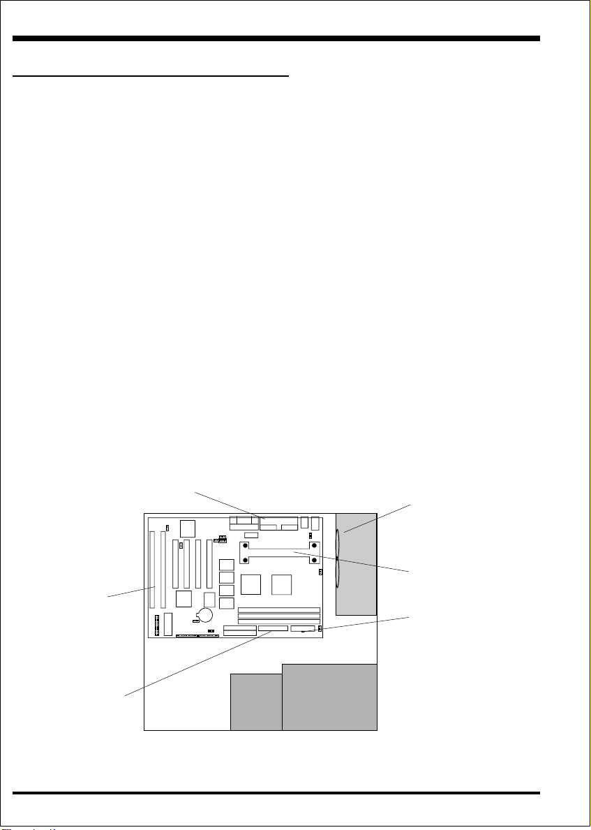
Components Checklist
üü
ü A. (1) EP-BXT mainboard
üü
üü
ü B. (1) EP-BXT user ’s manual
üü
üü
ü C. (1) Floppy ribbon cable
üü
üü
ü D. (1) Hard drive ribbon cables
üü
üü
ü E. (1) Foldable Retention Module
üü
üü
ü F. (1) PS-232 9-PIN ribbon cable
üü
G. (1) PS/2 to AT keyboard connector adapter (optional)
üü
ü H. (1) Bus master drivers
üü
(1) USDM
IntroductionEP-BXT
Section 1
INTRODUCTION
USERS
MANUAL
J4
CPU FAN
EP-BXT
26
A
E
B
F
C
G
D
or
H
Page 1-1
Page 8

Introduction EP-BXT
Overview
Pentium II or Deschutes Processor
The Pentium® II or Deschutes Processor (The Deschutes Processor as 300/
100MHz, 350/100MHz, 400/100MHz and 450/100MHz speed with 512K-L2 cache
Versions.) is the follow-on to the Pentium® Processor. The Pentium® II or
Deschutes Processor, like the Pentium® Pro processor, implements a Dynamic
Execution micro-architecture -- a unique combination of multiple branch prediction,
data flow analysis, and speculative execution. This enables the Pentium® II Processor to deliver higher performance than the Pentium® processor, while maintaining
binary compatibility with all previous Intel architecture processors.
®
A significant feature of the Pentium
perspective, is the built-in direct multiprocessing support. In order to achieve
multiprocessing, and maintain the memory and I/O bandwidth to support it, new
system designs are needed. For systems with dual processors, it is important to
consider the additional power burdens and signal integrity issues of supporting
multiple loads on a high speed bus. The Pentium® II or Deschutes Processor card
supports both uni-processor and dual processor implementations.
®
The Pentium
II or Deschutes Processor utilizes Single Edge Contact (S.E.C.)
(Figure 1) cartridge packaging technology. The S.E.C. cartridge allows the L2 cache
to remain tightly coupled to the processor, while maintaining flexibility when implementing high performance processors into OEM systems. The second level cache is
performance optimized and tested at the cartridge level. The S.E.C. cartridge utilizes
surface mounted core components and a printed circuit board with an edge finger
connection. The S.E.C. cartridge package introduced on the Pentium® II Processor
will also be used in future Slot 1 processors.
II or Deschutes Processor, from a system
The S.E.C. cartridge has the following features: a thermal plate, a cover and a PCB
with an edge finger connection. The thermal plate allows standardized heatsink
attachment or customized thermal solutions. The thermal plate enables a reusable
heatsink to minimize fit issues for serviceability, upgradeability and replacement. The
full enclosure also protects the surface mount components. The edge finger connection maintains socketabilty for system configuration. The edge finger connector is
denoted as ‘Slot 1 connector’ in this and other documentation.
®
The entire enclosed product is called the Pentium
Page 1-2
II or Deschutes Processor. The
Page 9

IntroductionEP-BXT
packaging technology and each of the physical elements of the product are referred
to using accurate technical descriptions. This allows clear reference to the products
as just a processor. This is the model used in past packaging technologies like PGA,
TCP, PQFP, DIP, etc.
S.E.C. Cartridge Terminology
• Pentium® II or Deschutes Processor
The new enclosed card packaging technology is called a “Single Edge
Contact cartridge.” This is similar to previous names for packaging
technology such as PGA or TCP.
• Processor card
The green PCB (with or without components on it)
• Processor core
The silicon on the PLGA package on the PCB
• Cover
The plastic cover on the opposite side from the thermal plate.
• Slot 1
The slot that the S.E.C. cartridge plugs into, just as the Pentium® Pro
processor uses Socket 8.
• Retention mechanism
Formerly ‘retention module’ the dual posts, etc. that holds the cartridge
in place.
• Thermal plate
The heatsink attachment plate.
• Heat sink supports
The support pieces that are
mounted on the mainboard
to provide added support for
heatsinks.
The L2 cache (TagRAM, PBSRAM)
components keep standard industry
names.
®
The Pentium
II or Deschutes Processor
is the first product to utilize the S.E.C.
cartridge technology and Slot 1
connector. Unless otherwise noted, any
references to “Pentium® II Processor,”
Cover
Figure 1: Pentium® II or Deschutes
Processor CPU with S.E.C. Cartridge
Thermal Plate
Processor
Printed Circuit Board
Page 1-3
Page 10

Introduction EP-BXT
“Pentium® II or Deschutes Processor/Slot 1 processor” or “Deschutes Processor”
will apply to both the Pentium® II Processor desktop processors.
Intel740TM Graphics Accelerator
(AGP Onboard)
The EP-BXT is equipped with Intel 740TM Graphics Accelerator Chipset, this chipset
delivers high performance 3D/2D graphics capabilities, and full support for multimedia application. T ypically, 3D graphics rendering, Color Alpha Blending for
Transparency, Real-Time Texture, Fogging and Atmospheric Effects, Specular
Lighting, 1 Buffering... requires a tremendous amount of memory, and demands ever
increasing throughput speed as well. The EP-BXT provides high speed 8M/4M
(optional) SGRAM as well as improving performance and difference display resolutions up to 1600x1200. The Intel740TM Graphics Accelerator is AGP Interface, the
AGP interface is new interface designed for 3D graphics. This interface provides in
Creased bandwith over PCI, fullside band (2X) addressing, and AGP memory 3D
texture storage.
YMF724 PIC Sound
(PCI Audio Onboard)
The EP-BXT is equipped with YMF724 (DS-1) PCI Audio chipset. YMF724 (DS-1)
is a high performance audio controller for the PCI Bus. It consists of two separated
functional blocks. One is the PCI Audio block and the other is the Legacy Audio
block. PCI Audio block allows Software Driver to handle maximum of 72 concurrent audio streams with the Bus Master DMA engine. Legacy Audio block support
OPL3, Sound Blaster Pro, MPU401 UART mode and Joystick function in order to
provied hardware compatibility for PC game in DOS mode.
Hardware Monitoring
Hardware monitoring allows you to monitor various aspects of your systems operations and status. The features include CPU temperature, voltage and RPM of fan.
Page 1-4
Page 11

IntroductionEP-BXT
Page Right Blank
Page 1-5
Page 12
Introduction EP-BXT
EP-BXT Form-Factor
The EP-BXT is designed with ATX form factor - the new industry standard of
chassis. The ATX form factor is essentially a Baby-AT baseboard rotated 90
degrees within the chassis enclosure and a new mounting configuration for the power
supply. With these changes the processor is relocated away from the expansion slots,
allowing them all to hold full length add-in cards. ATX defines a double height
aperture to the rear of the chassis which can be used to host a wide range of
onboard I/O. Only the size and position of this aperture is defined, allowing PC
manufacturers to add new I/O features (e.g.; TV input, TV output, joystick, modem,
LAN, etc.) to systems. This will help systems integrators differentiate their products
in the marketplace, and better meet your needs.
• Smaller size promotes a smaller system size.
• I/O shield does not need to be retooled in an ATX 2.01 or later. Mainboard could
be used in an ATX 2.01-compliant.
• A smaller power supply cam be used. High integration on mainboard reduces the
system costs.
Floppy / IDE
connectors
close to
peripheral
bays
Page 1-6
Expandable I/O
Full length
slots
ATX
Power
J4
CPU FAN
Supply
26
3 1/2"
Bay
Figure 2: Summary of ATX chassis features
5 1/4"
Bay
Single chassis
fan for
system
CPU located near
Power Supply
ATX power
connector
Page 13
IntroductionEP-BXT
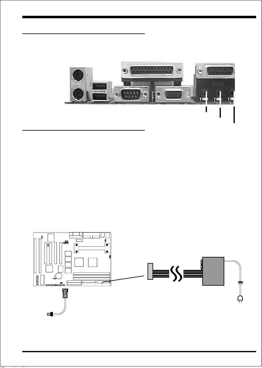
I/O Shield Connector
The EP-BXT is equipped with an I/O back panel. Please use the appropriate I/O
shield (figure 3).
parallel port
Joystick/Midi port
PS/2 Mouse
USB port
PS/2
KEYBOARD
Figure 3: I/O back panel layout
COM1
Power-On/Off (Remote)
VGA1
Speaker
Line_in
MIC
The EP-BXT has a single 20-pin connector for ATX power supplies. For ATX
power supplies that support the Remote On/Off feature, this should be connected to
the systems front panel for system Power On/Off button. The systems power On/
Off button should be a momentary button that is normally open.
The EP-BXT has been designed with “Soft Off" functions. You can turn Off the
system from one of two sources: The first is the front panel Power On/Off the
button, and the other is the "Soft Off" function (coming from the EP-BXT’s onboard
circuit controller) that can be controlled by the operating system. Windows 95/98 will
control this when the user clicks that they are ready to Shutdown the system.
J4
CPU FAN
26
J3
EP-BXT Board
Case (chassis) Power
ON/OFF button
ATX
POWER SUPPLY
Figure 4: Simple ATX Power
ON/OFF Controller
Page 1-7
Page 14
Introduction EP-BXT
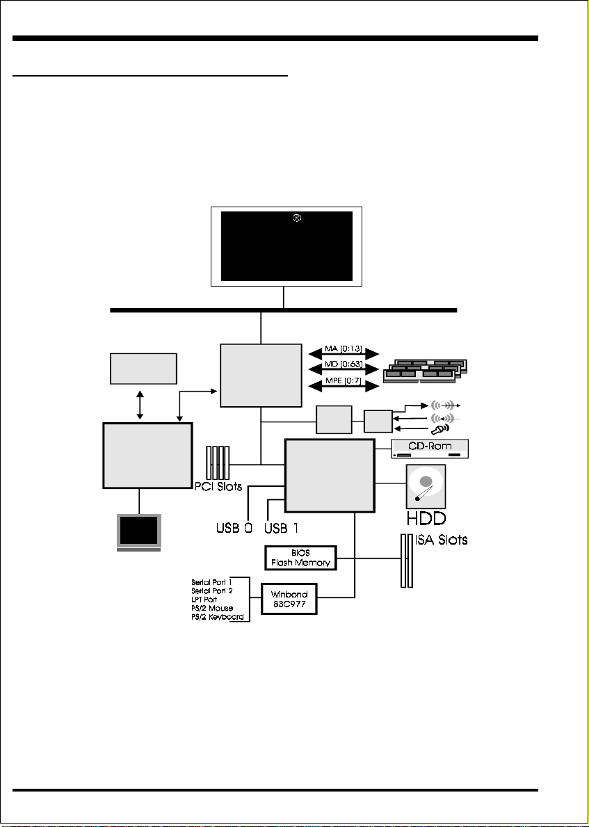
System Block Diagram
P e ntium II or
Deschutes
Processor
100/66MHz
4M/8M
SGRAM
Loc al M em o r y
Intel740
TM
Graphics
Accelerator
PAC
PC I Bridge
and m em ory
controller
443BX
PCI
Sound
PllX4E
I/O B rid g e
AC
97
100/66MHz
Page 1-8
Figure 5: System Block Diagram
Page 15

EP-BXT Features:
FeaturesEP-BXT
Section 2
FEATURES
• EP-BXT is based on the Pentium
at 233 ~ 333MHz (66MHz) or 300 ~450MHz (100MHz) on Slot 1. The
board is configured by an Easy-Setting-Daul-Jumper (E.S.D.J.) to match your
CPU clock speed.
®
II or Deschutes Processor operating
• Designed with Intel’s 82443 BX AGPset.
• Supports up to 768 Mega of DRAM (minimum of 16 MB) on board, You can
use 168-pin DIMM x 3. It will automatically detect Extended Data Output
(EDO) DRAM at 66MHz only or Synchronous DRAM memory (SDRAM) at
66MHz or 100MHz (please see Section 3-2).
• EP-BXT will support Error Checking and Correcting (ECC) when using
paritys DRAM memory modules. This will detect multiple bit errors and
correct 1-bit memory errors.
• Supports (2) 16 bit ISA slots, (4) 32 bit PCI slots, provides (2) independent
high performance PCI IDE interfaces capable of supporting PIO Mode 3/4
and Ultra DMA 33 devices. The EP-BXT supports (4) PCI Bus Master slots
and a jumperless PCI INT# control scheme which reduces configuration
confusion when plugging in PCI card(s).
• Supports ATAPI (e.g. CD-ROM) devices on both Primary and Secondary
IDE interfaces.
• Designed with W inbond W83977TF/EF Multi I/O: (1) floppy port, (1) parallel
port (EPP, ECP), and (2) serial ports (16550 Fast UART).
Note: Japanese “Floppy 3 mode” is also supported
• Includes a PS/2 mouse connector.
• Allows use of a PS/2 keyboard.
• Features Award Plug & Play BIOS. With Flash Memory you can always
upgrade to the current BIOS as they are released.
Page 2-1
Page 16

Features EP-BXT
• EP-BXT utilizes a Lithium battery which provides environmental protec
tion and longer battery life.
• Supports the Universal Serial Bus (USB) connector. The onboard PIIX4E chip
provides the means for connecting PC peripherals such as; keyboards,
joysticks, telephones, and modems.
• Built-in ATX 20-pin power supply connector.
• Software power-down when using Windows
®
95/98.
• Supports ring-in feature (remote power-on through external modem,
allow system to be turned on remotely.
• Resume by Alarm - Allow your system to turn on at a preselected time.
• Power Loss Recovery - In the event of a power outtage your system will
automatically turn itself back on without user intervention.
• Supports CPU Hardware sleep and SMM (System Management Mode).
• Supports Hot key, Any key or password Keyboard power ON function
(KBPO).
• Supports USDM software to offer motherboard various status on Windows
95/98, or Windows® NT 4.0/5.0.
®
• Supports the CPU, PWR and Chassis fan Auto stop in the sleep mode.
• Supports the System Power LED (P ANEL) blinks in the sleep mode.
• Built-in WOL (W ake On Lan) Connector.
• Built-in Intel740TM Graphics Accelerator Onboard to delivers high perfor
mance 3D/2D graphics capabilities.
• Built-in 4M/8M(Optional) SGRAM Local Memory to provides display
resolutions up to 1600x1200
• Built-in Y AMAHA YMF724 PCI Sound Onboard.
• Ture Full Duplex playback and Capture with different Sampling Rate.
• Maximum 64-voice XG captital W ave table
• Synthesizer including GM Compatibility.
• Supports OPL3, Sound Blaster Pro, MPU401 UART mode and Joystick
function.
Page 2-2
Page 17
InstallationEP-BXT
Section 3
INSTALLATION
Page 3-1
Page 18

Installation EP-BXT
EP-BXT Detailed Layout
Bank 0
Bank 1
Mouse
(Top)
Keyboard
(Bottom)
J4
PS/2
JP13
USB
1
USB 1
(Top)
USB 0
(Bottom)
CPU FAN
Bank 2
PWR FAN
J5
COM 1
Parallel Port
VGA1
Game Port
CD3
YMF724-V
1
JP7
Intel
443BX
PCIset
DIMM 1
DIMM 2
SGRAM
512K*32
Battery
JP3
DIMM 3
IDE1
J6
1
JP1
Flash Memory
for BIOS
ESDJ
2
1
5X
3X
5.5X
4.5X4X3.5X
AUTO
66MHz
IDE2
112MHz
100MHz
103MHz
FDD1
Secondary IDE
J3
POWER_ON/OFF
Chassis F AN
IR CONN.
1
KEYLOCK
SPK
RESET
J2
26
25
124MHz
133MHz
CPU Cartridge SLOT 1
1
1
CD2
1
CD1
SGRAM
512K*32
PCI Slot #1
Intel7 40
Chipset
SGRAM
512K*32
TM
SGRAM
512K*32
Winbond
83977
I/Oset
PCI Slot #2
PCI Slot #3
J7:WOL
PCI Slot #4
Intel
PIIX4E
PCIset
ISA Slot #1
ISA Slot #2
Page 3-2
Figure 6
Page 19

InstallationEP-BXT
Easy Installation Procedure
Easy Installation Procedure
The following must be completed before powering on your new system:
3-1. Configure Jumpers to match your hardware
3-2. Install memory chips
3-3. Install Pentium II or Deschutes Processor
3-4. Device Connectors
Section 3-1
Configure Jumpers
The EP-BXT designs all motherboards with the fewest jumpers to make your
installation fast and easy.
The following will describe all of the jumpers that you are required to set before
moving on to step 3-2.
Note: The jumpers as depicted as shown (Figure 6) in their correct physical
orientation.
JP1 CMO S C lear
1
JP1 = 1-2 - Run Mode (Default)
3
JP7 PCI Sound (O nboard Sound Chip)
1
= 2-3 - Clear CMO S (momentarily)
JP7 = 1-2 - Enabled PC I Soun d (Default)
3
1
JP13 K eyboard P ow er-ON function (refer to the sec
= 2-3 - Disab le d P CI So u n d
JP 1 3 = 1-2 - Ena b led
3
= 2-3 - Disab le d(Defa u lt)
J7 WO L (Wak e O n L an) C onnector
R eserved for N IC (N etwork Interface C ard ) to
Wake the System.
Page 3-3
Page 20
Installation EP-BXT
*
*
*
*
*
**
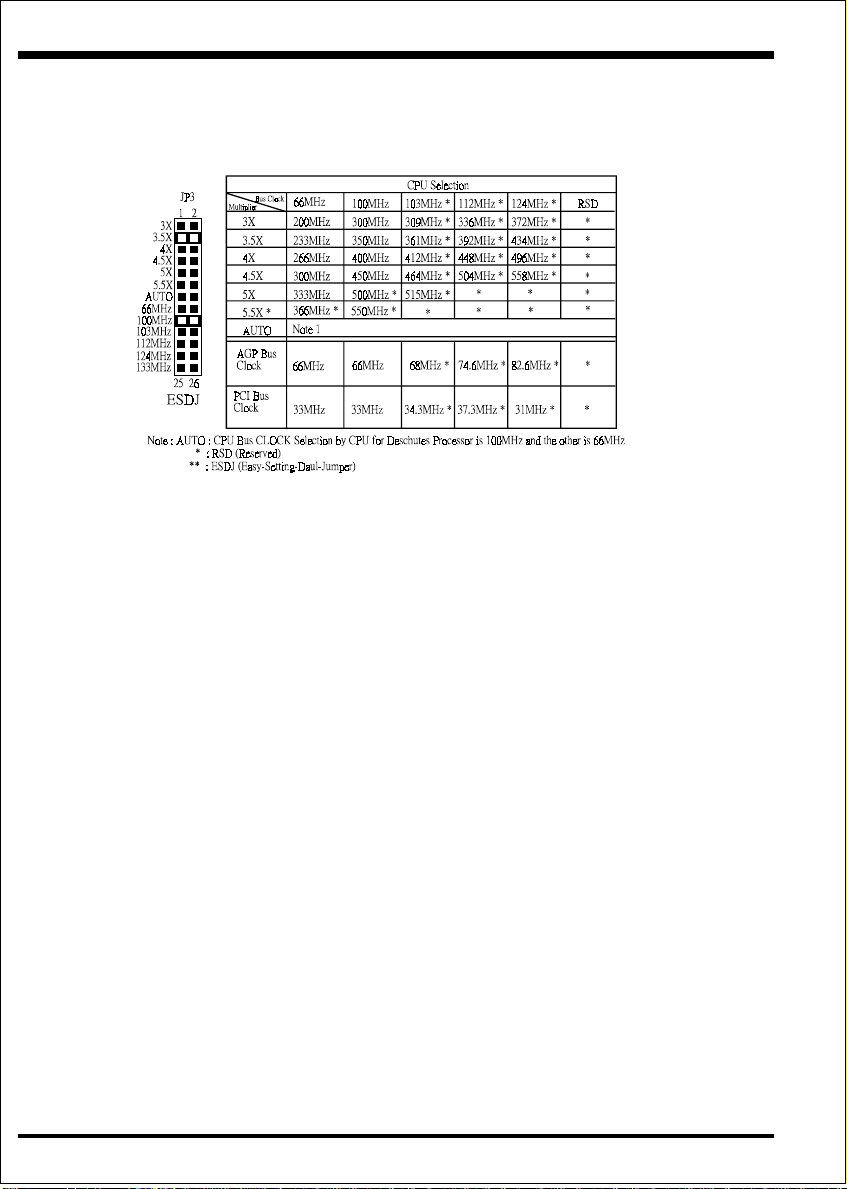
Note: Based on the implementation of Intel 440BX PCIset, EP-BXT is able to
provide two host bus frequencies -- either 66 or 100MHz for Slot1 processor
and memory operating. The default is set at 100MHz once Pentium® II
processor to be mounted onto this mainboard. However, no matter what kind
of Slot1 processor you installed, it should come with right memory modules
for normal and stable operation. For example, if you install a Deschutes
processor, you should use the SDRAM module with 100MHz based(or above)
to match the CPU speed. Furthermore, one thing you may need to bear in
mind, before the CPU installation, it is anyway our advice to use JP3 and set
up right speed of Slot1 processor at any time.
Page 3-4
Page 21

InstallationEP-BXT
Section 3-2
System Memory Configuration
Memory Layout
The EP-BXT supports (3) 168-pin DIMMs (Dual In-line Memory Module). The
DIMMs can be either EDO (Extended Data Out) or SDRAM (Synchronized
DRAM).
• We recommend using SDRAM DIMM can not mixing
with EDO DIMM modules together at 66MHz.
• The EDO DIMM only support pentium
support Deschutes Processor at 100MHz.
• 256MB only Support Registered synchronous DRAM Memory
Modules. The Registered SDRAM DIMM do not mix with SDRAM
DIMM modules together.
• We recommend when installed the 100MHz Deschutes Processor
using DIMM SDRAM must be 125MHz (-8ns) bus speed. If used
100MHz (-10ns) SDRAM may be critical timing for the
motherboard.
• About the “PC/100 SDRAM spec.” information you may visit Intel’s
home page at:
http//developer.intel.com/design/pcisets/memory/index.htm
• DIMM SDRAM may be 83MHz (-12ns), 100MHz (-10ns) or
125MHz (-8ns) bus speed.
Figure 2 and Table 1 show several possible memory configurations using
®
II Processor at 66MHz, not
DIMM 1 (M1)
DIMM 2 (M2)
DIMM 3 (M3)
Figure 2
Bank 0
Bank 1
Bank 2
-Synchronous
-SDRAM or EDO
DIMM
Page 3-5
Page 22
Installation EP-BXT
yromeMlatoT
BM867=
mumixaM
BM215=
mumixaM
BM652=
mumixaM
1X
1X
1X
1MMID
)0knaB(
*MARDS/ODE
,BM23,BM61,BM8
BM652,BM821,BM46
1X
*MARDS/ODE
,BM23,BM61,BM8
BM652,BM821,BM46
1X
*MARDS/ODE
,BM23,BM61,BM8
enoNenoN
BM652,BM821,BM46
2MMID
)1knaB(
*MARDS/ODE
,BM23,BM61,BM8
BM652,BM821,BM46
1X
*MARDS/ODE
,BM23,BM61,BM8
enoN
BM652,BM821,BM46
3MMID
)2knaB(
*MARDS/ODE
,BM23,BM61,BM8
Table 1
*SDRAM only supports 8, 16, 32, 64, 128MB DIMM modules. 256MB only
supports Registered Synchronouts DRAM Memory Modules.
* EDO only supports Pentium® II Processor at 66MHz, not supports Deschutes
Processor at 100MHz.
DIMM Module Installation
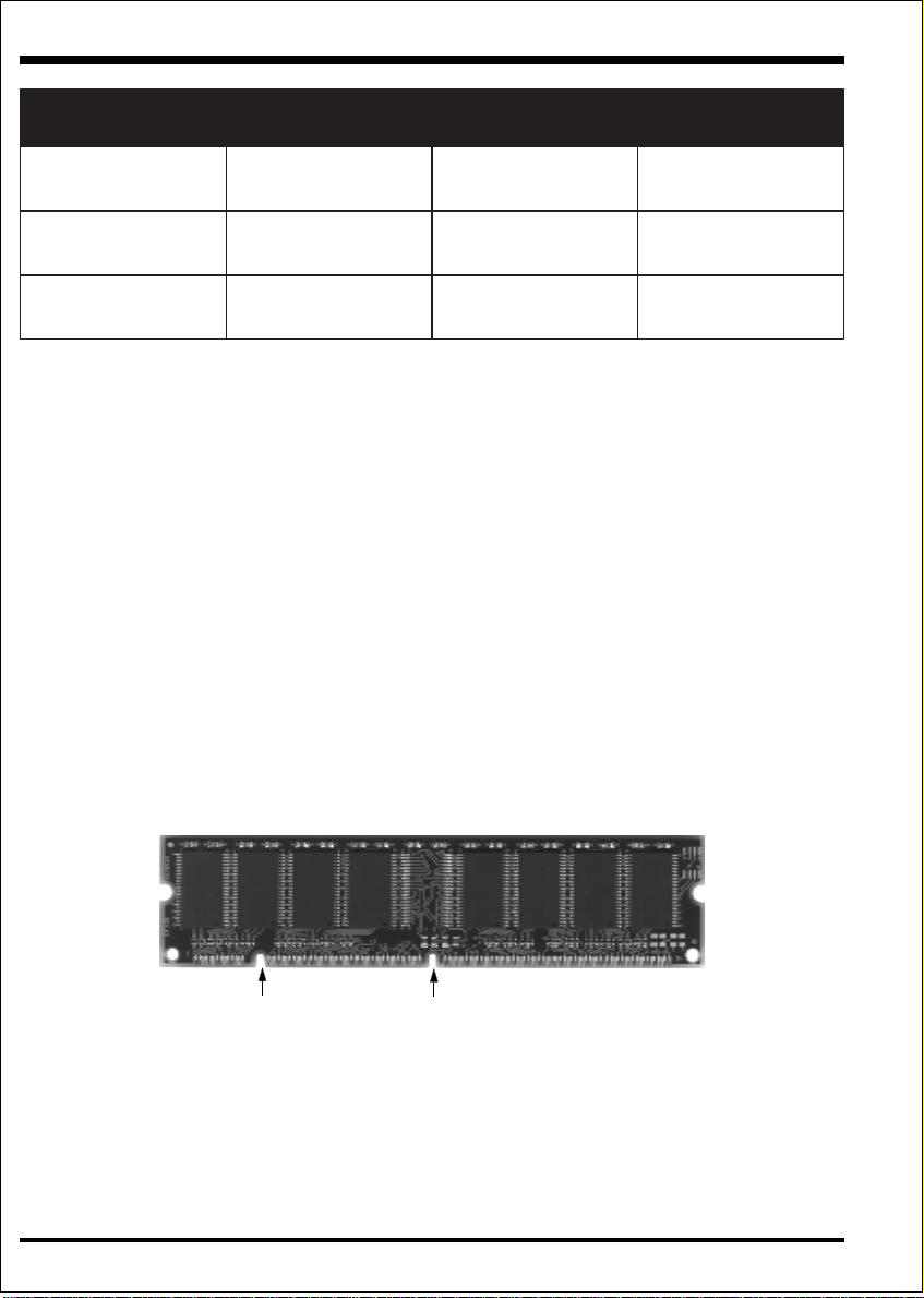
Figure 7 displays the notch marks and what they should look like on your DIMM
memory module.
DIMMs have 168-pins and two notches that will match with the onboard DIMM
socket. DIMM modules are installed by placing the chip firmly into the socket at a
90 degree angle and pressing straight down (figure 8) until it fits tightly into the
DIMM socket (figure 9).
BM652,BM821,BM46
Page 3-6
LEFT KEY ZONE
(UNBUFFERED)
CENTER KEY ZONE
(3.3 V DRAM)
Figure 7
Page 23

Figure 8
DIMM Module clip before installation
Figure 9
DIMM Module clip after installation
InstallationEP-BXT
To remove the DIMM module simply press down both of the white clips on either
side and the module will be released from the socket.
Page 3-7
Page 24

Installation EP-BXT
Section 3-3
®®
®
Installing a Pentium
The EP-BXT uses the Single Edge Contact (SEC) slot for a Pentium® II processor
packaged in an SEC cartridge. The SEC slot is not compatible with other nonPentium II processors.
Please have ready the following list of components so that we may install the
processor onto the motherboard.
1. Pentium II processor heat sink
2. Intel Pentium II Processor
OK, now that you have all of your components ready, we can start.
First, please refer to figure 10 below, and follow the direction to lift up the fixed
foldable pentium
designed for you to install Pentium® II CPU more easier and to avoide any
damage on the board due to overtightening the four screws.
One thing must be kept in your mind that please make sure to lift upright the
foldable parts of the Retention module to fit and install CPU properly.
®
II Retention Mechanism. This pre-installed device is
®®
II or Deschutes Processor
Figure 10
Now we are ready to install the SEC Cartridge (Pentium II Processor) into the
Retention Module. The SEC Cartridge is mounted by sliding the SEC Cartridge into
the Retention Module and letting it slide all the way down. Once it reaches the
bottom make sure you press firmly on SEC cartridge to firmly secure into the Slot 1
Socket.
Page 3-8
Page 25

CPU Installation procedure:
Figure 1-2: Please lift up right the folderabled reteation.
InstallationEP-BXT
Figure 3-4: Press and slide down the processor into slot 1 connector to secure
a Pentium
®
II processor
Page 3-9
Page 26

Installation EP-BXT
Section 3-4
Device Connectors
Please install the motherboard into the chassis.
Now that your motherboard is installed you are ready to connect all your connections (figure 14).
PS/2 Mouse
PS/2
KEYBOARD
USB port
COM1 VGA1
Figure 14
J2,J3: Chassis Panel Connector
• Keylock, Speaker, Reset, Sleep, Turbo LED and HDD LED
J4: CPU Fan Power
• A plug-in for the CPU Fan Power
J5: Power Supply Fan Monitoring
• A plug-in for the Power supply so that BIOS can monitor the RPM’s
J6: Chassis Fan Power
• A plug-in for the chassis Fan Power
J7: WOL (Wake On Lan) Connector
PW2: ATX Power Connector
• 20-pin power connector
IDE1: Primary IDE Connector
IDE2: Secondary IDE Connector
FDD1: Floppy Controller Connector
CD1: MITSUMI CD-ROM Audio_in
CD2: SONY CD-ROM Audio_in
CD3: Panasonic CD-ROM Audio_in
parallel port
Joystick/Midi port
Speaker
Line_in
MIC
Page 3-10
Page 27

Section 3-4
Device Connectors (continued)
InstallationEP-BXT
J2
J3 1
+
+
Reset - Closed to restart system.
1
Speaker - Connect to the system's speaker for beeping
1. Speaker 3. GND
2. N/C 4. GND
KeyLock - Keyboard lock switch & Power LED connector
1. Power LED(+) 4. Keylock
2. N/C 5. GND
3. GND
* The power LED lights when the
system is powered on and blinks in
SLEEP MODE (Suspend mode).
IR Connector
1. VCC 4. GND
2. NC 5. IRTX
3. IRRX
IDE LED indicator - LED ON when Onboard PCI IDE Hard disks is
activate
Turbo LED indicator - LED ON when higher speed is selected
Power On/Off - This is connected to the power button on the case.
Using the Soft-Off by Pwr-BTTN feature, you can choose either Instant
Off (turns system off immediatly), or 4 sec delay (you need to hold the
button down for 4 seconds before the system turns off). When the
system is in 4 sec delay mode, there is a special feature to make the
system to go into suspend mode when the button is pressed
momentarily.
Page 3-11
Page 28

Installation EP-BXT
Section 3-5
External Modem Ring-in Power
ON and Keyboard Power ON
Functions (KBPO)
On the basis of bounded functions in I/O chipset, the two serial ports are able to
support the External Modem Ring-in Power ON function. Once users connect the
external modem to COM1 or COM2, the EP-BXT mainboard allows users to turn on
their system through the remote and host's dial-up control.
Exclusive Keyboard Power ON Function
To innovate a unique feature to benefit users, we devoted the easiest and most
convenient way to turn on your system based on the the ATX power supply.
How to work with it
Step 1:Please check JP13 at the position 1-2 after you finished the system
installation.
JP13 K eyboard P ower-O N Function Selection
1-2 : E nabled
2-3 : Disabled (Default)
Step 2:Push the momentary switch (J3 PW-ON) to turn on your system and then
push again to hold for more than 4 seconds to turn it off affter counting
memory as soon as you turn it on.
Step 3:You can enjoy the Keyboard Power ON function (KBPO) by pressing any 1
key, Hot key (Ctrl-F1, F2.....F12), Password (A maximum of 5 charac
ters can be entered.) and BUTTON only to turn on your system. Please refer
to the BIOS Integrated peripherals setup for detail (Page 4-23).The BIOS
Default is keyboard Hot key <Ctrl> - <F1> to turn on the system. Your
system will be turned on automatically, after releasing the keys. To power off
you system, you can use the Soft-OFF function under Windows 95.
Page 3-12
Page 29

Notes:
1.Intel ATX version 2.0 specification has recommended you use the
power supply with 0.72A(720mA) in 5.0VSB. With our EP-BXT
mainboard, the 5.0VSB standby power only has to be > = 0.1A
(100mA) then you can enjoy this unique benefit. However, the ATX
power supply which is < 0.1 (100mA) is still applicable to your system
by placed JP13 at the position 2-3 to disable this feature.
InstallationEP-BXT
Page 3-13
Page 30

Installation EP-BXT
Page Left Blank
Page 3-14
Page 31

BIOSEP-BXT
Section 4
AWARD BIOS SETUP
BIOS Instructions
Award’s ROM BIOS provides a built-in Setup program which allows user to modify
the basic system configuration and hardware parameters. The modified data will be
stored in a battery-backed CMOS, so that data will be retained even when the power
is turned off. In general, the information saved in the CMOS RAM will stay unchanged unless there is a configuration change in the system, such as hard drive
replacement or a device is added.
It is possible for the CMOS battery to fail, this will cause data loss in the CMOS
only. If this does happen you will need to reconfigure your BIOS settings.
To enter the Setup Program :
Power on the computer and press the <Del> key immediately, this will bring you into
the BIOS CMOS SETUP UTILITY.
ROM PCI / ISA BIOS (2A69KPAB)
CMOS SETUP UTILITY
AWARD SOFTWARE, INC.
STANDARD CMOS SETUP SUPERVISOR PASSWORD
BIOS FEATURES SETUP USER PASSWORD
CHIPSET FEATURES SETUP IDE HDD AUTO DETECTION
POWER MANAGEMENT SETUP HDD LOW LEVEL FORMAT
PNP/PCI CONFIGURATION SAVE & EXIT SETUP
INTEGRATED PERIPHERALS EXIT WITHOUT SAVING
LOAD SETUP DEFAULTS
éé
é
éé
êê
èè
çç
ê
è
ç
êê
èè
ESC : QUIT : SELECT ITEM
F10 : Save & Exit Setup (Shift)F2 : Change Color
Time, Date, Hard Disk Type...
çç
Figure 1: CMOS Setup Utility
Page 4-1
Page 32

BIOS EP-BXT
The menu displays all the major selection items. Select the item you need to
reconfigure. The selection is made by moving the cursor (press any direction key ) to
the item and pressing the ‘Enter’ key. An on-line help message is displayed at the
bottom of the screen as the cursor is moved to various items which provides a better
understanding of each function. When a selection is made, the menu of the selected
item will appear so that the user can modify associated configuration parameters.
4-1 Standard CMOS Setup
Choose “Standard CMOS Setup” in the CMOS SETUP UTILITY Menu (Figure 2).
The Standard CMOS Setup allows the user to configure system settings such as the
current date and time, type of hard disk drive installed, floppy drive type, and display
type. Memory size is auto-detected by the BIOS and displayed for your reference.
When a field is highlighted (use direction keys to move the cursor and the <Enter>
key to select), the entries in the field can be changed by pressing the <PgDn> or the
<PgUp> key.
ROM PCI/ISA BIOS(2A69KPAB)
STANDARD CMOS SETUP
AWARD SOFTWARE, INC.
Date (mm:dd:yy) : Wed, Apr 17 1996
Time (hh:mm:ss) : 14 : 30 : 50
HARD DISKS TYPE SIZE CYLS HEAD PRECOMP LANDZONE SECTORS MODE
Primary Master : Auto 0 0 0 0 0 0 Auto
Primary Slave : Auto 0 0 0 0 0 0 Auto
Secondary Master : Auto 0 0 0 0 0 0 Auto
Secondary Slave : Auto 0 0 0 0 0 0 Auto
Drive A : 1.44M, 3.5 in.
Drive B : None
Floppy 3 Mode Support : Disabled
Video : EGA/VGA
Halt On : All Errors
éé
é
éé
êê
èè
çç
ê
è
ç
êê
èè
ESC : Quit : Select Item PU/PD/+/- : Modify
F1 : Help (Shift) F2 : Change Color
çç
Base Memory : 640K
Extended Memory : 31744K
Other Memory : 384K
Total Memory : 32768K
Figure 2: Standard CMOS Setup
NOTE: If the hard disk Primary Master/Slave and Secondary Master/Slave
are set to Auto, then the hard disk size and model will be auto-detected.
Page 4-2
Page 33

BIOSEP-BXT
NOTE: The “Halt On:” field is used to determine when to halt the system
by the BIOS if an error occurs.
NOTE: Floppy 3 Mode support is a mode used to support a special 3.5”
drive used in Japan. This is a 3.5” disk that stores only 1.2 MB, the default
setting for this is disabled.
4-2 BIOS Features Setup
Selecting the “BIOS FEATURES SETUP” option in the CMOS SETUP UTILITY
menu allows users to change system related parameters in the displayed menu. This
menu shows all of the manufacturer’s default values for the EP-BXT.
Pressing the [F1] key will display a help message for the selected item.
ROM PCI/ISA BIOS(2A69KPAB)
BIOS FEATURES SETUP
AWARD SOFTWARE, INC.
Virus Warning : Disabled Video BIOS Shadow : Enabled
CPU Internal Cache : Enabled C8000-CBFFF Shadow : Disabled
External Cache : Enabled CC000-CFFFF Shadow : Disabled
Quick Power On Self Test : Enabled D0000-D3FFF Shadow : Disabled
Boot Sequence : A, C, SCSI D4000-D7FFF Shadow : Disabled
Swap Floppy Drive : Disabled D8000-DBFFF Shadow : Disabled
Boot Up Floppy Seek : Enabled DC000-DFFFF Shadow : Disabled
Boot Up NumLock Status : On
Boot UP System Speed : High
Gate A20 option : Fast
Typematic Rate Setting : Disabled
Typematic Rate (Chars/Sec) : 6
Type matic Delay (Msec) : 250
Security Option : Setup
PCI/VGA Palette Snoop : Disabled
Assign IRQ For VGA : Enabled
OS Select For DRAM > 64MB : Non-OS2
Report NO FDD For Win 95 : NO
Esc : Quit : Select Item
F1 : Help PU/PD/+/- : Modify
F5 : Old Values (Shift) F2 : Color
F7 : Load Setup Defaults
éé
é
éé
êê
èè
çç
ê
è
ç
êê
èè
çç
Figure 3: BIOS Features Setup
Virus Warning: During and after the system boots up, any attempt to write to the
boot sector or partition table of the hard disk drive will halt the system and an error
message will appear.
You should then run an anti-virus program to locate the virus. Keep in mind that this
feature protects only the boot sector, not the entire hard drive.
The default value is Disabled.
Page 4-3
Page 34

BIOS EP-BXT
Enabled: Activates automatically when the system boots up causing a
warning message to appear when anything attempts to access the boot
sector.
Disabled: No warning message will appear when anything attempts to
access the boot sector.
Note: Many disk diagnostic programs that access the boot sector table can
trigger the virus warning message. If you plan to run such a program, we
recommend that you first disable the virus warning.
CPU Internal Cache: This controls the status of the processor’s internal cache
area.
The default is Enabled.
Enabled: This activates the processor’s internal cache thereby increasing
performance.
Disabled: This deactivates the processor’s internal cache thereby lowering
performance.
External (L2) Cache: This controls the status of the external (L2) cache area.
The default is Enabled.
Enabled: This activates the motherboard’s L2 cache thereby increasing
performance.
Disabled: This deactivates the motherboard’s L2 cache thereby lowering
performance.
Quick Power On Self Test: This category speeds up the Power On Self Test
(POST).
The default is Enabled.
Enabled: This setting will shorten or skip of the items checked during
POST.
Disabled: Normal POST.
Boot Sequence: This category determines which drive is searched first by the O/S
(Operating System).
The default is A,C,SCSI.
The following is your list of options:
[A, C, SCSI] - [C, A, SCSI] - [C, CD-ROM, A] - [CD-ROM, C, A]
[D, A,CD-ROM],[E, A, CD-ROM] - [F, A, CD-ROM] - [SCSI, A, C]
[SCSI C, A] - [C Only]
Page 4-4
Page 35

BIOSEP-BXT
Swap Floppy Drive: This will swap your physical drive letters A & B if you are
using two floppy disks.
The default is Disabled.
Enabled: Floppy A & B will be swapped under the O/S.
Disabled: Floppy A & B will be not swapped.
Boot Up Floppy Seek: During Power-On-Self-Test (POST), BIOS will determine
if the floppy disk drive installed is 40 or 80 tracks. Only 360K type is 40 tracks while
760K, 1.2MB and 1.44MB are all 80 tracks.
The default is Enabled.
Enabled: The BIOS will search the floppy disk drive to determine if it is 40
or 80 tracks.
Disabled: The BIOS will not search for the type of floppy disk drive by
track number.
NOTE: BIOS can not tell the difference between 720K, 1.2MB and 1.
44MB drive types as they are all 80 tracks.
Boot Up NumLock Status: This controls the state of the NumLock key when the
system boots.
The default is On.
On: The keypad acts as a 10-key pad.
Off: The keypad acts like the cursor keys.
Boot UP System Speed: This controls the initial system speed of the computer.
The default is High.
High: This setting sets the computer into normal operation mode.
Low: This setting sets the computer into a slower operating mode. Some
add-in peripherals or old software may require this setting. Using
CTRL+ALT+(+) will switch you back into high speed mode.
Gate A20 Option: This refers to the way the system addresses memory above
1MB (extended memory).
The default is Fast.
Normal: The A20 signal is controlled by the keyboard controller or chipset
hardware.
Fast: The A20 signal is controlled by Port 92 or chipset specific method.
Page 4-5
Page 36

BIOS EP-BXT
Typematic Rate Setting: This determines the keystrokes repeat rate.
The default is Disabled.
Enabled: Allows typematic rate and typematic delay programming.
Disabled: The typematic rate and typematic delay will be controlled by the
keyboard controller in your system.
Typematic Rate (Chars/Sec) : This is the number of characters that will be repeated by a keyboard press.
The default is 6.
6: 6 characters per second. 8: 8 characters per second.
10: 10 characters per second. 12: 12 characters per second.
15: 15 characters per second. 20: 20 characters per second.
24: 24 characters per second. 30: 30 characters per second.
Typematic Delay (msec): This setting controls the time between the first and the
second character displayed by typematic auto-repeat.
The default is 250.
250: 250 msec.
500: 500 msec.
750: 750 msec.
1000: 1000 msec.
Security Option: This category allows you to limit access to the System and Setup,
or just to Setup.
The default is Setup.
System: The system will not boot and the access to Setup will be denied if
the correct password is not entered at the prompt.
Setup: The system will boot; but the access to Setup will be denied if the
incorrect password is not entered at the prompt.
PCI/VGA Palette Snoop: This field controls the ability of a primary PCI VGA
controller to share a common palette (When a snoop write cycles) with an ISA video
card.
The default is Disabled.
Enabled: If an ISA card is connected to a PCI VGA card via the VESA
connector, and that ISA card connects to a VGA monitor, then that ISA card
uses the RAMDAC of the PCI card.
Disabled: Disables the VGA card Palette Snoop function.
Page 4-6
Page 37

BIOSEP-BXT
Assign IRQ For VGA: This option allows BIOS to assign IRQ for VGA device
Enabled: The system was assigned IRQ for VGA Card.
Disabled: The system was not assigned IRQ for VGA Card.
OS Select For DRAM > 64MB: Some operating systems require special handling.
Use this option only if your system has greater than 64MB of memory.
The default is Non-OS2.
OS2: Select this if you are running the OS/2 operating system with greater
than 64MB of RAM.
Non-OS2: Select this for all other operating systems and configurations.
Report No FDD For WIN95: This option allows BIOS to indicate whether
WIN95 is with FDD or not. The Default value is NO.
NO: Report No FDD for WIN95.
YES: Report FDD for WIN95
Video BIOS Shadow: This option allows video BIOS to be copied into RAM.
Video Shadowing will increase the video performance of your system.
The default is Enabled.
Enabled: Video shadow is enabled.
Disabled: Video shadow is disabled.
C8000 - CBFFF Shadow:
CC000 - CFFFF Shadow:
D0000 - D3FFF Shadow:
D4000 - D7FFF Shadow:
D8000 - DBFFF Shadow:
DC000 - DFFFF Shadow:
These categories determine whether ROMs from option cards will be copied into
RAM. This will be in 16K byte or 32K byte units, and the size will depend on chipset
of the option card.
Enabled: Optional shadow is enabled.
Disabled: Optional shadow is disabled.
Page 4-7
Page 38

BIOS EP-BXT
4-3 Chipset Features Setup
Choose the “CHIPSET FEATURES SETUP” in the CMOS SETUP UTILITY
menu to display following menu.
ROM PCI/ISA BIOS(2A69KPAB)
CHIPSET FEATURES SETUP
AWARD SOFTWARE, INC.
Auto Configuration : Enabled Auto Detect DIMM/PCI Clk : Enabled
EDO DRAM Timing : 60ns Spread Spectrum Modulated : Enabled
EDO CASx# MA wait state : 2 Current cpu Temperature : 31C/87F
EDO RAS Wait State : 2 Current System Temp : 31C/87F
SDRAM CAS LATENCY Time : 3 Current PWR SUP FAN Speed : 0 RPM
DRAM Data Integrity Mode : Non-ECC Current CPU FAN Speed : 5578 RPM
System BIOS Cacheable : Enabled Current Chiassis FAN Speed : 0 RPM
Video BIOS Cacheable : Enabled Vcore : 2.08 V Vtt : 1.55 V
Video RAM Cacheable : Enabled Vio : 3.36 V +5V : 5.16 V
8 Bit I/O Recovery Time : 1 +12V : 12.28 V -12V : 11.90 V
16 Bit I/O Recovery Time : 1 -5V : 5.20 V
Memory Hole At 15M-16M : Disabled
Passive Release : Enabled
Delayed Transaction : Disabled
AGP Aperture Size (MB) : 64
CPU Warning Temperature : 60C/140F
éé
é
éé
êê
èè
çç
ê
è
ç
êê
èè
Esc : Quit : Select Item
F1 : Help PU/PD/+/- : Modify
F5 : Old Values (Shift) F2 : Color
F7 : Load Setup Defaults
çç
Figure 4: Chipset Features Setup
Auto Configuration: This selects predetermined optimal values of the chipset
parameters.
The default is Enabled.
Enabled: This enables auto-configuration and provides the option to select
predefined timing modes.
Disabled: This allows the user to specify DRAM timing parameters.
Note: If you exceed the performance characteristics of memory in your
system it will result in lockups, crashes and other problematic system
operations.
EDO DRAM Speed Selection: This value must correspond to the speed of the
DRAM installed in your system.
®
The default is 60ns. This item is for EDO DIMM in Pentium
II processor at 66MHz
only.
Page 4-8
Page 39

BIOSEP-BXT
50ns: (Faster) Burst Wait State, for 50ns EDO DRAM.
60ns: (Slower) Burst Wait State, for 60ns Fast Page Mode/EDO DRAM.
EDO CASx# MA Wait State: This allows the option to insert an additional wait
state before the assertion of the first CASx# for page hit cycle.
The default is 2.
1: Inserts one wait state.
2: Inserts two wait states.
EDO RASx# Wait State: This allows the option to insert an additional wait state
before RAS# is asserted for row misses.
1: Inserts one wait state.
2: Inserts two wait states.
SDRAM CAS Latency Time: This setting defines the CAS timing parameter of
the SDRAM in terms of clocks.
The default is 3.
2: Provides faster memory performance.
3: Provides better memory compatibility.
System BIOS Cacheable: This allows you to copy your BIOS code from slow
ROM to fast RAM.
The default is Enabled.
Enabled: The option will improve system performance. However, if any
program writes to this memory area, a system error may result.
Disabled: System BIOS non-cacheable.
Video BIOS Cacheable: This option copies the video ROM BIOS to fast RAM
(C0000h to C7FFFh).
The default is Enabled.
Enabled: Enables the Video BIOS Cacheable to speed up the VGA
Performance.
Disabled: Will not use the Video BIOS Cacheable function.
Page 4-9
Page 40

BIOS EP-BXT
Video RAM Cacheable: This option allows the CPU to cache read/writes of the
video RAM.
The default is Enabled.
Enabled: This option allows for faster video access.
Disabled: Reduced video performance.
8 Bit I/O Recovery Time: This function allows you to set the wait state that is
added to an 8 bit ISA instruction originated by the PCI bus.
The default is 3.
NA: No wait state 8: 8 wait states
1: 1 wait states 2: 2 wait states
3: 3 wait states 4: 4 wait states
5: 5 wait states 6: 6 wait states
7: 7 wait states
16 Bit I/O Recovery Time: This function allows you to set the wait state that is
added to an 16 bit ISA instruction originated by the PCI bus.
The default is 2.
NA: No wait state 4: 4 wait states
3: 3 wait states 2: 2 wait states
1: 1 wait states
Memory Hole at 15M-16M: You can reserve this memory area for the use of
ISA adaptor ROMs.
The default is Disabled.
Enabled: This field enables the main memory (15~16MB) to remap to ISA
BUS.
Disabled: Normal Setting.
NOTE: If this feature is enabled you will not be able to cache this
memory segment.
Passive Release: This option allows access from the CPU to PCI bus to be active
during passive release. Otherwise, the arbiter only accepts another PCI master
access to local DRAM.
The default is Enabled.
Enabled: Enabled
Disabled: Disabled
Page 4-10
Page 41

BIOSEP-BXT
Delayed Transaction: This option allows the chipset to use its embedded 32-bit
posted write buffer to support delay transactions cycles.
The default is Disabled.
Enabled: Select enabled to support PCI 2.1 specification.
Disabled: Disabled.
AGP Aperture Size: The amount of system memory that the AGP card is allowed
to share.
The default is 64.
4: 4MB of systems memory accessable by the AGP card.
8: 8MB of systems memory accessable by the AGP card.
16: 16MB of systems memory accessable by the AGP card.
32: 32MB of systems memory accessable by the AGP card.
64: 64MB of systems memory accessable by the AGP card.
128: 128MB of systems memory accessable by the AGP card.
256: 256MB of systems memory accessable by the AGP card.
Auto Detect DIMM/PCI Clk: Allows you to stop DIMM/PCI Clock drive when
the DIMM site or PCI Slot are not plug. This item may help reduce EMI.
The default is Enabled.
Enabled: Provides unused DIMM/PCI to stop.
Disabled: Provides the clock generator always driving.
Spread Spectrum Modulated: Allows you to active the Spread Spectrum Modulation function for reduce EMI. (Note: When Enabled the item that performance will
be impacted).
The default is Enabled.
Enabled: Provides the Spread Spectrum function from clock generator.
Disabled: NO Spread Spectrum function.
CPU Warning Temperature: This is the temperature that the computer will
respond to an overheating CPU.
The default is Disabled.
Enabled: Temperature is monitored on the CPU
Disabled: This feature is turned off.
Current CPU Temperature: This is the current temperature of the CPU.
Current Power FAN Speed: The current power fan speed in RPMs.
Page 4-11
Page 42

BIOS EP-BXT
Current CPU FAN Speed: The current CPU fan speed in RPMs.
Current Chassis FAN Speed: The current chassis fan speed in RPMs.
Vcore: The voltage level of the CPU.
Vtt: The voltage level of the CPU’s GTL+ Bus.
+5V, +12V: The voltage level of the switch power supply.
Vio,
4-4 Power Management Setup
Choose the “POWER MANAGEMENT SETUP” in the CMOS SETUP UTILITY
to display the following screen. This menu allows the user to modify the power
management parameters and IRQ signals. In general, these parameters should not be
changed unless it’s absolutely necessary.
ROM PCI/ISA BIOS ((2A69KPAB)
POWER MANAGEMENT SETUP
AWARD SOFTWARE, INC.
ACPI Function : Enabled
Power Management : User Define ** Reload Global Timer Events **
PM Control by APM : Yes IRQ [3-7, 9-15], NMI : Enabled
Video off Method : V/H SYNC+Blank Primary IDE 0 : Disabled
Video off After : Standby Primary IDE 1 : Disabled
Modem Use IRQ : 3 Secondary IDE 0 : Disabled
Doze Mode : Disabled Secondary IDE 1 : Disabled
Standby Mode : Disabled Floppy Disk : Disabled
Suspend Mode : Disabled Serial Port : Disabled
HDD Power Down : Disabled Parallel Port : Disabled
Throttle Duty Cycle : 62.5%
VGA Active Monitor : Enabled
Soft-off by PWB-BTTN : Delay 4 Sec.
Resume by Alarm : Enabled
Power Loss Recovery : Enabled
Resume By Alarm : Enabled
Date (of Month) Alarm : 0
Time (hh:mm:ss) Alarm : 8: 0 :0
IRQ 8 Clock Event : Disabled
Esc : Quit : Select Item
F1 : Help PU/PD/+/- : Modify
F5 : Old Values (Shift) F2 : Color
F7 : Load Setup Defaults
éé
é
éé
êê
èè
çç
ê
è
ç
êê
èè
çç
Figure 5: Power Management Setup
You can only change the content of Doze Mode, Standby Mode, and Suspend Mode
when the Power Management is set to ‘User Define’.
ACPI Function: This option allows you to select ACPI Function.
The default is Enabled.
Enabled: Support ACPI function for new O.S
Disabled: No Support ACPI function.
Page 4-12
Page 43

BIOSEP-BXT
Power Management: Use this to select your Power Management selection.
The default is User define.
Disabled: The system operates in NORMAL conditions (Non-GREEN), and
the Power Management function is disabled.
Max. saving: Maximum power savings. Inactivity period is 1 minute in each
mode.
Min. saving: Minimum power savings. Inactivity period is 1 hour in each
mode.
User define: Allows user to define PM Timers parameters to control power
saving mode.
PM controlled APM: This option shows whether or not you want the Power
Management to be controlled the Advanced Power Management (APM).
The default is Yes.
Yes: APM controls your PM
No: APM does not control your PM
Video Off Method: This option allows you to select how the video will be disabled
by the power management.
The default is V/H Sync + Blank
V/H Sync + Blank: System turns off vertical and horizontal synchronization
ports and writes blanks to the video buffer.
DPMS: Select this option if your monitor supports the Display Power
Management Signaling (DPMS) standard of the Video Electronics Standards Association (VESA). Use the software supplied for your video subsystem to select video power management values.
Blank Screen: System only writes blanks to the video buffer.
Video Off After: Tells you what time frame that the video will be disabled under
current power management settings.
The default is Standby.
Standby: Video powers off after time shown in standby mode setting.
Doze: Video powers off after time shown in doze mode setting.
Suspend: Video powers off after time shown in suspend mode setting.
N/A: Video power off not controlled by power management.
Page 4-13
Page 44

BIOS EP-BXT
MODEM Use IRQ: Name the interrupt request (IRQ) line assigned to the modem
(if any) on your system. Activity of the selected IRQ always awakens the system.
Default is IRQ 3.
N/A: No IRQ is used. 3: IRQ 3
4: IRQ 4 5: IRQ 5
7: IRQ 7 9: IRQ 9
10: IRQ 10 11: IRQ 11
The EP-BXT supports HDD Power Down, Doze and Standby power saving functions when using the Intel Pentium II Processor.
The default is Disabled
Doze Mode: The “Doze” mode timer starts to count when no “PM events” have
occurred.
Standby Mode: When the standby mode timer times-out, it will enter the standby
mode and retain CPU at a slow working speed. The screen will be blanked out.
Suspend Mode: This function works only when the Pentium II Processor is
installed. The timer starts to count when “System Standby” mode timer is timed out
and no “PM Events” are occurring. Valid range is from 1 minute up to 1 hour.
HDD Power Down: HDD Standby timer can be set from 1 to 15 minute(s).
VGA Active Monitor: Use this option if your monitor has advanced power saving
features.
The default is Enabled
Enabled: Your monitor ’s power features will be included in power
management.
Disabled: Your monitor ’s power features will not be included in power
management.
Soft-Off by PWR-BTTN: Use this to select your soft-off function.
The default is Delay 4 sec.
Instant Off: Turns off the system instantly.
Delay 4 Second : Turns off the system after a 4 second delay. If momentary
press of button, the system will go into Suspend Mode. Press the power
botton again to take system out of Suspend Mode.
Page 4-14
Page 45

BIOSEP-BXT
Resume by Ring: This option is used to set the remote ring in feature. This option
is only available when Power Loss Recovery is Enabled.
The default is Enabled.
Enabled: The system can use remote ring-in to wake the system up.
Disabled: The system cannot use remote ring in to wake the system up.
Power Loss Recovery: If the power to the system is cut off, the system will turn
itself back on with no user intervention.
The default is Disabled.
Enabled: The system will power back on after a power interuption.
Disabled: The system will stay off after a power interuption.
Resume by Alarm: This option allows you to have the system turn on at a preset
time each day or on a certain day. This option is only available when Power Loss
Recovery is Enabled.
The default is Enabled.
Enabled: The system will turn on at the preset time.
Disabled: The system can not have this function.
Date (of month) Alarm: This is how you set the date that the system will turn on.
The default is 0.
0: Setting this to 0 will turn the system on everyday at the preset time.
1-31: Represents the day of the month that you need the system to turn on.
Time (hh:mm:ss) Alarm: This sets the time that you need the system to turn on.
The deault is 08:00:00.
**Reload Global Timer Events **
These options allow the user to reset the global power features timer if any of the
enabled events occur.
IRQ [3-7, 9-15], NMI: The default is Enable.
Primary IDE 0: The default is Disable.
Primary IDE 1: The default is Disable.
Secondary IDE 0: The default is Disable.
Secondary IDE 1: The default is Disable.
Floppy Disk: The default is Disable.
Serial Port: The default is Enable.
Parallel Port: The default is Disable.
Page 4-15
Page 46

BIOS EP-BXT
4-5 PNP/PCI Configuration
The PNP/PCI configuration program is for the user to modify the PCI/ISA IRQ
signals when various PCI/ISA cards are inserted in the PCI or ISA slots.
WARNING: Conflicting IRQ’s may cause the system to not find certain devices.
ROM PCI/ISA BIOS(2A69KPAB)
PNP/PCI CONFIGURATION
AWARD SOFTWARE, INC.
PNP OS Installed : NO PCI IDE IRQ Map To : PCI-AUTO
Resources Controlled By : Manual Primary IDE INT# : A
Reset Configuration Data : Disabled Secondary IDE INT# : B
IRQ-3 assigned to : Legacy ISA Used MEM base addr : N/A
IRQ-4 assigned to : Legacy ISA
IRQ-5 assigned to : PCI/ISA PnP Assign IRQ For USB : Enabled
IRQ-7 assigned to : PCI/ISA PnP
IRQ-9 assigned to : PCI/ISA PnP
IRQ-10 assigned to : PCI/ISA PnP
IRQ-11 assigned to : PCI/ISA PnP
IRQ-12 assigned to : PCI/ISA PnP
IRQ-14 assigned to : PCI/ISA PnP
IRQ-15 assigned to : PCI/ISA PnP
DMA-0 assigned to : PCI/ISA PnP
DMA-1 assigned to : PCI/ISA PnP
DMA-3 assigned to : PCI/ISA PnP
DMA-5 assigned to : PCI/ISA PnP
DMA-6 assigned to : PCI/ISA PnP
DMA-7 assigned to : PCI/ISA PnP
Esc : Quit : Select Item
F1 : Help PU/PD/+/- : Modify
F5 : Old Values (Shift) F2 : Color
F7 : Load Setup Defaults
éé
é
éé
êê
èè
çç
ê
è
ç
êê
èè
çç
Figure 6: PCI Configuration Setup
PNP OS Installed: Do you have a PNP OS installed on your system. The default is
No.
Yes: Select if you are using a PNP OS
No: Select if your OS does not support PNP.
Resources Controlled By: Who controlled the system PNP/PCI resources.
The default is Manual.
Manual: PNP Card’s resources will be controlled manually. You can set
which IRQ-X and DMA-X are assigned to PCI/ISA PNP or Legacy ISA
Cards.
Auto: If your ISA card and PCI card are all PNP cards, BIOS will assign
the interrupt resource automatically.
Reset Configuration Data: This setting allows you to clear ESCD data.
The default is Disabled
Page 4-16
Page 47

BIOSEP-BXT
Disabled: Normal Setting.
Enabled: If you have plugged in some Legacy cards to the system and they
were recorded into ESCD (Extended System Configuration Data), you can
set this field to Enabled in order to clear ESCD.
PCI IDE IRQ Map To: This item allows the user to configure the system for the
type of IDE hard disk controller in use. By default, the BIOS assumes that the hard
drive controller is an ISA device rather than a PCI controller. If you are using a PCI
controller, then you will need to change this to specify which PCI slot has the controller and which PCI interrupt (A, B, C, or D) is associated with the connected IDE
devices.
The default value is PCI-AUTO. This will allow the system to automatically configure the IDE devices.
PCI#4
IN T D
IN TA
IN T B
IN T C
PCI#3 PCI#2 PCI#1
IN T C
IN T D
IN TA
IN T B
IN T B
IN T C
IN T D
IN TA
IN TA
IN T B
IN T C
IN T D
INTA
INT B
INT C
INT D
PCI
Figure 7: The Com bination of P C I INT #lines
Used MEM base addr: The Used MEM base addr (CB00, CC00, D000, D400,
D800, DC00) and Used MEM Length (8K, 16K, 32K, 64K) are used to support
some specific ISA Legacy cards with requested memory space below 1M address.
Now with these two functions, users can define where the used memory address is
located and its length of the legacy area that is used by the legacy device to avoid the
memory space conflict. For example, if you select “D000” for Used MEM base
addr” and “16K” for “Used MEM Length”, that means the address region D000HD3FFFH is occupied by ISA legacy cards, and thus BIOS will not assign this region
for PnP/ISA and PCI cards.
The default is N/A.
Assign IRQ For USB: This item allows BIOS to assign whether IRQ is with USB
or not. If you have not connect the USB device. Can release the IRQ for other
device.
Page 4-17
Page 48

BIOS EP-BXT
The default is Enabled.
Enalbed: Provides IRQ for USB device.
Disabled: Release IRQ for other device.
4-6 Load Setup Defaults
The “LOAD SETUP DEFAULTS” function loads the system default data directly
from ROM and initializes the associated hardware properly. This function will be
necessary only when the system CMOS data is corrupted.
4-7 Integrated Peripherals
ROM PCI/ISA BIOS(2A69KPAB)
INTEGRATED PERIPHERALS
AWARD SOFTWARE, INC.
IDE HDD Block Mode : Enabled Onboard Serial Port 1 : Auto
IDE Primary Master PIO : Auto Onboard Serial Port 2 : Auto
IDE Primary Slave PIO : Auto Onboard IR Controller : Disabled
IDE Secondary Master PIO : Auto Onboard Parallel Port : 378/IRQ7
IDE Secondary Slave PIO : Auto Onboard Parallel Mode : ECP / EPP
IDE Primary Master UDMA : Auto ECP Mode Ise DMA : 3
IDE Primary Slave UDMA : Auto Parallel Port EPP Type : EPP1.9
IDE Secondary Master UDMA : Auto
IDE Secondary Slave UDMA : Auto
Onboard Primary PCI IDE : Enabled
Onboard Secondary PCI IDE : Enabled
USB Keyboard Support : Disabled
Init Display First : PCI Slot
POWER ON Method : Hot Key
KB Power ON Password : Enter
Hot Key Power ON : Ctrl-F1
KBC Input Clock : 12MHz
Onboard FDD Controller : Enabled
Esc : Quit : Select Item
F1 : Help PU/PD/+/- : Modify
F5 : Old Values (Shift) F2 : Color
F7 : Load Setup Defaults
éé
é
éé
êê
èè
çç
ê
è
ç
êê
èè
çç
Figure 8: Integrated Peripherals
Note: If you do not use the Onboard IDE connector, then you will need to
set Onboard Primary PCI IDE: Disabled and Onboard Secondary PCI
IDE: Disabled
Note: The Onboard PCI IDE cable should be equal to or less than 18
inches (45 cm.).
IDE HDD Block Mode: IDE Block Mode allows the controller to access blocks
of sectors rather than a single sector at a time.
The default is Enabled.
Page 4-18
Page 49

BIOSEP-BXT
Enabled: Enabled IDE HDD Block Mode. Provides higher HDD
transfer rates.
Disabled: Disable IDE HDD Block Mode.
Onboard Primary PCI IDE: The default value is Enabled.
Enabled: Enables Onboard IDE primary port.
Disabled: Disables Onboard IDE primary port.
Onboard Secondary PCI IDE:
The default is Enabled.
Enabled: Enables Onboard IDE secondary port.
Disabled: Disables Onboard IDE secondary port.
IDE Primary Master PIO
The default is Auto.
Auto: BIOS will automatically detect the Onboard Primary Master PCI IDE
HDD Accessing mode.
Mode 0~4: Manually set the IDE Programmed interrupt mode.
IDE Primary Slave PIO
The default is Auto.
Auto: BIOS will automatically detect the Onboard Primary Slave PCI IDE
HDD Accessing mode.
Mode 0~4: Manually set the IDE Programmed interrupt mode.
IDE Secondary Master PIO:
The default is Auto.
Auto: BIOS will automatically detect the Onboard Secondary Master PCI
IDE HDD Accessing mode.
Mode 0~4: Manually set the IDE Programmed interrupt mode.
IDE Secondary Slave PIO:
The default is Auto.
Auto: BIOS will automatically detect the Onboard Secondary Slave PCI IDE
HDD Accessing mode.
Mode 0~4: Manually set the IDE Programmed interrupt mode.
Page 4-19
Page 50

BIOS EP-BXT
IDE Primary Master UDMA: This allows you to select the mode of operation for
the hard drive.
The default is Auto.
Auto: The computer will select the optimal setting.
Disabled: The hard drive will run in normal mode.
IDE Primary Slave UDMA: This allows you to select the mode of operation for the
hard drive.
The default is Auto.
Auto: The computer will select the optimal setting.
Disabled: The hard drive will run in normal mode.
IDE Secondary Master UDMA: This allows you to select the mode of operation
for the hard drive.
The default is Auto.
Auto: The computer will select the optimal setting.
Disabled: The hard drive will run in normal mode.
IDE Secondary Slave UDMA: This allows you to select the mode of operation for
the hard drive.
The default is Auto.
Auto: The computer will select the optimal setting.
Disabled: The hard drive will run in normal mode.
USB Keyboard Support: This controls the activation status of an optional USB
keyboard that may be attached.
The default is disabled.
Enabled: Enable USB keyboard support.
Disabled: Disable USB keyboard support.
Init Display First: If two video cards are used (1 AGP and 1 PCI) this specifies
which one will be the primary display adapter.
The default is PCI Slot.
PCI Slots: PCI video card will be primary adapter.
AGP: AGP video(Onboard) will be primary adapter.
Page 4-20
Page 51

BIOSEP-BXT
Power On Method: There are “Button Only”, “Hot Key” and “Any key” can be
chosen by this field that allows users to select one of these various functions as
Power On Method for their requirement.
The default value in this selection is “ Hot Key”. (Ctrl-F1)
Hot Key: User can press “Control Key” (Ctrl) and “Function Key” (from F1
to F12) individually to power on the system.
The interval between “Ctrl” key and function Key (F1-F12) must be short.
Anykey: Press anykey to power on the system.
Button Only: This power on method is controlled by J3 (pw-on.) Use Power
On Button to power on the system.
Password: User can Power On the System by password, the password can be
entered from 1 to 5 characters. The maximum of password is 5
characters.
If user forget / lost the password, please go into BIOS setting to change the
Power On Method, or keyin another words as password instead of original one.
OnBoard Primary PCI IDE: This option turns on and off the onboard primary IDE.
The default is enabled.
Enabled: This activates the primary PCI IDE.
Disabled: This disables the primary PCI IDE and frees up the resource.
OnBoard Secondary PCI IDE: This option turns on/off the onboard secondary IDE.
The default is enabled.
Enabled: This activates the secondary PCI IDE.
Disabled: This disables the secondary PCI IDE and frees up its resources.
KBC input clock: This sets the keyboard clock value.
The default is 12 MHz.
Options: 6, 8, 12, 16 are the available choices.
Onboard FDC Controller: This controls the state of the onboard floppy controller.
The default value is Enabled.
Enabled: Enable the Onboard Winbond Chips’s floppy drive interface
controller.
Disabled: Disable the Onboard Winbond Chip’s floppy drive interface
controller.
Page 4-21
Page 52

BIOS EP-BXT
Onboard Serial Port 1: This field allows the user to configure the 1st serial port.
The default is Auto.
AUTO: Enable Onboard Serial port 1 and address is Auto adjusted
COM1: Enable Onboard Serial port 1 and address is 3F8H/IRQ4.
COM2: Enable Onboard Serial port 1 and address is 2F8H/IRQ3.
COM3: Enable Onboard Serial port 1 and address is 3E8H/IRQ4.
COM4: Enable Onboard Serial port 1 and address is 2E8H/IRQ3.
Disabled: Disable Onboard SMC CHIP’s Serial port 1.
Onboard Serial Port 2: This field allows the user to configure the 2nd serial port.
The default is Auto.
AUTO: Enable Onboard Serial port 2 and address is Auto adjusted
COM1: Enable Onboard Serial port 2 and address is 3F8H/IRQ4.
COM2: Enable Onboard Serial port 2 and address is 2F8H/IRQ3.
COM3: Enable Onboard Serial port 2 and address is 3E8H/IRQ4.
COM4: Enable Onboard Serial port 2 and address is 2E8H/IRQ3.
Disabled: Disable Onboard SMC CHIP’s Serial port 2.
UART Mode Select: The mode of the IR Controller.
The default is Normal.
IrDA: Support a Serial Infrared Inferface IrDA.
ASKIR: Support a Sharp Serial Infrared Interface formats.
Normal: The IRRX and IR TX pins of IR function in normal condition.
Onboard Parallel port: This field allows the user to configure the LPT port.
The default is 378H / IRQ7.
378H: Enable Onboard LPT port and address is 378H and IRQ7.
278H: Enable Onboard LPT port and address is 278H and IRQ5.
3BCH: Enable Onboard LPT port and address is 3BCH and IRQ7.
Disabled: Disable Onboard Winbond Chip’s LPT port.
Parallel Port Mode: This field allows the user to select the parallel port mode.
The default is ECP+EPP.
Normal: Standard mode. IBM PC/AT Compatible bidirectional parallel port.
EPP: Enhanced Parallel Port mode.
ECP: Extended Capabilities Port mode.
EPP+ECP: ECP Mode & EPP Mode.
Page 4-22
Page 53

BIOSEP-BXT
ECP Mode USE DMA: This field allows the user to select DMA1 or DMA3 for
the ECP mode.
The default is DMA3.
DMA1: This field selects the routing of DMA1 for the ECP mode.
DMA3: This field selects the routing of DMA3 for the ECP mode.
4-8 Change Supervisor or
User Password
To change the password, choose the “SUPERVISOR PASSWORD or USER
PASSWORD” option from the CMOS SETUP UTILITY menu and press [Enter].
NOTE: Either “Setup” or “System” must be selected in the “Security
Option” of the BIOS FEATURES SETUP menu.
1. If CMOS is corrupted or the option was not used, a default password stored
in the ROM will be used. The screen will display the following message:
Enter Password:
Press the [Enter] key to continue after the proper password is given.
2. If the CMOS is corrupted or the option was used earlier and the user wishes
to change the default password, the SETUP UTILITY will display a message and ask for a confirmation.
Confirm Password:
3. After pressing the [Enter] key (ROM password if the option was not used)
or current password (user-defined password), the user can change the
password and store new one in CMOS RAM. A maximum of 8 characters
can be entered.
Page 4-23
Page 54

BIOS EP-BXT
4-9 IDE HDD Auto Detection
The “IDE HDD auto detection” utility is a very useful tool, especially when you do
not know which kind of hard disk type you are using. You can use this utility to detect
the correct disk type installed in the system automatically. But now you can set
HARD DISK TYPE to Auto in the STANDARD CMOS SETUP. You don’t need
the “IDE HDD AUTO DETECTION” utility. The BIOS will Auto-detect the hard
disk size and model on display during POST.
ROM PCI/ISA BIOS(2A69KPAB)
CMOS SETUP UTILITY
AWARD SOFTWARE, INC.
HARD DISKS TYPE SIZE CYLS HEADS PRECOMP LANDZONE SECTORS MODE
Primary Master :
Select Secondary Slave Option (N=Skip) : N
OPTIONS SIZE CYLS HEAD PRECOMP LANDZ SECTOR MODE
2 (Y) 4310 5 24 255 0 14847 63 LBA
1 4310 14848 9 65535 14847 63 NORMAL
3 4310 928 144 65535 14847 63 LARGE
Note: Some OSes (like SCO-UNIX) must use NORMAL for installation
ESC : Skip
Figure 8: IDE HDD Auto Detection
NOTE: HDD Modes
The Award BIOS supports 3 HDD modes : NORMAL, LBA & LARGE NORMAL
mode
Generic access mode in which neither the BIOS nor the IDE controller will make
any transformations during accessing.
The maximum number of cylinders, head & sectors for NORMAL mode are.
1024, 16 & 63
no. Cylinder (1024)
x no. Head ( 16)
x no. Sector ( 63)
x no. per sector ( 512)
528 Megabytes
Page 4-24
Page 55

BIOSEP-BXT
If user set his HDD to NORMAL mode, the maximum accessible HDD size will be
528 Megabytes even though its physical size may be greater than that!
LBA (Logical Block Addressing) mode: A new HDD accessing method to
overcome the 528 Megabyte bottleneck. The number of cylinders, heads & sectors
shown in setup may not be the number physically contained in the HDD. During
HDD accessing, the IDE controller will transform the logical address described by
sector, head & cylinder into its own physical address inside the HDD. The maximum
HDD size supported by LBA mode is 8.4 GigaBytes which is obtained by the
following formula:
no. Cylinder (1024)
x no. Head ( 255)
x no. Sector ( 63)
x bytes per sector ( 512)
8.4 GigaBytes
LARGE mode: Extended HDD access mode supported by Award Software.
Some IDE HDDs contain more than 1024 cylinder without LBA support (in some
cases, user do not want LBA). The Award BIOS provides another alternative to
support these kinds of LARGE mode.
CYLS HEADS SECTOR MODE
1120 16 59 NORMAL
560 32 59 LARGE
BIOS tricks DOS (or other OS) that the number of cylinders is less than 1024 by
dividing it by 2. At the same time, the number of heads is multiplied by 2. A reverse
transformation process will be made inside
INT 12h in order to access the right HDD address!
Maximum HDD size:
no. Cylinder (1024)
x no. Head ( 32)
x no. Sector ( 63)
x bytes per sector ( 512)
1 GigaByte
Page 4-25
Page 56

BIOS EP-BXT
Note: To support LBA or LARGE mode of HDDs, there must be some
software involved. All the software is located in the Award HDD Service
Routine (INT 13h). It may fail to access a HDD with LBA (LARGE) mode
selected if you are running under an Operating System which replaces the
whole INT 13h.
UNIX operating systems do not support either LBA or LARGE and must utilize the
Standard mode. UNIX can support drives larger than 528MB.
4-10 HDD Low Level Format
Interleave: Select the interleave number of the hard disk drive you wish to perform
a low level format on. You may select from 1 to 8. Check the documentation that
came with the drive for the correct interleave number, or select 0 for automatic
detection.
Auto scan bad track: This allows the utility to scan first then format by each track.
Start: Press<Y>to start low level format.
4-11 Save & Exit Setup
The “SAVE & EXIT SETUP” option will bring you back to the boot up procedure
with all the changes you just recorded in the CMOS RAM.
4-12 Exit Without Saving
The “EXIT WITHOUT SAVING” option will bring you back to normal boot up
procedure without saving any data into CMOS RAM.
All old data in the CMOS will not be destroyed.
Page 4-26
Page 57

AGP Software InstallationEP-BXT
Section 5
Intel 740 AGP Driver
Driver Installation
Installing the Intel 740 AGP Device Driver Software for Windows 95/98
1.Introduction
1) Before install Windows95 Driver. Please install Windows95 OSR 2.0
“USB SUP.EXE” first (blings it up to OSR 2.1 LEVEL).
2) The operating System and Direct X must be installed on the system prior to
installation.
2. Installing the Driver
1) Please insert Manual & Driver CD into CD-ROM device, select the
VGA Driver/ Utilities then click i740 AGP Driver For Win95/98.
2) Follow the screen instructions to install the program, click OK to Restart
your computer.
Page 5-1
Page 58

AGPSoftware Installation EP-BXT
Section 5
Intel 740 AGP Driver
Driver Installation
Installing the Intel 740 AGP Device Driver Software for Windows NT
1.Introduction
1) Before install Windows NT V4.0 Driver, please install
“Microsoft Service Pack 3” first.
2. Installing the Driver
1) Please insert Manual & Driver CD into CD-ROM derice select the
“VGA Driver/Utilities” the click “i740 AGP Driver For Win NT”.
2) Follow the screen instructions to install the program, click “OK” to continue the
install.
3) Restart the computer when complete the Installation.
Page 5-2
Page 59

PCI SoundEP-BXT
Section 6
Yamaha PCI Sound
Driver Installation
Installing the DS-XG Device Driver Software for Windows 95/98
1. Introduction
This guide describes the necessary procedures for installing the DS-XG device driver
software for Windows 95/98. The following procedures will be covered in each section:
l Installing the DS-XG Device Driver Software
l Adjusting the DS-XG Mixer Control Settings
In order to properly install the DS-XG device driver to your computer, please follow the
sections contained in this guide.
2. Installing the Driver
1) Before the Driver installed into Windows 95/98, you will find a Yellow question
mark still exits in the “Other Devices” of the “Device Manager ”of “System
Properties” show in Figure 2-1 below.
Please do not remove it and then follow the steps below.
Figure 2-1 The Device Manager of System Properties
Page 6-1
Page 60

PCI Sound EP-BXT
2) Please insert Manual & Driver CD into CD-ROM device, select the
“Audio Driver/Utilities” then click “Y724 Driver For Win95/98”
3) Follow the Screen instructions to install the program. Click Finish to Restard
your computer.
2.1. Verifying the DS-XG Device Driver Installation
This section explains how to verify if the DS-XG device driver and software were
installed successfully. To see if the DS-XG device driver has been installed successfully,
complete the following steps:
1) Click the Start button on the Windows Taskbar.
2) Highlight Settings and click on the Control Panel icon.
3) The Control Panel now appears. Double-click the System icon.
4) The System Properties window now appears. Click on the Device Manager
table as shown in Figure 2-2 below.
Page 6-2
Figure 2-2 The system properties for Device Manager
Page 61

PCI SoundEP-BXT
3. Adjusting the DS-XG Mixer Control Settings
Once all DS-XG device drivers and software were installed, you can use the Windows
standard volume control to adjust the volume level of selected audio or recording devices by following the procedures in this section.
3.1. Adjusting the Volume of Audio Devices
This section explains how to use the Windows standard volume control to adjust the
volume of audio devices in your computer.
1) Click on the Speaker icon located in the bottom rightmost corner of the Windows
taskbar.
2) The DS-XG mixer control starts and the Volume Control window is displayed as
shown in Figure 3-1 below.
Figure 3-1 The Volume Control Window
3) Adjust the volume as desired for each audio device by dragging the slide-bars
vertically. You may also click on Options in the menu bar and then click on
Properties.
Page 6-3
Page 62

PCI Sound EP-BXT
4) To access Advanced control of the Microphone device, first click on Mute
and then click the Advanced button as shown in Figure 3-2 below.
Figure 3-2. The Volume Control window.
5) The Advanced Control for Microphone window will now appear as shown in
Figure 3-3 below. Adjust the Bass and Treble as desired by dragging the slidebars horizontally. If you wish to enable the Mic20dB setting for your microphone,
then click on Mic20dB Enable.
Page 6-4
Figure 3-3. The Advance Controls for Microphone Windows.
Page 63

PCI SoundEP-BXT
3.2. Adjusting the Volume of Recording Devices
This section explains how to use the Windows standard volume control to adjust the
volume of recording devices in your computer.
The procedures in this section assume that the DS-XG Mixer is already
started and the Volume Control window is already displayed. If this not the
case, refer to Section 3.1 for the necessary steps to reach this stage.
1) To access the volume control for recording device, click on Options in the menu
bar and then click on Properties.
2) Click on Recording. The Recording Control window will now appear as shown
in Figure 3-4 below.
Figure 3-4. The Recording Control window.
3) Adjust the volume as desired for each recording device by dragging the
slide-bars vertically.
Page 6-5
Page 64

PCI Sound EP-BXT
Installing the DS-XG Device Driver
Software for Windows NT 4.0
1. Introduction
This guide describes the necessary procedures for installing the DS-XG device driver
software for Windows NT 4.0. The following procedures will be covered in each section:
l Installing the DS-XG Device Driver Software
l Adjusting the DS-XG Mixer Control Settings
In order to properly install the DS-XG device driver to your computer, please follow in
order the sections contained in this guide.
2. Installing the DS-XG Device Driver Software
This section contains the procedures for installing the DS-XG device driver software
into your computer.
2.1 Installing the DS-XG Device Driver
This section explains how to install the DS-XG device manager.
1. Please insert YManual & Driver CD into CD-ROM device, select the
Audio Driver/Utilities then click Y724 Driver For Win NT
2. Follow the screen instructions to install the program, Click OK.
Page 6-6
Page 65

AppendixEP-BXT
Appendix A:
A-1 MEMORY MAP
Address Range Size Description
[00000-7FFFF] 512K Conventional memory
[80000-9FBFF] 127K Extended Conventional memory
[9FC00-9FFFF] 1 K Extended BIOS data area if PS/2 mouse is installed
[A0000-C7FFF] 160K Available for Hi DOS memory
[C8000-DFFFF] 96K Available for Hi DOS memory and adapter ROMs
[E0000-EEFFF] 60K Available for UMB
[EF000-EFFFF] 4 K Video service routine for Monochrome & CGA
adaptor
[F0000-F7FFF] 3 2K BIOS CMOS setup utility
[F8000-FCFFF] 2 0K BIOS runtime service routine (2)
[FD000-FDFFF] 4K Plug and Play ESCD data area
[FE000-FFFFF] 8 K BIOS runtime service routine (1)
A-2 I/O MAP
[000-01F] DMA controller.(Master)
[020-021] INTERRUPT CONTROLLER.(Master)
[022-023] CHIPSET control registers. I/O ports.
[040-05F] TIMER control registers.
[060-06F] KEYBOARD interface controller.(8042)
[070-07F] RTC ports & CMOS I/O ports.
[080-09F] DMA register.
[0A0-0BF] INTERRUPT controller.(Slave)
[0C0-0DF] DMA controller.(Slave)
[0F0-0FF] MATH COPROCESSOR.
[1F0-1F8 ] HARD DISK controller.
[278-27F] P ARALLEL port 2.
[2B0-2DF] GRAPHICS adapter controller.
[2F8-2FF] SERIAL port 2.
[360-36F] NETWORK ports.
[378-37F] P ARALLEL port 1.
[3B0-3BF] MONOCHROME & P ARALLEL port adapter .
[3C0-3CF] EGA adapter.
A-1
Page 66

Appendix EP-BXT
[3D0-3DF] CGA adapter.
[3F0-3F7] FLOPPY DISK controller.
[3F8-3FF] SERIAL port 1.
A-3 TIMER & DMA CHANNELS MAP
TIMER MAP:
TIMER Channel 0 System timer interrupt.
TIMER Channel 1 DRAM REFRESH request.
TIMER Channel 2 SPEAKER tone generator.
DMA CHANNELS:
DMA Channel 0 Available.
DMA Channel 1 Onboard ECP (Option).
DMA Channel 2 FLOPPY DISK (SMC CHIP).
DMA Channel 3 Onboard ECP (default).
DMA Channel 4 Cascade for DMA controller 1.
DMA Channel 5 Available.
DMA Channel 6 Available.
DMA Channel 7 Available
A-4 INTERRUPT MAP
NMI :
Parity check error.
IRQ (H/W):
0 System TIMER interrupt from TIMER 0.
1 KEYBOARD output buffer full.
2 Cascade for IRQ 8-15.
3 SERIAL port 2.
4 SERIAL port 1.
5 PARALLEL port 2.
6 FLOPPY DISK (SMC CHIP).
7 PARALLEL port 1.
8 RTC clock.
9 Available.
1 0 A vailable.
1 1 A vailable.
12 PS/2 Mouse.
13 MATH coprocessor.
A-2
Page 67

1 4 Onboard HARD DISK (IDE1) channel.
1 5 Onboard HARD DISK (IDE1) channel.
A-5 RTC & CMOS RAM MAP
RTC & CMOS:
0 0 Seconds.
0 1 Second alarm.
02 Minutes.
0 3 Minutes alarm.
04 Hours.
0 5 Hours alarm.
0 6 Day of week.
07 Day of month.
08 Month.
0 9 Y ear.
0A Status register A.
0B Status register B.
0C Status register C.
0D Status register D.
0E Diagnostic status byte.
0F Shutdown byte.
1 0 FLOPPY DISK drive type byte.
1 1 Reserve.
1 2 HARD DISK type byte.
13 Reserve.
14 Equipment type.
1 5 Base memory low byte.
16 Base memory high byte.
1 7 Extension memory low byte.
18 Extension memory high byte.
19-2d
2E-2F
30 Reserved for extension memory low byte.
31 Reserved for extension memory high byte.
3 2 DATE CENTUR Y byte.
3 3 INFORMA TION FLAG.
34-3F Reserve.
40-7F Reserved for CHIPSET SETTING DATA.
AppendixEP-BXT
A-3
Page 68

Appendix EP-BXT
Page Left Blank
A-4
Page 69

AppendixEP-BXT
Appendix B:
B-1 POST CODES
ISA POST codes are typically output to I/O port address 80h.
POST (hex) DESCRIPTION
01-02 Reserved.
C0 Turn off OEM specific cache, shadow.
0 3 1. Initialize EISA registers (EISA BIOS only).
2. Initialize all the standard devices with default values
Standard devices includes.
- DMA controller (8237).
- Programmable Interrupt Controller (8259).
- Programmable Interval Timer (8254).
- RTC chip.
0 4 Reserved
0 5 1. Keyboard Controller Self-T est.
06 2. Enable Keyboard Interface.
07 Reserved.
08 Verifies CMOS's basic R/W functionality.
C1 Auto-detection of onboard DRAM & Cache.
C5 Copy the BIOS from ROM into E0000-FFFFF shadow RAM so that
POST will go faster.
08 T est the first 256K DRAM.
0 9 OEM specific cache initialization. (if needed)
0A 1. Initialize the first 32 interrupt vectors with corresponding Interrupt
handlers. Initialize INT numbers from 33-120 with Dummy
(Spurious) Interrupt Handler.
2. Issue CPUID instruction to identify CPU type.
3. Early Power Management initialization. (OEM specific)
0B 1. Verify the RTC time is valid or not.
2. Detect bad battery.
3. Read CMOS data into BIOS stack area.
4. PnP initializations including. (PnP BIOS only)
- Assign CSN to PnP ISA card.
- Create resource map from ESCD.
5. Assign IO & Memory for PCI devices. (PCI BIOS only)
A-5
Page 70

Appendix EP-BXT
0 C Initialization of the BIOS Data Area. (40:ON - 40:FF)
0D 1. Program some of the Chipset's value according to Setup.
(Early Setup V alue Program)
2. Measure CPU speed for display & decide the system clock speed.
3. Video initialization including Monochrome, CGA, EGA/VGA. If
no display device found, the speaker will beep.
0E 1. Test video RAM. (If Monochrome display device found)
2. Show messages including.
- Award Logo, Copyright string, BIOS Data code & Part No.
- OEM specific sign on messages.
- Energy Star Logo. (Green BIOS ONL Y)
- CPU brand, type & speed.
- Test system BIOS checksum. (Non-Compress Version only)
0F DMA channel 0 test.
10 DMA channel 1 test.
11 DMA page registers test.
12-13 Reserved.
1 4 Test 8254 T imer 0 Counter 2.
15 T est 8259 interrupt mask bits for channel 1.
16 T est 8259 interrupt mask bits for channel 2.
17 Reserved.
19 T est 8259 functionality.
1A-1D Reserved.
1E If EISA NVM checksum is good, execute EISA initialization.
(EISA BIOS only)
1F-29 Reserved.
3 0 Detect Base Memory & Extended Memory Size.
3 1 1. Test Base Memory from 256K to 640K.
2. T est Extended Memory from 1M to the top of memory.
32 1. Display the A ward Plug & Play BIOS Extension message.
(PnP BIOS only)
2. Program all onboard super I/O chips (if any) including COM ports,
LPT ports, FDD port ... according to setup value.
33-3B Reserved.
3C Set flag to allow users to enter CMOS Setup Utility.
3 D 1. Initialize Keyboard.
2. Install PS2 mouse.
A-6
Page 71

AppendixEP-BXT
3E Try to turn on Level 2 cache.
Note: Some chipset may need to turn on the L2 cache in this stage.
But usually, the cache is turn on later in POST 61h.
3F-40 Reserved.
BF 1. Program the rest of the Chipset's value according to Setup.
(Later Setup Value Program)
41 2. If auto-configuration is enabled, program the chipset with
pre-defined Values.
4 2 Initialize floppy disk drive controller.
4 3 Initialize Hard drive controller.
4 5 If it is a PnP BIOS, initialize serial & parallel ports.
44 Reserved.
45 Initialize math coprocessor.
46-4D Reserved.
4E If there is any error detected (such as video, kb...), show all error
messages on the screen & wait for user to press <F1> key.
4F 1. If password is needed, ask for password.
2. Clear the Energy Star Logo. (Green BIOS only)
50 Write all CMOS values currently in the BIOS stack area back into the
CMOS.
51 Reserved.
5 2 1. Initialize all ISA ROMs.
2. Later PCI initializations. (PCI BIOS only)
- assign IRQ to PCI devices.
- initialize all PCI ROMs.
3. PnP Initialzations. (PnP BIOS only)
- assign IO, Memory, IRQ & DMA to PnP ISA devices.
- initialize all PnP ISA ROMs.
4. Program shadows RAM according to Setup settings.
5. Program parity according to Setup setting.
6. Power Management Initialization.
- Enable/Disable global PM.
- APM interface initialization.
5 3 1. If it is NOT a PnP BIOS, initialize serial & parallel ports.
2. Initialize time value in BIOS data area by translate the R TC time
value into a timer tick value.
60 Setup V irus Protection. (Boot Sector Protection) functionality
according to Setup setting.
A-7
Page 72

Appendix EP-BXT
61 1. Try to turn on Level 2 cache.
Note: If L2 cache is already turned on in POST 3D, this part will be
skipped.
2. Set the boot up speed according to Setup setting.
3. Last chance for Chipset initialization.
4. Last chance for Power Management initialization. (Green BIOS
only)
5. Show the system configuration table.
62 1. Setup daylight saving according to Setup value.
2. Program the NUM Lock, typematic rate & typematic speed
according to Setup setting.
63 1. If there is any changes in the hardware configuration, update the
ESCD information. (PnP BIOS only)
2. Clear memory that have been used.
3. Boot system via INT 19H.
FF System Booting. This means that the BIOS already pass the control
right to the operating system.
B-2 Unexpected Errors:
POST (hex) DESCRIPTION
B0 If interrupt occurs in protected mode.
B 1 Unclaimed NMI occurs.0
A-8
Page 73

AppendixEP-BXT
Appendix C
NOTE:
The "LOAD SETUP DEFAULTS" function loads the system default data directly from ROM and
initializes the associated hardware properly. This function will be necessary when you accept this
mainboard, or the system CMOS data is corrupted.
ROM PCI/ISA BIOS(2A69KPAB)
CMOS SETUP UTILITY
AWARD SOFTWARE, INC.
STANDARD CMOS SETUP SUPERVISOR PASSWORD
BIOS FEATURES SETUP USER PASSWORD
CHIPSET FEATURES SETUP IDE HDD AUTO DETECTION
POWER MANAGEMENT SETUP HDD LOW LEVEL FORMAT
PNP/PCI CONFIGURA ETUP
INTEGRATED PERIPH SAVING
LOAD SETUP DEFAULTS
ESC: QUIT :SELECT ITEM
F10:Save & Exit Setup (Shift)F2 :Change Color
Load SETUP Default (Y/N)? Y
é
è
ê
Load Setup Defaults Except Standard COMS SETUP
LOAD SETUP DEF AUL TS
A-9
Page 74

Appendix EP-BXT
Appendix D
CPU Clock Frequency Selection In BIOS Setting.
There is a special function for CPU over-clocking requirement which can be chosen and set
by BIOS or set by JP3(The undocumented jumper setting from 103MHz to 133MHz), please
refer to the following steps for adjustment.
1. Enter the BIOS CMOS setup program. (If your system was operated at 66MHz)
2. Choose Chipset Features Setup in main menu.
3. Use Page down (or+) / Page up (or -) to choose CPU clock frequency as one of 66.8,
75MHz, 83.3MHz or by JP3 to setting 103MHz to 124MHz.
(Note: There are 66.8, 75 and 83.3MHz for 66MHz pentium II CPU CLOCK frequency show
only).
4. Press Save & Exit setup to complete BIOS setting.
If screen becomes blank or system cant boot anymore after above setting. that means your
CPU couldnt be capable of supporting overclock, and you have to follow the steps below to
recover the CPU clock frequency.
Step 1: Power the system off. (J3 PW-ON)
Step 2: Press <INS> (Insert) key while powering on the system, system will function with
66MHz external frequency at this moment which depends on what kind of
CPU on board.
Step 3: Please choose lower frequency and try again.
Warning:
We do not guarantee all CPUs can be over-clocked (When the undocumented set by BIOS[75
and 83.3MHz] or by JP3[103 to 133MHz]), it depends on CPU design and the peripherals you
are using; its vitally important to use faster peripherals (faster SDRAM, AGP, I/O card...) to
come with the higher CPU clock frequency.
Please set apporpriate CPU CLOCK frequency to make the system stable.
A-10
 Loading...