

Page 1

TRADEMARK
All products and company names are trademarks or registered
trademarks of their respective holders.
These specifications are subject to change without notice.
Manual Revision 1.0
March 15, 2000
EP-3C1AEP-3C1A
EP-3C1AEP-3C1A
EP-3C1A
A SocA Soc
A SocA Soc
A Soc
kk
kk
k
et 370 Pret 370 Pr
et 370 Pret 370 Pr
et 370 Pr
ocessor basedocessor based
ocessor basedocessor based
ocessor based
AA
AA
A
GP (4X) mainboarGP (4X) mainboar
GP (4X) mainboarGP (4X) mainboar
GP (4X) mainboar
d (100/133MHz)d (100/133MHz)
d (100/133MHz)d (100/133MHz)
d (100/133MHz)
Page 2

EP-3C1A
User Notice
No part of this product, including the product and software may be reproduced,
transmitted, transcribed, stored in a retrieval system, or translated into any
language in any form without the express written permission of EPoX Computer
Company (hereinafter referred to as EPoX) except for documentation kept by the
purchaser for backup purposes.
We provide this manual as is without warranty of any kind, either expressed or
implied, including but not limited to the implied warranties or conditions of
merchantability or fitness for a particular purpose. In no event shall EPoX be
liable for any loss of profits, loss of business, loss of use or data, interruption of
business or for indirect, special incidental, or consequential damages of any kind,
even if EPoX has been advised of the possibility of such damages arising from any
defect or error in the manual or product. EPoX may revise this manual from time
to time without notice. For updated BIOS, drivers, or product release information
you may visit our websites at http://www.epox.com or http://www.epox.com.tw.
Products mentioned in this manual are mentioned for identification purposes only.
Product names appearing in this manual may or may not be registered trademarks
or copyrights of their respective companies. The product name and revision
number are both printed on the mainboard itself.
Handling Procedures
Static electricity can severely damage your equipment. Handle the EP-3C1A and
any other device in your system with extreme care and avoid unnecessary contact
with system components on the mainboard. Always work on an antistatic surface
to avoid possible damage to the mainboard from static discharge. Always have the
power supply unplugged and powered off when inserting and removing devices
within the computer chassis. EPoX assumes no responsibility for any damage to
the EP-3C1A mainboard that results from failure to follow instruction or failure to
observe safety precautions.
CAUTION
The EP-3C1A mainboard is subject to
damage by static electricity. Always
observe the handling procedures.
Page 3

EP-3C1A
Technical Support Services
If you need additional information, help during installation or normal use of this
product, please contact your retailer. Your retailer will have the most current
information about your configuration. If your retailer cannot help, you may visit
our online technical support website and/or contact our support technicians at the
locations listed below.
Record your serial number before installing your EP-3C1A mainboard. (The serial
number is located near the PCI slots at the edge of the board.)
EP-3C1A serial number: _________________________________
Contacting Technical Support
EPoX technical support is working hard to answer all of your questions online.
From our website you can find answers to many common questions, drivers, BIOS
updates, tech notes, and important technical bulletins. If you are still unable to
locate the solution you are seeking, you always have the option to contact our
support technicians directly.
North American website (English language)
http://www.epox.com
sales@epox.com
support@epox.com
European website (Multi-language)
http://www.epox.nl
sales@epox.nl
support@epox.nl
Taiwan website (Chinese language)
http://www.epox.com.tw
sales@epox.com.tw
support@epox.com.tw
Thank you for using EPoX mainboards!
Copyright 2000 EPoX Computer Company. All rights reserved.
Page 4

EP-3C1A
Table of Contents
Section 1 Introduction
Components Checklist .............................................. 1-1
Overview
System Overview ....................................................... 1-2
Chipset Components ................................................. 1-3
Intel Coppermine processors of Flip-chip pin grid array
(FC-PGA) Package ..................................................... 1-5
Flip-chip pin grid array (FC-PGA) 370 processor
Installation and Removal............................................ 1-6
Bandiwdth Overview.................................................. 1-7
Accelerated Graphics Port ......................................... 1-8
Utlra ATA/66 ..............................................................1-8
Hardware Monitoring................................................. 1-8
EP-3C1A Form-Factor ................................................ 1-9
I/O Shield Connector.................................................. 1-10
Power-On/Off (Remote) .............................................. 1-10
System Block Diagram ............................................... 1-11
Section 2 Features
EP-3C1A Features .................................................... 2-1
Section 3 Installation
EP-3C1A Detailed Layout ........................................ 3-2
Easy Installation Procedure
CPU Insertion............................................................ 3-3
Jumper Settings ......................................................... 3-6
System Memory Configuration ................................ 3-7
Device Connectors .................................................... 3-9
External Modem Ring-in Power ON and
Keyboard Power ON Function (KBPO)................... 3-12
STR Function .............................................................3-13
Section 4 Award BIOS Setup
Main Menu ................................................................ 4-1
Standard CMOS Setup ............................................... 4-3
Advanced BIOS Features ..........................................4-7
Page
Page 5

EP-3C1A
Advanced Chipset Features ...................................... 4-10
Integrated Peripherals ............................................... 4-13
Power Management Setup ........................................ 4-17
PNP/PCI Configuration Setup .................................. 4-20
PC Health Status........................................................ 4-21
Frequency/Voltage Control....................................... 4-23
Defaults Menu ........................................................... 4-24
Supervisor/User Password Setting ........................... 4-25
Exit Selecting ............................................................ 4-26
Section 5 Driver Installation
820 and Sound Driver Installation ............................ 5-1
Section 6 PCI Audio Sound
CMI8738 Features .................................................... 6-1
Section 7 Appendix
Appendix A
Memory Map ............................................................. A-1
I/O Map ...................................................................... A-1
Timer & DMA Channels Map ................................... A-2
Interrupt Map ............................................................. A-2
RTC & CMOS RAM Map .......................................... A-3
Appendix B
POST Codes .............................................................. A-5
Appendix C
Load Setup Defaults .................................................. A-13
Appendix D
GHOST 5.1 Quick Users Guide ..............................A-15
Page 6

EP-3C1A
Page Left Blank
Page 7

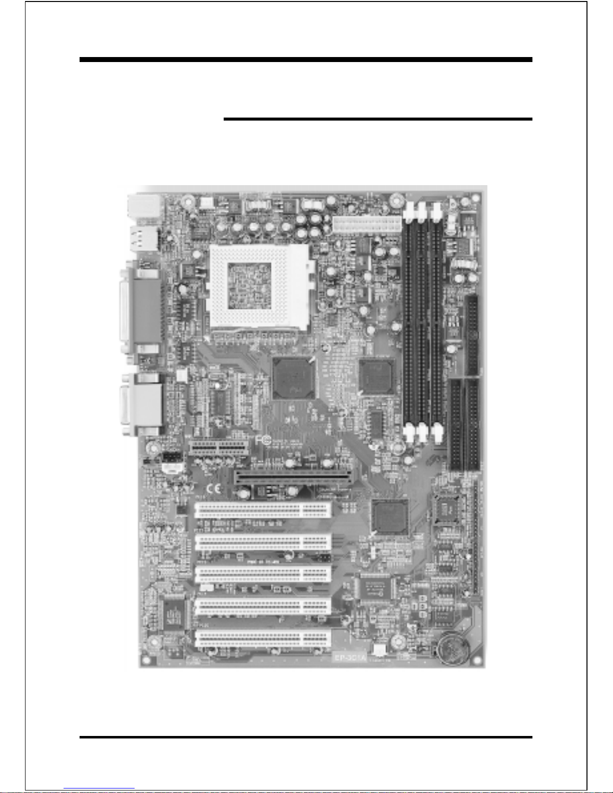
IntroductionEP-3C1A
Page 1-1
Section 1
INTRODUCTION
Components Checklist
üü
üü
ü A. (1) EP-3C1A mainboard
üü
üü
ü B. (1) EP-3C1A users manual
üü
üü
ü C. (1) Floppy ribbon cable
üü
üü
ü D. (1) ATA-66 Hard drive ribbon cable
E. (1) PS/2 to AT keyboard connector adapter (optional)
üü
üü
ü F. (1) Driver and Ultility
G. (1) Digital Audio (SPDIF IN/OUT) Module and an optical
fiber (TOSLINK-TOSLINK Cable and 3.5 plug) (optional)
USERS
MANUAL
EP-3C1A
B
A
E
F
or
C
D
G
Page 8

Introduction EP-3C1A
Page 1-2
System Overview
The EP-3C1A is designed with Intel® 820 chipset. The Intel® 820 chipset includes
MCH (FW82820), ICH (FW82801) and FWH (N82802AB) three chips. The
Intel® 820 chipset is the third generation desktop chipset designed for Intels FCPGA package architecture processor and the first chipset to support the 4X
capability of the AGP 2.0 Interface Specification. The MTH (82805AA) provides
the capability to support 100MHz SDRAMs on DIMMs socket. A new chipset
component interconnect, the hub interface, is designed into the Intel® 820 chipset
to provide more efficient communication between chipset components.
Support of AGP 4X, 100MHz SDRAM and the hub interface provides a balanced
system architecture for the Pentium® III or later socket 370 architecture processor minimizing bottlenecks and increasing system performance. By increasing
memory bandwidth to 1.6GB/s through the use of AGP 4X, the Intel® 820 chipset
will deliver the data throughput necessary to take advantage of the high performance provided by the powerful Pentium® III or later socket 370 architecture
processor.
The Intel® 820 chipset architecture removes the requirement for the ISA expansion bus that was traditionally integrated into the I/O subsystem of Intel chipsets.
This removes many of the conflicts experienced when installing hardware and
drivers into legacy ISA systems. The elimination of ISA will provide true plug-and
play for the Intel® 820 platform.
Intel® 820 chipset contains four core components: the Memory Controller Hub
(MCH), Memory Translator Hub (MTH), the I/O Controller Hub (ICH) and the
Firmware Hub (FWH). The MCH integrates the 133MHz, Pentium® II/III processor bus controller, AGP 2.0 controller, 100MHz SDRAM controller and a highspeed hub interface for communication with the ICH. The ICH integrates an
UltraATA/66 controller, USB host controller, LPC interface controller, FWH
interface controller, PCI interface controller, and a hub interface for communication with the MCH. The Intel® 820 chipset will provide the data buffering and
interface arbitration required to ensure that system interfaces operate efficiently
and provide the system bandwidth necessary to obtain peak performance the
Pentium® III or later socket 370 architecture.
Page 9

IntroductionEP-3C1A
Page 1-3
Chipset Components
The Intel® 820 chipset consists of the Memory Controller Hub (MCH), Memory
Translator Hub (MTH), the I/O Controller Hub (ICH) and the Firmware Hub (FWH).
ww
ww
w Memory Controller Hub (MCH)
The MCH provides the interconnect between the Direct RambusTM Channel and
the system logic. It integrates:
- Support for single Socket 370 processor with 100MHz or 133MHz System
Bus.
- 100MHz SDRAM interface supporting 768MB of SDRAM.
- 4X, 1.5V AGP interface (3.3V 1X, 2X and 1.5V 1X, 2X devices also
supported).
- Downstream hub link for access to the ICH.
ww
ww
w Memory Translator Hub (MTH)
The MTH provides the capability to support SDRAM memory on a Direct
RambusTM Channel.
- Support 100MHz SDRAMs on DIMMs
- 64Mbit and 128Mbit SDRAM technologies
- X4, X8 and X16 SDRAM components
- X4 Registered DIMMs
ww
ww
w I/O Controller Hub (ICH)
The I/O controller Hub provides the I/O subsystem with access to the rest of
the system. Additionally, it integrates may I/O functions. The ICH integrates:
- Upstream hub link for access to the MCH
- 2 Channel Ultra ATA/66 Bus Master IDE controller
- USB controller
- SMBus controller
Page 10

Introduction EP-3C1A
Page 1-4
- FWH interface
- LPC interface
- PCI 2.2 interface
- Integrated System Management Controller
ww
ww
w Firmware Hub (FWH)
The FWH component is a key element to enabling a new security and manageability infrastructure for the PC platform. The device operates under the FWH
interface and protocol. The hardware features of this device include a unique a
Random Number Generator (RNG), register-based locking, and hardwarebased locking.
Page 11

IntroductionEP-3C1A
Page 1-5
Overview
Intel Coppermine processors of Flip-chip pin grid
array (FC-PGA) Package
These Coppermine-128K and Coppermine-256K processor is the next addition to
the P6 micro architecture product family. The FC-PGA package is a new addition to
the Intel IA-32 processor line and hereafter will be referred to as the Coppermine
FC-PGA processor, or simply The processor. The package utilizes the same 370pin zero insertion force socket (PGA370) used by the Intel Celeron processor.
Thermal solutions are attached directly to the back of the processor core package
without the use of a thermal plate or heat spreader.
The Coppermine processor, like the Intel Celeron, Intel Pentium II and Pentium III
in the P6 family processor, implement a Dynamic Execution micro architecture --a unique combination of multiple branch prediction, data flow analysis, and speculative execution. This enable these processors to deliver higher performance than the
Intel Pentium processor, while maintaining binary compatibility with all previous
Intel Architecture processors. The processor also executes Intel MMX technology
instructions for enhanced media and communication performance just as its predecessor the Intel Pentium III processor. Additionally the Coppermine FC-PGA processor executes streaming SIMD (Single-Instruction Multiple Data) Extensions for
enhanced floating point and 3-D application performance. The concept of processor identification, via CPUID, is extended in the processor family with the addition
of a processor serial number. The processor utilizes multiple low-power states
such as AutoHALT, Stop-Grant, Sleep and Deep Sleep to conserve power during idle
times.
The processor includes an integrated on-die, 128KB or 256KB, 8-way set associative level-two (L2) cache with a separated 16KB level one (L1) instruction cache
and 16KB level one (L1) data cache. These cache arrays run at the full speed of the
processor core. As with the Intel Pentium III processor, the Coppermine FC-PGA
processor has a dedicated L2 cache bus, thus maintaining the dual independent bus
architecture to deliver high bus bandwidth and performance. Memory is cacheable
for 4GB/64GB of addressable memory space, allowing significant headroom for
desktop system.
Page 12
Introduction EP-3C1A
Page 1-6
Flip-chip pin grid array (FC-PGA) 370 processor
Installation and Removal
Installation:
Install the processor and the fan heatsink using the Installation Notes provided with
the boxed processor. The FC-PGA processor with package dimensions is provided
to aid in the design of heatsink and clip solutions as well as demonstrate where pin
side capacitors will be located on the processor. First, raise the handle of the 370pin socket. Carefully install the processor into the 370-pin socket making sure that
none of the pins are bent. Then close the handle of the socket. Next install the fan
heatsink. Make sure to install the heatsink onto the processor after the processor
has been inserted into the 370-pin socket. Place the fan heatsink onto the processor
such that the integrated clip lines up with the sockets attach tabs. This will align
the fan cable with the PGA370 mark on the 370-pin socket. Remember not to damage
the thermal interface pad. Attach
the clip onto the sockets attach
tabs. (A small tool, such as a pen,
may make this process easier.) Take
care to consider potential scraping
of the motherboard underneath the
370-pin socket attach tabs. Connect
the attached fan power cable to the
motherboard connector and quickly
power on the system to verify that
the processor fan is running.
Removal:
To simplify the following process, consider removing the motherboard from the chassis before removing the processor. First, unplug the fan power cable from the
motherboards connector. Then pull the integrated clip away from the sockets tab
nearest the fan cable. (A small tool, such as a pen or screwdriver, may make this
process easier.) Once the clip is free, slowly lift the fan heatsink straight up away
from the socket and the processor. (If the processor has been in operation for a long
Page 13

IntroductionEP-3C1A
Page 1-7
period of time, then this step may require some extra force; this is because the heat
dissipated from the processor will have affected the thermal interface pad) Next, lift up
the handle of the 370-pin socket. Finally, carefully remove the processor from the
socket making sure not to bend any of the processor pins.
Bandwidth Overview
Table 1 provides a summary of the bandwidth requirements for the Intel® 820 chipset.
Table 1: Intel® 820 platform Bandwidth Summary
ecafretnI
deepSkcolC
)zHM(
rePselpmaS
kcolC
etaRataD
)s/selpmas-ageM(
htdiWataD
)setyB(
htdiwdnaB
)s/BM(
suBUPC
3.331/00113.331/00186601/008
MARDS
0012 0082 008
0.2PGA
6.664 6624 6601
kniLbuH
6.664 6621 662
2.2ICP
3.331 3.334 331
Page 14

Introduction EP-3C1A
Page 1-8
Accelerated Graphics Port
(AGP or A.G.P.)
Typically, 3D graphics rendering requires a tremendous amount of memory, and
demands ever increasing throughput speed as well. As 3D products for the
personal computer become more and more popular, these demands will only
increase. This will cause a rise in costs for both end users and manufacturers.
Lowering these costs as well as improving performance is the primary motivation
behind AGP. By providing a massive increase in the bandwidth available between
the video card and the processor, it will assist in relieving some of these pressures
for quite sometime.
The EP-3C1A provides the AGP 2.0 interface. The AGP Interface Specification
revision 2.0 enhances the functionality of the original AGP Interface Specification (revision 1.0) by allowing 4X data transfers (4 data samples per clock) and 1.
5 volt (power supply) operation. The AGP 2.0 interface, along with Direct
Rambus memory technology, allows graphics controllers to access main memory
at over 1GB/s. In order to match the 1X, 2X and 4X AGP Card. The EP-3C1A
used the Universal AGP connector. To maximize add-in flexibility. (such as 1.5
volt for 1X, 2X and 4X or 3.3 volt for 1X and 2X AGP Card).
Ultra ATA/66
The ICH provides two channel Ultra ATA/66 Bus Master IDE controller, that
support Ultra ATA/66 protocols, perfect for such demanding applications as realtime video, multimedia, and high performance operating system. A new IDE cable
is required for Ultra ATA/66. This cable is an 80 conductor cable; however the
connectors are, of course, backwards compatible with ATA/33.
Hardware Monitoring
Hardware monitoring allows you to monitor various aspects of your systems
operations and status. The features include CPU temperature, voltage and RPM of
fan.
Page 15
IntroductionEP-3C1A
Page 1-9
EP-3C1A Form-Factor
The EP-3C1A is designed with ATX form factor - the latest industry standard of
chassis. The ATX form factor is essentially a Baby-AT baseboard rotated 90
degrees within the chassis enclosure and a new mounting configuration for the
power supply. With these changes the processor is relocated away from the
expansion slots, allowing them all to hold full length add-in cards. ATX defines
a double height aperture to the rear of the chassis which can be used to host a
wide range of onboard I/O. Only the size and position of this aperture is
defined, allowing PC manufacturers to add new I/O features (e.g.; TV input, TV
output, joystick, modem, LAN, audio, etc.) to systems. This will help systems
integrators differentiate their products in the marketplace, and better meet your
needs.
By integrating more I/O down onto the board and better positioning the
hard drive and floppy connectors material cost of cables and add-in cards is
reduced.
By reducing the number of cables and components in the system, manufac-
turing time and inventory holding costs are reduced and reliability will
increase.
By using an optimized power supply, it's possible to reduce cooling costs
and lower acoustical noise. An ATX power supply, which has a sidemounted fan, allows direct cooling of the processor and add-in cards
making a secondary fan or active heatsink unnecessary in most system
applications.
Full length
slots
Expandable I/O
Figure 3: Summary of ATX chassis features
CPU located near
Power Supply
Single chassis fan
for system
ATX power
connector
Floppy / IDE
connectors close to
peripheral bays
5 1/4"
Bay
3 1/2"
Bay
ATX
Power
Supply
Page 16
Introduction EP-3C1A
Page 1-10
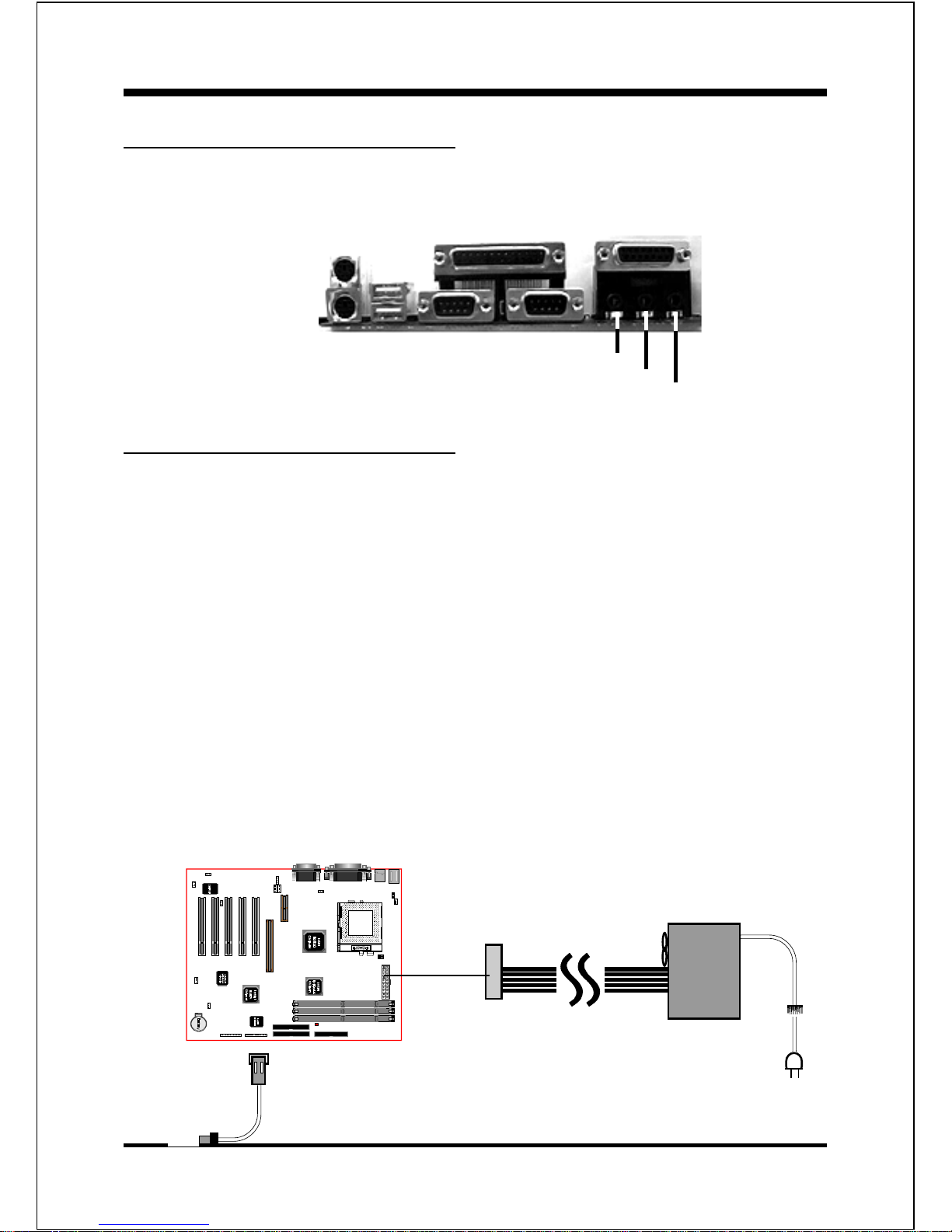
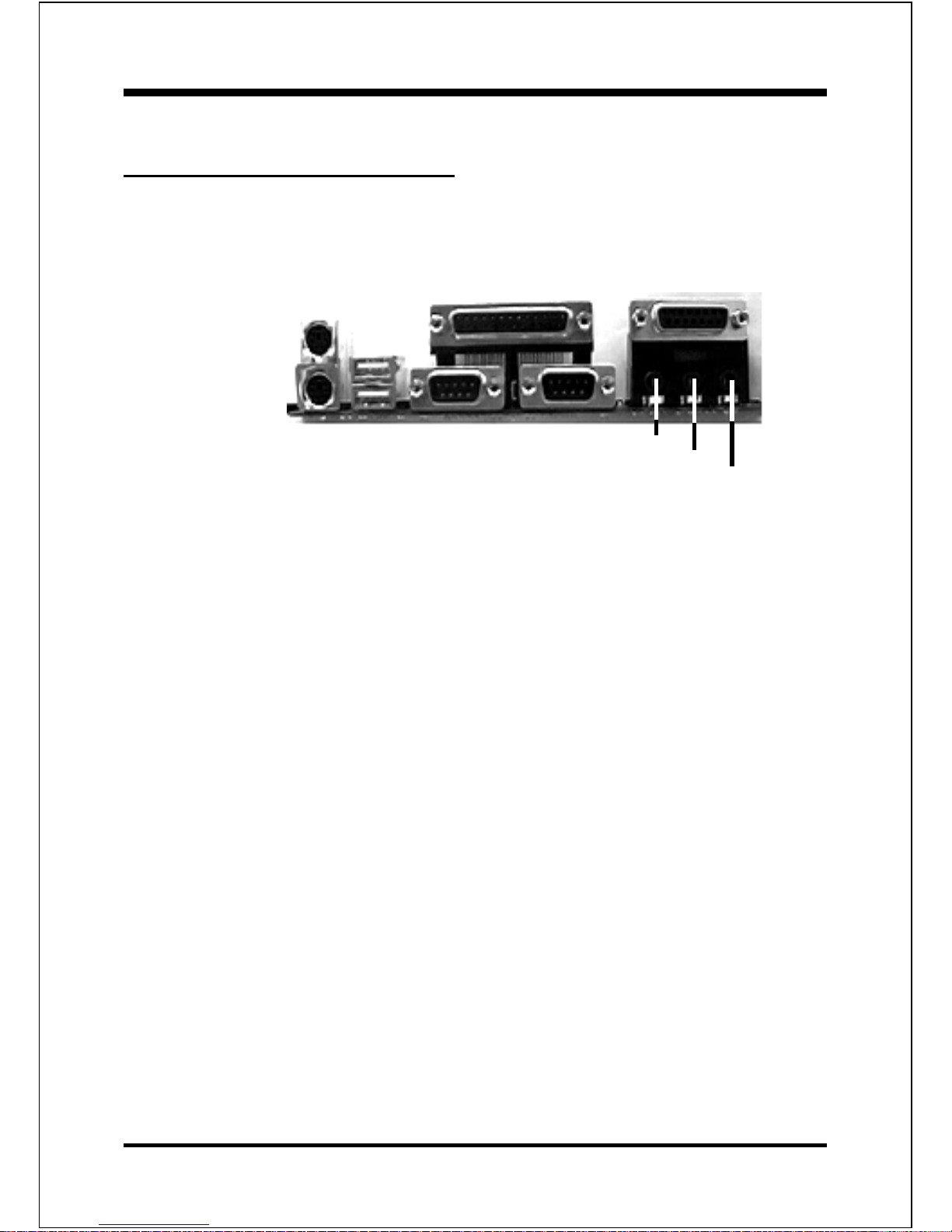
I/O Shield Connector
The EP-3C1A is equipped with an I/O back panel. Please use the appropriate I/O
shield (figure 4).
ATX
POWER SUPPLY
Power-On/Off (Remote)
The EP-3C1A has a single 20-pin connector for ATX power supplies. For ATX power
supplies that support the Remote On/Off feature, this should be connected to the
systems front panel for system Power On/Off button. The systems power On/Off
button should be a momentary button that is normally open.
The EP-3C1A has been designed with Soft Off" functions. You can turn Off the
system from one of two sources: The first is the front panel Power On/Off button,
and the other is the "Soft Off" function (coming from the EP-3C1As onboard circuit
controller) that can be controlled by the operating system. Windows 95/98 will
control this when the user clicks that they are ready to Shutdown the system.
Note: For maintaining the SDRAM power during STR (ACPI S3) function, it
is strongly recommend to use ATX power supplies that have a +5VSB
current of (>=) 1A (1000mA). Please check the 5VSBs specification
that has been printed on the ATX power supplys outer case.
Case (chassis) Power
ON/OFF button
Figure 5: Simple ATX Power
ON/OFF Controller
J3
Figure 4: I/O back panel layout
PS/2 Mouse
PS/2
KEYBOARD
USB port
COM1 COM2
parallel port
Speaker
Line_in
MIC
Joystic/Midi port
Page 17
IntroductionEP-3C1A
Page 1-11
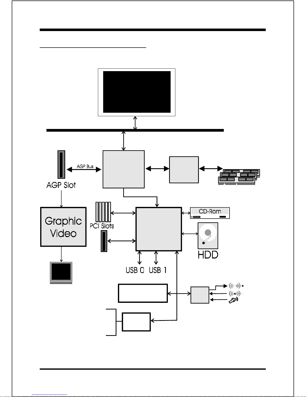
Figure 6: System Block Diagram
System Block Diagram
A Socket 370
Processor
MCH
(Memory
Controller
Hub)
MTH
(Memory
Translator
Hub)
ICH
(I/O
Controllrer
Hub)
100MHz
DIMM Modules
100/133MHz
66MHz
4X, 2X
AMR Slot
FWH (Firm Ware Hub)
Flash memory
LPC I/O
Winbond
83627HF
Serial Port 1
serial Port 2
LPT Port
PS/2 Mouse
PS/2 Keyboard
PCI
Sound
(100/133MHz FSB only)
Page 18

Introduction EP-3C1A
Page 1-12
Page Left Blank
Page 19

FeaturesEP-3C1A
Page 2-1
Section 2
FEA TURES
EP-3C1A Fea tures:
EP-3C1A is based on the Socket 370 Processors including FC- PGA operat-
ing at 500 ~ 733MHz (100MHz or 133MHz FSB only, dont supports 66MHz
processor). The board is configured by a BIOS setting to match your CPU
clock speed.
Designed with Intels 820 Chipset.
Supports up to 768MB of SDRAM (minimum of 64 MB) on board, You can use
168-pin DIMM x 3 to plug in the DIMM socket (please see Section 3-2).
EP-3C1A will not support ECC (Error Checking and Correction) mode.
Supports Universal AGP connector for 1X, 2X or 4X AGP Card.
Supports (5) 32 bit PCI slots, (1) AGP slot and provides (2) independent high
performance PCI IDE interfaces capable of supporting PIO Mode 3/4 and
Ultra DMA 33/66 devices. The EP-3C1A supports (5) PCI Bus Master slots
and a jumperless PCI INT# control scheme which reduces configuration
confusion when plugging in PCI card(s).
Supports ATAPI (e.g. CD-ROM) devices on both Primary and Secondary IDE
interfaces.
Designed with Winbond W83627HF LPC I/O: (1) floppy port, (1) parallel
port (EPP, ECP), and (2) serial ports (16550 Fast UART).
Note: Japanese Floppy 3 mode is also supported
Advanced Configuration Power Interface (ACPI) Ready.
Y2K Compliant.
Features Award Plug & Play BIOS. With Flash Memory you can always
upgrade to the current BIOS as they are released. (http://www.epox.com
please visit our Technical Support section for the latest updates).
EP-3C1A utilizes a Lithium battery which provides environmental protec-
tion and longer battery life.
Page 20

Features EP-3C1A
Page 2-2
Supports the Universal Serial Bus (USB) connector. The onboard ICH chip
provides the means for connecting PC peripherals such as; keyboards,
joysticks, telephones, and modems.
Built-in ATX 20-pin power supply connector.
Software power-down when using Windows® 95/98.
Supports ring-in feature (remote power-on through external modem, allows
system to be turned on remotely).
Resume by Alarm - Allows your system to turn on at a preselected time.
Supports CPU Hardware sleep and SMM (System Management Mode).
Supports Hot key, Any key or password Keyboard power ON function
(KBPO).
Supports USDM software to offer motherboard various status on Windows
®
95/98.
Supports the CPU, PWR and Chassis fan Auto stop in sleep mode.
Supports the onboard standby and blinks in suspend green or STR mode on
J2 (Power LED).
Supports the STR (Suspend To SDRAM) power management by ACPIs S3.
Supports the STR indicator red LED (D13) to avoid pluging or un-pluging
DIMM modules when in a STR mode.
Supports the System Power LED (PANEL) blinking in the sleep mode.
Built-in WOL (Wake On Lan) Connector.
Supports an AMR Connector for use with a software AMR modem card.
(AMR card is Primary only).
Built-in C-Media CMI8738 PCI Sound Onboard.
True Full Duplex playback and recording, built-in 16 bits CODEC.
HRTF 3D positional audio, supports both Direct Sound 3D® & A3D
®
interface, two and four channel speaker mode.
Supports OPL3, MPU401 UART mode and Joystick function.
Downloadable Wave Table Synthesizer, supports Direct Music®.
Supports Digital Audio (SPDIF IN/OUT) module (Optional).
Page 21
InstallationEP-3C1A
Page 3-1
Section 3
INSTALLATION
Page 22
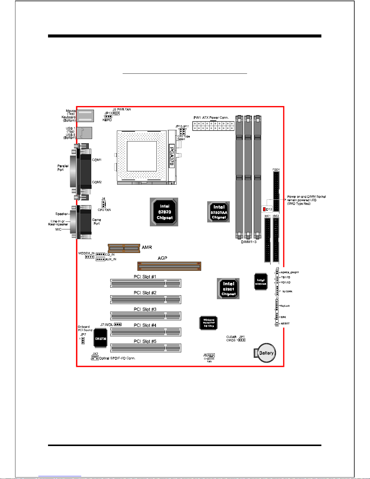
Installation EP-3C1A
Page 3-2
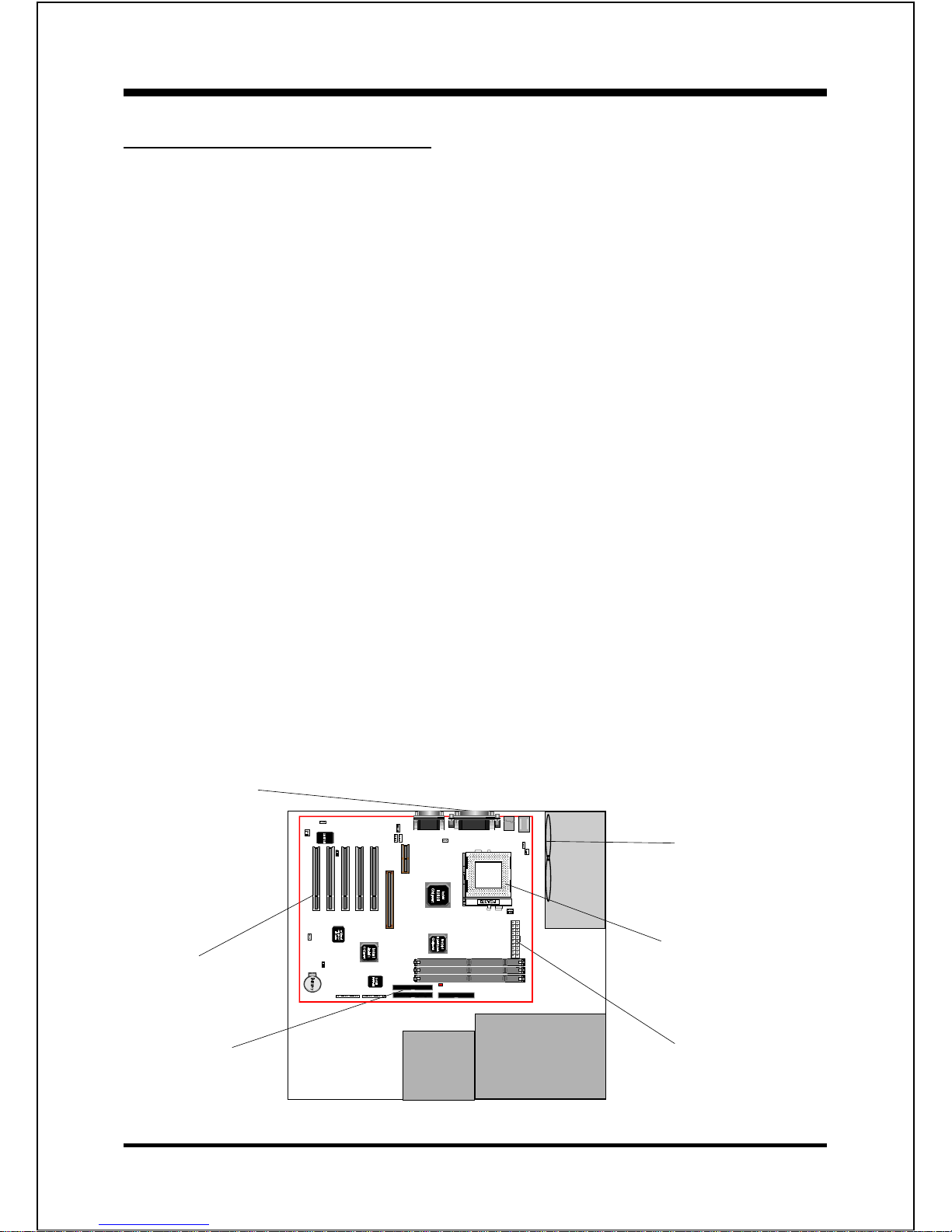
Figure 1
EP-3C1A Detailed Layout
Page 23

InstallationEP-3C1A
Page 3-3
Easy Installation Procedure
The EP-3C1A is designed for high speed 100MHz or 133MHz FSB Socket 370
processors only, such as Intel FC-PGA 370 CuMine (Coppermine) 128K/256K
processors which are based on 0.18 micro process technology and utilizing the
AGTL+ bus architecture at 100 and 133MHz.
The EP-3C1A has the very few jumpers on board, making your installation faster and
easier. In despite of user friendly design, the EP-3C1A offers the flexible FSB
selection, being capable of running speedy FSB at 133MHz for Intel PIII CuMine
CPU & upcoming new Cyrix Socket 370 processors.
Before you get started, please read the following quick installation guide with
careful.
Easy Installation Procedure
The following must be completed before powering on your new system:
3-1. CPU Insertion
3-2. Jumper Settings
3-3. System memory Configuration
3-4. Device Connectors
3-5 External Modem Ring-in Power ON and Keyboard Power ON
Functions (KBPO)
3-6. STR (Suspend To RAM) Function
Section 3-1
CPU Insertion
CPU Insertion: (use CuMineTM for reference)
Step 1
Open the socket by raising the actuation
lever.
Figure 2
Page 24
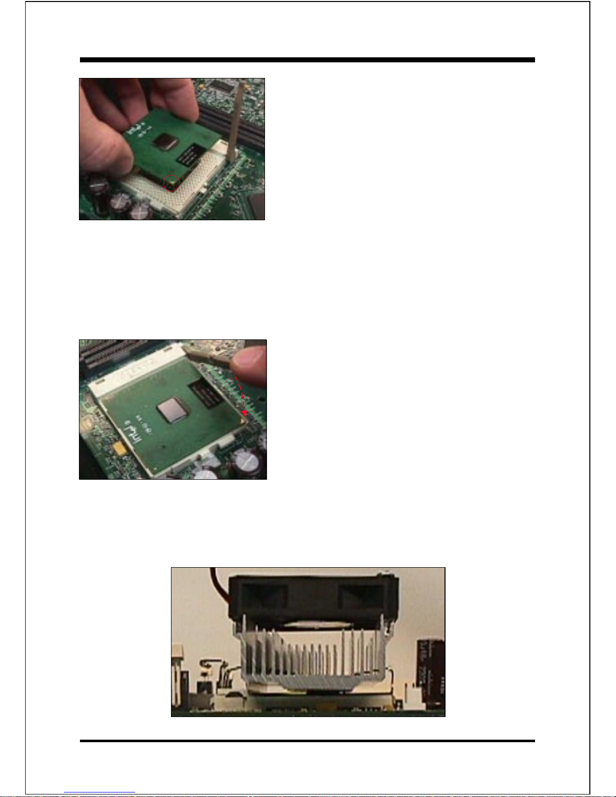
Installation EP-3C1A
Page 3-4
Step 2
Insert the processor.
Ensure proper pin 1 orientation by aligning
the FC-PGA corner marking with the socket
corner closest to the actuation arm tip. The
pin field is keyed to prevent mis-oriented
insertion.
Dont force processor into socket. If it does
not go in easily, check for mis-orientation and
debris.
Make sure the processor is fully inserted
into the socket on all sides.
Step 3
Close the socket by lowering and locking the
actuation lever.
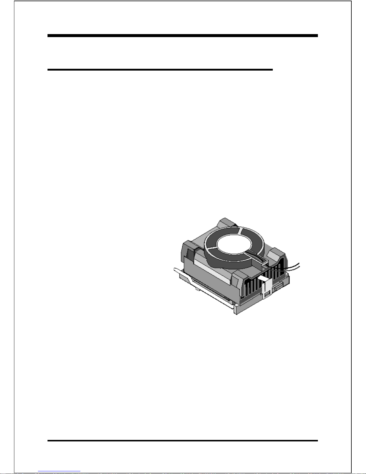
Note: Intels reference design thermal solution is an active heatsink; an extruded alumi-
num heatsink based and a fan attached to the top on the fin array. (See Figure 5)
Figure 3
Figure 4
Figure 5
Page 25

InstallationEP-3C1A
Page 3-5
Processor
Core Frequency
(MHz)
System Bus
Frequency
(MHz)
L2 Cache Size
(Kbytes)
L2 Cache Type CPUID
3
533EB
1
533 133 256 A TC
2
068xh
550E
1
550 100 256 A TC
2
068xh
600E
1
600 100 256 A TC
2
068xh
600EB
1
600 133 256 A TC
2
068xh
650E
1
650 100 256 A TC
2
068xh
667EB
1
667 133 256 A TC
2
068xh
700E
1
700 100 256 A TC
2
068xh
733EB
1
733 133 256 A TC
2
068xh
The table listing all Coppermine processor identification
Notes:
1. B -- 133MHz System Bus Frequency
E -- Processor with Advanced Transfer Cache (CPUID 068xh).
2. ATC = Advanced Transfer Cache. ATC is an L2 Cache integrated on the same
die as the processor core. With ATC, the interface between the processor core
and L2 Cache is 256-bits wide, runs at the same frequency as the processor core
and has enhanced buffering.
3. The Pentium® III Processor Specification Update for the exact CPUID for each
processor.
Page 26
Installation EP-3C1A
Page 3-6
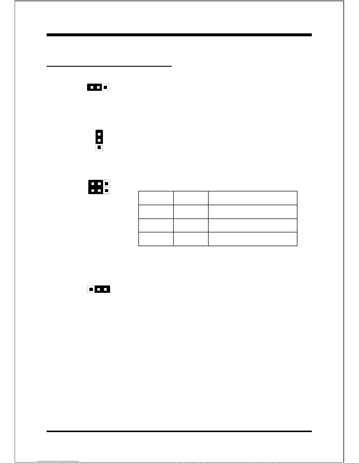
Section 3-2
Jumper Settings
1
JP1 CMOS Clear
JP1 = 1-2 Normal (Default)
= 2-3 Clear CMOS
1
1
JP10
JP11
CPU Type Select
1
JP7 On Board PCI Sound
JP7 = 1-2 Enabled PCI Sound (Default)
= 2-3 Disabled PCI Sound yrix CPU
JP13
Keyboard Power-ON Function
JP13= 1-2 Enabled
= 2-3 Disabled (Default)
1
01PJ11PJepyTUPC
2-1X )tluafeD(UPCletnI
3-23-2*sUPCrehtOzHM001
3-22-1*sUPCrehtOzHM331
X: Dont Care
* : Reserved
Page 27
InstallationEP-3C1A
Page 3-7
latoT
yromeM
1MMID
)1/0knaB(
)1/0swoR(
2MMID
)3/2knaB(
)3/2swoR(
3MMID
)2/3knaB(
)2/3swoR(
BM652=
mumixaM
*MARDS/ODE
,BM46,BM23,BM61,BM8
1xBM652,BM821
*)SSroSD(
enoNenoN
BM215=
mumixaM
*MARDS/ODE
,BM46,BM23,BM61,BM8
1xBM652,BM821
*)SSroSD(
*MARDS/ODE
,BM46,BM23,BM61,BM8
1xBM652,BM821
*)SSroSD(
enoN
BM867=
mumixaM
*MARDS/ODE
,BM46,BM23,BM61,BM8
1xBM652,BM821
*)SSroSD(
*MARDS/ODE
,BM46,BM23,BM61,BM8
1xBM652,BM821
*)ylnOSS(
*MARDS/ODE
,BM46,BM23,BM61,BM8
1xBM652,BM821
*)ylnOSS(
* SDRAM only supports 8, 16, 32, 64, 128, 256MB DIMM modules.
* Using non-compliant memory with higher bus speed (over clocking) may severely
compromise the integrity of the system.
* DS : Double Side Memory Module
* SS : Single Side Memory Module
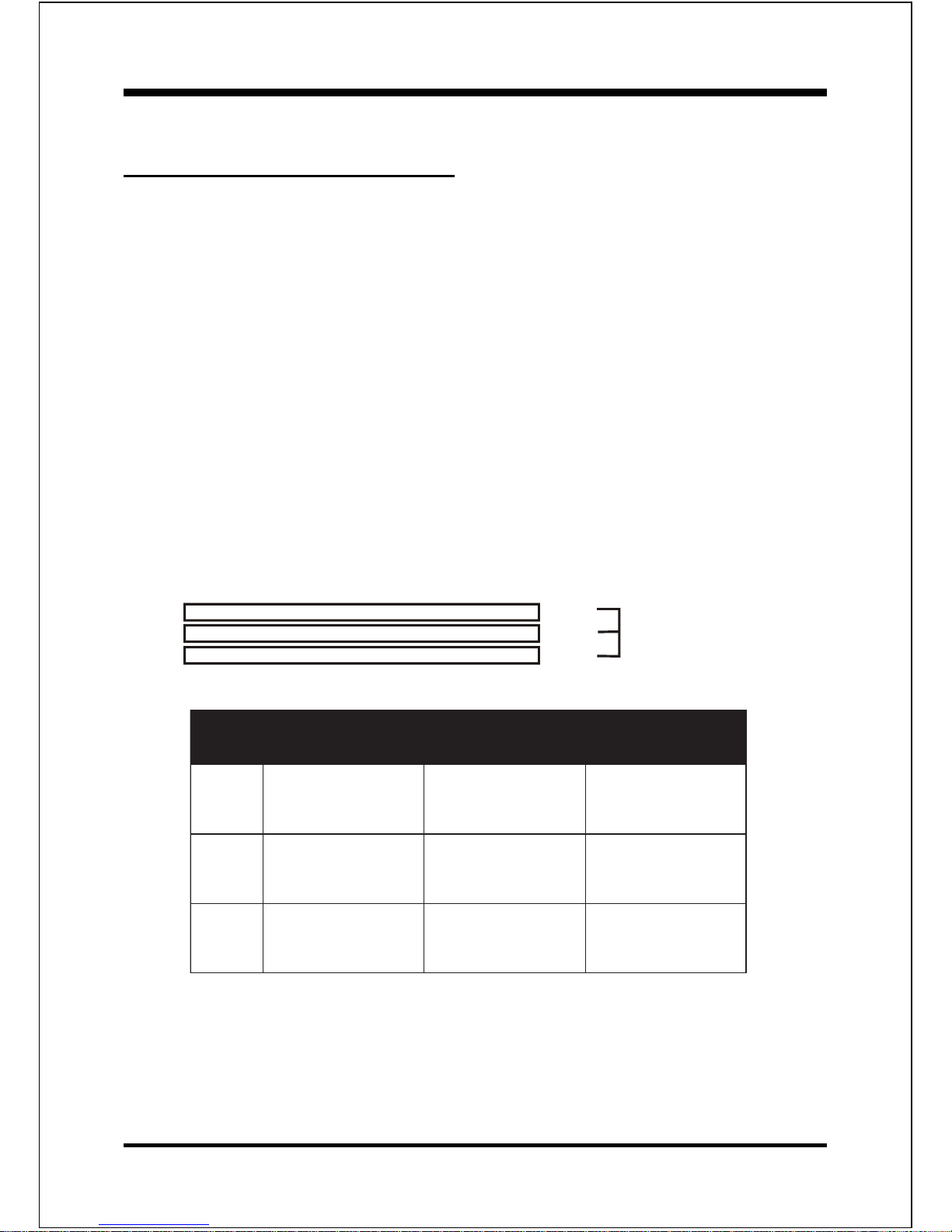
Section 3-3
System Memory Configuration
Memor y Layout
The EP-3C1A supports (3) 168-pin DIMMs (Dual In-line Memory Module). Sockets
are available for 3.3Volt (power level) Synchronous Dynamic Random Access
Memory (SDRAM) of 8, 16, 32, 64, 128MB or 256MB.
This board supports SPD DIMMs Modules only.
This board supports 64Mbit and 128Mbit SDRAM technologies.
The registered DIMM Supports 32Mx4 128Mbit Memory Modules only.
We recommend using at least 125MHz (-8ns) SDRAM DIMM at the 100MHz
(or higher) FSB as timing becomes more critical at these higher speeds.
DIMM SDRAM may be 83MHz (-12ns), 100MHz (-10ns) or 125MHz (-8ns)
bus speed.
Figure 6 and Table 1 show several possible memory configurations using
Figure 6
Table 1
DIMM 1 (M1)
DIMM 2 (M2)
DIMM 3 (M3)
Bank 0/1
Bank 2/3
Bank 3/2
-Synchronous
-SDRAM DIMM
Page 28
Installation EP-3C1A
Page 3-8
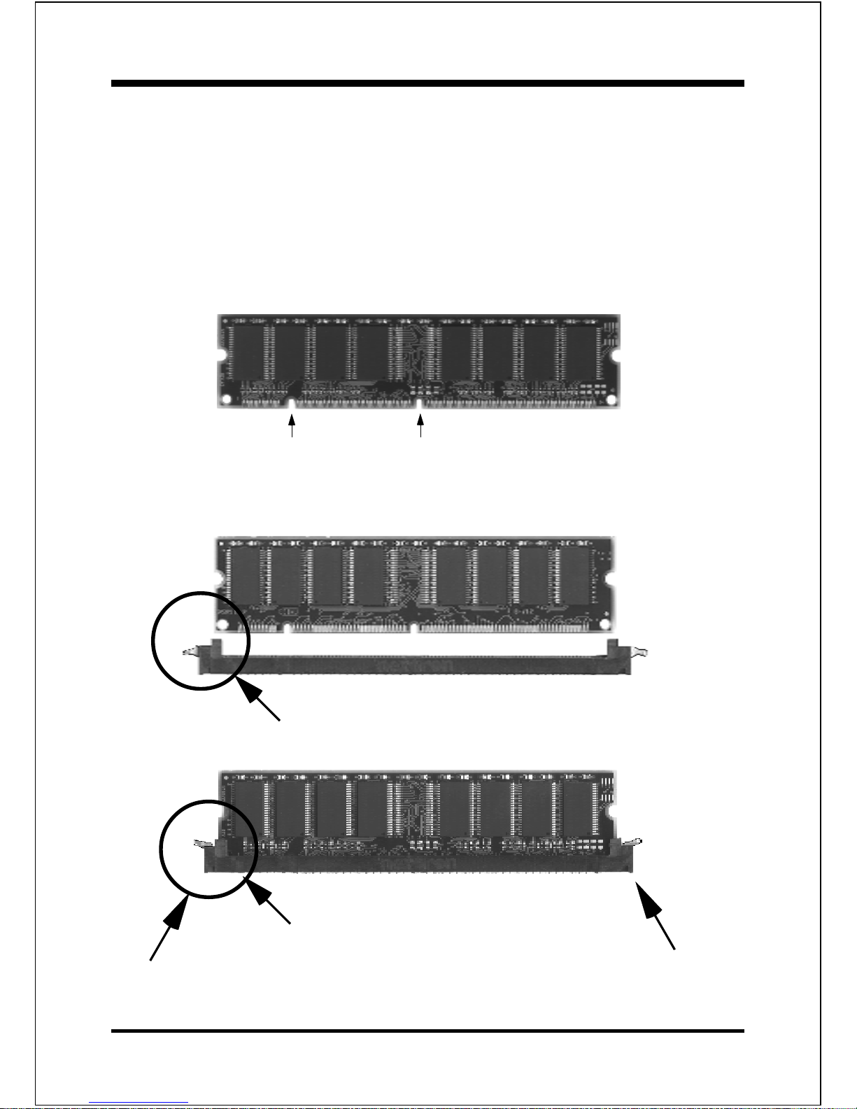
DIMM Module Installation
Figure 7 displays the notch marks and what they should look like on your DIMM
memory module.
DIMMs have 168-pins and two notches that will match with the onboard DIMM
socket. DIMM modules are installed by placing the chip firmly into the socket at
a 90 degree angle and pressing straight down (figure 8) until it fits tightly into the
DIMM socket (figure 9).
Figure 7
Figure 9
DIMM Module clip after installation
To remove the DIMM module simply press down both of the white clips on
either side and the module will be released from the socket.
Figure 8
DIMM Module clip before installation
CENTER KEY ZONE
(3.3 V DRAM)
LEFT KEY ZONE
(UNBUFFERED)
Page 29
InstallationEP-3C1A
Page 3-9
Section 3-4
Device Connectors
Please install the motherboard into the chassis.
Now that your motherboard is installed you are ready to connect all your connections (figure 10).
J2,J3: Chassis Panel Connector
Power LED, Keylock, Speaker, Reset, Sleep, Turbo LED and HDD LED
J4: CPU Fan Power
A plug-in for the CPU Fan Power
J5: Power Supply Fan Monitoring
A plug-in for the Power supply so that BIOS can monitor the RPMs
J6: Chassis Fan Power
A plug-in for the chassis Fan Power
J7: WOL (Wake On Lan) Connector
PW1: ATX Power Connector
20-pin power connector
IDE1: Primary IDE Connector
IDE2: Secondary IDE Connector
FDD1: Floppy Controller Connector
CD-IN: CD Audio_IN Connector
Pin1(CD_IN_Left), Pin2/Pin3(GND), Pin4(CD_IN_Right)
AUX_IN: Auxiliary Line_IN Connector
Pin1(Left Line_IN), Pin2/Pin3(GND), Pin4(Right Line-IN)
MODEM_IN: Telephony Connector
Pin1(Audio_in), Pin2/Pin3(GND), Pin4(Mic-out to Modem)
JX2: OPTICAL SPDIF-I/O
Figure 10
PS/2 Mouse
PS/2
KEYBOARD
USB port
COM1 COM2
parallel port
Speaker
Line_in
or
Rear speaker
MIC
Joystic/Midi port
Page 30
Installation EP-3C1A
Page 3-10
Device Connectors (continued)
(This is connected to the power button on the case. Using the Soft-Off
by Pwr-BTTN feature, you can choose either Instant Off (turns system
off immediatly), or 4 sec delay (you need to hold the button down for
4 seconds before the system turns off). When the system is in 4 sec
delay mode, there is a special feature to make the system to go into
suspend mode when the button is pressed momentarily.)
Turbo LED indicator - LED ON when higher speed is selected
IDE LED indicator - LED ON when Onboard PCI IDE Hard disks
is activate
J3
1
+
+
IR Connector
1. VCC 4. GND
2. NC 5. IRTX
3. IRRX
1
Power On/Off
J2
Speaker -
Connect to the system's speaker for beeping
1. Speaker 3. GND
2. N/C 4. GND
Reset - Closed to restart system.
KeyLock - Keyboard lock switch & Power LED connector
1. Power LED(+) 4. KeyLock
2. N/C 5. GND
3. GND
1
1
1
* The power LED lights when the system is
powered on and blinks in SLEEP MODE
(Suspend mode) and STR Mode.
Page 31

InstallationEP-3C1A
Page 3-11
Device Connectors (continued)
The EP-3C1A supports one AMR1 connector to provide a Modem Code (MC) or
an Audio/Modem Codec (AMC) configuration. Note the AMR1 connector
supports Modem Riser Card (MR), Modem Code (MC) or Audio/Modem Code
(AMC) as primary only.
AMR1 Connector
Page 32

Installation EP-3C1A
Page 3-12
Section 3-5
External Modem Ring-in Power
ON and Keyboard Power ON
Functions (KBPO)
On the basis of bounded functions in I/O chipset, the two serial ports are able to support
the External Modem Ring-in Power ON function. Once users connect the external
modem to COM1 or COM2, the EP-3C1A mainboard allows users to turn on their
system through the remote and host's dial-up control.
Exclusive Keyboard Power ON Function
To innovate a unique feature to benefit users, we devoted the easiest and most
convenient way to turn on your system based on the the ATX power supply.
How to work with it
Step 1: Please check that JP13 is at position 1-2 after you finished the system
installation.
Step 2: Push the momentary switch (J3 PW-ON) to turn on your system and then push
again and hold for more than 4 seconds to turn it off affter counting memory.
Step 3: You can enjoy the Keyboard Power ON function (KBPO) by pressing any 1
key, Hot key (Ctrl-F1, F2.....F12), Password (A maximum of 5 charac ters can
be entered.) and BUTTON only to turn on your system. Please refer to the BIOS
Integrated peripherals setup for detail (Page 4-23).The BIOS Default is
keyboard Hot key <Ctrl> - <F1> to turn on the system. Your system will be
turned on automatically, after releasing the keys. To power off you system,
you can use the Soft-OFF function under Windows 95/98.
Notes:
1. Intel ATX version 2.01 specification has recommended you use the power supply
with 1.0A in 5.0VSB. With our EP-3C1A mainboard, the 5.0VSB standby power
only has to be > = 1A (1000mA) then you can enjoy this function.
JP13
Keyboard Power-ON Function
JP13= 1-2 Enabled
= 2-3 Disabled (Default)
1
Page 33

InstallationEP-3C1A
Page 3-13
3-6 STR (Suspend To RAM) Function
The EP-3C1A supports the STR power management state by maintaining the
appropriate states on the SDRAM interface signals. The power source must be
kept alive to the SDRAM during STR (ACPI S3). Advanced Configuration
Power Interface (ACPI) provides more Energy Saving Features for operating
systems that support OS such as Instant ON and QuickStartTM function.
1. To enable the ACPI function and use the STR functionally to save your system
energy, you are recommended to confirm the following requirements:
a. Please make sure the VGA card in your system is ACPI fully supported.
Some VGA cards or drivers do not provide ACPI function. It is suggested
you contact with VGA card vendors to get the right information and
technical support.
b. In BIOS, please select ACPI function: Enable and ACPI Suspend Type:
S3(STR) in the Power Management Setup menu.
c. Then, please type the following before installing the Windows® 98:
{Drive}:> Setup /p j
If Windows® 98 was installed in your system without the parameters above,
please do refer to your software manual or contact Microsoft for more
details on how to upgrade to ACPI support.
d. Restart your system and install VGA card driver properly.
e. Go in to the Advanced section of the Power Management icon of Control
Panel, and select Stand By in the Power Buttons.
2. To start the STR mode, please click the START button and choose Shut Down
icon. Then, select the Stand By option in the Shut Down Windows box to let
system go to STR mode. In the mean time, the onboard STR indicator - J2 Power
LED begins to 1Hz blinking to show your system is under STR mode.
Here are the differences between STR power saving mode and Green (or
Suspend) mode:
a. It is the most advanced Power Management mode
b. It cuts all the power supplied to peripherals except to Memory - max. power
saving
Page 34

Installation EP-3C1A
Page 3-14
ACPI Onboards LED Status Indicator Table
Status
Onboards
LED
Location
Plug in the ATX
Power Core
Power ON
J3(PW-ON)
Green Mode
(S1)
STR
(S3)
Shutdown
(Soft-OFF)
(S5)
D13
(Red LED)
ON ON ON ON OFF
J2
PW_LED
OFF ON 1/4Hz Blinking 1Hz Blinking OFF
c. It saves and keeps all on-screen data including any executed applications to
SDRAM.
d. You must push the Power button connected with onboard J3 pin to wake up
you system (not to click to mouse or press keyboard to wake up the system.)
Just pushing Power button, your system will quickly back to the last screen for you.
The LED Indicator for ACPI Status table shown below will guide you and give
you a reference for ACPI status on this mainboard.
Page 35

BIOSEP-3C1A
Page 4-1
Main Menu
Once you enter the AwardBIOS CMOS Setup Utility, the Main Menu will appear
on the screen. The Main Menu allows you to select from several setup functions and
two exit choices. Use the arrow keys to select among the items and press <Enter>
to accept and enter the sub-menu.
Note that a brief description of each highlighted selection appears at the bottom of
the screen.
Setup Items
The main menu includes the following main setup categories. Recall that some
systems may not include all entries.
Standard CMOS Features
Use this menu for basic system configuration.
Section 4
BIOS SETUP
Page 36

BIOS EP-3C1A
Page 4-2
Advanced BIOS Features
Use this menu to set the Advanced Features available on your system.
Advanced Chipset Features
Use this menu to change the values in the chipset registers and optimize your
systems performance.
Integrated Peripherals
Use this menu to specify your settings for integrated peripherals.
Power Management Setup
Use this menu to specify your settings for power management.
PnP / PCI Configuration
This entry appears if your system supports PnP / PCI.
PC Health Status
This item is only show the system health status (include Voltage, Fan speed, CPU
temperature...)
Frequency/Voltage Control
Use this menu to specify your settings for frequency/voltage control.
Load Fail-Safe Defaults
Use this menu to load the BIOS default values for the minimal/stable performance for your system to operate.
Load Optimized Defaults
Use this menu to load the BIOS default values that are factory settings for optimal performance system operations. While Award has designed the custom BIOS
to maximize performance, the factory has the right to change these defaults to
meet their needs.
Supervisor / User Password
Use this menu to set User and Supervisor Passwords.
Save & Exit Setup
Save CMOS value changes to CMOS and exit setup.
Exit Without Save
Abandon all CMOS value changes and exit setup.
Page 37

BIOSEP-3C1A
Page 4-3
4-1 Standard CMOS Setup
The items in Standard CMOS Setup Menu are divided into 10 categories. Each category includes no, one or more than one setup items. Use the arrow keys to highlight the item and then use the <PgUp> or <PgDn> keys to select the value you want
in each item.
Figure 1: The Main Menu
Page 38

BIOS EP-3C1A
Page 4-4
Item Options Description
Date Month DD YYYY Set the system date. Note that
the Day automatically hanges
when you set the date
Time HH : MM : SS Set the system time
IDE Primary Master
Options are in its sub menu
(described in Table 3)
Press <Enter> to enter the sub
menu of detailed options
IDE Primary Slave
Options are in its sub menu
(described in Table 3)
Press <Enter> to enter the sub
menu of detailed options
IDE Secondary Master
Options are in its sub menu
(described in Table 3)
Press <Enter> to enter the sub
menu of detailed options
IDE Secondary Slave
Options are in its sub menu
(described in Table 3)
Press <Enter> to enter the sub
menu of detailed options
Drive A
Drive B
None
360K, 5.25 in
1.2M, 5.25 in
720K, 3.5 in
1.44M, 3.5 in
2.88M, 3.5 in
Select the type of floppy disk
drive installed in your system
Video
EGA/VGA
CGA 40
CGA 80
MONO
Select the default video device
Halt On
All Errors
No Errors
All, but Keyboard
All, but Diskette
All, but Disk/Key
Select the situation in which
you want the BIOS to stop the
POST process and notify you
Base Memory N/A
Displays the amount of
conventional memory detected
during boot up
Extended Memory
N/A
Displays the amount of
extended memory detected
during boot up
Total Memory N/A
Displays the total memory
available in the system
Main Menu Selections
This table shows the selections that you can make on the Main Menu
Table 2 Main Menu Selections
Page 39

BIOSEP-3C1A
Page 4-5
IDE Adapters
The IDE adapters control the hard disk drive. Use a separate sub menu to configure
each hard disk drive.
Figure 2 shows the IDE primary master sub menu.
Figure 2 IDE Primary Master sub menu
Page 40

BIOS EP-3C1A
Page 4-6
Use the legend keys to navigate through this menu and exit to the main menu. Use
Table 3 to configure the hard disk.
Item Options Description
IIDE HDD Auto-detection Press Enter Press Enter to auto-detect the HDD
on this channel. If detection is
successful, it fills the remaining
fields on this menu.
IDE Primary Master None
Auto
Manual
Selecting manual lets you set the
remaining fields on this screen.
Selects the type of fixed disk. "User
Type" will let you select the number
of cylinders, heads, etc.
Note: PRECOMP=65535 means
NONE !
Capacity Auto Display your disk
drive size
Disk drive capacity
(Approximated). Note that this
size is usually slightly greater than
the size of a formatted disk given by
a disk checking program.
Access Mode Normal
LBA
Large
Auto
Choose the access mode for this
hard disk
The following options are selectable only if the IDE Primary Master item is set to Manual
Cylinder Min = 0
Max = 65535
Set the number of cylinders for this
hard disk.
Head Min = 0
Max = 255
Set the number of read/write heads
Precomp Min = 0
Max = 65535
****
Warning
: Setting a value of
65535 means no hard disk
Landing zone Min = 0
Max = 65535
****
Sector Min = 0
Max = 255
Number of sectors per track
Table 1 Hard disk selections
Page 41

BIOSEP-3C1A
Page 4-7
4-2 Advanced BIOS Fea tures
This section allows you to configure your system for basic operation. You have the
opportunity to select the systems default speed, boot-up sequence, keyboard
operation, shadowing and security.
Virus Warning
Allows you to choose the VIRUS Warning feature for IDE Hard Disk boot sector
protection. If this function is enabled and someone attempt to write data into this
area, BIOS will show a warning message on screen and alarm beep.
Enabled: Activates automatically when the system boots up causing a warning
message to appear when anything attempts to access the boot sector
or hard disk partition table.
Disabled: No warning message will appear when anything attempts to access the
boot sector or hard disk partition table.
CPU Internal Cache/External Cache
These two categories speed up memory access. However, it depends on CPU/chipset
design.
Enabled: Enable cache
Disabled: Disable cache
Page 42

BIOS EP-3C1A
Page 4-8
CPU L2 Cache ECC Checking
This item allows you to enable/disable CPU L2 Cache ECC checking.
The choice: Enabled, Disabled.
Processor Number Feature
Pentium III or later CPU new feature. The default is Enabled.
Enabled: Processor serial number readable.
Disabled: Processor serial number disabled.
Quick Power On Self Test
This category speeds up Power On Self Test (POST) after you power up the computer.
If it is set to Enable, BIOS will shorten or skip some check items during POST.
Enabled: Enable quick POST
Disabled: Normal POST
First/Second/Third/Other Boot Device
The BIOS attempts to load the operating system from the devices in the sequence
selected in these items.
The Choice: Floppy, LS/ZIP, HDD, SCSI, CDROM, Disabled.
Swap Floppy Drive
If the system has two floppy drives, you can swap the logical drive name assignments.
The choice: Enabled/Disabled.
Boot Up Floppy Seek
Seeks disk drives during boot up. Disabling speeds boot up.
The choice: Enabled/Disabled.
Boot Up NumLock Status
Select power on state for NumLock.
The choice: On/Off.
Gate A20 Option
Select if chipset or keyboard controller should control GateA20.
Normal: A pin in the keyboard controller controls GateA20
Fast: Lets chipset control GateA20
Page 43

BIOSEP-3C1A
Page 4-9
Typematic Rate Setting
Key strokes repeat at a rate determined by the keyboard controller. When enabled, the
typematic rate and typematic delay can be selected.
The choice: Enabled/Disabled.
Typematic Rate (Chars/Sec)
Sets the number of times a second to repeat a key stroke when you hold the key down.
The choice: 6, 8, 10, 12, 15, 20, 24, 30.
Typematic Delay (Msec)
Sets the delay time after the key is held down before it begins to repeat the keystroke.
The choice: 250, 500, 750, 1000.
Security Option
Select whether the password is required every time the system boots or only when
you enter setup.
System The system will not boot and access to Setup will be denied if the
correct password is not entered at the prompt.
Setup The system will boot, but access to Setup will be denied if the
correct password is not entered at the prompt.
Note: To disable security, select PASSWORD SETTING at Main Menu and
then you will be asked to enter password. Do not type anything and
just press <Enter>, it will disable security. Once the security is
disabled, the system will boot and you can enter Setup freely.
OS Select For DRAM > 64MB
Select the operating system that is running with greater than 64MB of RAM on the
system. The choice: Non-OS2, OS2.
Report No FDD For Win 95
Whether report no FDD for Win 95 or not.
The choice: Yes, No.
Page 44

BIOS EP-3C1A
Page 4-10
4-3 Advanced Chipset Fea tures
This section allows you to configure the system based on the specific features of
the installed chipset. This chipset manages bus speeds and access to system memory
resources, such as DRAM and the external cache. It also coordinates communications between the conventional ISA bus and the PCI bus. It must be stated that these
items should never need to be altered. The default settings have been chosen because they provide the best operating conditions for your system. The only time you
might consider making any changes would be if you discovered that data was being
lost while using your system.
DRAM Settings (This field is no function)
The first chipset settings deal with CPU access to dynamic random access memory
(DRAM). The default timings have been carefully chosen and should only be altered
if data is being lost. Such a scenario might well occur if your system had mixed
speed DRAM chips installed so that greater delays may be required to preserve the
integrity of the data held in the slower memory chips.
Page 45

BIOSEP-3C1A
Page 4-11
SDRAM CAS Latency Time (This field is no function)
When synchronous DRAM is installed, the number of clock cycles of CAS latency
depends on the DRAM timing.
The Choice: Auto, 2, 3
SDRAM Buffer Strength
Selecting the SDRAMs MA, MD, CS Buffer Strength.le
The Choice: 1, 2, 3, Auto
System BIOS Cacheable
Selecting Enabled allows caching of the system BIOS ROM at F0000h-FFFFFh,
resulting in better system performance. However, if any program writes to this
memory area, a system error may result.
The choice: Enabled, Disabled.
Video BIOS Cacheable
Select Enabled allows caching of the video BIOS , resulting in better system
performance. However, if any program writes to this memory area, a system error
may result.
The Choice: Enabled, Disabled.
Video RAM Cacheable
This option allows the CPU to cache read/writes of the video RAM. The default is
Disabled.
Enabled: This option allows for faster video access.
Disabled: Reduced video performance.
Memory Hole At 15M-16M
You can reserve this area of system memory for ISA adapter ROM. When this area
is reserved, it cannot be cached. The user information of peripherals that need to use
this area of system memory usually discusses their memory requirements.
The Choice: Enabled, Disabled.
Delay Transaction
The chipset has an embedded 32-bit posted write buffer to support delay transactions cycles. Select Enabled to support compliance with PCI specification
version 2.1.
The Choice: Enabled, Disabled.
Page 46

BIOS EP-3C1A
Page 4-12
AGP Fast Write
Selecting Enabled allows to use Fast Write Protocol for 4X AGP.
The choice: Enbaled, Disabled.
AGP Aperture Size (MB)
The amount of system memory that the AGP card is allowed to share. The default
is 64.
4: 4MB of systems memory accessable by the AGP card.
8: 8MB of systems memory accessable by the AGP card.
16: 16MB of systems memory accessable by the AGP card.
32: 32MB of systems memory accessable by the AGP card.
64: 64MB of systems memory accessable by the AGP card.
128: 128MB of systems memory accessable by the AGP card.
256: 256MB of systems memory accessable by the AGP card.
Memory Parity Check
If the DRAM chip in your system support parity check, select Enabled.
Page 47

BIOSEP-3C1A
Page 4-13
OnChip Primary/Secondary PCI IDE
The integrated peripheral controller contains an IDE interface with support for two
IDE channels. Select Enabled to activate each channel separately.
The choice: Enabled, Disabled.
IDE Primary/Secondary Master/Slave PIO
The four IDE PIO (Programmed Input/Output) fields let you set a PIO mode (0-4)
for each of the four IDE devices that the onboard IDE interface supports. Modes 0
through 4 provide successively increased performance. In Auto mode, the system
automatically determines the best mode for each device.
The choice: Auto, Mode 0, Mode 1, Mode 2, Mode 3, Mode 4.
IDE Primary/Secondary Master/Slave UDMA
Ultra DMA/33 implementation is possible only if your IDE hard drive supports it
and the operating environment includes a DMA driver (Windows 95 OSR2 or a thirdparty IDE bus master driver). If your hard drive and your system software both support Ultra DMA/33, select Auto to enable BIOS support.
The Choice: Auto, Disabled.
4-4 Integrated Peripherals
Page 48

BIOS EP-3C1A
Page 4-14
USB Controller
Select Enabled if your system contains a Universal Serial Bus (USB) controller and
you have USB peripherals.
The choice: Enabled, Disabled.
USB Legacy Device Support
Select Enabled if your system contains a Universal Serial Bus (USB) controller and
you have a USB Legacy Device (Keyboard, Mouse).
The choice: Enabled, Disabled.
Init Display First
This item allows you to decide to active whether PCI Slot or on-chip VGA first
The choice: PCI Slot, Onboard .
AC97 Modem
This item allows you to decide to enable/disable the ICH chipset family to support
AC97 Modem.
Select Enable of AC97 Modem item, you must be primary Modem Riser Card
(MR) in hardware.
The choice: Enabled, Disabled.
IDE HDD Block Mode
Block mode is also called block transfer, multiple commands, or multiple sector
read/write. If your IDE hard drive supports block mode (most new drives do), select
Enabled for automatic detection of the optimal number of block read/writes per
sector the drive can support.
The choice: Enabled, Disabled
Power On Function
There are Button Only, Hot Key and Any key can be chosen by this field that
allows users to select one of these various functions as Power On Method for their
requirement. The default value in this selection is Hot Key. (Ctrl-F1)
Hot Key: User can press Control Key (Ctrl) and Function Key (from F1
to F12) individually to power on the system. The interval between
Ctrl key and function Key (F1-F12)must be short.
Anykey: Press anykey to power on the system.
Button Only: This power on function controlled by J3 (pw-on.) Use Power On
Button to power on the system.
Page 49

BIOSEP-3C1A
Page 4-15
Password: User can Power On the System by password, the password can be
entered from 1 to 5 characters. The maximum of password is 5
characters. If user forget / lost the password, please turn off the
system and open case to clear CMOS by JP1 to re-setting the
power on function. When set the password to turn on the system,
than cant power on by J3(PW-ON).
KB Power On Password
When the option of Power On Function is password selected, user uses the item to
key in password.
Hot Key Power On
Use this option with the above Power On Function to set a combination of keys
that can be used to power the system on. The default is Ctrl-F1.
Options: Ctrl-F1, Ctrl-F2, Ctrl-F3, Ctrl-F4, Ctrl-F5, Ctrl-F6, Ctrl-F7, Ctrl-F8, Ctrl-
F9, Ctrl-F10, Ctrl-F11, and Ctrl-F12.
Onboard FDC Controller
Select Enabled if your system has a floppy disk controller (FDC) installed on the
system board and you wish to use it. If you install and-in FDC or the system has no
floppy drive, select Disabled in this field.
The choice: Enabled, Disabled.
Onboard Serial Port 1/Port 2
Select an address and corresponding interrupt for the first and second serial ports.
The choice: 3F8/IRQ4, 2E8/IRQ3, 3E8/IRQ4, 2F8/IRQ3, Disabled, Auto.
UART Mode Select
This filed allows the users to configure what IR mode the 2nd serial port should use.
The default is Normal.
Optional: Normal, IrDA and ASKIR.
RxD, TxD Active
This field configures the receive and transmit signals generated from the IR port.
The default is Hi Lo (when UART Mode Select is not set to Normal).
Options: Hi Hi, Hi Lo, Lo Hi, and Lo Lo.
IR Transmission delay
The default is Enabled (when UART Mode Select is not set to Normal).
Options: Enabled and Disabled.
Page 50

BIOS EP-3C1A
Page 4-16
Onboard Parallel port
This field allows the user to configure the LPT port.
The default is 378H / IRQ7.
378H: Enable Onboard LPT port and address is 378H and IRQ7.
278H: Enable Onboard LPT port and address is 278H and IRQ5.
3BCH: Enable Onboard LPT port and address is 3BCH and IRQ7.
Disabled: Disable Onboard LPT port.
Parallel Port Mode
This field allows the user to select the parallel port mode.
The default is ECP+EPP.
Normal: Standard mode. IBM PC/AT Compatible bidirectional parallel port.
EPP: Enhanced Parallel Port mode.
ECP: Extended Capabilities Port mode.
EPP+ECP: ECP Mode & EPP Mode.
EPP Mode Select
This item allows you to determine the IR transfer mode of onboard I/O chip.
options: EPP1.9, EPP1.7.
ECP Mode USE DMA
This field allows the user to select DMA1 or DMA3 for the ECP mode.
The default is DMA3.
DMA1: This field selects the routing of DMA1 for the ECP mode.
DMA3: This field selects the routing of DMA3 for the ECP mode.
PWRON After PW-Fail
The system will stay of or power on after a power interrupte.
The default is OFF.
Fomer-Status: Stay off or power on depend on system safe shut-down or
power fail.
ON: System always power on after a power interrupte.
OFF: System always stay off after a power interrupte.
Page 51

BIOSEP-3C1A
Page 4-17
4-5 Po wer Management Setup
The Power Management Setup allows you to configure you system to most effectively save energy while operating in a manner consistent with your own style of
computer use.
ACPI Function
This item allows you to enable/disable the Advanced Configuration and Power Management (ACPI).
The choice: Enabled, Disabled.
ACPI Suspend Type
This item allows you to select S1(POS) or S3(STR) function.
The choice: S1(POS), S3(STR).
Power Management
This category allows you to select the type (or degree) of power saving and is directly related to the following modes:
1. HDD Power Down
2. Doze Mode
3. Suspend Mode
Page 52

BIOS EP-3C1A
Page 4-18
There are four selections for Power Management, three of which have fixed mode
settings.
Disable (default) No power management. Disables all four modes
Min. Power Saving Minimum power management. Doze Mode = 1
hr. Standby Mode = 1 hr., Suspend Mode = 1 hr.,
and HDD Power Down = 15 min.
Max. Power Saving
Maximum power management --
ONLY
AVAILABLE FOR SL CPUs
. Doze Mode = 1
min., Standby Mode = 1 min., Suspend Mode = 1
min., and HDD Power Down = 1 min.
User Defined Allows you to set each mode individually. When
not disabled, each of the ranges are from 1 min. to
1 hr. except for HDD Power Down which ranges
from 1 min. to 15 min. and disable.
Video Off Method
This determines the manner in which the monitor is blanked.
V/H SYNC+Blank This selection will cause the system to turn off the
vertical and horizontal synchronization ports and
write blanks to the video buffer.
Blank Screen This option only writes blanks to the video buffer.
DPMS Initial display power management signaling.
Video Off In Suspend
This determines the manner in which the monitor is blanked.
The choice: Yes, No.
Suspend Type
Select the Suspend Type.
The choice: PWRON Suspend, Stop Grant.
MODEM Use IRQ
This determines the IRQ in which the MODEM can use.
The choice: 3, 4, 5, 7, 9, 10, 11, NA.
Suspend Mode
When enabled and after the set time of system inactivity, all devices except the CPU
will be shut off.
The choice: Enabled, Disabled.
Page 53

BIOSEP-3C1A
Page 4-19
HDD Power Down
When enabled and after the set time of system inactivity, the hard disk drive will be
powered down while all other devices remain active.
The choice: Enabled, Disabled.
Soft-Off by PWR-BTTN
Pressing the power button for more than 4 seconds forces the system to enter the
Soft-Off state when the system has hung. The default is Instant-off.
The choice: Delay 4 Sec, Instant-Off.
PowerOn By Ring
This option is used to set the remote ring in and Wake on LAN (WOL) features.
The choice: Enabled, Disabled.
CPU THRM-Throttling
Select the CPU THRM-Throttling rate.
The choice: 25.0%, 37.5%, 50.0%, 62.5%, 75.0%, 87.5%.
** PM Events **
PM events are I/O events whose occurrence can prevent the system from entering a
power saving mode or can awaken the system from such a mode. In effect, the
system remains alert for anything which occurs to a device which is configured as
Enabled , even when the system is in a power down mode.
Primary IDE 0
Primary IDE 1
Secondary IDE 0
Secondary IDE 1
FDD, COM, LPT Port
PCI PIRQ[A-D] #
Page 54

BIOS EP-3C1A
Page 4-20
4-6 PnP/PCI Configuration Setup
This section describes configuring the PCI bus system. PCI, or Personal Computer
Interconnect, is a system which allows I/O devices to operate at speeds nearing the
speed the CPU itself uses when communicating with its own special components.
This section covers some very technical items and it is strongly recommended that
only experienced users should make any changes to the default settings.
Reset Configuration Data
Normally, you leave this field Disabled. Select Enabled to reset Extended System
Configuration Data (ESCD) when you exit Setup if you have installed a new add-on
and the system reconfiguration has caused such a serious conflict that the operating
system can not boot.
The choice: Enabled, Disabled .
Resource controlled by
The Award Plug and Play BIOS has the capacity to automatically configure all of the
boot and Plug and Play compatible devices. However, this capability means absolutely nothing unless you are using a Plug and Play operating system such as
Windows95. If you set this field to manual choose specific resources by going into
Page 55

BIOSEP-3C1A
Page 4-21
CPU Warning Temperature
This is the temperature that the computer will respond to an overheating CPU. The
default is Disabled.
Enabled: Temperature is monitored on the CPU, default is 95oC/205oF.
Disabled: This feature is turned off.
Current System Temp
This is the Current temperature of the system.
Current CPU T emperature
This is the current temperature of the CPU.
each of the sub menu that follows this field (a sub menu is preceded by a Ø).
The choice: Auto(ESCD), Manual.
PCI/VGA Palette Snoop
Leave this field at Disabled.
Choices are Enabled, Disabled.
4-7 PC Health Status
33oC/91oF
59
o
C/138oF
0 RPM
0 RPM
0 RPM
1.53V
2.09V
3.42V
4.97V
12.16V
12.28V
5.09V
3.48V
4.89V
Page 56

BIOS EP-3C1A
Page 4-22
Current CPU Fan/ Power Fan/ Chassis Fan Speed
The current CPU fan speed in RPMs.
CPU(V)
The voltage level of the Vtt, Vcore, Vcc.
+5V, +12V, -12V, -5V, VBAT, 5VSB: The voltage level of the switch power supply.
Shutdown Temperature
This is the temperature that the computer will turn off the power to combat the
effects of an overheating system. (requires ACPI to be enabled in Power Management BIOS and ACPI compliant operating system.) The default is Disabled.
Options available are 60oC/140oF to 100oC/212oF in increments of 5oC.
Page 57

BIOSEP-3C1A
Page 4-23
SDRAM Frequency Select
This item just only show the SDRAMs running frequency. The SDRAMs running
frequency is according the difference of CPUs selecting CPU Host/AGP/PCI Clock
item that is 100MHz or 133MHz.
Auto Detect DIMM/PCI Clk
This item allows you to enable/disable auto detect DIMM/PCI Clock.
The choice: Enabled, Disabled.
CPU Host/AGP/PCI Clock
The mainboard is designed to set the CPU Host/AGP/PCI clock at jumperfree. This
item allows you to select the CPU Host speed and PCI clock speed by Enter key.
If default is means the CPU Host speed that depend on the CPU is 100MHz or
133MHz.
CPU Clock Ratio
This item allows you to select the CPU ratio. If the CPU ratio is fixed. This item was no
function. Configuration options: [3.x]...[7x], [7.5x], [8.x].
CPU Vcore Voltage
This item allows you to increase the CPU Vcore Voltage.
4-8 Frequency/V oltage Control
Default
2.00V
0.00V
2.00V
Page 58

BIOS EP-3C1A
Page 4-24
4-9 Defaults Menu
Selecting Defaults from the main menu shows you two options which are described
below
Load Fail-Safe Defaults
When you press <Enter> on this item you get a confirmation dialog box with a
message similar to:
Load Fail-Safe Defaults (Y/N) ? N
Pressing Y loads the BIOS default values for the most stable, minimal-performance system operations.
Load Optimized Defaults
When you press <Enter> on this item you get a confirmation dialog box with a
message similar to:
Load Optimized Defaults (Y/N) ? N
Pressing Y loads the default values that are factory settings for optimal performance system operations.
Page 59

BIOSEP-3C1A
Page 4-25
4-10 Supervisor/User Passw ord Setting
You can set either supervisor or user password, or both of then. The differences
between are:
supervisor password : can enter and change the options of the setup menus.
user password : just can only enter but do not have the right to change the
options of the setup menus. When you select this function, the following message
will appear at the center of the screen to assist you in creating a password.
ENTER PASSWORD:
Type the password, up to eight characters in length, and press <Enter>. The password typed now will clear any previously entered password from CMOS memory.
You will be asked to confirm the password. Type the password again and press
<Enter>. You may also press <Esc> to abort the selection and not enter a password.
To disable a password, just press <Enter> when you are prompted to enter the
password. A message will confirm the password will be disabled. Once the password is disabled, the system will boot and you can enter Setup freely.
PASSWORD DISABLED.
When a password has been enabled, you will be prompted to enter it every time you
try to enter Setup. This prevents an unauthorized person from changing any part of
your system configuration.
Additionally, when a password is enabled, you can also require the BIOS to request a
password every time your system is rebooted. This would prevent unauthorized use
of your computer.
You determine when the password is required within the BIOS Features Setup Menu
and its Security option (see Section 3). If the Security option is set to System, the
password will be required both at boot and at entry to Setup. If set to Setup, prompting only occurs when trying to enter Setup.
Page 60

BIOS EP-3C1A
Page 4-26
4-11 Exit Selecting
Save & Exit Setup
Pressing <Enter> on this item asks for confirmation:
Save to CMOS and EXIT (Y/N)? Y
Pressing Y stores the selections made in the menus in CMOS a special section
of memory that stays on after you turn your system off. The next time you boot your
computer, the BIOS configures your system according to the Setup selections stored
in CMOS. After saving the values the system is restarted again.
Exit Without Saving
Pressing <Enter> on this item asks for confirmation:
Quit without saving (Y/N)? Y
This allows you to exit Setup without storing in CMOS any change. The previous
selections remain in effect. This exits the Setup utility and restarts your computer.
Page 61

Drivers InstallationEP-3C1A
Page 5-1
Section 5
820 and Sound Driver Installa tion
Step 1 : To Click the Intel 810 and 820 Chipset INF Files that enable the Intel(R)
810 Chipsets to be recognized by listed operating systems. This installer
will unpack updated .INF files into a specified folder. Supported operating systems: Microsoft Windows* 95 OSR 2.1+ and Windows* 98 operating systems.
Step 2 : To Click the Intel 810 and 820 INF Installation Utility. This installer will
install updated .INF files onto the target machine. Supported operating
systems: Microsoft Windows* 95 OSR 2.1+ and Windows* 98 operating
systems. This procedure will Re-start the system.
Note: You must already have Win95/98 Install on your computer.
1) Right click on My Computer and select Properties from the List.
2) Click on Device Manager.
Easy Driver Installation
Page 62

Drivers Installation EP-3C1A
Page 5-2
3) You will see a windows prompt figure in below. Remove PCI Multimedia
Audio Device.
4) Click on Refresh button.
5) You will see a windows prompt like this: New Hardware Found PCI Multimedia Audio Device, Windows has found new hardware and is installing the
software for it, then the dialog box shown. Click Next button to go on.
6) Click on Specify a Locations... button to specify drivers path.
(Ex:\\D:\cmi\win95_98\drv\).
7) When CMI8738/C3DX PCI Audio Device found, click Finish.
8) Now, system is installing device drivers automatically, After a while, the
system will finish the installation includes the following device drivers,
figure in below.
Step 3 : To Click the Audio Driver/Utilities to installation the Audio Sound Driver
in operating system.
Page 63

PCI Audio SoundEP-3C1A
Page 6-1
Section 6
PCI Audio Sound
CMI8738 Fea tures:
ll
ll
l Special Features
PCI Plug and Play (PnP) bus interface, 32 bit PCI bus master.
Full duplex playback and recording, built-in 16 bits CODEC.
HRTF 3D positional audio, supports both Direct Sound 3D® & A3D
®
interfaces, supports earphones, two and four channel speakers mode.
Support Windows 3.1 / 95 / 98 and Windows NT 4.0.
Built-in 32 OHM Earphone buffer and 3D surround.
MPU-401 Game/Midi port and legacy audio SB16 support.
Downloadable Wave Table Synthesizer, supports Direct Music®.
ll
ll
l Digital Audio (SPDIF IN/OUT)-(Optional)
Up to 24 bit stereo 44KHz sampling rate voice playback/recording.
Full duplex playback and recording, 120dB audio quality measured.
Auto detectable SPDIF/IN signal level from 0.5V to 5V.
ll
ll
l Stereo Mixer and FM Music Synthesizer
Stereo analog mixing from CD-Audio, Line-in
Stereo digital mixing from Voice, FM/Wave-table, Digital CD-Audio
Mono mixing from MIC and software adjustable volume
OPL3 FM synthesizer (4 operators)
Up to 15 melody sounds and 5 rhythm sounds (20 voices)
ll
ll
l Game and Midi Interface
Fully compatible with MPU-401 Midi UART and Sound Blaster Midi
mode/ Standard IBM PC joystick/game port (dual channels)
Page 64

PCI Audio Sound EP-3C1A
Page 6-2
Connector Function
AUX-IN AUX_IN Port ( Signals: L G G R )
CD-IN
Analog CD/IN Port ( Signals:
L-G-G-R)
MODEM-IN Telephony Connector (Signals Audio-In-G-G-Mic-out to Modem
JX2 OPTICAL SPDIF- I/O
LINE_IN Connect with the audio output port of stereo or nomal line in.
Turn on or turn off by 4SPK in the Audio Rack Appc.
MIC Connect with the Microphone ( Mono )
LINE_OUT Output to speakers with the amplifier or earphones or Audio_IN of
home stereo
SPDIF_OUT Connect with Mini Disk, LD Player or AC3 Amplifier
GAME/MIDI Connect with Joystick or devices that use MIDI interface
Connectors and Jumper setting informations
Page 65

PCI Audio SoundEP-3C1A
Page 6-3
Dos Installation
Before beginning the installation, please make sure that your hard disk has sufficient
space(min. 4MB). Insert the Driver CD into the CD-ROM Drive.
1. Change directory to PCI audio DOS drivers folder (ex. D:\DOSDRV) at DOS
prompt, and type:
INSTALL [Enter]
2. Type DOS utilities path which you want to install.
3. Program will expand the file to the path which youve specified.
4. Install program will add initial drivers into AUTOEXEC.BAT file.
Win95/98 Installation
We recommend that you install Microsoft Windows before you install this PCI
sound card, and you not install any other sound card device drivers in your current
system.
1. Power off your system, install the PCI sound card, audio cable, speaker,
microphone, and insert driver CD into the CD-ROM drive.
2. Turn on the computer, and enter the Microsoft Windows 95 / 98.
3. You will see a windows prompt like this:
New Hardware Found
PCI Multimedia Audio Device
Windows has found new hardware and is installing the software for it, then the
dialog box shown. Click Next button to go on.
4. Click on Other Locations button to specify drivers path.
5. When CMI8738/C3DX PCI Audio Device found, click Finish.
6. Now, system is installing device drivers automatically. After a while, the system
will finish the installation includs the following device drivers.
CMI8738/C3DX PCI Audio Device
CMI8738/C3DX PCI Audio Joystick Device
CMI8738/C3DX PCI Audio Legacy Device
DOS mode MPU-401 Emulator
Page 66

PCI Audio Sound EP-3C1A
Page 6-4
Win95/98 Un-Installation
If you install Win95/98 and a sound card at the same time, you might experience
some technical difficulties(the device might not function properly). It is suggested
that you proceed with the un-install procedure:
1. Click start button.
2. Select run item.
3. Find UINSTDRV.EXE in driver disk under Win95/98 drivers folder.
4. Run it.
5. Follow the on-screen instructions to re-install the hardware.
If you want to completely remove the drivers, you can also run the un-install procedure as described previously. Remove the sound card from the slot, and then reboot
the system.
8. Click start key
9. Select Run
10.Key in the drive and path for Windows application installation program, for
example, D:\W95-98\APP\SETUP.EXE
11.Click OK to start the installation procedure, and follow the on-screen
instructions to finish the installation. When all the application softwares have
been installed, please shut down Windows 95/98 system, and reboot your
system.
Page 67

PCI Audio SoundEP-3C1A
Page 6-5
Windows NT 4.0 Installation
We recommend that you install Windows NT 4.0 before you install this onboards
PCI audio , and you not install any other sound card device drivers in your current
system.
1. Click Start button, move the highlight bar to Setting item, and select the
Control Panel.
2. Double-click Multimedia icon.
3. Select Devices page, and press Add button.
4. Select Unlisted or Updated Driver item in List of Drivers.
5. Specify the drive and the path where NT drivers are in (such as D:\NT40\DRV).
6. Select C-Media CM8738 item and press OK button.
7. Select proper I/O value.
8. Press OK button.
9. Restart the system when being asked.
10.Now, you have already installed the PCI Audio Adapter under Microsoft
Windows NT 4.0 successfully. if you want to install the Windows applications,
continue the following steps:
11. Click start key.
12.Select Run item.
13.Key in drive and path for Windows NT application installation program, for
example, D:\NT40\APP\SETUP.EXE
14.Click OK to start the installation procedure, and follow the on-screen
instructions to finish the installation. When all of application softwares have
been installed, shut down the Windows NT system, and then reboot your
system.
Page 68

PCI Audio Sound EP-3C1A
Page 6-6
Windows Appc. (The Audio Rack)
Introduction
By means of a user-friendly interface(as easy as operating your home stereo system),
this PCI audio rack provides you with the control over your PCs audio functions,
including the advantage of four speakers mode enable/ disable.
Page 69

PCI Audio SoundEP-3C1A
Page 6-7
This Audio Rack consists of several major components:
Control Center: Controls the display of the PCI Audio Racks components.
MIDI Player: Plays MIDI music files, and allows you to create your personal song
playlists, and play the song files.
MP3/Wave Player: Records and plays digital audio (mp3/wave) files. Allows you
to create wave file playlists, and playback the wave files.
CD Player: Plays standard audio CDs. Allows you to create your favorite song
playlists.
System Mixer: Controls the volume level of your audio inputs and outputs.
Showing or Hiding Audio Rack Components
To remove or add a component from the display, click on the components button on
the Control Centers Button Bar or toggle it off.
MIDI Player, Wave Player, and CD Player
CD Player (above, similar to Wave Player and MIDI Player)
Sel (or Trk) field: If you have multiple selections in your playlist, this shows the
number of the current selection or CD track.
Current File or Track: The name of the current MIDI file, wave audio file, or CD
track.
Total Length field: displays the total length of files or tracks in minutes and
seconds.
Current Time field: displays the current time of files or tracks in minutes and
seconds when playback or recording.
Please refer to the help screen for more detail button function descriptions.
(click on help button on the player)
Page 70

PCI Audio Sound EP-3C1A
Page 6-8
System Mixer
System Mixer allows you to control all the audio output and input levels.
System Mixer displays the volume controls which your audio drivers make available.
The names for these controls may vary.
Volume Control: Clicking on this button shows and allows you to use the output
level controls.
Recording Control: Clicking on this button shows and allows you use the input level
controls.
Mixer panel while the four speakers mode is enabled.
Mixer panel while the four speakers mode is disabled.
Input and Output Level Sliders and Buttons: For each input or output signal type,
the control slider controls the loudness whereas the horizontal slider controls the
balance between the two speakers. The mute button temporarily stops input or
output without changing slider positions.
Control types and names might vary. The common types are listed below:
ll
ll
l Vol : The master control for all outputs. The strength of an output signal is deter-
mined by both the Vol slider and the slider for the individual output. To affect all
outputs, move the Vol slider. To change the output of an individual output type,
move its slider.
ll
ll
l Line-in/Rear: Controls the audio hardwares Line In or Line Out levels. Line
levels might be for an externally attached cassette player, for instance, while the
four speakers mode is enabled, this control becomes the Rear speaker volume
control.
Page 71

PCI Audio SoundEP-3C1A
Page 6-9
ll
ll
l Mic: Controls the microphone input level.
ll
ll
l Wave: Controls wave (voice) playback or the recording levels.
ll
ll
l FM: Controls the FM music playback or the recording level.
ll
ll
l Aux-in: Controls the Aux-in music play or the recording level.
ll
ll
l CD: Controls the CD drive output level, for CD drives configured to play their
audio output through the PCs audio hardware.
ll
ll
l 4SPK: Turn on or turn off the Rear speakers effect.
ll
ll
l Surround: Turn on or turn off the 3D surround sound effect.
ll
ll
l SPDIF-in: Turn on or turn off the SPDIF digital signal input.
ll
ll
l Advanced: Check the SPDIF status, HRTF 3D sound CPU Utilization, turn on
th Microphone Booster.
Mute Buttons: Toggle between muting and enabling the signal. A button with a lit
LED is enabled, and when it is not lit, it means it is mute. Several output signals can
usually be enabled at once.
Page 72

PCI Audio Sound EP-3C1A
Page 6-10
MP3 Player
MP3 player can play both wave files and MP3 files.
MP3 player while the loop function enables.
The settings window while one of the SPDIF functions is enable.
Page 73

PCI Audio SoundEP-3C1A
Page 6-11
The 4 Speakers System
This Audio Adapter provides 2 wave channels(front/rear), known as the 4 speakers
system. When games or application programs via DirectSound® 3D or A3D
®
interface locate the sound sources to the listeners back, the two rear speakers
will work to enhance the rear audio positional effect, so as to complement the
insufficiency of using only two front speakers to emulate the audio effect. The
following is the hardware installation and the software setups:
1.The speaker installation.
Connect the front pair speakers to the Line-out jack of the audio adapter, and
then connect rear pair speakers to Line-in/Rear jack of the audio adapter. The
original Line-in can be moved to Aux-in.
2.The positions of the speakers
Put your speakers the way the following picture suggests, so as to avail yourself
to the best audio result.
3. The mixer setup
There is a 4 speakers option in the volume control of the mixer, and when you
enable this option, it means the rear speakers are connected to Line-in/Rear
jack. When Line-in/Rear jack is connected to other external Line-in sources,
please DO NOT enable this option in order to avoid hardware conflicts. Regarding rear speaker option, you can turn on or turn off the output of the back
speakers, and adjust the volume, to have the rear/front speakers have the same
volume.
Page 74

PCI Audio Sound EP-3C1A
Page 6-12
4.The demo
Execute the Helicopter demo within the C3D HRTF Positional Audio Demos
of this audio adapter. When the helicopter flies behind you, the rear speakers
will work.
DEMO1: Present to you the complete 4-speaker surround sound effect.
DEMO2: Present to you the sound effects of each speaker.
You may also use the mouse to select any speaker and click it to make it work.
Page 75

PCI Audio SoundEP-3C1A
Page 6-13
Optical Fiber Application in CMI8738 SPDIF/OUT
(MD/Onboards Sound/MP3 Player Setup)
Optical SW Setting
SPDIF-IN from
CD-ROM
DIGITAL OUT
OPTICAL SPDIF-I/O from
Mainboards JX2
SPDIF-OUT
OPTICAL OUT
OPTICAL IN
If you got the noise signal from
CD-ROM digital output.
Please press [Diagnose]
button in PCI Audio Applications/Audio Environment
Setting. It will detect the signal
of your SPDIF and change it to
be the correct format. If still
cant match the format then
switch the DIP switch to
correct format.
Page 76

PCI Audio Sound EP-3C1A
Page 6-14
An optical fiber is used to connect the onboards sound and the MD.
EP-SPDIF1
Page 77

PCI Audio SoundEP-3C1A
Page 6-15
The application program setup
(please install CMI8738 application program first)
When the connection is done,please go to the Start menu and select PCI Audio
Applications\Audio Environment Setting.
Page 78

PCI Audio Sound EP-3C1A
Page 6-16
When all the procedures have been completed, there will be an infrared signal
coming from the SPDIF/OUT of the optical fiber of the sound card.
Please note that signal beam may cause severe damage to the eyes. For your
safety,please point the output end to a piece of white paper to check if thebeam is
in function.
Page 79

PCI Audio SoundEP-3C1A
Page 6-17
Please connect the output signal to the MD input,then play the music via the MP3
player:
Please note that in playback, if there is no gap longer than three seconds between
each track, the MD can not recognize the tracks and will record all of them into one.
It is recommended that you set the gap time to 3~5 seconds to meet all type of MD
requirements.
Page 80

PCI Audio Sound EP-3C1A
Page 6-18
Page 81

PCI Audio SoundEP-3C1A
Page 6-19
About Recording 24bit Audio Setting
24-bit audio can only be applied to SPDIF IN/OUT mode; it does not apply to
other modes such as the four channels or the analog. No sound will be heard while
in playback, yet it can be recorded.
Page 82

PCI Audio Sound EP-3C1A
Page 6-20
The un-selected area will be grayed out.
Page 83

PCI Audio SoundEP-3C1A
Page 6-21
The un-selected area will be grayed out.
Page 84

PCI Audio Sound EP-3C1A
Page 6-22
The un-selected area will be grayed out.
Page 85

PCI Audio SoundEP-3C1A
Page 6-23
You can double-click this circuit icon to have the following setting box. By means
of this setting box, you can also complete the above-mentioned setting
procedures.
Page 86

PCI Audio Sound EP-3C1A
Page 6-24
CMI8738 SPDIF/IN
Portable CD Player(Output) to CMI8738(Optical Input)Setup
OPTICAL IN
OPTICAL OUT
OPTICAL IN
MINIDISC DECK
Page 87

PCI Audio SoundEP-3C1A
Page 6-25
When the connection is done,please go to the Start menu and select PCI Audio
Applications\Audio Environment Setting
Page 88

PCI Audio Sound EP-3C1A
Page 6-26
Page 89

PCI Audio SoundEP-3C1A
Page 6-27
Loopback(bypass)mode setup
CD ROM(Digital Output) to CMI8738(SPDIF/IN)Setup
Page 90

PCI Audio Sound EP-3C1A
Page 6-28
When the connection is done,please go to the Start menu and select PCI Audio
Applications\Audio Environment Setting
Page 91

PCI Audio SoundEP-3C1A
Page 6-29
Please follow these setting procedures.
Now you can insert the CD into the CD ROM drive,then activate C-MEDIA CD
player and push the play button to do the recording job.
Please note that you have to set the MD in the simultaneous-recording mode.
Page 92

PCI Audio Sound EP-3C1A
Page 6-30
Page Left Blank
Page 93

Appendix
A-1
EP-3C1A
Appendix A
A-1 MEMORY MAP
Address Range Size Description
[00000-7FFFF] 512K Conventional memory
[80000-9FBFF] 127K Extended Conventional memory
[9FC00-9FFFF] 1K Extended BIOS data area if PS/2 mouse is
installed
[A0000-C7FFF] 160K Available for Hi DOS memory
[C8000-DFFFF] 96K Available for Hi DOS memory and adapter
ROMs
[E0000-EEFFF] 60K Available for UMB
[EF000-EFFFF] 4K Video service routine for Monochrome &
CGA adaptor
[F0000-F7FFF] 32K BIOS CMOS setup utility
[F8000-FCFFF] 20K BIOS runtime service routine (2)
[FD000-FDFFF] 4K Plug and Play ESCD data area
[FE000-FFFFF] 8K BIOS runtime service routine (1)
A-2 I/O MAP
[000-01F] DMA controller.(Master)
[020-021] INTERRUPT CONTROLLER.(Master)
[022-023] CHIPSET control registers. I/O ports.
[040-05F] TIMER control registers.
[060-06F] KEYBOARD interface controller.(8042)
[070-07F] RTC ports & CMOS I/O ports.
[080-09F] DMA register.
[0A0-0BF] INTERRUPT controller.(Slave)
[0C0-0DF] DMA controller.(Slave)
[0F0-0FF] MATH COPROCESSOR.
[1F0-1F8 ] HARD DISK controller.
[278-27F] PARALLEL port 2.
[2B0-2DF] GRAPHICS adapter controller.
Page 94

Appendix
EP-3C1A
A-2
[2F8-2FF] SERIAL port 2.
[360-36F] NETWORK ports.
[378-37F] PARALLEL port 1.
[3B0-3BF] MONOCHROME & PARALLEL port adapter.
[3C0-3CF] EGA adapter.
[3D0-3DF] CGA adapter.
[3F0-3F7] FLOPPY DISK controller.
[3F8-3FF] SERIAL port 1.
A-3 TIMER & DMA CHANNELS MAP
TIMER MAP:
TIMER Channel 0 System timer interrupt.
TIMER Channel 1 DRAM REFRESH request.
TIMER Channel 2 SPEAKER tone generator.
DMA CHANNELS:
DMA Channel 0 Available.
DMA Channel 1 Onboard ECP (Option).
DMA Channel 2 FLOPPY DISK (SMC CHIP).
DMA Channel 3 Onboard ECP (default).
DMA Channel 4 Cascade for DMA controller 1.
DMA Channel 5 Available.
DMA Channel 6 Available.
DMA Channel 7 Available
A-4 INTERRUPT MAP
NMI :
Parity check error.
IRQ (H/W):
0 System TIMER interrupt from TIMER 0.
1 KEYBOARD output buffer full.
2 Cascade for IRQ 8-15.
3 SERIAL port 2.
4 SERIAL port 1.
5 PARALLEL port 2.
Page 95

Appendix
A-3
EP-3C1A
6 FLOPPY DISK (SMC CHIP).
7 PARALLEL port 1.
8 RTC clock.
9 Available.
10 Available.
11 Available.
12 PS/2 Mouse.
13 MATH coprocessor.
14 Onboard HARD DISK (IDE1) channel.
15 Onboard HARD DISK (IDE1) channel.
A-5 RTC & CMOS RAM MAP
RTC & CMOS:
00 Seconds.
01 Second alarm.
02 Minutes.
03 Minutes alarm.
04 Hours.
05 Hours alarm.
06 Day of week.
07 Day of month.
08 Month.
09 Year.
0A Status register A.
0B Status register B.
0C Status register C.
0D Status register D.
0E Diagnostic status byte.
0F Shutdown byte.
10 FLOPPY DISK drive type byte.
11 Reserve.
12 HARD DISK type byte.
13 Reserve.
14 Equipment type.
15 Base memory low byte.
Page 96

Appendix
EP-3C1A
A-4
16 Base memory high byte.
17 Extension memory low byte.
18 Extension memory high byte.
19-2d
2E-2F
30 Reserved for extension memory low byte.
31 Reserved for extension memory high byte.
32 DATE CENTURY byte.
33 INFORMATION FLAG.
34-3F Reserve.
40-7F Reserved for CHIPSET SETTING DATA.
Page 97

Appendix
A-5
EP-3C1A
Appendix B
B-1 POST CODES
For BIOS 6.0 Code
POST (hex) DESCRIPTION
CFh Test CMOS R/W functionality.
C0h Early chipset initialization:
- Disable shadow RAM
- Disable L2 cache (socket 7 or below)
- Program basic chipset registers
C1h Detect memory
- Auto-detection of DRAM size, type and ECC.
- Auto-detection of L2 cache (socket 7 or below)
C3h Expand compressed BIOS code to DRAM
C5h Call chipset hook to copy BIOS back to E000 & F000
shadow RAM.
0h1 Expand the Xgroup codes locating in physical address
1000:0
02h Reserved
03h Initial Superio_Early_Init switch.
04h Reserved
05h 1. Blank out screen
2. Clear CMOS error flag
06h Reserved
07h 1. Clear 8042 interface
2. Initialize 8042 self-test
08h 1. Test special keyboard controller for Winbond 977
series Super I/O chips.
2. Enable keyboard interface.
09h Reserved
0Ah 1. Disable PS/2 mouse interface (optional).
2. Auto detect ports for keyboard & mouse followed by
a port & interface swap (optional).
Page 98

Appendix
EP-3C1A
A-6
3. Reset keyboard for Winbond 977 series Super I/O
chips.
0Ch Reserved
0Dh Reserved
0Eh Test F000h segment shadow to see whether it is R/W-
able or not. If test fails, keep beeping the speaker.
0Fh Reserved
10h Auto detect flash type to load appropriate flash R/W
codes into the run time area in F000 for ESCD & DMI
support.
11h Reserved
12h Use walking 1s algorithm to check out interface in
CMOS circuitry. Also set real-time clock power status,
and then check for override.
13h Reserved
14h Program chipset default values into chipset. Chipset
default values are MODBINable by OEM customers.
15h Reserved
16h Initial Early_Init_Onboard_Generator switch.
17h Reserved
18h Detect CPU information including brand, SMI type
(Cyrix or Intel) and CPU level (586 or 686).
19h Reserved
1Ah Reserved
1Bh Initial interrupts vector table. If no special specified, all
H/W interrupts are directed to PURIOUS_INT_HDLR
& S/W interrupts to SPURIOUS_soft_HDLR.
1Ch Reserved
1Dh Initial EARLY_PM_INIT switch.
1Eh Reserved
1Fh Load keyboard matrix (notebook platform)
20h Reserved
21h HPM initialization (notebook platform)
22h Reserved
23h 1. Check validity of RTC value: e.g. a value of 5Ah is an
invalid value for RTC minute.
2. Load CMOS settings into BIOS stack. If CMOS
Page 99

Appendix
A-7
EP-3C1A
checksum fails, use default value instead.
3. Prepare BIOS resource map for PCI & PnP use. If
ESCD is valid, take into consideration of the ESCDs
legacy information.
4. Onboard clock generator initialization. Disable
respective clock resource to empty PCI & DIMM
slots.
5. Early PCI initialization:
- Enumerate PCI bus number
- Assign memory & I/O resource
- Search for a valid VGA device & VGA BIOS, and
put it into C000:0.
24h Reserved
25h Reserved
26h Reserved
27h Initialize INT 09 buffer
28h Reserved
29h 1. Program CPU internal MTRR (P6 & PII) for 0-640K
memory address.
2. Initialize the APIC for Pentium class CPU.
3. Program early chipset according to CMOS setup.
Example: onboard IDE controller.
4. Measure CPU speed.
5. Invoke video BIOS.
2Ah Reserved
2Bh Reserved
2Ch Reserved
2Dh 1. Initialize multi-language
2. Put information on screen display, including Award
title, CPU type, CPU speed .
2Eh Reserved
2Fh Reserved
30h Reserved
31h Reserved
32h Reserved
33h Reset keyboard except Winbond 977 series Super I/O
chips.
Page 100

Appendix
EP-3C1A
A-8
34h Reserved
35h Reserved
36h Reserved
37h Reserved
38h Reserved
39h Reserved
3Ah Reserved
3Bh Reserved
3Ch Test 8254
3Dh Reserved
3Eh Test 8259 interrupt mask bits for channel 1.
3Fh Reserved
40h Test 8259 interrupt mask bits for channel 2.
41h Reserved
42h Reserved
43h Test 8259 functionality.
44h Reserved
45h Reserved
46h Reserved
47h Initialize EISA slot
48h Reserved
49h 1. Calculate total memory by testing the last double
word of each 64K page.
2. Program write allocation for AMD K5 CPU.
4Ah Reserved
4Bh Reserved
4Ch Reserved
4Dh Reserved
4Eh 1. Program MTRR of M1 CPU
2. Initialize L2 cache for P6 class CPU & program CPU
with proper cacheable range.
3. Initialize the APIC for P6 class CPU.
4. On MP platform, adjust the cacheable range to
smaller one in case the cacheable ranges between
each CPU are not identical.
4Fh Reserved
50h Initialize USB
 Loading...