

Page 1

CeraDiodes
High-speed series
Series/Type:
Date: July 2014
© EPCOS AG 2014. Reproduction, publication and dissemination of this publication, enclosures hereto and the
information contained therein without EPCOS' prior express consent is prohibited.
Page 2
CeraDiodes
High-speed series
Features
Very low capacitance values 0.6 up to 10 pF
ESD protection to IEC 61000-4-2, level 4
Bidirectional ESD protection in one component
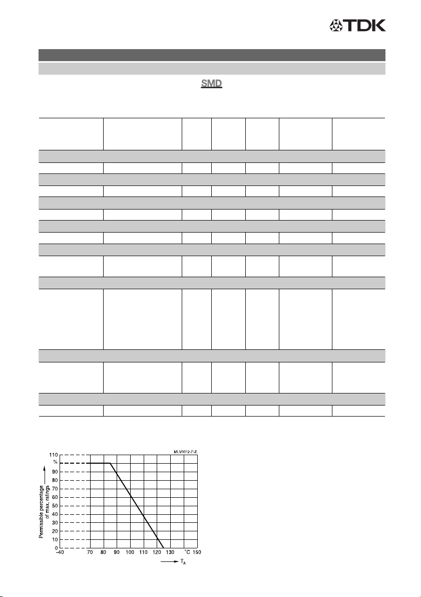
No change in ESD protection performance at temperatures
up to 85 °C (temperature derating)
Low parasitic inductance
Low leakage current
Fast response time <0.5 ns
Lead-free nickel barrier terminations suitable for lead-free soldering
RoHS-compatible
Applications
Interfaces, data lines (USB, IEEE 1394, Ethernet, parallel port,
SATA, DisplayPort, etc.), audio lines (digital) and video lines
(analog), DVI, HDMI, ICs and I/O ports
Consumer electronic products (TV, DVD player/recorder, set-top
box, game consoles, MP3 player, digital still/video camera, etc.)
EDP products (desktop and notebook computer, monitor, PDA,
printer, memory card, control unit, head set, speaker, HDD, optical
drive, etc.)
Industrial applications
Mobile phone applications
Design
Multilayer technology
Nickel barrier termination (Ag/Ni/Sn) for lead-free soldering
Marking
Due to the symmetrical configuration no marking information is
needed.
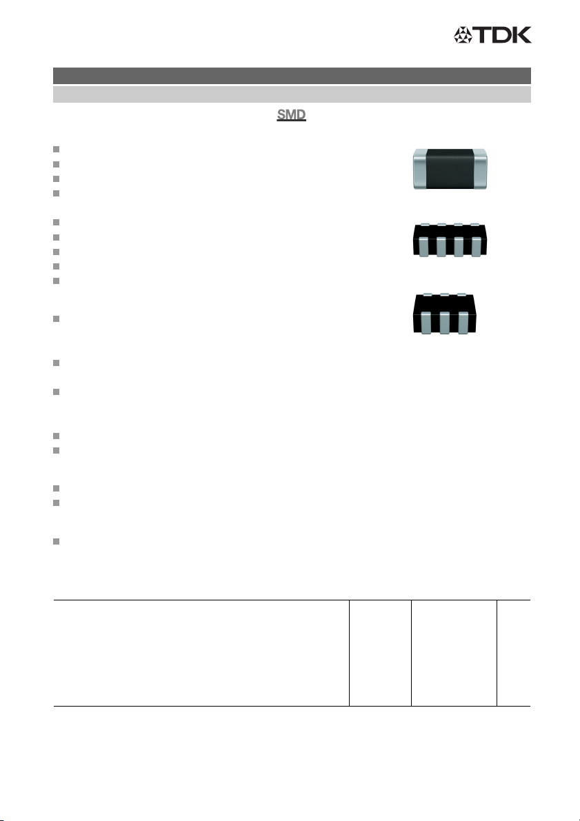
Single chip
4-fold array
2/4 data + 1 supply
General technical data
Maximum DC operating voltage V
Typical capacitance C
Air discharge ESD capability to IEC 61000-4-2 V
Contact discharge ESD capability to IEC 61000-4-2 V
Leakage current (V
= 5.6 V) I
leak
Operating temperature T
DC,max
typ
ESD,air
ESD,contact
leak
op
5.5 ... 30 V
0.6 ... 10 pF
15 kV
8 kV
1 µA
40/+85 °C
Storage temperature LCT/UCT 40/+125 °C
Important notes at the end of this document.
Page 2 of 22Please read Cautions and warnings and
Page 3
CeraDiodes
High-speed series
Electrical specifications and ordering codes
Maximum ratings (T
Type Ordering code
= 85 °C) and characteristics (TA= 25 °C)
op,max
V
V
DC,max
BR,min
(1 mA)
V
V
V
clamp,max
(1 A)
V
C
typ
(1 MHz, 1 V)
pF
C
max
(1 MHz, 1 V)
pF
Array, 2/4 data + 1 supply, 0506, SOT-666
CDA3C05GTH B72755D0050H062 5.6 106 395 2.2 3.5
Array, 2/4 data + 1 supply, 1012, SOT-23 6L
CDA6C05GTH B72735D0050H062 5.6 52 195 7 10
Array, 4-fold, 0508, no semiconductor diode equivalent
CDA4C16GTH B72714D0160H060 16 22 66 10 15
Array, 4-fold, 0612, no semiconductor diode equivalent
CDA5C16GTH B72724D0160H062 16 80 350 3 5
Single, 0201, no semiconductor diode equivalent
CDS1C05GTH1 B72440C0050H160 5.5 17 33 7 -
CDS1C05GTH2 B72440C0050H260 5.5 20 66 3 Single, 0402, SOD-723
CDS2C05HDMI1 B72590D0050H160 5.6 150 - 0.6 0.9
CDS2C05HDMI2 B72590D0050H260 5.6 90 - 0.6 0.9
CDS2C12GTH B72590D0120H060 12 20 66 4.5 CDS2C15GTH B72590D0150H060 15 23 66 10 15
CDS2C16GTH B72590D0160H060 16 65 290 2 3
CDS2C20GTH B72590D0200H060 20 30 80 10 13
Single, 0603, SOD-523
CDS3C05HDMI1 B72500D0050H160 5.6 150 - 0.6 0.9
CDS3C16GTH B72500D0160H060 16 65 290 3 5
CDS3C30GTH B72500D0300H060 30 50 120 10 15
Single, 1003, SOD-323
CDS4C16GTH B72570D0160H060 16 38 146 3 5
Typical characteristics
Important notes at the end of this document.
Page 3 of 22Please read Cautions and warnings and
Page 4
CeraDiodes
High-speed series
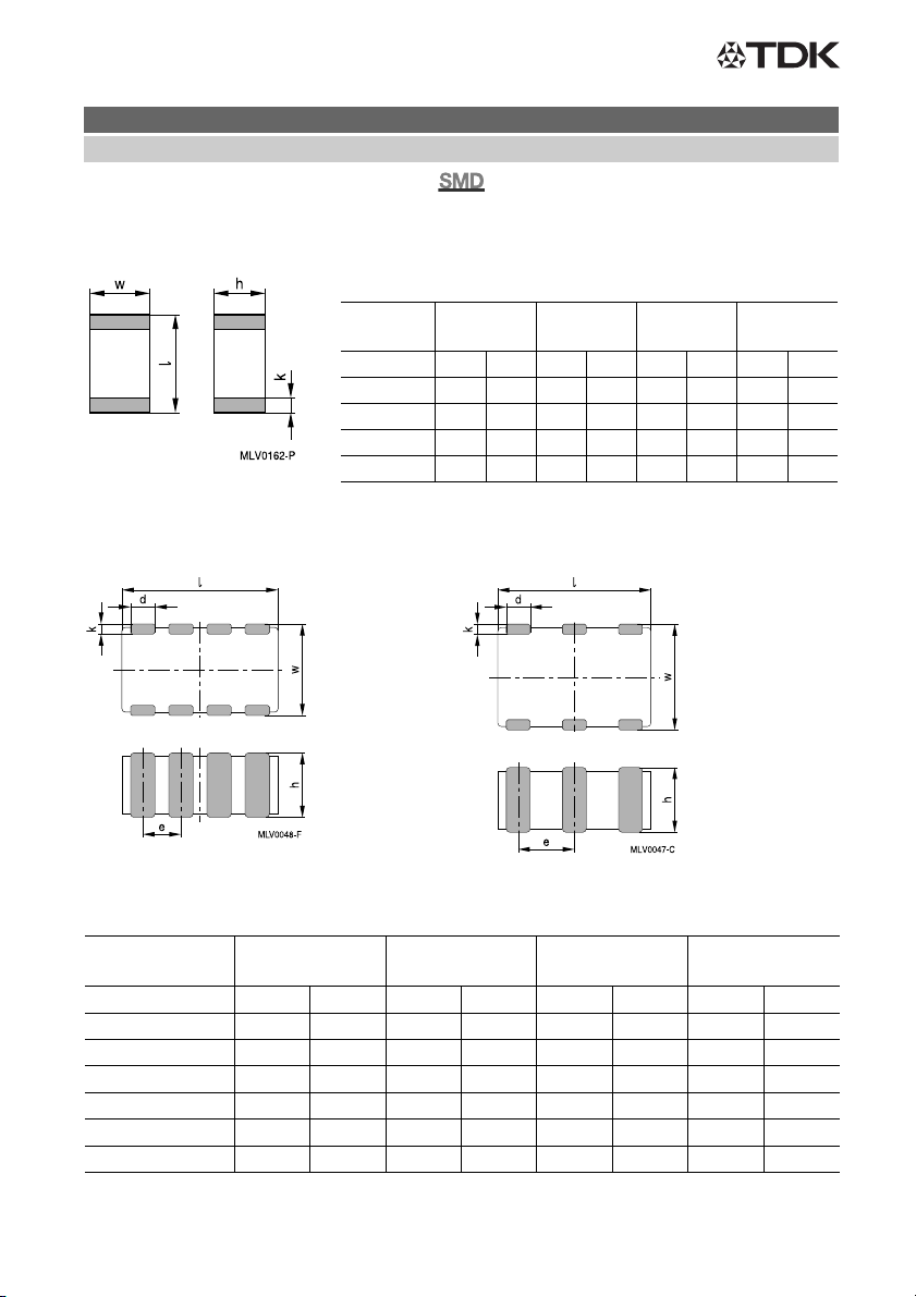
Dimensional drawings
Single device
Dimensions in mm
Case
(inch)
size
(mm)
0201
0603
0402
1005
Min. Max. Min. Max. Min. Max. Min. Max.
l 0.57 0.63 0.85 1.15 1.45 1.75 2.34 2.74
w 0.27 0.33 0.4 0.6 0.7 0.9 0.7 0.9
h 0.27 0.33 0.4 0.6 0.7 0.9 0.7 0.9
k 0.1 0.2 0.1 0.3 0.1 0.4 0.13 0.75
Array devices
4-fold array 2/4 data + 1 supply
0603
1608
1003
2508
Dimension in mm
Case size (inch)
(mm)
0506
1216
0508
1220
0612
1632
1012
2532
Min. Max. Min. Max. Min. Max. Min. Max.
l 1.50 1.70 1.8 2.2 3.0 3.4 2.90 3.50
w 1.20 1.40 1.05 1.45 1.45 1.75 2.25 2.75
h - 0.6 - 0.9 - 0.9 - 1.2
d 0.2 0.4 0.2 0.4 0.25 0.55 0.35 0.65
e 0.4 0.6 0.4 0.6 0.61 0.91 0.8 1.1
k - 0.35 - 0.35 - 0.35 - 0.45
Important notes at the end of this document.
Page 4 of 22Please read Cautions and warnings and
Page 5
CeraDiodes
High-speed series
Recommended solder pads
Single device
Dimensions in mm
Case size (inch)
(mm)
A 0.3 0.6 1.0 0.8
B 0.25 0.6 1.0 0.8
C 0.3 0.5 1.0 1.45
Array devices
4-fold array 2/4 data + 1 supply
0201
0603
0402
1005
0603
1608
1003
2508
Dimensions in mm
Case size (inch)
(mm)
A
B
C
E
Important notes at the end of this document.
0506
1216
0.36 0.35 0.5 0.7
0.84 0.9 0.7 1.0
0.62 0.4 1.2 1.4
0.50 0.5 0.76 0.95
0508
1220
Page 5 of 22Please read Cautions and warnings and
0612
1632
1012
2532
Page 6
CeraDiodes
High-speed series
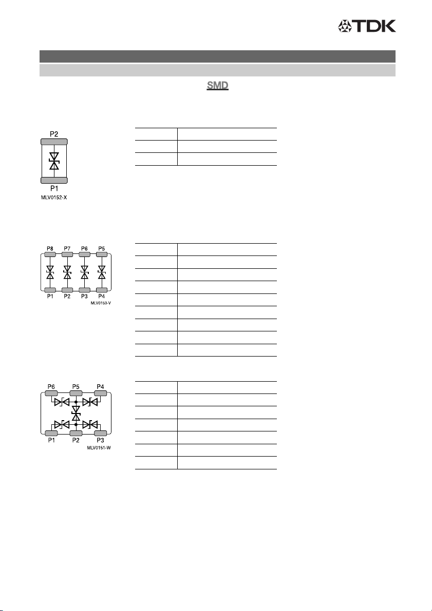
Pin configurations
Single device
Array devices
4-fold array
Pin Description
P1 GND
P2 I/O line
Pin Description
P1 GND
P2 GND
P3 GND
P4 GND
P5 I/O line 1
P6 I/O line 2
P7 I/O line 3
P8 I/O line 4
2/4 data + 1 supply
Pin Description
P1 I/O line 1
P2 GND
P3 I/O line 2
P4 I/O line 3
P5 V
P6 I/O line 4
Important notes at the end of this document.
DC
Page 6 of 22Please read Cautions and warnings and
Page 7
CeraDiodes
High-speed series
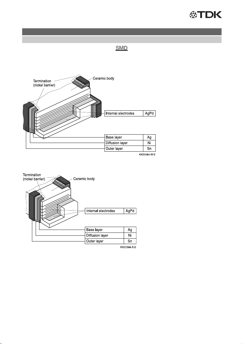
Termination
Single device
Array device
Important notes at the end of this document.
Page 7 of 22Please read Cautions and warnings and
Page 8

CeraDiodes
High-speed series
Delivery mode
EIA case size Taping Reel sizemmPacking unit
Type Ordering code
pcs.
0201 Cardboard 180 15000 CDS1C05GTH1 B72440C0050H160
0201 Cardboard 180 15000 CDS1C05GTH2 B72440C0050H260
0402 Cardboard 180 10000 CDS2C05HDMI1 B72590D0050H160
0402 Cardboard 180 10000 CDS2C05HDMI2 B72590D0050H260
0402 Cardboard 180 10000 CDS2C12GTH B72590D0120H060
0402 Cardboard 180 10000 CDS2C15GTH B72590D0150H060
0402 Cardboard 180 10000 CDS2C16GTH B72590D0160H060
0402 Cardboard 180 10000 CDS2C20GTH B72590D0200H060
0506 Blister 180 3000 CDA3C05GTH B72755D0050H062
0508 Cardboard 180 4000 CDA4C16GTH B72714D0160H060
0603 Cardboard 180 4000 CDS3C05HDMI1 B72500D0050H160
0603 Cardboard 180 4000 CDS3C16GTH B72500D0160H060
0603 Cardboard 180 4000 CDS3C30GTH B72500D0300H060
0612 Blister 180 3000 CDA5C16GTH B72724D0160H062
1003 Cardboard 180 4000 CDS4C16GTH B72570D0160H060
1012 Blister 180 2000 CDA6C05GTH B72735D0050H062
Important notes at the end of this document.
Page 8 of 22Please read Cautions and warnings and
Page 9

CeraDiodes
High-speed series
1 Taping and packing for chip and array CeraDiodes
1.1 Cardboard tape (taping to IEC 60286-3)
Dimensions in mm
Case size (inch) 0201
(mm)
0603 1005 1608 2508 1220
0402 0603 1003 0508 Tolerance
Compartment width A00.38 ±0.05 0.6 0.95 1.0 1.6 ±0.2
Compartment length B00.68 ±0.05 1.15 1.8 2.85 2.4 ±0.2
Sprocket hole diameter D01.5 ±0.1 1.5 1.5 1.5 1.5 +0.1/ 0
Sprocket hole pitch P04.0 ±0.11)4.0 4.0 4.0 4.0 ±0.1
Distance center hole to center
P22.0 ±0.05 2.0 2.0 2.0 2.0 ±0.05
1)
compartment
Pitch of component compartments P12.0 ±0.05 2.0 4.0 4.0 4.0 ±0.1
Tape width W 8.0 ±0.3 8.0 8.0 8.0 8.0 ±0.3
Distance edge to center of hole E 1.75 ±0.1 1.75 1.75 1.75 1.75 ±0.1
Distance center hole to center
F 3.5 ±0.05 3.5 3.5 3.5 3.5 ±0.05
compartment
Distance compartment to edge G 1.35 min. 0.75 0.75 0.75 0.75 min.
Thickness tape T 0.35 ±0.02 0.6 0.9 1.0 0.95 max.
Overall thickness T20.4 min. 0.7 1.1 1.1 1.12 max.
1)
≤ ±0.2 mm over 10 sprocket holes
Important notes at the end of this document.
Page 9 of 22Please read Cautions and warnings and
Page 10

CeraDiodes
High-speed series
1.2 Blister tape (taping to IEC 60286-3)
Dimensions in mm
Case size (inch)
(mm)
0506
1216
0612
1632
1012
2532
Tolerance
Compartment width A01.5 1.9 2.8 ±0.2
Compartment length B01.8 3.5 3.5 ±0.2
Compartment height K00.8 1.8 1.8 max.
Sprocket hole diameter D01.5 1.5 1.5 +0.1/ 0
Compartment hole diameter D11.0 1.0 1.0 min.
Sprocket hole pitch P04.0 4.0 4.0 ±0.1
Distance center hole to center
P22.0 2.0 2.0 ±0.05
1)
compartment
Pitch of component compartments P14.0 4.0 4.0 ±0.1
Tape width W 8.0 8.0 8.0 ±0.3
Distance edge to center of hole E 1.75 1.75 1.75 ±0.1
Distance center hole to center
F 3.5 3.5 3.5 ±0.05
compartment
Distance compartment to edge G 0.75 0.75 0.75 min.
Thickness tape T 0.3 0.3 0.3 max.
Overall thickness T21.3 2.5 2.5 max.
1)
≤ ±0.2 mm over 10 sprocket holes
Important notes at the end of this document.
Page 10 of 22Please read Cautions and warnings and
Page 11

CeraDiodes
High-speed series
1.3 Reel packing
Dimensions in mm
Dimensions Tolerance Dimensions Tolerance
Reel diameter A 180 +0/ –3 330 ±2
Reel width (inside) W
Reel width (outside) W
8.4 +1.5/ –0 8.4 +1.5/ –0
1
14.4 max. 14.4 max.
2
Package: 8-mm tape
Reel material: Plastic
1.4 Packing units
Case size
(inch) / (mm)
∅ 180-mm reel
pieces
∅ 330-mm reel
pieces
Tape
0201 / 0603 15000 - cardboard
0402 / 1005 10000 50000 cardboard
0603 / 1608 4000 16000 cardboard
1003 / 2508 4000 16000 cardboard
0506 / 1216 3000 12000 blister
0508 / 1220 4000 16000 cardboard
0612 / 1632 3000 12000 blister
1012 / 2532 2000 8000 blister
Important notes at the end of this document.
Page 11 of 22Please read Cautions and warnings and
Page 12

CeraDiodes
High-speed series
Soldering directions
1 Reflow soldering temperature profile
Recommended temperature characteristic for reflow soldering following
JEDEC J-STD-020D
Profile feature Sn-Pb eutectic assembly Pb-free assembly
Preheat and soak
- Temperature min T
- Temperature max T
- Time t
Average ramp-up rate T
Liquidous temperature T
Time at liquidous t
Peak package body temperature T
smin
L
smin
smax
smax
L
1)
p
to t
Time (tP)3)within 5 °C of specified
classification temperature (Tc)
Average ramp-down rate Tpto T
100 °C 150 °C
150 °C 200 °C
60 ... 120 s 60 ... 180 s
smax
to Tp3 °C/ s max. 3 °C/ s max.
183 °C 217 °C
60 ... 150 s 60 ... 150 s
220 °C ... 235 °C
3)
20 s
6 °C/ s max. 6 °C/ s max.
smax
2)
245 °C ... 260 °C
3)
30 s
2)
Time 25 °C to peak temperature maximum 6 min maximum 8 min
1) Tolerance for peak profile temperature (TP) is defined as a supplier minimum and a user maximum.
2) Depending on package thickness. For details please refer to JEDEC J-STD-020D.
3) Tolerance for time at peak profile temperature (tP) is defined as a supplier minimum and a user maximum.
Note: All temperatures refer to topside of the package, measured on the package body surface.
Number of reflow cycles: 3
Important notes at the end of this document.
Page 12 of 22Please read Cautions and warnings and
Page 13

CeraDiodes
High-speed series
2 Soldering guidelines
The use of mild, non-activated fluxes for soldering is recommended, as well as proper cleaning of
the PCB.
The components are suitable for reflow soldering to JEDEC J-STD-020D.
3 Solder joint profiles / solder quantity
3.1 Cement quantity
The component is fixed onto the circuit board with cement prior to soldering. It must still be able
to move slightly. When the board is placed into the reflow oven, excessively rigid fixing can lead
to high forces acting on the component and thus to a break. In addition, too much cement can
lead to unsymmetrical stressing and thus to mechanical fracture of the component. The cement
must also be so soft during mounting that no mechanical stressing occurs.
3.2 Mounting the components on the board
It is best to mount the components on the board before soldering so that one termination does not
enter the oven first and the second termination is soldered subsequently. The ideal case is simultaneous wetting of both terminations.
3.3 Solder joint profiles
If the meniscus height is too low, that means the solder quantity is too low, the solder joint may
break, i.e. the component becomes detached from the joint. This problem is sometimes interpreted as leaching of the external terminations.
If the solder meniscus is too high, i.e. the solder quantity is too large, the vise effect may occur.
As the solder cools down, the solder contracts in the direction of the component. If there is too
much solder on the component, it has no leeway to evade the stress and may break, as in a vise.
Important notes at the end of this document.
Page 13 of 22Please read Cautions and warnings and
Page 14

CeraDiodes
High-speed series
3.3.1 Solder joint profiles for nickel barrier termination
Good and poor solder joints caused by amount of solder in infrared reflow soldering
Important notes at the end of this document.
Page 14 of 22Please read Cautions and warnings and
Page 15

CeraDiodes
High-speed series
4 Solderability tests
Test Standard Test conditions /
Sn-Pb soldering
Wettability IEC
60068-2-58
Immersion in
60/40 SnPb solder
using non-activated
flux at 215 ±3 °C for
3 ±0.3 s
Test conditions /
Pb-free soldering
Immersion in
Sn96.5Ag3.0Cu0.5
solder using non- or
low activated flux
at 245 ±5 °C
Criteria / test results
Covering of 95%
of end termination,
checked by visual
inspection
for 3 ±0.3 s
Leaching
resistance
Tests of
resistance to
soldering heat
IEC
60068-2-58
IEC
60068-2-58
Immersion in
60/40 SnPb
solder using
mildly activated flux
without preheating
at 255 ±5 °C
for 10 ±1 s
Immersion in
60/40 SnPb for 10 s
at 260 °C
Immersion in
Sn96.5Ag3.0Cu0.5
solder using non- or
low activated flux
without preheating
at 255 ±5 °C
for 10 ±1 s
Immersion in
Sn96.5Ag3.0Cu0.5
for 10 s at 260 °C
No leaching of
contacts
Capacitance change:
15% ≤∆C ≤15%
for SMDs
Note:
Leaching of the termination
Effective area at the termination might be lost if the soldering temperature and/or immersion time
are not kept within the recommended conditions. Leaching of the outer electrode should not exceed 25% of the chip end area (full length of the edge A-B-C-D) and 25% of the length A-B,
shown below as mounted on the substrate.
As single chip As mounted on substrate
Important notes at the end of this document.
Page 15 of 22Please read Cautions and warnings and
Page 16

CeraDiodes
High-speed series
5 Notes for proper soldering
5.1 Preheating and cooling
The average ramp-up rate must not exceed 3 °C/s.
The cooling rate must not exceed 8 °C/s.
5.2 Repair / rework
Manual soldering with a soldering iron must be avoided, hot-air methods are recommended for
making repairs.
5.3 Cleaning
All environmentally compatible agents are suitable for cleaning. Select the appropriate cleaning
solution according to the type of flux used. The temperature difference between the components
and cleaning liquid must not be greater than 100 °C. Ultrasonic cleaning should be carried out
with the utmost caution. Too high ultrasonic power can impair the adhesive strength of the metallized surfaces. Insufficient or excessive cleaning can be detrimental to CeraDiode performance.
5.4 Solder paste printing (reflow soldering)
An excessive application of solder paste results in too high a solder fillet, thus making the chip
more susceptible to mechanical and thermal stress. This will lead to the formation of cracks. Too
little solder paste reduces the adhesive strength on the outer electrodes and thus weakens the
bonding to the PCB. The solder should be applied smoothly to the end surface to a height of
min. 0.2 mm.
5.5 Selection of flux
Used flux should have less than or equal to 0.1 wt % of halogenated content, since flux residue
after soldering could lead to corrosion of the termination and/or increased leakage current on the
surface of the CeraDiode. Strong acidic flux must not be used. The amount of flux applied should
be carefully controlled, since an excess may generate flux gas, which in turn is detrimental to solderability.
5.6 Storage
Solderability is guaranteed for one year from date of delivery, provided that components are
stored in their original packages.
Storage temperature: 25 °C to +45 °C
Relative humidity: ≤75% annual average, ≤95% on 30 days a year
The solderability of the external electrodes may deteriorate if SMDs are stored where they are exposed to high humidity, dust or harmful gas (hydrogen chloride, sulfurous acid gas or hydrogen
sulfide).
Do not store SMDs where they are exposed to heat or direct sunlight. Otherwise the packing material may be deformed or SMDs may stick together, causing problems during mounting.
After opening the factory seals, such as polyvinyl-sealed packages, it is recommended to use the
SMDs as soon as possible.
Important notes at the end of this document.
Page 16 of 22Please read Cautions and warnings and
Page 17

CeraDiodes
High-speed series
5.7 Placement of components on circuit board
It is of advantage to place the components on the board before soldering so that their two terminals do not enter the solder oven at different times. Ideally, both terminals should be wetted simultaneously.
5.8 Soldering caution
Sudden heating or cooling of the component results in thermal destruction by cracks.
An excessively long soldering time or high soldering temperature results in leaching of the outer electrodes, causing poor adhesion due to loss of contact between electrodes and termination.
Avoid manual soldering with a soldering iron.
Wave soldering must not be applied for CeraDiodes designated for reflow soldering only.
Keep to the recommended down-cooling rate.
5.9 Standards
CECC 00802
IEC 60068-2-58
IEC 60068-2-20
JEDEC J-STD-020D
Important notes at the end of this document.
Page 17 of 22Please read Cautions and warnings and
Page 18

CeraDiodes
High-speed series
Symbols and terms
CeraDiode Semiconductor diode
C
max
C
typ
I
BR
I
leak
I
PP
P
PP
IR, I
I
RM
IP, I
P
T
PP
PP
Maximum capacitance
Typical capacitance
(Reverse) current @ breakdown voltage
(Reverse) leakage current
Current @ clamping voltage, peak pulse
current
Peak pulse power
T
op
T
stg
V
BR
V
BR,min
V
clamp
V
clamp,max
V
DC
V
BR
V
cl,VC
VRM, V
RWM
, VWM, V
DC
Operating temperature
Storage temperature
(Reverse) breakdown voltage
Minimum breakdown voltage
Clamping voltage
Maximum clamping voltage
(Reverse) stand-off voltage, working
voltage, operating voltage
V
DC,max
V
ESD,air
V
ESD,contact
V
leak
- *) I
VRM, V
F
- *) IRM, I
, VWM, V
RWM
RM,max@VRM
DC
Maximum DC operating voltage
Air discharge ESD capability
Contact discharge ESD capability
(Reverse) voltage @ leakage current
Current @ forward voltage
(Reverse) current @ maximum reverse
stand-off voltage, working voltage,
operating voltage
- *) V
F
Forward voltage
*) Not applicable due to bidirectional characteristics of CeraDiodes
Important notes at the end of this document.
Page 18 of 22Please read Cautions and warnings and
Page 19

CeraDiodes
High-speed series
Cautions and warnings
General
Some parts of this publication contain statements about the suitability of our CeraDiodes for certain areas of application, including recommendations about incorporation/design-in of these products into customer applications. The statements are based on our knowledge of typical requirements often made of our CeraDiodes in the particular areas. We nevertheless expressly point out
that such statements cannot be regarded as binding statements about the suitability of our
CeraDiodes for a particular customer application. As a rule, EPCOS is either unfamiliar with individual customer applications or less familiar with them than the customers themselves. For these
reasons, it is always incumbent on the customer to check and decide whether the CeraDiodes
with the properties described in the product specification are suitable for use in a particular customer application.
Do not use EPCOS CeraDiodes for purposes not identified in our specifications, application
notes and data books.
Ensure the suitability of a CeraDiode in particular by testing it for reliability during design-in. Always evaluate a CeraDiode under worst-case conditions.
Pay special attention to the reliability of CeraDiodes intended for use in safety-critical applications (e.g. medical equipment, automotive, spacecraft, nuclear power plant).
Design notes
Always connect a CeraDiode in parallel with the electronic circuit to be protected.
Consider maximum rated power dissipation if a CeraDiode has insufficient time to cool down
between a number of pulses occurring within a specified isolated time period. Ensure that electrical characteristics do not degrade.
Consider derating at higher operating temperatures. Choose the highest voltage class compatible with derating at higher temperatures.
Surge currents beyond specified values will puncture a CeraDiode. In extreme cases a
CeraDiode will burst.
If steep surge current edges are to be expected, make sure your design is as low-inductance
as possible.
In some cases the malfunctioning of passive electronic components or failure before the end of
their service life cannot be completely ruled out in the current state of the art, even if they are
operated as specified. Do not use CeraDiodes in applications requiring a very high level of operational safety and especially when the malfunction or failure of a passive electronic component could endanger human life or health (e.g. in accident prevention, life-saving systems, or
automotive battery line applications such as clamp 30), ensure by suitable design of the application or other measures (e.g. installation of protective circuitry or redundancy) that no injury or
damage is sustained by third parties in the event of such a malfunction or failure.
Specified values only apply to CeraDiodes that have not been subject to prior electrical, mechanical or thermal damage. The use of CeraDiodes in line-to-ground applications is therefore
not advisable, and it is only allowed together with safety countermeasures like thermal fuses.
Important notes at the end of this document.
Page 19 of 22Please read Cautions and warnings and
Page 20

CeraDiodes
High-speed series
Storage
Only store CeraDiodes in their original packaging. Do not open the package before storage.
Storage conditions in original packaging: temperature -25 to +45°C, relative humidity ≤75% annual average, maximum 95%, dew precipitation is inadmissible.
Do not store CeraDiodes where they are exposed to heat or direct sunlight. Otherwise the
packaging material may be deformed or CeraDiodes may stick together, causing problems during mounting.
Avoid contamination of the CeraDiode surface during storage, handling and processing.
Avoid storing CeraDiodes in harmful environments where they are exposed to corrosive gases
for example (SOx, Cl).
Use CeraDiodes as soon as possible after opening factory seals such as polyvinyl-sealed packages.
Solder CeraDiodes after shipment from EPCOS within the time specified: 12 months.
Handling
Do not drop CeraDiodes and allow them to be chipped.
Do not touch CeraDiodes with your bare hands - gloves are recommended.
Avoid contamination of the CeraDiode surface during handling.
Washing processes may damage the product due to the possible static or cyclic mechanical
loads (e.g. ultrasonic cleaning). They may cause cracks to develop on the product and its parts,
which might lead to reduced reliability or lifetime.
Mounting
When CeraDiodes are encapsulated with sealing material or overmolded with plastic material,
be aware that potting, sealing or adhesive compounds can produce chemical reactions in the
CeraDiode ceramic that will degrade its electrical characteristics and reduce its lifetime.
Make sure an electrode is not scratched before, during or after the mounting process.
Make sure contacts and housings used for assembly with CeraDiodes are clean before mounting.
The surface temperature of an operating CeraDiode can be higher. Ensure that adjacent components are placed at a sufficient distance from a CeraDiode to allow proper cooling.
Avoid contamination of the CeraDiode surface during processing.
Only CeraDiodes with an Ni barrier termination are approved for lead-free soldering.
Soldering
Complete removal of flux is recommended to avoid surface contamination that can result in an
instable and/or high leakage current.
Use resin-type or non-activated flux.
Bear in mind that insufficient preheating may cause ceramic cracks.
Rapid cooling by dipping in solvent is not recommended, otherwise a component may crack.
Important notes at the end of this document.
Page 20 of 22Please read Cautions and warnings and
Page 21

CeraDiodes
High-speed series
Operation
Use CeraDiodes only within the specified operating temperature range.
Use CeraDiodes only within specified voltage and current ranges.
Environmental conditions must not harm a CeraDiode. Only use them in normal atmospheric
conditions. Reducing the atmosphere (e.g. hydrogen or nitrogen atmosphere) is prohibited.
Prevent a CeraDiode from contacting liquids and solvents. Make sure that no water enters a
CeraDiode (e.g. through plug terminals).
Avoid dewing and condensation.
EPCOS CeraDiodes are designed for encased applications. Under all circumstances avoid exposure to:
direct sunlight
rain or condensation
steam, saline spray
corrosive gases
atmosphere with reduced oxygen content
EPCOS CeraDiodes are not suitable for switching applications or voltage stabilization where
static power dissipation is required.
This listing does not claim to be complete, it merely reflects the experience of EPCOS AG.
Display of ordering codes for EPCOS products
The ordering code for one and the same EPCOS product can be represented differently in data
sheets, data books, other publications, on the EPCOS website, or in order-related documents
such as shipping notes, order confirmations and product labels. The varying representations of
the ordering codes are due to different processes employed and do not affect the
specifications of the respective products. Detailed information can be found on the Internet
under www.epcos.com/orderingcodes
Important notes at the end of this document.
Page 21 of 22Please read Cautions and warnings and
Page 22

Important notes
The following applies to all products named in this publication:
1. Some parts of this publication contain statements about the suitability of our products for
certain areas of application. These statements are based on our knowledge of typical re-
quirements that are often placed on our products in the areas of application concerned. We
nevertheless expressly point out that such statements cannot be regarded as binding
statements about the suitability of our products for a particular customer application.
As a rule, EPCOS is either unfamiliar with individual customer applications or less familiar
with them than the customers themselves. For these reasons, it is always ultimately incumbent on the customer to check and decide whether an EPCOS product with the properties described in the product specification is suitable for use in a particular customer application.
2. We also point out that in individual cases, a malfunction of electronic components or
failure before the end of their usual service life cannot be completely ruled out in the
current state of the art, even if they are operated as specified. In customer applications
requiring a very high level of operational safety and especially in customer applications in
which the malfunction or failure of an electronic component could endanger human life or
health (e.g. in accident prevention or lifesaving systems), it must therefore be ensured by
means of suitable design of the customer application or other action taken by the customer
(e.g. installation of protective circuitry or redundancy) that no injury or damage is sustained by
third parties in the event of malfunction or failure of an electronic component.
3. The warnings, cautions and product-specific notes must be observed.
4. In order to satisfy certain technical requirements, some of the products described in this
publication may contain substances subject to restrictions in certain jurisdictions (e.g.
because they are classed as hazardous). Useful information on this will be found in our Ma-
terial Data Sheets on the Internet (www.epcos.com/material). Should you have any more detailed questions, please contact our sales offices.
5. We constantly strive to improve our products. Consequently, the products described in this
publication may change from time to time. The same is true of the corresponding product
specifications. Please check therefore to what extent product descriptions and specifications
contained in this publication are still applicable before or when you place an order. We also
reserve the right to discontinue production and delivery of products. Consequently, we
cannot guarantee that all products named in this publication will always be available. The
aforementioned does not apply in the case of individual agreements deviating from the foregoing for customer-specific products.
6. Unless otherwise agreed in individual contracts, all orders are subject to the current ver-
sion of the "General Terms of Delivery for Products and Services in the Electrical Industry" published by the German Electrical and Electronics Industry Association
(ZVEI).
7. The trade names EPCOS, Alu-X, CeraDiode, CeraLink, CeraPlas, CSMP, CSSP, CTVS,
DeltaCap, DigiSiMic, DSSP, FilterCap, FormFit, MiniBlue, MiniCell, MKD, MKK, MLSC,
MotorCap, PCC, PhaseCap, PhaseCube, PhaseMod, PhiCap, PQSine, SIFERRIT, SIFI,
SIKOREL, SilverCap, SIMDAD, SiMic, SIMID, SineFormer, SIOV, SIP5D, SIP5K, TFAP,
ThermoFuse, WindCap are trademarks registered or pending in Europe and in other countries. Further information will be found on the Internet at www.epcos.com/trademarks.
Page 22 of 22
 Loading...