

查询B82442-A1535-A300供应商
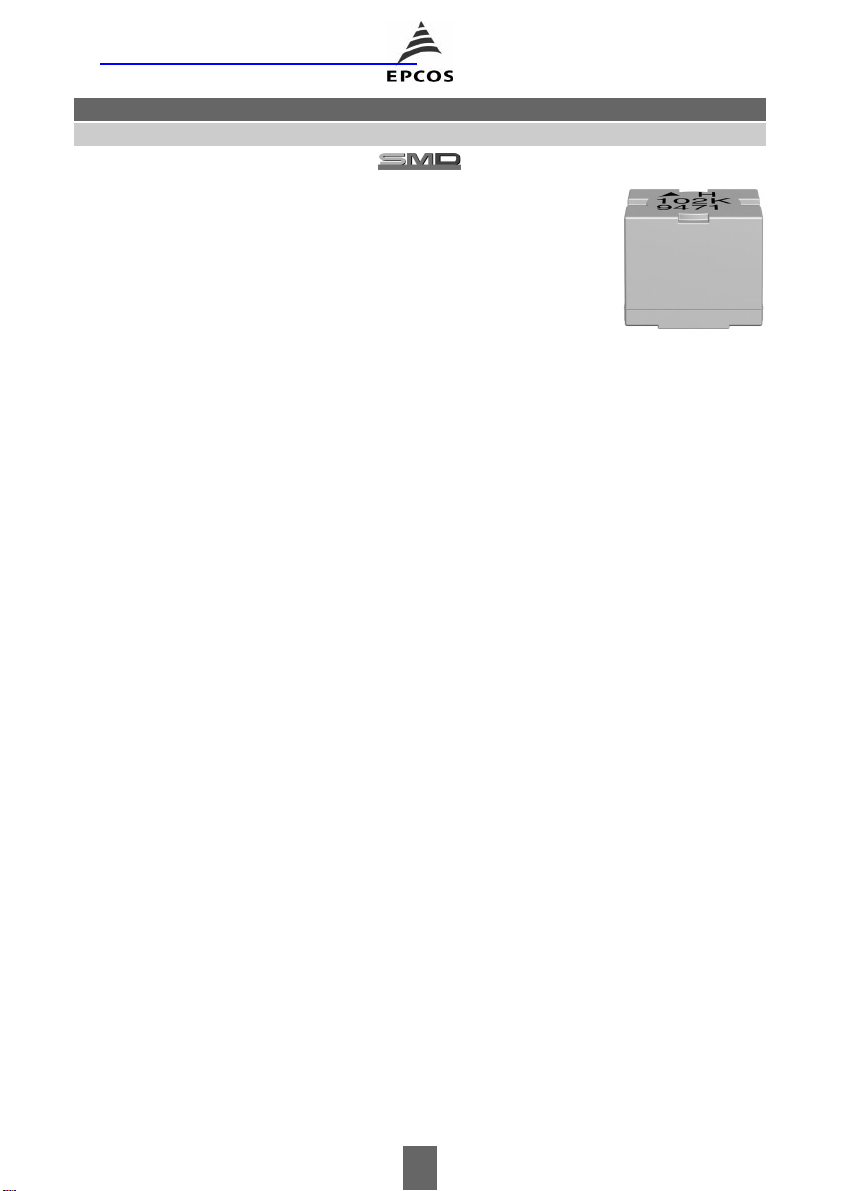
SIMID 2220-H
High-current version
Size 2220 (EIA) or 5650 (IEC)
Rated inductance 1 to 10000 µH
Rated current 35 to 2500 mA
Construction
■ Upright ferrite drum core
■ Laser-welded winding
■ Flame-retardant encapsulation
Features
■ Very high current handling capability
■ High
L
values
■ Suitable for reflow (IR and vapor phase) and wave soldering
Applications
■ Filtering of supply voltages, coupling, decoupling
■ DC/DC converters
■ Automotive electronics
■ Telecommunications
Terminals
■ Tinned
■ 0,4 µm Cu; 1–2 µm Ag; 5–7 µm Sn
■ Base material CuSn6
■ No leaching during wave soldering
B82442-HSMT Inductors, SIMID Series
Marking
Marking on component:
Manufacturer,
L
value (in nH) and tolerance ofL value (coded),
date of manufacture (coded)
Minimum data on reel:
Manufacturer, part number, ordering code,
L
value and tolerance ofL value,
quantity, date of packing
Delivery mode
12-mm blister tape, wound on 330-mm ∅ reel
For details on taping, packing and packing units see page 153
135 04/00
SIMID 2220-H
General technical data
B82442-HSMT Inductors, SIMID Series
Rated inductance
Q factor
Q
Rated current
min
L
R
Measured with impedance analyzer HP 4194A
at frequency
f
L
Measured with impedance analyzer HP 4194A
at frequency
I
R
Maximum permissible dc with
inductance decrease ∆L/
f
Q
L
≤ 10 %
0
and temperature increase of ≤ 40 K
at rated temperature of 85°C
Self-resonance frequency
DC resistance
R
max
f
res, min
Measured with network analyzer HP 8753
Measured at 20°C ambient temperature,
measuring current <
I
R
Climatic category In accordance with IEC 60068-1
55/125/56 (– 55°C/+ 125°C/56 days damp heat test)
Solderability In accordance with IEC 60062-2-58
(215 ± 3)°C, (3 ± 0,3) s
Wetting of soldering area: ≥ 90 %
Resistance to soldering heat In accordance with IEC 60068-2-20
260°C, 10 s
∆L/L≤ ± 3%
Permissible PCB bending 2 mm (100 mm long standard PCB)
Weight Approx. 400 mg
136 04/00
SIMID 2220-H
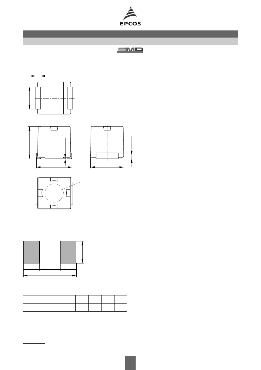
Dimensional drawing
1)
0,7±0,2
1)
3,5±0,1
5+0,3
0,15 max.
B82442-HSMT Inductors, SIMID Series
1)
0,7 min.
5,6+0,3
Marking
Marking
5+0,3
SSB1261-E
Layout recommendation
A
CB
B
D
SSB1227-Z
Dimensions (mm)
ABCD
Wave/reflow soldering 4,5 2,0 4,0 8,0
1) Soldering area, tinned
137 04/00
B82442-HSMT Inductors, SIMID Series
SIMID 2220-H
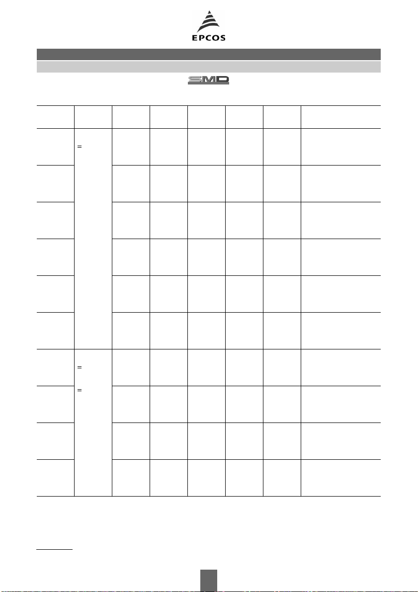
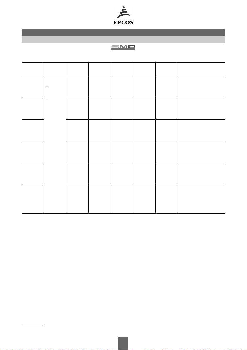
Characteristics and ordering codes
L
µH
R
Tolerance
Q
min
f
;
L
MHz
f
I
Q
R
mA
R
max
Ω
f
res, min
MHz
Ordering code
1)
1,0 ± 10 % K10 7,96 2500 0,024 95 B82442-H1102-K
1,2 10 7,96 2350 0,028 70 B82442-H1122-K
^
1,5 10 7,96 2200 0,032 55 B82442-H1152-K
1,8 10 7,96 2000 0,040 47 B82442-H1182-K
2,2 10 7,96 1800 0,048 42 B82442-H1222-K
2,7 10 7,96 1700 0,056 37 B82442-H1272-K
3,3 10 7,96 1550 0,064 34 B82442-H1332-K
3,9 10 7,96 1450 0,072 32 B82442-H1392-K
4,7 10 7,96 1350 0,088 29 B82442-H1472-K
5,6 10 7,96 1250 0,104 26 B82442-H1562-K
6,8 10 7,96 1130 0,120 24 B82442-H1682-K
8,2 10 7,96 1050 0,144 22 B82442-H1822-K
10 10 2,52 1000 0,168 19 B82442-H1103-K
12 10 2,52 880 0,20 17 B82442-H1123-K
15 10 2,52 810 0,24 16 B82442-H1153-K
18 10 2,52 740 0,29 14 B82442-H1183-K
22 10 2,52 670 0,35 13 B82442-H1223-K
27 10 2,52 620 0,42 11,5 B82442-H1273-K
33 ± 5 %
^
39 10 2,52 520 0,58 9,5 B82442-H1393-+
47 10 2,52 480 0,68 8,5 B82442-H1473-+
56 10 2,52 430 0,80 7,8 B82442-H1563-+
J
± 10 %
^
K
10 2,52 560 0,50 10,5 B82442-H1333-+
68 10 2,52 400 0,96 7,0 B82442-H1683-+
82 10 2,52 380 1,12 6,4 B82442-H1823-+
100 20 0,796 350 1,28 6,0 B82442-H1104-+
120 20 0,796 320 1,52 5,4 B82442-H1124-+
150 20 0,796 290 1,76 4,8 B82442-H1154-+
180 20 0,796 270 2,24 4,4 B82442-H1184-+
220 20 0,796 240 2,72 3,9 B82442-H1224-+
270 20 0,796 220 3,36 3,6 B82442-H1274-+
1) Replace the + by the code letter for the required inductance tolerance (see table).
138 04/00
B82442-HSMT Inductors, SIMID Series
SIMID 2220-H
Characteristics and ordering codes (continued)
L
R
µH
330 ± 5 %
390 20 0,796 180 4,64 2,9 B82442-H1394-+
470 20 0,796 170 5,60 2,6 B82442-H1474-+
560 20 0,796 150 6,80 2,4 B82442-H1564-+
Tolerance
^
J
± 10 %
^
K
Q
min
f
;
L
MHz
f
I
Q
R
mA
R
max
Ω
f
res, min
MHz
Ordering code
20 0,796 200 3,92 3,2 B82442-H1334-+
1)
680 20 0,796 140 8,00 2,2 B82442-H1684-+
820 20 0,796 130 10,4 2,0 B82442-H1824-+
1000 30 0,252 120 12,0 1,8 B82442-H1105-+
1200 30 0,252 105 13,6 1,5 B82442-H1125-+
1500 30 0,252 100 16,0 1,4 B82442-H1155-+
1800 30 0,252 85 24,0 1,3 B82442-H1185-+
2200 30 0,252 75 28,0 1,2 B82442-H1225-+
2700 30 0,252 65 44,0 1,1 B82442-H1275-+
3300 30 0,252 55 48,0 1,0 B82442-H1335-+
3900 30 0,252 53 56,0 1,0 B82442-H1395-+
4700 30 0,252 50 62,4 0,9 B82442-H1475-+
5600 30 0,252 46 68,0 0,8 B82442-H1565-+
6800 30 0,252 42 88,0 0,7 B82442-H1685-+
8200 30 0,252 39 100 0,6 B82442-H1825-+
10000 30 0,0796 35 120 0,5 B82442-H1106-+
1) Replace the + by the code letter for the required inductance tolerance (see table).
139 04/00

SIMID 2220-H
B82442-HSMT Inductors, SIMID Series
Impedance |Z|
versus frequency
f
measured with impedance analyzer
HP 4191A / HP 4194A
Q
factor versus frequency
f
measured with impedance analyzer
HP 4191A
80
Q
60
SSB1257-L
Inductance
versus dc load current
L
I
DC
measured with LCR meter
HP 4275A
Current derating
I
/
I
op
R
versus ambient temperature
1,2
I
Ι
op
B
I
Ι
R
R
1,0
0,8
T
A
SSB0893-E
40
20
0
10
1 µH
Hµ10
Hµ100
Hµ1000
15432
Hµ10000
10 10 10 10kHz
f
0,6
0,4
0,2
140 04/00
0
0
20 40 60 80 100 140C
T
A

 Loading...