

www.DataSheet4U.com
Metal Oxide Varistors CT0402S14AHSG
SMD multilayer varistor with Ni-barrier termination B72590T8140S160
Designation system
CT = Chip with three-layer- termination (Ag/Ni/Sn)
0402 = Dimensions of the device 04 x 02 (length x width in 1/100 inch)
S…A = Special tolerance of the varistor voltage
14 = Maximum operating voltage
HS = Designed for protection of high speed data lines
G = Taped version (cardboard tape, 7” reel, 10000 pieces/reel)
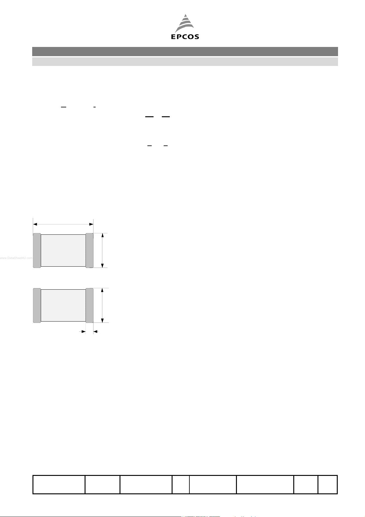
Figure
l
k
(all dimensions in mm)
b
l = 1.0 ± 0.15
b = 0.5 ± 0.10
s = 0.5 ± 0.10
k = 0.2 ± 0.10
s
As far as patents or other rights of third parties are concerned, liability is only assumed for components per se, not for
applications, processes and circuits implemented within components or assemblies. The information describes the type of
component and shall not be considered as assured characteristics. Terms of delivery and rights to change design reserved.
ISSUE DATE 28.01.2005 ISSUE e PUBLISHER KB VS PE PAGE 1/7
Metal Oxide Varistors CT0402S14AHSG
C
A
SMD multilayer varistor with Ni-barrier termination B72590T8140S160
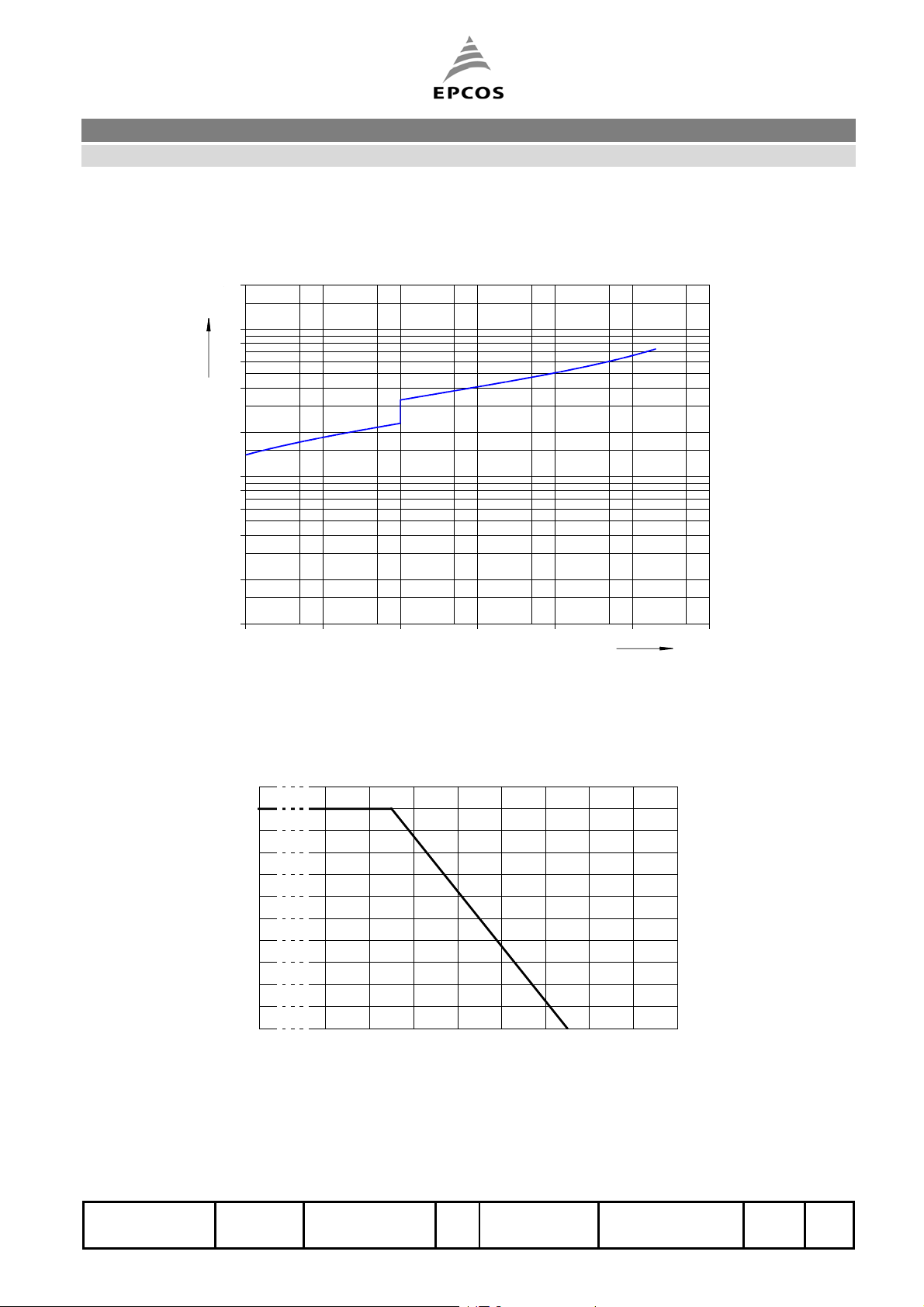
V-I-characteristic
200
200
V
v
100
80
60
40
20
10
8
6
4
2
1
-5
10
-4
10
-3
10
-2
10
-1
10
10
VAR9733A
0
101A
i
Max. current, energy and average power dissipation
depending on ambient temperature
%
100
90
80
70
60
50
40
30
20
10
0
-55 70 80 90 100 110 120 130 140 150 °
mbient temperature
ISSUE DATE 28.01.2005 ISSUE e PUBLISHER KB VS PE PAGE 2/7
Metal Oxide Varistors CT0402S14AHSG
SMD multilayer varistor with Ni-barrier termination B72590T8140S160
Electrical data
Maximum operating voltage
RMS voltage V
DC voltage VDC = 16 V
Varistor voltage (@ 1 mA) VV = 23 up to 33 V
Maximum clamping voltage (@ 1 A) VC = 66 V
Maximum average power dissipation P
Maximum surge current (8/20 µs) I
Maximum energy absorption (ESD) E
(@ ESD according to IEC 61000-4-2, 15 kV air discharge)
Capacitance (@ 1 MHz, 1V, 25 °C, typical value) C = 10 pF
= 14 V
RMS
= 3 mW
max
= 1 x 2 A
max
= 30 mJ
max
Response time < 0.5 ns
Operating temperature -40 … +85 °C
Storage temperature (mounted parts) -40 … +125 °C
Termination material Ag/Ni/Sn
Part weight 0.002 g
(thickness not specified, adjusted to fulfill wettability specification according to
IEC 60068-2-58)
Application note
The described component is designed to meet ESD level 4 requirements according to
IEC 61000-4-2 (8 kV contact discharge, 150 pF, 330 Ω)
ISSUE DATE 28.01.2005 ISSUE e PUBLISHER KB VS PE PAGE 3/7

Metal Oxide Varistors CT0402S14AHSG
SMD multilayer varistor with Ni-barrier termination B72590T8140S160
Signal insertion loss
-0.5
-1.5
-2.5
-3.5
insertion loss [dB]
-4.5
1)
0
-1
-2
-3
-4
-5
0 50 100 150 200 250 300
frequency [MHz]
1)
typical values, measured with network analyzer HP8753 E/S containing S-parameter test set.
Stability to multiple ESD discharges
40
30
20
10
0
0 1 10 100 1000 10000
2)
number of ESD pulses
2)
8 kV contact discharge, 150 pF, 330 Ω, according to IEC 61000-4-2.
ISSUE DATE 28.01.2005 ISSUE e PUBLISHER KB VS PE PAGE 4/7

Metal Oxide Varistors CT0402S14AHSG
SMD multilayer varistor with Ni-barrier termination B72590T8140S160
Recommended geometry of solder pad
B
C
B
A = 0.6 mm
B = 0.6 mm
A
A
C = 0.5 mm
E = 1.7 mm
D
Recommended soldering temperature profile
Soldering zone
max. 7 s
at max. temp.
Cooling-down zone
max. 2
(natural air cooling)
40 s
100 s
300
C
T
245
215
180
Preheating zone
C/s C/s
max. 2
100
20
0
50 100
150 200
250
s
t
VAR0543-W-E
This component should be soldered within 12 months after delivery from EPCOS. They
should be left in their original packings to avoid soldering problems due to oxidized terminals.
Storage temperature: -25 to 45 °C
Relative humidity: < 75% annual average, < 95% on maximum 30 days in a year.
The usage of mild non-activated fluxes for soldering is recommended, as well as proper
cleaning of the PCB.
The components are suited for Pb-free soldering.
ISSUE DATE 28.01.2005 ISSUE e PUBLISHER KB VS PE PAGE 5/7

Metal Oxide Varistors CT0402S14AHSG
g
y
SMD multilayer varistor with Ni-barrier termination B72590T8140S160
Taping according to IEC 60286-3
Tape material: cardboard
P
T
T
1
T
1
T
2
D
0
A
0
0
P
2
E
F
W
0
B
G
P
1
Direction of unreelin
Tape end (trailer)
Leader
Dimensions and tolerances:
Definition Symbol Dimension
[mm]
Compartment width A
Compartment length B
Sprocket hole diameter D
Sprocket hole pitch P
0
0
0
0
0.6 ± 0.2
1.15 ± 0.2
1.5 ± 0.1
4.0
Distance center hole to
center compartment
P
2
2.0 ± 0.05
Pitch of the component
compartments
P
1
2.0 ± 0.1
Tape width W 8.0 ± 0.3
Distance edge to center of
E 1.75 ± 0.1
hole
Distance center hole to
center compartment
Distance compartment to
F3.5± 0.05
G0.75min
edge
Thickness of cardboard tape T 0.6 max.
Overall thickness T
2
0.7 max.
Tolerance
± 0.1
40 min.
empty cavities
25 min.
empt
cavities
[mm]
1)
300 mm
cover tape
1)
£ ± 0.2 mm over any 10 pitches
ISSUE DATE 28.01.2005 ISSUE e PUBLISHER KB VS PE PAGE 6/7

Metal Oxide Varistors CT0402S14AHSG
SMD multilayer varistor with Ni-barrier termination B72590T8140S160
Packing
Each reel in airtight plastic bag with desiccant bag.
Dimensions approx. 220 x 220 mm. Weight approx. 170 g.
6 bags in cardboard box, dimensions approx. 250 x 220 x 130 mm. Weight approx. 1 kg.
Reel material: plastic
Packing unit: 10000 pcs./reel
Reel dimensions:
Definition Symbol Dimension
[mm]
Reel diameter A 180
Reel width
W
1
8.4
Tolerance
[mm]
+0/ -3
+1.5/ -0
(inside)
Reel width
W
2
14.4 max.
(outside)
Ó EPCOS AG 2005. Reproduction, publication and dissemination of this data sheet, enclosures hereto and the information
contained therein without EPCOS' prior express consent is prohibited.
Purchase orders are subject to the General Conditions for the Supply of Products and Services of the Electrical and
Electronics Industry recommended by the ZVEI (German Electrical and Electronic Manufacturers' Association), unless
otherwise agreed.
ISSUE DATE 28.01.2005 ISSUE e PUBLISHER KB VS PE PAGE 7/7
 Loading...