

Page 1

Development Board
EPC9058
Quick Start Guide
EPC2110
High Frequency Class-E Wireless Power Amplier
Revision 1.0
Page 2
QUICK START GUIDE
Demonstration System EPC9058
DESCRIPTION
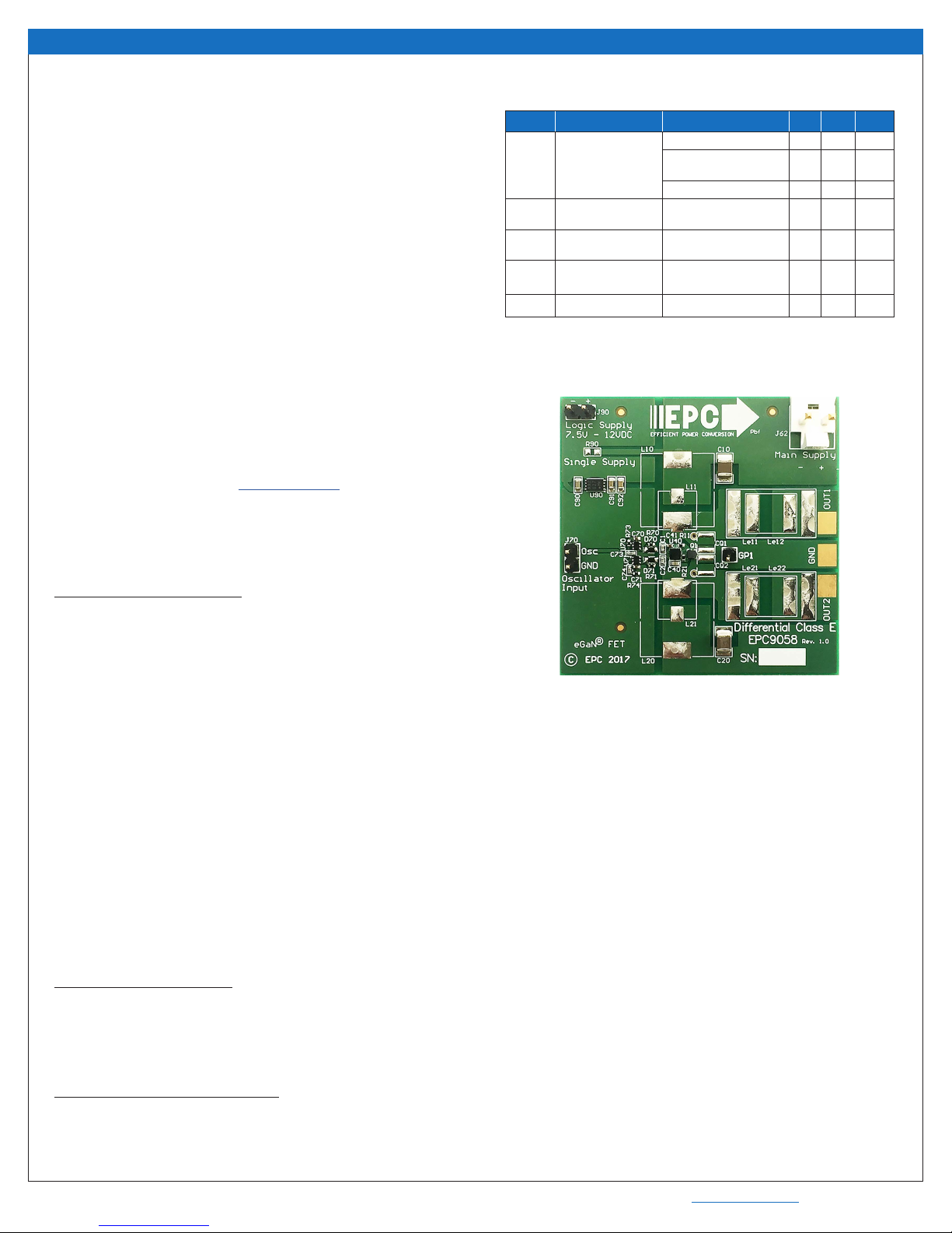
The EPC9058 is a high eciency, dierential mode Class-E amplier
development board that can operate up to 15 MHz, including 6.78 MHz
which is popular for wireless power. However, this board is not precongured for any particular frequency. The purpose of this development
board is to simplify the evaluation process of class-E amplier technology
using eGaN® FETs by allowing engineers to easily mount all the critical
class-E components on a single board that can be easily connected into
an existing system.
This board may also be used for applications where a low side switch is
utilized. Examples include, and are not limited to, push-pull converters,
current-mode Class D ampliers, common source bi-directional switch,
and generic high voltage narrow pulse width applications such as LiDAR.
The amplier board features the 120 V rated EPC2110 eGaN FET. The
amplier is set to operate in dierential mode and can be re-congured to
operate in single-ended mode and includes the gate driver and logic
supply regulator.
For more information on the EPC2110 eGaN FETs please refer to the
datasheet available from EPC at www.epc-co.com. The datasheet should
be read in conjunction with this quick start guide.
Table 1: Performance Summary (TA = 25°C) EPC9058
Symbol Parameter Conditions Min Max Units
Class-E Conguration 0 20 V
Main Supply Voltage
V
IN
V
DD
I
OUT
V
OSC
* Maximum current depends on die temperature – actual maximum current will be subject to switching
frequency, bus voltage and thermals.
Range
Control Supply Input
Range
Switch Node Output
Current (each)
Oscillator Input
Threshold
Current Mode Class-D
Conguration
Push-Pull Conguration 0 52 V
Input ‘Low’ -0.3 1.5 V
Input ‘High’ 3.5 5 V
0 20 V
7 12 V
2* A
DETAILED DESCRIPTION
The Amplier Board (EPC9058)
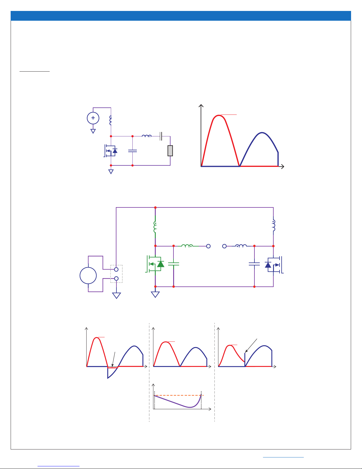
Figure 1 shows the schematic of a single-ended, Class-E amplier with
ideal operation waveforms where the amplier is connected to a tuned
load such as a highly resonant wireless power coil. The amplier has not
been congure due to the specic design requirements such as load resistance and operating frequency. The design equations of the specic ClassE amplier support components are given in this guide and specic values
suitable for a RF amplier application can then be calculated.
Figure 2 shows the dierential mode Class-E amplier EPC9058 demo board
power circuit schematic. In this mode the output is connected between
Out 1 and Out 2. A block-wave external oscillator with 50 % duty cycle and
0 V – 5 V signal amplitude is used as a signal for the board. Duty cycle
modulation is recommended only for advanced users who are familiar with
the Class-E amplier operation and require additional eciency.
The EPC9058 is also provided with a 5 V regulator to supply power
to the logic circutis and gate driver. Adding a 0 Ω resistor in position
R90 allows the EPC9058 to be powered using a single-supply
voltage; however in this conguration the maximum operating voltage
is limited to between 7 V and 12 V.
Single-ended Mode operation
Although the default conguration is dierential mode, the demo board
can be re-configured for single-ended operation by shorting out
C74 (which disables only the drive circuit) and connecting the
load between Out 1 and GND only (see gures 2 and 5 for details).
Class-E amplier operating limitations
The impact of load resistance variation is signicant to the performance of
the Class-E amplier, and must be carefully analyzed to select the optimal
design resistance.
EPC9058 amplier board.
The impact of load resistance (R
– Real part of Z
Load
) variation on the
Load
operation of the Class-E amplier is shown in gure 3. When operating
a Class-E amplier with a load resistance (R
– Real part of Z
Load
Load
)
that is below the design value (see the waveform on the left of
gure 3), the load tends to draw current from the amplier too
quickly. To compensate for this condition, the amplier supply
voltage is increased to yield the required output power. The shorter
duration of the energy charge cycle leads to a signicant increase in
the voltage to which the switching device is exposed. This is done
in order to capture sucient energy and results in device body
diode conduction during the remainder of the device o period.
This period is characterized by a linear increase in device losses as a
function of decreasing load resistance (R
When operating the Class-E amplier with a load resistance (R
Load
).
) that
Load
is above the design value (see the waveform on the right of gure 3), the
load tends to draw insucient current from the amplier, resulting in an
incomplete voltage transition. When the device switches there is a
residual voltage across the device, which leads to shunt capacitance
(C
+ Csh) losses. This period in the cycle is characterized by an expo-
OSS
nential increase in device losses as function of increasing reected load
resistance.
2 | | EPC – EFFICIENT POWER CONVERSION CORPORATION | WWW.EPC-CO.COM | COPYRIGHT 2017
Page 3

QUICK START GUIDE
Demonstration System EPC9058
Given these two extremes of the operating load resistance (R
Load
), the
optimal point between them must be determined. In this case, the
optimal point yields the same device losses for each of the extreme load
resistance points and is shown in the lower center graph of gure 3. This
optimal design point can be found through trial and error, or using circuit
simulation.
Class-E amplier design
For this amplier only three components need to be specically
designed; 1) the extra inductor (Le), 2) the shunt capacitor (Csh) and, 3) the
selection of a suitable switching device. The RF choke (L
) value is less
RFck
critical and hence can be chosen or designed.
The design equations for the Class-E amplier have been derived by
N. Sokal [1]. To simplify these equations, the value of QL in [1] is set to
innity, which is a reasonable approximation in most applications within
the frequency capability of this development board. The design needs to
have a specic load resistance (R
) value and desired load power (P
Load
Load
)
that is used to begin the design, which then drives the values of the other
components, including the magnitude of the supply voltage.
The Class-E amplier passive component design starts with the load
impedance value (Z
) shown in gure 1. The reactive component of Z
Load
Load
is tuned out using a series capacitor CS, which also serves as a DC block,
resulting in R
. It is a common mistake to ignore the need for the DC
Load
block, where a failure to do so can yield a DC current from the supply
through to the load, and lead to additional losses in several components
in that path.
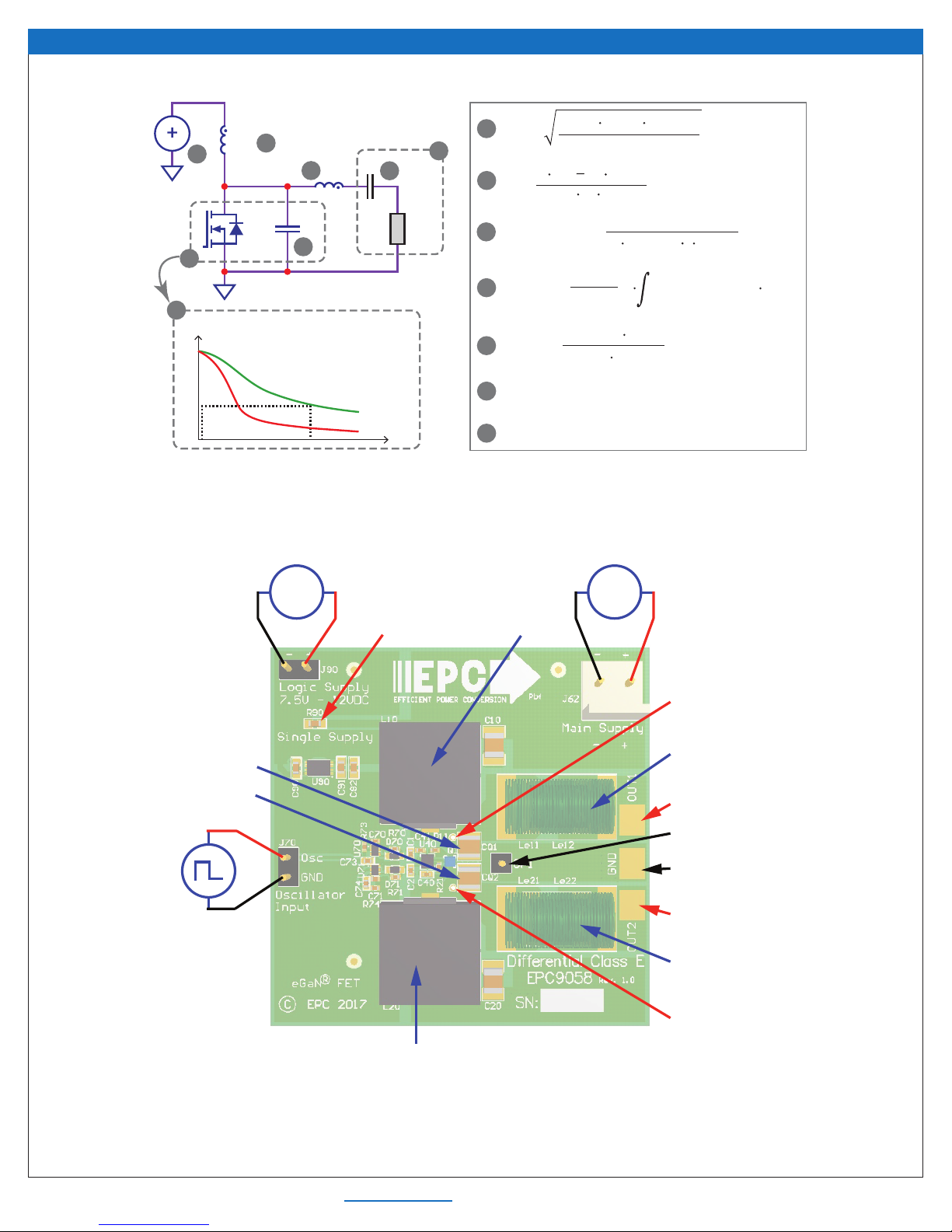
First, using the equations in gure 4, both the extra inductor
Le (equation 2 and shunt capacitor (equation 3) values can be
determined [2], [3]. The value of the shunt capacitor includes the
C
of the switching device, which must be subtracted from the
OSS
calculated value to yield the actual external capacitor (Csh) value. To
do this, rst the magnitude of the supply voltage (VDD) is calculated
using equation 1, which in turn can be used to determine the peak
device voltage (3.56 · VDD).
The RMS value of the peak device voltage is then used to determine the
C
of the device at that voltage. This is the capacitance that will be
OSSQ
deducted from the calculated shunt capacitor to reveal the external
shunt capacitor (Csh) value. The C
integrating the C
C
value is larger than the calculated shunt capacitance, the design
OSSQ
as function of voltage using equation 4. If the
OSS
of the device can be calculated by
OSSQ
cannot be realized for the load resistance specied and a new load
resistance (R
Finally, the choke (L
) must be chosen.
Load
) can be designed using equation 5 and, in this case,
RFck
a minimum value is specied. Larger values yield lower ripple current,
which can lead to a more stable operating amplier. A too-low value will
lead to increased operating losses and change the mode of operation of the
amplier. In some cases this can be intentional.
Here:
R
= Load Resistance [Ω]
Load
P
= Load Power [W]
Load
VDD = Amplier Supply Voltage [V]
f = Operating Frequency [Hz]
Le = Extra Inductor [H]
Csh = Shunt Capacitor [F]
C
= Output Capacitance of the FET [F]
OSS
C
= Charge Equivalent Device Output Capacitance [F]
OSSQ
(See gure 6 of the EPC2110 datasheet)
VDS = Drain-Source Voltage of the FET [V]
L
= RF Choke Inductor [H]
RFck
CS = Series Tuning Capacitor [F]
Z
= Load Impedance [Ω]
Load
NOTE. For dierential mode amplier design details, please refer to the
application note ‘AN021: eGaN FETs for Low Cost Resonant Wireless
Power Applications’
[1] N.O. Sokal, “Class-E RF Power Ampliers,” QEX, Issue 204, pp. 9–20,
January/ February 2001.
[2] M. Kazimierczuk, “Collector amplitude modulation of the Class-E
tuned power amplier,” IEEE Transactions on Circuits and Systems,
June 1984, Vol.31, No. 6, pp. 543–549.
[3] Z. Xu, H. Lv, Y. Zhang, Y. Zhang, “Analysis and Design of Class-E Power
Amplier employing SiC MESFETs,“ IEEE International Conference on
Electron Devices and Solid-State Circuits (EDSSC) 2009, 25–27
December 2009, pp 28–31.
QUICK START PROCEDURE
The EPC9058 amplier board is easy to set up to evaluate the
performance of the eGaN FET in a class-E amplier application. Once
the design of the passive components has been completed and
installed, then the board can be powered up and tested.
1. Make sure the entire system is fully assembled prior to making
electrical connections including an applicable load.
2. With power o, connect the main input power supply bus to J62
as shown in gure 5. Note the polarity of the supply connector.
Set the voltage to 0 V.
3. With power o, connect the logic input power supply bus to J90
as shown in gure 5. Note the polarity of the supply connector.
Set the voltage to between 7 V and 12 V.
4. Make sure all instrumentation is connected to the system.
This includes the external oscillator to control the circuit.
5. Turn on the logic supply voltage.
6. Turn on the main supply voltage starting from 0 V, and increase
to the desired value. Note operating conditions and in particular
the thermal performance and voltage of the FETs to prevent overtemperature and over-voltage failure.
7. Once operation has been conrmed, observe the device voltage,
eciency and other parameters on both the amplier and
device boards.
8. For shutdown, please follow steps in the reverse order.
EPC – EFFICIENT POWER CONVERSION CORPORATION | WWW.EPC-CO.COM | COPYRIGHT 2017 | | 3
Page 4
QUICK START GUIDE
Capacitance
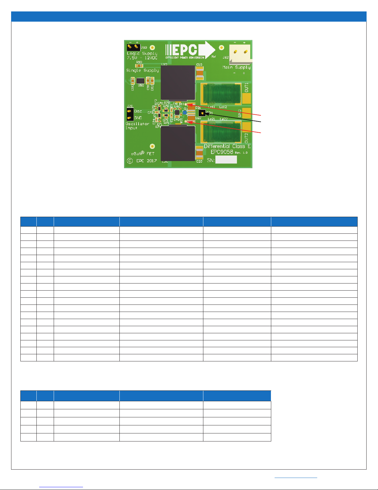
NOTE. When measuring the high frequency content switch-node, care must be taken
to avoid long ground leads. An oscilloscope probe connection (preferred method) has
been built into the board to simplify the measurement of the Drain-Source Voltage
(shown in gure 6). The choice of oscilloscope probe needs to consider tip capacitance
where this will appear in parallel with the shunt capacitance thereby altering the operating
point of the amplier.
Pre-Cautions
The EPC9058 development board showcases the EPC2110 eGaN FETs in
a class-E amplier application. Although the electrical performance
surpasses that of traditional silicon devices, their relatively smaller size
does require attention paid to thermal management techniques.
V
DD
L
RFck
C
S
L
e
Demonstration System EPC9058
The EPC9058 development board has no current or thermal protection
and care must be exercised not to over-current or over-temperature
the devices. Excessively wide load impedance range variations can lead
to increased losses in the devices. The operator must observe the
temperature of the gate driver and eGaN FETs to ensure that both are
operating within the thermal limits as per the datasheets. Always check
operating conditions and monitor the temperature of the EPC devices
using an IR camera.
V / I
3.56 x V
DD
V
C
sh
Q
1
Z
Load
DS
50%
I
D
Time
Ideal waveforms
Figure 1: Single-ended, Class-E amplier with ideal operation waveforms.
L
RFck1
L
V
IN
+
J1
Q
1
e1x
C
CQ1
Coil connection
L
e2x
C
CQ2
L
RFck2
Q
2
Figure 2: EPC9058 power circuit schematic.
~6.5 x V
Body diode
V / IV / I
DD
3.56 x V
DD
V / I
~2 x V
(C
+ Csh)
OSS
losses
DD
conduction
V
DS
50%
I
D
V
DS
P
FETloss
50%
I
D
Time TimeTime
V
DS
50%
I
D
Optimal design
R
Load_Design
R
< Design point
Load
Drives FET voltage rating
= Design point
R
Load
R
Load
Figure 3: Class-E operation under various load conditions that can be used to determine the optimal design load resistance (R
> Design point
R
Load
Drives FET C
OSS
choice
).
load
4 | | EPC – EFFICIENT POWER CONVERSION CORPORATION | WWW.EPC-CO.COM | COPYRIGHT 2017
Page 5
QUICK START GUIDE
V
Demonstration System EPC9058
1
4
4
Capacitance
DD
1
2
3
4
5
6
7
VDD =
π (π
L
=
e
C
+ C
OSSQ
C
= C
OSSQ
L
RFck
>
DC Block
R
Load
L
5
RFck
C
Q
OSS
C
S
L
2
e
C
sh
C
3
OSSQ
1
6
Voltage
7
Z
Load
P
R
Load
2
4)
32 π f
=
sh
1
V
DD
2
+ 4)
(π
π
4 f
Load
8
R
Load
2
(π
R
(π2 + 4)
4
2
+ 4)
f R
V
DD
0
Load
OSS
Load
(VDS)
dv
DS
Figure 4: Class-E amplier design process with equations.
7 V - 12 VDC
supply
V
Logic
(note polarity)
+
Single supply jumper
RF choke 1
+
0 V - 20 V
DCmax
VIN supply
(note polarity)
Out A oscilloscope probe
L
C
Sh1
C
Sh2
e1
Output 1 pad
Ground post
Ground pad output
External oscillator
Output 2 pad
L
e2
Out B oscilloscope probe
RF Choke 2
Figure 5: Proper connection and measurement setup for the amplier board.
EPC – EFFICIENT POWER CONVERSION CORPORATION | WWW.EPC-CO.COM | COPYRIGHT 2017 | | 5
Page 6
QUICK START GUIDE
Demonstration System EPC9058
Figure 6: Proper measurement of the drain voltage.
Table 2: EPC9058 Bill of Materials
Item Qty Reference Part Description Manufacturer Part #
1 4 C1, C2, C73, C74 22 pF, 50 V Würth 885012005057
2 2 C10, C20 2.2 µF 100 V Taiyo Yuden HMK325B7225KN-T
3 1 C40 4.7 µF, 10 V Samsung CL05A475MP5NRNC
4 3 C41, C70, C71 100 nF, 16 V Würth 885012205037
5 3 C90, C91, C92 1 µF, 25 V Würth 885012206076
6 2 D70, D71 40 V 30 mA Diodes Inc. SDM03U40
7 1 GP1 .1" Male Vert. Würth 61300111121
8 1 J62 .156" Male Vert. Würth 645002114822
9 2 J70, J90 .1" Male Vert. Würth 61300211121
10 1 Q1 120 V, 3.4 A, 60 mΩ EPC EPC2110
11 2 R11, R21 2.2 Ω Yageo RC0402JR-072R2L
12 2 R70, R71 0 Ω Samsung RC1005J000CS
13 1 R73 10 kΩ Yageo RC0402FR-0710KL
14 1 R74 10 kΩ Panasonic ERJ-2GEJ103X
15 1 R90 0 Ω (EMPTY ) Stackpole RMCF0603ZT0R00
16 1 U40 100 V eGaN Driver Texas Instruments LM5113TM
17 1 U70 2 In NAND Fairchild NC7SZ00L6X
18 1 U71 2 In AND Fairchild NC7SZ08L6X
19 1 U90 5.0 V 250 mA DFN Microchip MCP1703T-5002E/MC
Table 3: Optional Components
Item Qty Reference Part Description Manufacturer
1 2 CQ1, CQ2 Capacitor size 1111 Designed for Johanson
2 2 L10, L20 Inductor 13 x 13 mm Designed for Würth
3 2 L11, L21 Inductor 6.9 x 6.9 mm Designed for Würth
4 2 Le11, Le21 Coil size 2929SQ Designed for CoilCraft
5 2 Le12, Le22 Coil size 2222SQ Designed for CoilCraft
6 | | EPC – EFFICIENT POWER CONVERSION CORPORATION | WWW.EPC-CO.COM | COPYRIGHT 2017
Page 7
QUICK START GUIDE
EPC – EFFICIENT POWER CONVERSION CORPORATION | WWW.EPC-CO.COM | COPYRIGHT 2017 | | 7
Demonstration System EPC9058
Vsup
7.5VDC
- 12VDC
Logic Supply Regulator
V7in
Vsup
Main Supply
Vsup
2.2 Ω
2.2 Ω
1 2
R11
1 2
R21
GRH
GRL
5V
5 V
5 V
5 V
GLH
GLL
Gate Driver
U40
LM5113TM
L_Sig
R_Sig
LOGIC
SDM03U40
40 V, 30 mA
D71
5 V
5 V
5 V
Deadtime Left
Deadtime Right
Oscillator input
A
B
U70
NC7SZ00L6X
5 V
OSC
GRH GRL
GL L
GLH
TBD
L10
TBD
L20
OSC
OSC
OSC
Logic
Supply
Vsup
Vsup
Vsup
Single Supply Conguration
TBD
CQ2
TBD
CQ1
V7in
OutA
OutB
2.2 μF, 100 V
C20
2.2 μF , 100 V
C10
TBD
Le11
TBD
Le12
TBD
Le21
TBD
Le22
TBD
L21
SDM03U40
40 V, 30 mA
D70
A
B
Y
U71
NC7SZ00L6X
0 Ω
0 Ω
1 2
R90
Out1
Out2
GND
.1" Male Vert.
1
2
J90
5VV7in
MCP1703T-5002E/MC
5.0 V 250 mA DFN
OUT
GN DINGN D
U90
nSD
nSD
5 V
10 k
1
2
R74
.1" Male Vert.
1
2
J70
4.7 μF, 10 V
C40
1 2
R70
1 2
R71
10 k
1
2
R73
1
.1" Male Vert.
GP1
Ground Post
1
ProbeHole
PH1
1
ProbeHole
PH2
1
2
.156" Male Vert.
J62
100 nF, 16 V
C70
100 nF, 16 V
C71
100 nF, 16 V
C41
22 pF, 50 V
C1
22 pF, 50 V
C2
22 pF, 50 V
C73
22 pF, 50 V
C74
1 μF, 25 V
C90
1 μF, 25 V
C91
1 μF, 25 V
C92
Q1
EPC2110
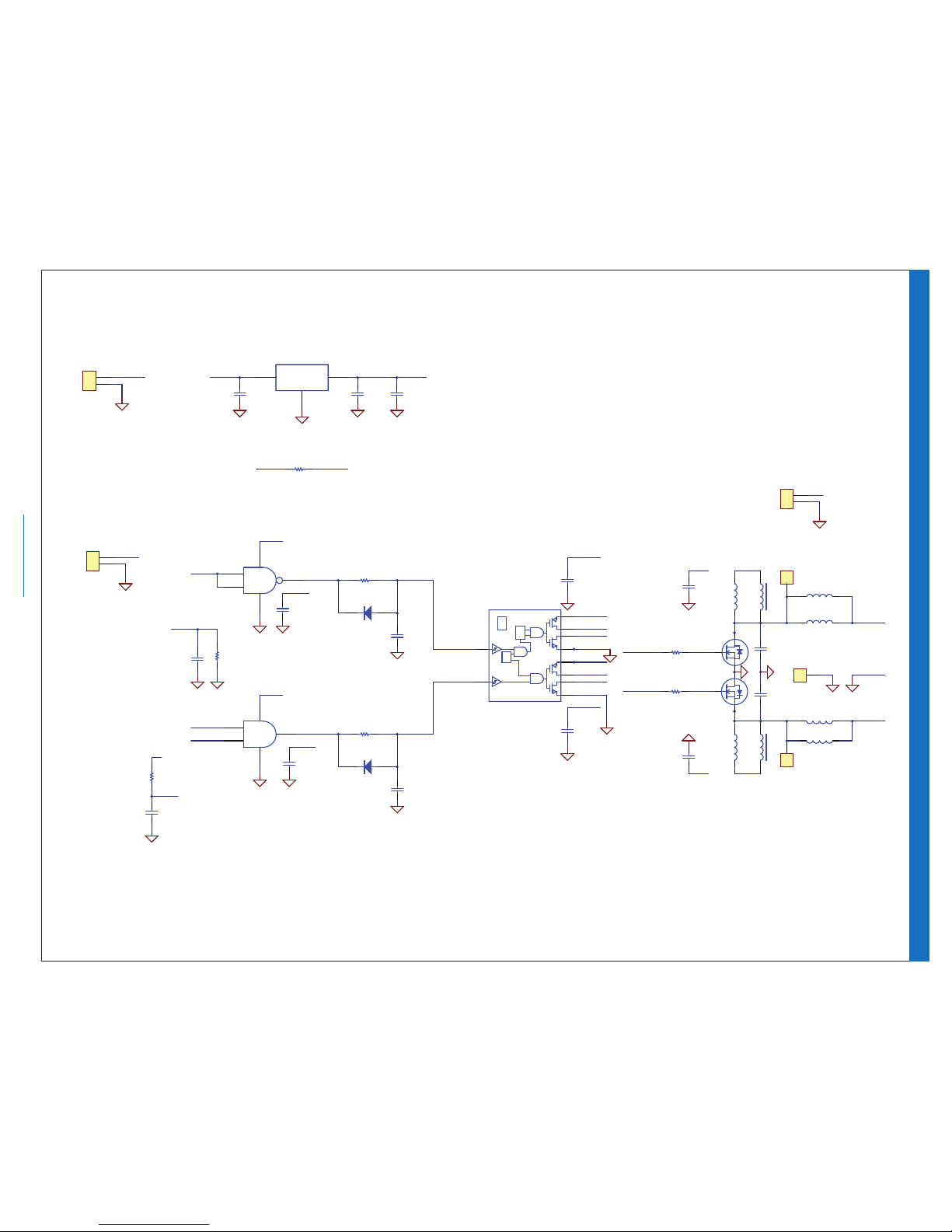
Figure 7: EPC9058 Class-E amplier schematic.
Page 8

For More Information:
Please contact [email protected]
or your local sales representative
Visit our website:
www.epc-co.com
Sign-up to receive
EPC updates at
bit.ly/EPCupdates
or text “EPC” to 22828
EPC Products are distributed through Digi-Key.
www.digikey.com
Demonstration Board Warning and Disclaimer
The EPC9058 board is intended for product evaluation purposes only and is not intended for commercial use. Replace components on the Evaluation Board only with those parts shown on
the parts list (or Bill of Materials) in the Quick Start Guide. Contact an authorized EPC representative with any questions.
This board is intended to be used by certied professionals, in a lab environment, following proper safety procedures. Use at your own risk.
As an evaluation tool, this board is not designed for compliance with the European Union directive on electromagnetic compatibility or any other such directives or regulations. As board
builds are at times subject to product availability, it is possible that boards may contain components or assembly materials that are not RoHS compliant. Ecient Power Conversion
Corporation (EPC) makes no guarantee that the purchased board is 100% RoHS compliant.
The Evaluation board (or kit) is for demonstration purposes only and neither the Board nor this Quick Start Guide constitute a sales contract or create any kind of warranty, whether express
or implied, as to the applications or products involved.
Disclaimer: EPC reserves the right at any time, without notice, to make changes to any products described herein to improve reliability, function, or design. EPC does not assume any liability
arising out of the application or use of any product or circuit described herein; neither does it convey any license under its patent rights, or other intellectual property whatsoever, nor the
rights of others.
 Loading...