

Page 1

Polmaddie6 User Manual
Issue – 2.2
Page 2

© Enterpoint Ltd. – Polmaddie6 Manual – Issue 2.2 05/05/2017
2
Foreword
PLEASE READ THIS ENTIRE MANUAL BEFORE PLUGGING IN
OR POWERING UP YOUR POLMADDIE6 BOARD.
PLEASE TAKE SPECIAL NOTE OF THE WARNINGS WITHIN
THIS MANUAL.
Trademarks
Altera, Quartus II, Max10 and NIOS are the registered trademarks of Altera Inc, San Jose,
California, US.
Polmaddie6 is a trademark of Enterpoint Ltd.
Page 3
© Enterpoint Ltd. – Polmaddie6 Manual – Issue 2.2 05/05/2017
3
CONTENTS
Foreword
2
Trademarks
2
Introduction
4
Polmaddie6 Features
5
Getting Started
6
Polmaddie Features
7
Power Input
7
Io Headers
8
FPGA
10
Oscillator
10
Leds
11
Switches
12
USB Interface
13
Programming Polmaddie6
14
Mechanical Arrangement
15
Medical and Safety Critical Use
16
Warranty
16
Support
16
Page 4
© Enterpoint Ltd. – Polmaddie6 Manual – Issue 2.2 05/05/2017
4
Introduction
Welcome to your Polmaddie6 board. Polmaddie is Enterpoint’s low cost product range that offers
an economical way to begin programming with CPLDs and FPGAs.
Polmaddie6 features Altera’s low cost MAX10, which is highly flexible and facilitates development
of simple microprocessor systems based on Altera’s NIOS processor.
The aim of this manual is to assist in using the main features of Polmaddie6.
The Polmaddie6 board comes in several variants based on different devices. Polmaddie6 is based
on an Altera Max10 10M08SAE144C8G FPGA. Should you require a board based on another
member of the MAX10 family:
http://www.altera.com/literature/br/br-max10-brochure.pdf?GSA_pos=6&WT.oss_r=1&WT.oss=max10
please contact Enterpoint sales for a quote.
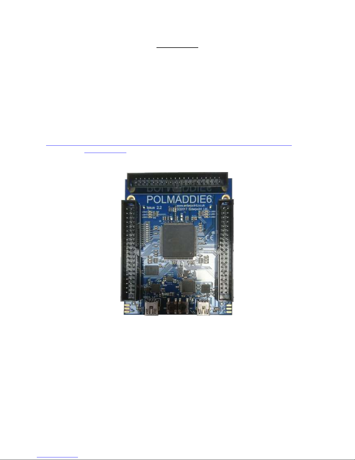
Figure 1 – Polmaddie6 Board
Page 5
© Enterpoint Ltd. – Polmaddie6 Manual – Issue 2.2 05/05/2017
5
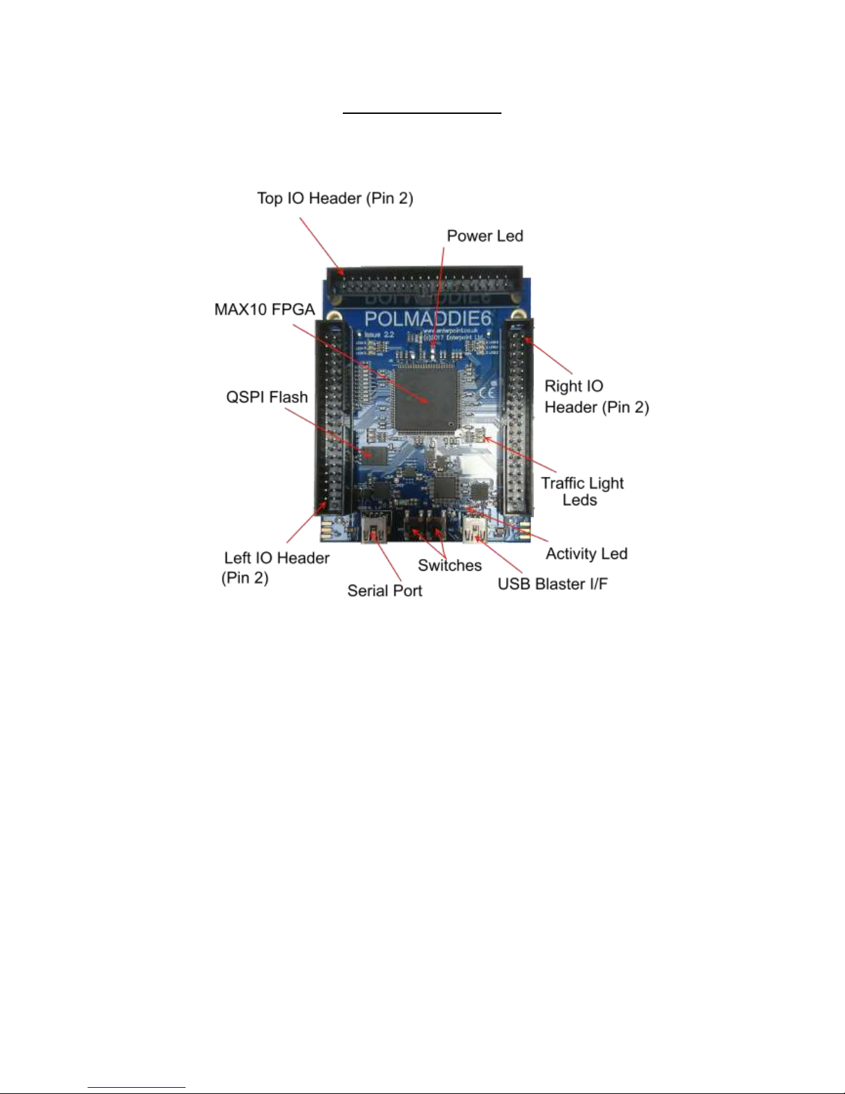
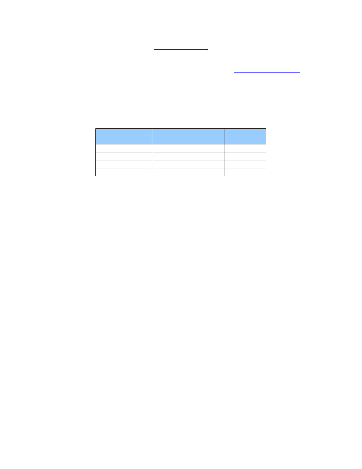
Polmaddie6 features
Figure 2 – Polmaddie6 Features
Page 6

© Enterpoint Ltd. – Polmaddie6 Manual – Issue 2.2 05/05/2017
6
Getting Started
Your Polmaddie6 will be supplied pre-programmed with a ‘traffic lights’ test design. The test
design will allow the user to determine that the LEDs and the push button switches of the
Polmaddie6 board are working. To use this test you should:
(1) Apply power to the Polmaddie6 board by plugging a cable into either of the USB sockets from a
USB power supply adapter or a PC Cable.
(2) The LEDs should light in a ‘traffic lights’ sequence. There is also Power indicator LED which
will light to show that power is present and the 3.3V regulator is working.
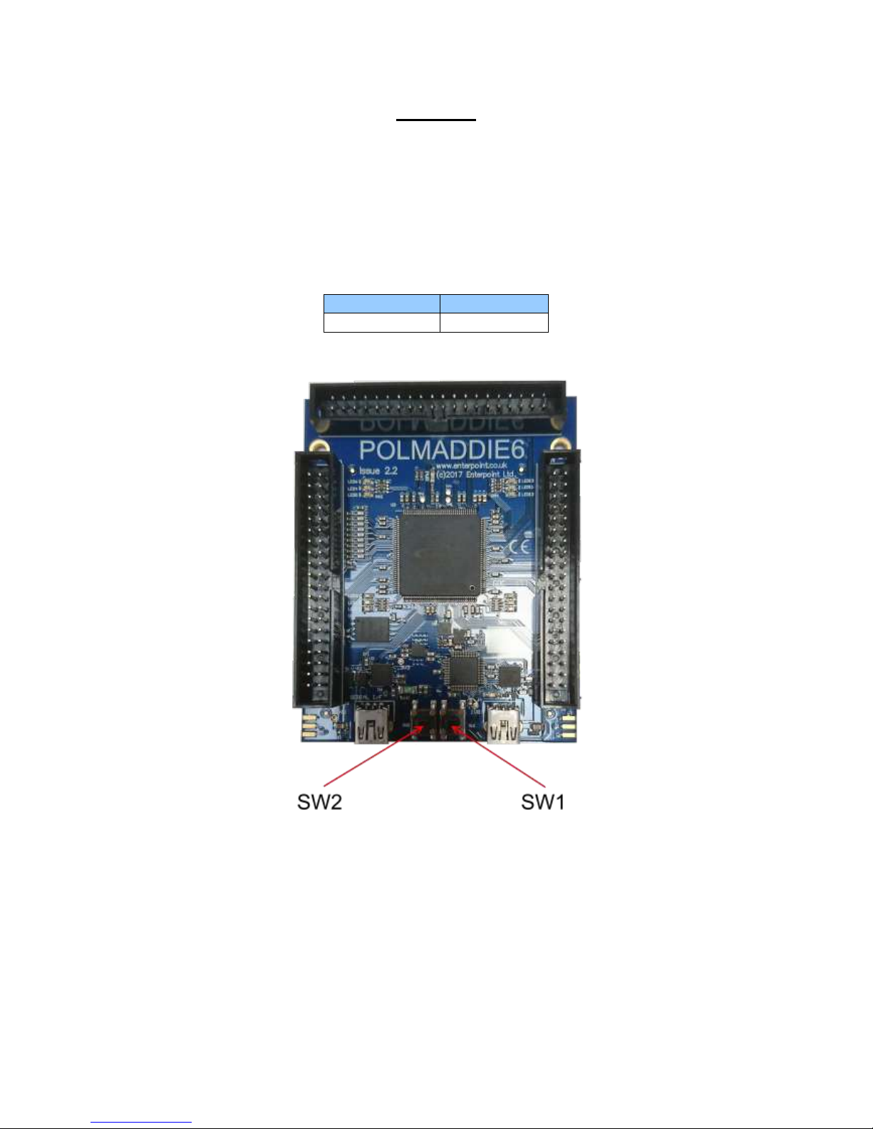
(3) Press SW2 (This is the left Push Button switch). The traffic lights sequence will be held in reset
until the switch is released.
(4) Press SW1 (This is the right Push Button switch). The traffic lights sequence will be held in
reset until the switch is released.
Page 7
© Enterpoint Ltd. – Polmaddie6 Manual – Issue 2.2 05/05/2017
7
Power Input
Polmaddie6 is powered by plugging a cable into the either of the USB sockets. The power can be
either from a USB power supply adapter or a PC.
The USB 5V supply is used to power the USB interface and to supply a voltage regulator producing
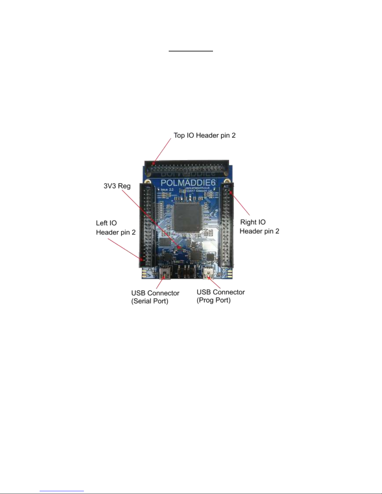
3.3V to power the FPGA, the LEDs and the oscillator. 3.3V is also available on pin 2 of each of the
IO headers. If you decide to use this as a source of power for external circuitry please remember
that the maximum total power available from the 3.3V Regulator is 1.2 Amps.
Figure 3 – Polmaddie6 Power Supply Features.
WARNING – THE REGULATORS MAY BECOME HOT IN NORMAL
OPERATION ALONG WITH THE BOARDS THERMAL RELIEF. PLEASE
DO NOT TOUCH OR PLACE HIGHLY FLAMABLE MATERIALS NEAR
THESE DEVICES WHILST THE POLMADDIE6 BOARD IS IN
OPERATION.
Page 8
© Enterpoint Ltd. – Polmaddie6 Manual – Issue 2.2 05/05/2017
8
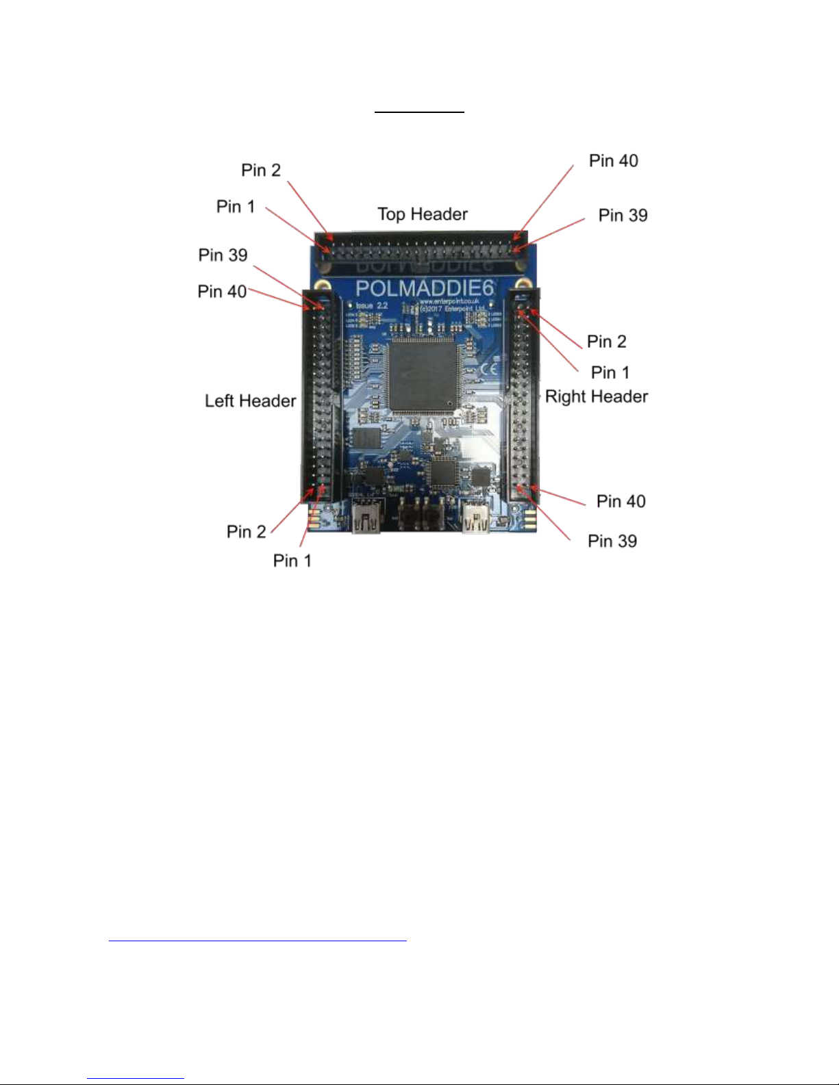
IO Headers
Figure 4 – Polmaddie6 Headers
The three 40-pin IDC Headers provide a simple mechanical and electrical interface for external
signal inputs. The connectors on this header are on a 0.1inch (2.54mm), pitch and allow other
electronic circuitry or user-designed add-on boards to be connected.
The headers each have 20 IOs routed to the FPGA. These are NOT 5V tolerant, the maximum
input voltage should be limited to 3.3V. IO21 is a dedicated Analog input. All the other IO can be
used as digital inputs or outputs. The headers each also have a permanent positive power pin on pin
2 and 19 permanent 0V connections as shown below:
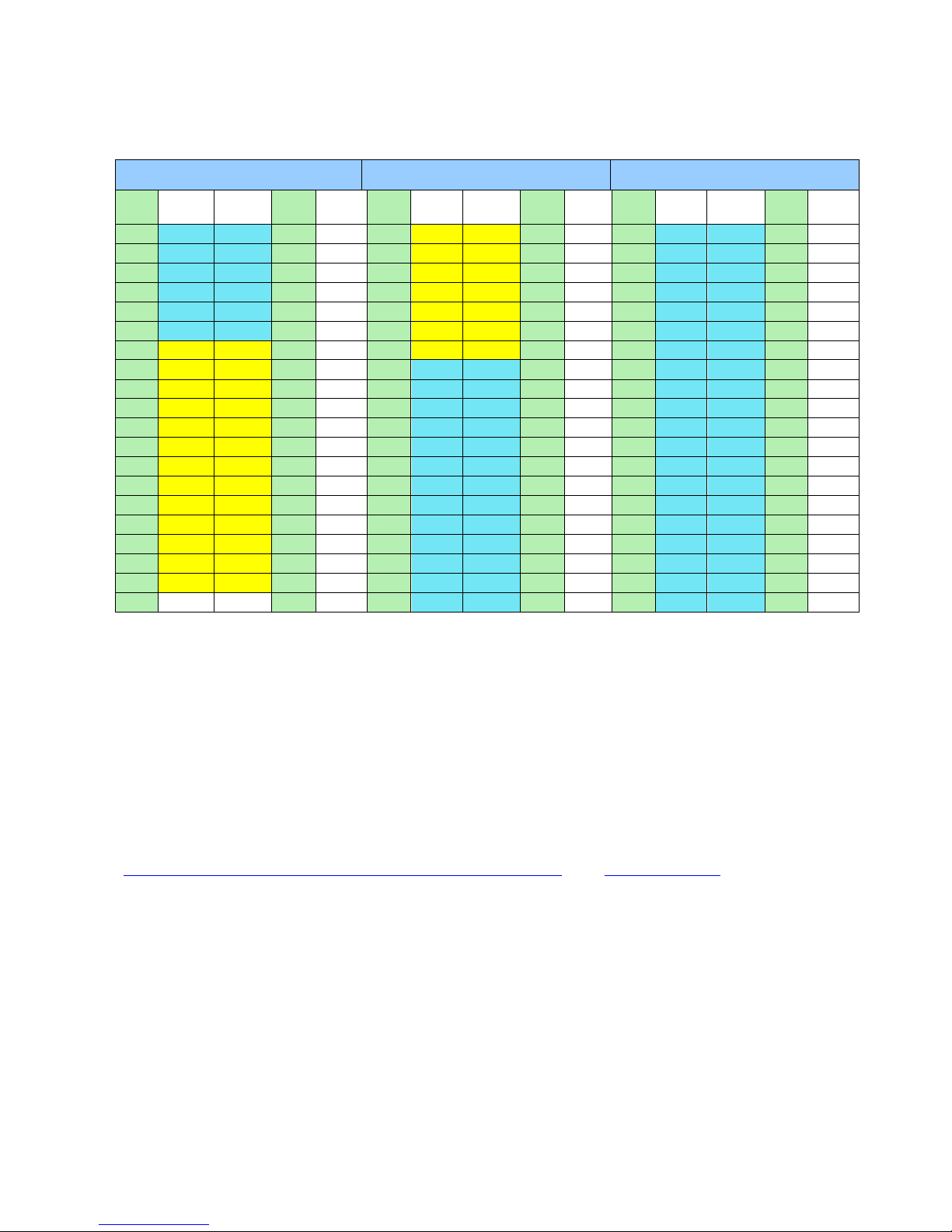
Digital IO
Max10 digital IO are either High Speed or Low Speed. In the table below High Speed IO are shown
shaded blue (pins 26 to 119) and Low Speed IO are shaded yellow (pins 6-25 and 120-132). More
information about the IO specifications and capabilities is available .
http://www.altera.co.uk/literature/lit-max-10.jsp
Page 9
© Enterpoint Ltd. – Polmaddie6 Manual – Issue 2.2 05/05/2017
9
LEFT HEADER
TOP HEADER
RIGHT HEADER
PIN
USE
FPGA
PIN
PIN
USE
PIN
USE
FPGA
PIN
PIN
USE
PIN
USE
FPGA
PIN
PIN
USE
1
IO40
33 2 3.3V
1
IO20
132
2
3.3V
1
IO60
93 2 3.3V
3
IO39
32 4 0V 3 IO19
131 4 0V 3 IO59
92 4 0V 5 IO38
30 6 0V 5 IO18
130 6 0V 5 IO58
91 6 0V 7 IO37
29 8 0V 7 IO17
127 8 0V 7 IO57
90 8 0V
9
IO36
28
10
0V 9 IO16
124
10
0V 9 IO56
89
10
0V
11
IO35
26
12
0V
11
IO15
123
12
0V
11
IO55
87
12
0V
13
IO34
25
14
0V
13
IO14
120
14
0V
13
IO54
86
14
0V
15
IO33
24
16
0V
15
IO13
119
16
0V
15
IO53
85
16
0V
17
IO32
22
18
0V
17
IO12
118
18
0V
17
IO52
84
18
0V
19
IO31
21
20
0V
19
IO11
114
20
0V
19
IO51
81
20
0V
21
IO30
17
22
0V
21
IO10
113
22
0V
21
IO50
80
22
0V
23
IO29*
14
24
0V
23
IO9
112
24
0V
23
IO49
79
24
0V
25
IO28*
13
26
0V
25
IO8
111
26
0V
25
IO48
78
26
0V
27
IO27*
12
28
0V
27
IO7
110
28
0V
27
IO47
77
28
0V
29
IO26*
11
30
0V
29
IO6
106
30
0V
29
IO46
76
30
0V
31
IO25*
10
32
0V
31
IO5
100
32
0V
31
IO45
69
32
0V
33
IO24*
8
34
0V
33
IO4
99
34
0V
33
IO44
66
34
0V
35
IO23*
7
36
0V
35
IO3
98
36
0V
35
IO43
65
36
0V
37
IO22*
6
38
0V
37
IO2
97
38
0V
37
IO42
64
38
0V
39
IO21*
3
40
0V
39
IO1
96
40
0V
39
IO41
62
40
0V
*these signals have series 470 resistors and 10pf capacitors to ground so they can be used as analog
inputs.
Analog Inputs
The Max10 device has one dedicated analog input (IO21) and eight optional analog/digital IO.
When they are used for analog signals IO 22 to 29 are single ended inputs connecting to a 12 bit
ADC with a maximum sampling rate of 1MHz. The maximum input voltage is 3.3V. More
information about the Max10 analog capability can be found in
http://www.altera.co.uk/literature/hb/max-10/ug_m10_adc.pdf from www.altera.com.
Page 10
© Enterpoint Ltd. – Polmaddie6 Manual – Issue 2.2 05/05/2017
10
FPGA
The main device on the Polmaddie6 is the Altera Max10 10M08SAE144C8G FPGA. Device
documentation can be obtained from:
http://www.altera.co.uk/literature/lit-max-10.jsp
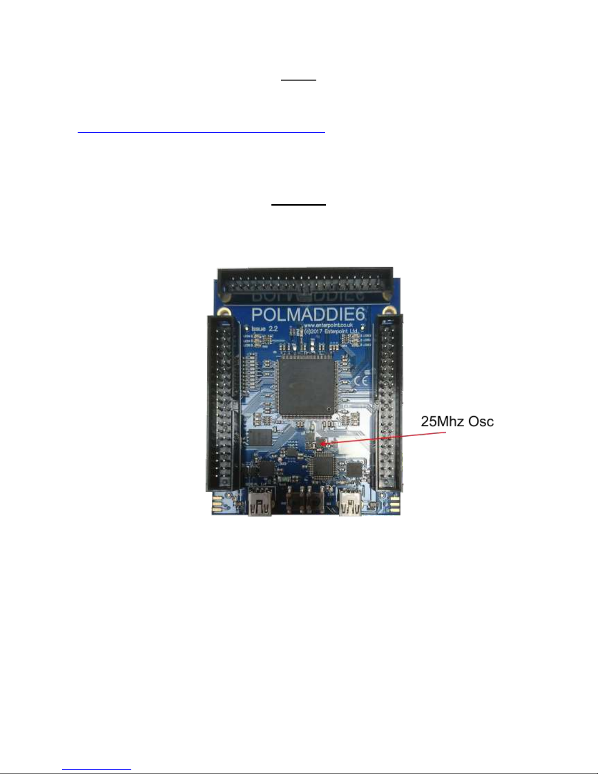
Oscillator
The oscillator on Polmaddie6 is a 3.3V, 25MHz ASEM oscillator. This clock signal is routed
through the MAX V CPLD to the FPGA on Pin 88, which is a clock input.
Figure 5 – Polmaddie6 Oscillator
Page 11
© Enterpoint Ltd. – Polmaddie6 Manual – Issue 2.2 05/05/2017
11
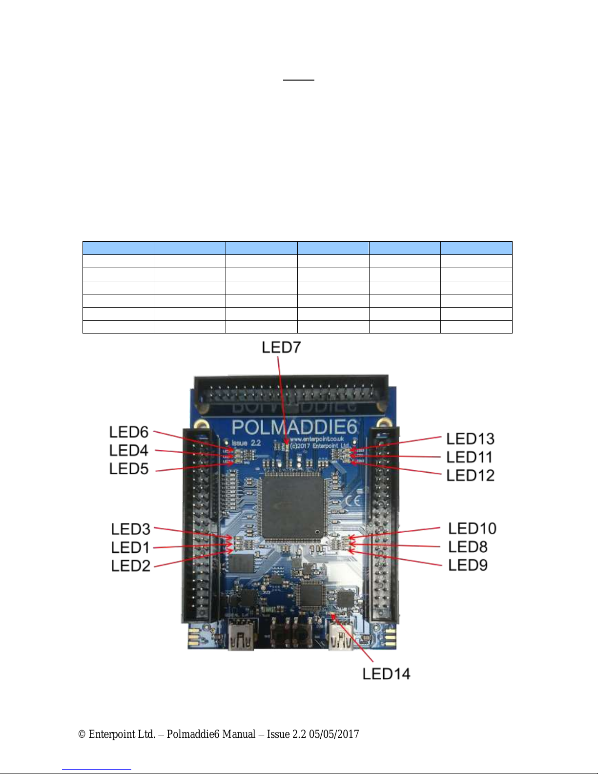
LEDs
Polmaddie6 has 14 LEDs.
LED 7 is a green power indicator LED and indicates the presence of the 3.3V supply. It cannot be
controlled by the FPGA.
LED 14 is a green Programming I/F Activity LED which is controlled by the MAX V CPLD. I t
cannot be controlled by the FPGA.
LEDs 1 to 6 and 8 to 13 are arranged in 4 blocks of three, each block having one red, one orange
and one green LED. This means they can be used to simulate traffic lights. They are all controlled
by the FPGA. They connect to the FPGA as shown below:
Figure 6 – Polmaddie6 LEDs
LED
FPGA PIN
COLOUR
LED
FPGA PIN
COLOUR
LED3
41
RED
LED10
75
RED
LED1
39
ORANGE
LED8
74
ORANGE
LED2
38
GREEN
LED9
70
GREEN
LED6
135
RED
LED13
105
RED
LED4
140
ORANGE
LED11
102
ORANGE
LED5
141
GREEN
LED12
101
GREEN
Page 12
© Enterpoint Ltd. – Polmaddie6 Manual – Issue 2.2 05/05/2017
12
Switches
Polmaddie6 has two push button switches; to use these switches the IO pins connected to the
switches must have a pull up resistor setting in the constraints file. This means that when a switch is
activated a low level signal will be detected on the FPGA pin.
.
The two switches are connected to the following IO pins:
SW1
SW2
PIN_60
PIN_61
Figure 7 – Polmaddie6 Switches
Page 13
© Enterpoint Ltd. – Polmaddie6 Manual – Issue 2.2 05/05/2017
13
USB Interface
The USB Serial interface on the Polmaddie6 is achieved using an FT232R USB to serial UART
interface. The datasheet and drivers for this device are available from http://www.ftdichip.com.
When appropriate drivers are installed the Polmaddie6 USB port should be detected as a serial port.
Alternative data optimised drivers are also available from FTDI. The FT232R is connected to the
FPGA and provides a simple UART interface i9ncluding hardware flow control. This allows a host
computer to communicate to the MAX 10 FPGA using a simple serial protocol.
The connections between the USB Serial device and the FPGA are shown below:
FT232R PIN
FT232R PORT
FUNCTION
FPGA PIN
30
TXD
56 2 RXD
54
32
RTS#
55 8 CTS#
52
Page 14
© Enterpoint Ltd. – Polmaddie6 Manual – Issue 2.2 05/05/2017
14
Programming Polmaddie6
The programming of the FPGA on Polmaddie6 can be achieved using the on board USB Blaster
compatible Programming I/FI. Quartus Prime Programming Software will detect the Polmaddie6 as
a USB Blaster allowing direct programming of the MAX10 device without additional hardware.
The MAX10 device will appear as a single device on the JTAG chain, however with the appropriate
FPGA build programmed it is also possible to access the QSPI Flash directly from the JTAG
Programming interface. The MAX 10 JTAG Interface is controlled by the MAX V and is preloaded
with the USB Blaster compatible.
Figure 8– Polmaddie6 JTAG
Page 15
© Enterpoint Ltd. – Polmaddie6 Manual – Issue 2.2 05/05/2017
15
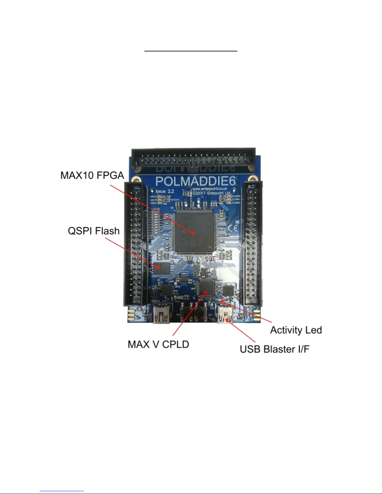
Using the Quartus PRIME programmer the JTAG chain appears like this:
Figure 9– Polmaddie6 JTAG CHAIN
The Max10 FPGA has internal flash memory to hold the configuration data as well as User Flash
Memory UFM which can be accessed and programmed by the FPGA. This UFM can be used to
store user configuration information or additional program storage under the control of a NIOS
CPU.
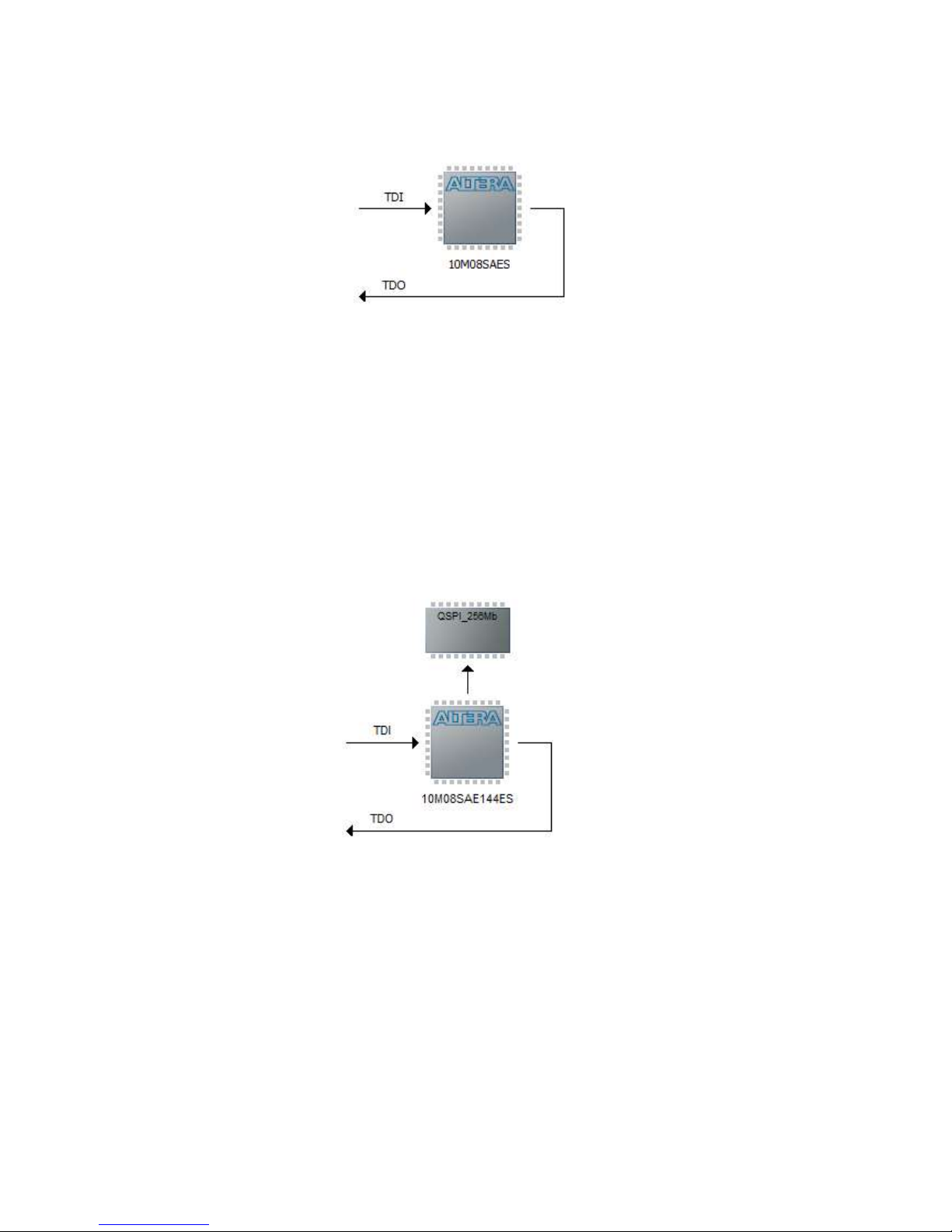
The QSPI 256Mb Flash can be accessed directly from the JTAG Programmer using the Altera
QPFL IP where the QSPI device will appear as follows:
Figure 10– Polmaddie6 QSPI JTAG CHAIN
The QSPI can be used to store larger execute in place (EXIP) programs for use with the NIOS II
processor or can be used as NIOS accessible Flash storage for images and data.
Page 16
© Enterpoint Ltd. – Polmaddie6 Manual – Issue 2.2 05/05/2017
16
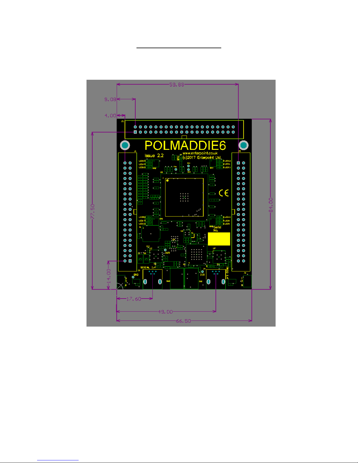
Mechanical Arrangement
Dimensions are in millimetres. The three 40-way connectors are arranged on a 0.1 inch grid relative
to each other.
Figure 11– Polmaddie6 Mechanical Arrangement
The PCB is 1.6mm thick and the tallest components are the3 Boxed Headers which are
approximately 10mm high. Dimensions are subject to manufacturing tolerances.
Page 17

© Enterpoint Ltd. – Polmaddie6 Manual – Issue 2.2 05/05/2017
17
Medical and Safety Critical Use
Polmaddie6 boards are not authorised for the use in, or use in the design of, medical or other safety
critical systems without the express written person of the Board of Enterpoint. If such use is
allowed the said use will be entirely the responsibility of the user. Enterpoint Ltd will accepts no
liability for any failure or defect of the Polmaddie6 board, or its design, when it is used in any
medical or safety critical application
Warranty
Polmaddie6 comes with a 90 return to base warranty. Enterpoint reserves the right not honour a
warranty if the failure is due to maltreatment of the Polmaddie6 board.
Outside the warranty period Enterpoint offers a fixed price repair or replacement service. We
reserve the right not to offer this service where a Polmaddie6 has been maltreated or otherwise
deliberately damaged. Please contact support if need to use this service.
Other specialised warranty programs can be offered to users of multiple Enterpoint products.
Please contact sales on [email protected] if you are interested in these types of warranty,
Support
Enterpoint offers support during normal United Kingdom working hours 9.00am to 5.00pm. Please
examine our Polmaddie6 FAQ web page and the contents of this manual before raising a support
query. We can be contacted as follows:
Page 18

Mouser Electronics
Authorized Distributor
Click to View Pricing, Inventory, Delivery & Lifecycle Information:
Enterpoint:
PM6-10M08-C8
 Loading...