

entegris A192-81M-0215, A192-80M-0215, A192-82M-0215, A198-80M-47C02, A198-80MB-47C02 Installation And Use Manual
...
Datum A
CRITICAL MATERIALS HANDLING
200 MM WAFER CARRIER
INTERFACE MANUAL
Installation and use manual
B3
D1
B2
D3b
BB
D3a

Table of Contents
200 MM WAFER CARRIER INTERFACE
Overview ............................................ 1
General Terminology and Definitions ......... 2
Definitions .............................................3
Wafer Plane ........................................ 4
Specification Purpose ............................... 4
Benefits ................................................4
General Definitions .................................. 4
Specification Description ..........................5
Specification Values .................................5
Use with Automated Equipment ..................5
Four Point Contact ................................ 6
Contact Location ..................................... 6
Benefits of Four Point Contact .................... 6
Equipment Interface ................................6
Wafer Carriers Included and Exceptions ........6
General Interface Information .................. 7
Recommended Contact Points ....................6
Print Based Interface Design .....................6
Benefits of Four Point Contact .................... 6
Interface Points: Wafers Horizontal ........... 7
General Recommendations ........................7
Sample Interface Plate .............................7
Contact Area A ........................................ 8
Contact Area B ........................................8
Contact Area C ........................................8
Interface Points: Wafers Vertical .............. 9
General Recommendations ........................9
Sample Interface Plate .............................9
Contact Area A ........................................ 9
Contact Areas B and C ............................. 10
Interface Points: Robotic Handling ........... 10
General Recommendations ...................... 10
Robotic Handling Features ...................... 10
Endwall Flanges .................................... 10
“H” Bar End Flanges ............................... 11
Endwall Handle ..................................... 11
Top Flanges ......................................... 11
Material Information ............................ 12
Material Properties and
Equipment Interface ........................... 12
Static Protection ................................... 12
Moisture Absorption ............................... 12
Applications ......................................... 12
Wafer Transport Carriers ........................ 12
Process Wafer Carriers ........................... 13
Detailed Material Properties ..................13
For More Information ...........................14
Terms and Conditions ...........................14
Product Warranties .............................. 14
Overview
At Entegris, we are committed to working with you, the equipment
supplier, to provide simple solutions for our joint customers in the
semiconductor industry. Our experience has shown that semiconductor manufacturers want to order their equipment and their wafer carriers without worrying about wafer carrier/equipment interface
issues. By sharing information with you we can provide our joint
customers a compatible equipment and wafer
carrier combination.
ENTEGRIS, INC. INSTALLATION AND USE MANUAL 1
200 MM WAFER CARRIER INTERFACE
D6b
General Terminology and Definitions
This section contains dimensions called out on standard
carrier drawings. These dimensions, as well as general wafer
carrier terms, are defined below.
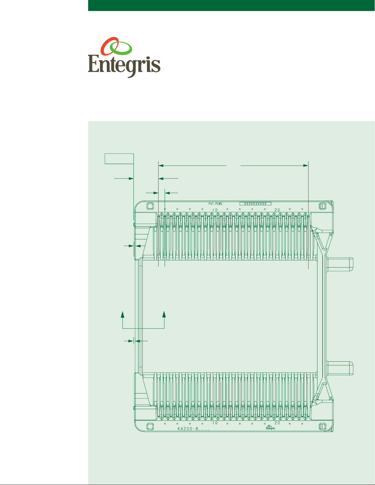
Number Description
OVERALL DIMENSIONS
A1 Length
A2 Width (with/without flanges) includes stripper rails
A3 Height (excluding pin)
CAPACITY
B1 Pockets per carrier
B2 Pocket spacing
B3 Center distance from the first to last pocket
DETAIL DIMENSIONS
C1 Pocket width
C2 Pocket depth
C3 Pocket flat
C4 Pocket size (inside pocket across to
MACHINE FIT SPECIFICATIONS
D1 Distance from Datum A to the center line of the
D3a Distance from Datum A to the front of the
D3b Distance from Datum A to the front of the “H”
D4a Distance from Datum B to the center line of the
D4b Distance from Datum B to the center line of the
D5a Bar web width
D5b Bar width
D5c Distance from Datum A to the front of the
D6a Inside width of the bottom track
D6b Overall width of the “H” bar at the top of the
D8a Overall width of the robotic pick-up flanges
inside pocket)
first pocket
“H” bar at the center of the carrier
bar 13 mm (0.5”) from the side of the carrier
D3b
“H” bar
wafer
D3a
“H” bar web
wafer carrier
D4a
EE
Section A-A
-A-
D1
B2
BB
-A-
A
D6a
D8a
A2
C4
Wafer
D4b
B3
A1
D5c
C11
D5a
D5b
C3
C2
Section E-E
Section B-B
-B-
A
A3
2 INSTALLATION AND USE MANUAL ENTEGRIS, INC.

Definitions
200 MM WAFER CARRIER INTERFACE
Bar end
Crossbar
End wall
Flange
”H“ bar
Hole
Left side
Overall size
Pin
Pocket
Pocket flat
Pocket spacing
Pocket width
Right side
Track clearance
Wafer transfer
See “H” bar.
The mass of material connecting the two sides of the carrier at the bar end
of the carrier.
The wall of the carrier opposite the “H” bar end of the carrier.
Mass of material on the exterior of a carrier, perpendicular to the side walls.
The end of the wafer carrier that has only one crossbar and is capable of
elevator equipment interface.
The area for the pin of another carrier to enter for transferring wafers.
The left side of the carrier when viewed from the “H” bar end while
positioned on its track.
Overall size is measured by length by width by height as shown in the diagram.
Pin height is not included in the height measurement for wafer carriers.
The mass of material which enters the hole or slot of another carrier for
transferring wafers.
The area in which the wafer is located in the carrier.
The width of the pocket along the vertical walls at its most narrow distance.
The distance between pocket centerlines.
The width of the pocket at its widest distance.
The right side of the carrier when viewed from the “H” bar end while
positioned on its track.
The unobstructed area between the two carrier sides on the bar end.
The act of relocating wafers from one carrier into another.
ENTEGRIS, INC. INSTALLATION AND USE MANUAL 3

200 MM WAFER CARRIER INTERFACE
Wafer Plane
This section provides an explanation of the
wafer plane concept and discusses the benefits
of an improved wafer plane. Carriers that hold
each wafer in a predictable location perform
better on automated wafer transfer equipment.
A carrier that does not hold wafers in a predictable
location can cause numerous robotics and wafer
transfer problems. To reduce these problems,
Entegris continually strives to improve wafer
plane dimensions.
Specification Purpose
The wafer plane specification provides the specific,
predictable location of each wafer in a carrier.
Benefits
The benefits of an improved wafer plane include:
• Reduced equipment adjustments
• Improved accuracy in wafer transfers
• Minimized missed wafer transfers
• Reduced equipment shut downs
• Minimized damage or breakage of wafers
• Reduced particle generation caused by wafers
rubbing on carriers
General Definitions
The following definitions define and clarify the
wafer plane concept:
Wafer plane
Wafer plane
zone
Pocket center
plane
Wafer seated
surface
Offset
dimension
Datum A
Datum B
The position of the wafer in a carrier.
The acceptable position for a wafer,
defined by the offset dimension and
tolerance.
The imaginary plane that exactly
bisects each pocket.
The bottom of the wafer, typically the
unfinished side of a wafer in process.
All dimensional data is derived from
this surface.
The distance from the pocket center
plane to the bottom, or seated surface
of the wafer.
The flat surface defined by the “H” bar
end of a wafer carrier. Datum A can be
established by placing the carrier “H”
bar end down on a flat surface.
The flat surface defined by the bottom,
or track of the carrier. Datum B can be
established by placing the carrier track
end down on a flat surface.
4 INSTALLATION AND USE MANUAL ENTEGRIS, INC.
 Loading...