

Page 1

RFID UHF Short Range Controller
RF2400
Product Specification
Revision 1.0
Prepared by: Synergy Technology, Inc. & Synaptec Enterprises, Inc.
Author: Richard L. Hicksted & Michael A. Spahr
________________________________________________________________________
- C
ONFIDENTIAL
3/30/2008
-
Page 2

L
EGAL NOTICES
Copyright © 2007 Ensyc Technologies. All rights reserved.
Ensyc Technologies maintains intellectual property rights pertaining to technology
incorporated in the product(s) described in this document; including without limitation
certain patent rights or patent pending applications in the U.S. and other countries
This document and related product(s) are distributed under licenses restricting use,
copying, distribution, and decompilation. No part of this documentation may be
reproduced without prior written consent of Ensyc Technologies
FCC C
OMPLIANCE
Every effort has been made to design and manufacture this product in accordance with
the limits for a Class A digital device, pursuant to Part 15 of the FCC Rules. These limits
are designed to limit interference when the equipment is used in a commercial
environment. The related equipment generates, uses, and radiates radio frequency energy
and if not installed and used in accordance with this specification may cause harmful
interference with radio communications. Operation in a residential area is likely to result
in interference in which case the user will be required to correct the interference at his
expense.
It is the responsibility on an OEM to obtain certification to operate per FCC Part 15
Subpart A Section 15.21 regulations for the entire system into which this product is
installed.
FCC RF R
ADIATION EXPOSURE STATEMENT
:
The antenna(s) used for this transmitter must be installed to provide a separation distance
of at least 20 cm from all persons and must not be co-located or operating in conjunction
with any other antenna or transmitter. End-users and installers must be provided with
antenna installation instructions and transmitter operating conditions for satisfying RF
exposure compliance.
________________________________________________________________________
- C
ONFIDENTIAL
3/30/2008
-
Page 3

NOTE
Part 15.21
Changes or modifications not expressly approved by the
party responsible for compliance could void the user’s
authority to operate the equipment.
NOTE: The manufacturer is not responsible for any radio
or TV interference caused by unauthorized modifications to
this equipment. Such modifications could void the user’s
authority to operate the equipment.
________________________________________________________________________
- C
ONFIDENTIAL
3/30/2008
-
Page 4

Table of Contents
1 Scope...................................................................................................................................................1
2 Revision History..................................................................................................................................3
3 Reference Documents .........................................................................................................................5
3.1 Specifications & Requirements.........................................................................................5
3.2 Reference Material ............................................................................................................5
4 Overview.............................................................................................................................................7
4.1 DSP Processor...................................................................................................................8
4.2 Transmitter Circuitry.........................................................................................................8
4.3 Receiver Circuitry .............................................................................................................9
4.4 User Interface....................................................................................................................9
4.5 Power Regulation ..............................................................................................................9
4.6 Battery Operation ..............................................................................................................9
5 Functional Description........................................................................................................................11
5.1 Host Protocol.....................................................................................................................11
5.1.1 Message Format...............................................................................................11
5.1.1.1 Message Packet Format.................................................................12
5.1.1.2 Host-to-Reader Payload.................................................................12
5.1.1.3 Reader-to-Host Payload.................................................................13
5.1.1.4 Response Data Formats .................................................................15
5.1.1.4.1 Simple Command Response ........................................15
5.1.1.4.2 Low-Level Command Response..................................15
5.1.1.4.3 Error Response.............................................................15
5.1.2 Reader Commands...........................................................................................16
5.1.2.1 Get Firmware Version (0x00)........................................................16
5.1.2.2 Set Baud Rate (0x03).....................................................................17
5.1.2.3 Set IO Port Value (0x05)...............................................................17
5.1.2.4 Get IO Port Value (0x06) ..............................................................18
5.1.2.5 Get Reader Status (0x0F) ..............................................................18
5.1.2.6 Get Reader Hardware Information (0x11).....................................19
5.1.2.7 Set Reader Hardware Information (0x13) .....................................20
5.1.2.7.1 Paper Sensor Triggered Read ......................................21
5.1.2.8 Set Bi-Directional I/O DDR (0x16)...............................................22
5.1.2.9 Get Bi-Directional I/O DDR (0x17)..............................................22
5.1.3 Tag Commands................................................................................................23
5.1.3.1 Sleep Tag (0x21) ...........................................................................23
5.1.3.2 Get Tag ID (0x24) .........................................................................23
5.1.3.3 Auto Get Tag ID (0x26) ................................................................24
5.1.3.4 Dump ID Data (0x28)....................................................................25
5.1.3.5 Get Raw Tag ID (0x3E).................................................................26
5.1.3.6 Program Tag (0x50).......................................................................27
5.1.3.7 Erase Tag (0x51) ...........................................................................28
5.1.3.8 Kill Tag (0x52)..............................................................................29
5.1.3.9 Lock Tag (0x53)............................................................................30
5.1.3.10 Program Tag Init (0x54)................................................................31
5.1.3.11 LockG2 (0x55) ..............................................................................32
5.1.3.12 Access G2 (0x56) ..........................................................................34
5.1.3.13 Read Tag Memory (0x57) .............................................................35
5.1.3.14 Write Tag Memory (0x58).............................................................36
5.2 Service Port Commands....................................................................................................37
5.2.1 Standard Commands........................................................................................37
5.2.1.1 Baud Rate (baud) command..........................................................37
________________________________________________________________________
P
i
RODUCT SPECIFICATION
Page 5

5.2.1.2 Transmit Power Step (Txp[0-3]) command...................................37
5.2.1.3 Receive Threshold (rxt) command ................................................38
5.2.1.4 Phase (phs) command....................................................................38
5.2.1.5 Tag Class (tc) command................................................................39
5.2.1.6 Read Retry (rrty) command...........................................................39
5.2.1.7 Read Tag (rt) command.................................................................39
5.2.1.8 Read Loop (rl) command...............................................................39
5.2.1.9 Sequential Loop (sl) command......................................................40
5.2.1.10 Write Tag (wt) command...............................................................40
5.2.1.11 Lock Tag (lt) command .................................................................40
5.2.1.12 Lock Tag G2 (l2) command...........................................................41
5.2.1.13 Access (apw)..................................................................................41
5.2.1.14 Kill Tag (kt) command...................................................................41
5.2.1.15 Quiet Tag (qt) command................................................................41
5.2.1.16 Erase Tag (et) command................................................................42
5.2.1.17 Paper Sensor Triggered Read (pstr) command..............................42
5.2.1.18 Paper Sensor (ps) command ..........................................................42
5.2.1.19 Paper Sensor Threshold (pst) command ........................................43
5.2.1.20 Auto Read Tag (art) command......................................................43
5.2.1.21 Dump ID Data (did) command......................................................44
5.2.1.22 Program Flash (pf) command ........................................................44
5.2.1.23 Speaker Test (st) command............................................................44
5.2.1.24 Beep (beep) command...................................................................45
5.2.1.25 Set EEPROM Defaults (eedef) command......................................45
5.2.1.26 Read EEPROM (ree) command.....................................................45
5.2.1.27 No initial message (noim) command .............................................45
5.2.1.28 Diagnostic (di) command ..............................................................46
5.2.1.29 Ignore CRC (icrc) command .........................................................48
5.2.1.30 Exit (exit) command.......................................................................48
5.2.1.31 Display menu (??) command.........................................................48
5.2.1.32 Standard command summary.........................................................49
5.2.2 Protected Commands.......................................................................................50
5.2.2.1 Password (pw) command...............................................................50
5.2.2.2 Transmit power (txp) command.....................................................50
5.2.2.3 Maximum transmit power (txpmax) command..............................50
5.2.2.4 Minimum transmit power (txpmin) command...............................50
5.2.2.5 Channel select (chan) command....................................................51
5.2.2.6 Hop (hop) command......................................................................52
5.2.2.7 Gen2 Read (g2r) command ...........................................................52
5.2.2.8 Gen2 Write (g2w) command .........................................................52
5.2.2.9 Transmit zeros (t0) command........................................................52
5.2.2.10 Transmit ones (t1) command.........................................................53
5.2.2.11 Transmit alternating (ta) command ...............................................53
5.2.2.12 Transmit random (tr) command.....................................................53
5.2.2.13 Transmit data (td) command..........................................................53
5.2.2.14 Carrier on (con) command.............................................................54
5.2.2.15 Carrier off (coff) command............................................................54
5.2.2.16 Localization (local) command.......................................................54
5.2.2.17 Chipcon register read (ccr) command............................................54
5.2.2.18 Chipcon register write (ccw) command.........................................54
5.2.2.19 Protected command summary........................................................55
5.2.3 Service port error codes...................................................................................56
5.3 Radio Frequency Interface ................................................................................................57
________________________________________________________________________
P
ii
RODUCT SPECIFICATION
Page 6

5.3.1 Auto-ID Class 1...............................................................................................57
5.3.1.1 Class 1 Reader-Tag RF communications.......................................57
5.3.1.2 Class 1 Tag-Reader RF communications.......................................58
5.3.2 Class 1 – Gen 2................................................................................................59
5.3.2.1 Gen 2 Reader-Tag RF communications.........................................59
5.3.2.2 Gen 2 Tag-Reader RF communications.........................................60
5.4 Logical Structures and Data content..................................................................................62
5.4.1 Gen 2 Tag Structures and Data content...........................................................62
5.5 Autonomous Operation .....................................................................................................63
6 Hardware Description .........................................................................................................................65
6.1 Host Communication Interface..........................................................................................66
6.2 DSP Processor...................................................................................................................67
6.3 EEPROM...........................................................................................................................67
6.4 Transmitter/VCO...............................................................................................................68
6.5 Power Splitter....................................................................................................................68
6.6 Power Amplifier................................................................................................................68
6.7 PA Modulation..................................................................................................................68
6.8 Directional Coupler/RF FIlter ...........................................................................................69
6.9 Selectable LC Phase Delay/Mixer.....................................................................................69
6.10 Base-band Amplifier .........................................................................................................69
6.11 General Purpose Digital I/O Port ......................................................................................70
6.12 Digital I/O Interface ..........................................................................................................71
6.13 Buzzer Circuit....................................................................................................................72
6.14 Optical Sensor Interface....................................................................................................72
6.15 Power Regulators ..............................................................................................................73
7 Specifications......................................................................................................................................75
7.1 Electrical Specifications....................................................................................................75
7.1.1 RF Interface.....................................................................................................75
7.1.2 Communications Interface...............................................................................75
7.1.3 Power Supply ..................................................................................................75
7.1.4 Battery (optional).............................................................................................76
7.2 Environmental Specifications............................................................................................76
7.3 Mechanical Specifications.................................................................................................76
7.4 I/O Connectors ..................................................................................................................77
________________________________________________________________________
P
iii
RODUCT SPECIFICATION
Page 7

Figures
Figure 4-1
Figure 5-1
Figure 5-2
Figure 5-3
Figure 5-4
Figure 5-5
Figure 5-6
Figure 5-7
Figure 5-8
Figure 5-9
Figure 6-1
Figure 6-2
Figure 6-3
Figure 6-4
Figure 6-5
Figure 6-6
Figure 6-7
Figure 7-1
RF2400 Block Diagram __________________________________________________ 7
Message Packet Format _________________________________________________ 12
Host to Reader Payload Format___________________________________________ 12
Reader to Host Payload Format___________________________________________ 13
Low-Level Command Response ___________________________________________ 15
Class 1 Reader Modulation Timing for Binary 0______________________________ 58
Class 1 Reader Modulation Timing for Binary 1 ______________________________ 58
Class 1 Tag to Reader Encoding __________________________________________ 59
Gen 2 Reader to Tag PIE Encoding ________________________________________ 60
Gen2 Tag to Reader Encoding ____________________________________________ 61
Host Interface _________________________________________________________ 66
Digital I/O Port________________________________________________________ 70
Digital I/O Interface ____________________________________________________ 71
Buzzer Circuit_________________________________________________________ 72
Optical Sensor Interface_________________________________________________ 72
Main Power 4.2V Regulator ______________________________________________ 73
+3.3V and +1.8V Regulator ______________________________________________ 73
RF2400 Mechanical Assembly ____________________________________________ 78
________________________________________________________________________
P
iv
RODUCT SPECIFICATION
Page 8

Tables
Table 5-1
Table 5-2
Table 5-3
Table 5-4
Table 5-5
Table 5-6
Table 5-7
Table 5-8
Table 5-9
Table 5-10
Table 5-11
Table 5-12
Table 5-13
Table 5-14
Table 5-15
Table 5-16
Table 5-17
Table 5-18
Table 5-19
Table 5-20
Table 5-21
Table 5-22
Table 5-23
Table 5-24
Table 5-25
Table 5-26
Table 5-27
Table 5-28
Table 5-29
Table 5-30
Table 5-31
Table 5-32
Table 5-33
Table 5-34
Table 5-35
Table 5-36
Table 5-37
Table 5-38
Table 5-39
Table 5-40
Table 5-41
Table 5-42
Message Encapsulation Characters ________________________________________ 12
Command/Response Payload Fields _______________________________________ 13
Communication Codes __________________________________________________ 14
Low-Level Response Fields ______________________________________________ 15
Get Firmware Version __________________________________________________ 16
Set Baud Rate _________________________________________________________ 17
Set IO Port Value ______________________________________________________ 17
Get IO Port Value______________________________________________________ 18
Get Reader Status ______________________________________________________ 18
Get Reader Hardware Information_________________________________________ 19
Set Reader Hardware Information _________________________________________ 20
Set Bi-Directional I/O DDR ______________________________________________ 22
Get Bi-Directional I/O DDR______________________________________________ 22
Sleep Tag ____________________________________________________________ 23
Get Tag ID ___________________________________________________________ 23
Auto Get Tag ID _______________________________________________________ 24
Dump ID Data Command________________________________________________ 25
Get Raw Tag ID _______________________________________________________ 26
Program Tag__________________________________________________________ 27
Erase Tag ____________________________________________________________ 28
Kill Tag______________________________________________________________ 29
Lock Tag _____________________________________________________________ 30
Program Tag Init ______________________________________________________ 31
LockG2 ______________________________________________________________ 32
Lock bit usage_________________________________________________________ 33
Lock action field functionality ____________________________________________ 33
AccessG2_____________________________________________________________ 34
Read Tag Memory______________________________________________________ 35
Write Tag Memory _____________________________________________________ 36
Service Port Lead-in sequence ____________________________________________ 37
Transmit Power Level___________________________________________________ 38
Service Port Commands - Standard ________________________________________ 49
RF2400 USA Hopping Table _____________________________________________ 51
RF2400 E.U. Hopping Table TBD _________________________________________ 51
RF2400 Japan Hopping Table TBD________________________________________ 51
Service Port Commands - Protected________________________________________ 55
Service Port Error Codes ________________________________________________ 56
Class 1 Reader-Tag Modulation Parameters_________________________________ 57
Class 1 Tag-Reader Communication Parameters _____________________________ 58
Gen 2 Reader-Tag Modulation Parameters __________________________________ 60
Gen 2Tag-Reader Communication Parameters _______________________________ 61
Class 1 Gen 2 Memory Map ______________________________________________ 62
________________________________________________________________________
P
v
RODUCT SPECIFICATION
Page 9

________________________________________________________________________
P
vi
RODUCT SPECIFICATION
Page 10

RFID UHF Short Range Controller (RF2400)
__________________________________________________________________________
1 SCOPE
This document is a detailed technical specification for the RFID UHF Short Range
Controller (RF2400). It provides a comprehensive description of the hardware with
detailed design notes and a complete functional description of the product. This
document is contains proprietary and confidential information and is not intended to be
used as an end user’s manual.
________________________________________________________________________
Ensyc
- C
Technologies P
ONFIDENTIAL
AGE
1 11:56:13 AM
- M
ARCH
30, 2008
Page 11

Page 12

RFID UHF Short Range Controller (RF2400)
__________________________________________________________________________
2 REVISION HISTORY
1.0 11/28/07 Initial Release
________________________________________________________________________
Ensyc
- C
Technologies P
ONFIDENTIAL
AGE
3 11:56:13 AM
- M
ARCH
30, 2008
Page 13

Page 14

RFID UHF Short Range Controller (RF2400)
__________________________________________________________________________
3 REFERENCE DOCUMENTS
The following documents form part of this specification to the extent specified herein. In
the event of a conflict between the requirements of this specification and the associated
product drawings, referenced documents or firmware listings, the drawings, documents
and listings shall take precedence.
3.1 SPECIFICATIONS & REQUIREMENTS
MIT Auto-ID Center – Operational Specification for a UHF Radio Frequency Identification (RFID) System – Part I.
Class 1 UHF Devices - May 29, 2002
MIT Auto-ID Center – Technical Report - 860MHz–930MHz Class 1 Radio Frequency Identification Tag Radio
Frequency & Logical Communication Interface Specification Candidate Recommendation, Version 1.0.1 – November
14, 2002
EPC™ Radio-Frequency Identity Protocols Class-1 Generation-2 UHF RFID Protocol for Communications at 860
MHz – 960 MHz Version 1.0.9 – January 31, 2005
FCC - Title 47 Part 15.247 – Operation within the bands 902-928MHz, 2400-2483.5 MHz, and 5725-5850 MHz.
3.2 REFERENCE MATERIAL
Texas Instrument – TMS320F2808 Data Manual – SPRS230H – October 2003-Revised June 2006
Chipcon AS / Texas Instrument – CC1070 Single Chip Low Power RF Transmitter for Narrowband Systems –
SWRS043 - Rev 1.3
Chipcon AS – AN014 Frequency Hopping Systems (Rev 1.0) – 2002-03-20
Hittite Microwave Corporation – HMC545 GaAs MMIC SPDT Switch, DC-3 GHz – V00.0905
Triquint Semiconductor – TQM7M4006 - 3V Quad-Band GSM850/GSM900/DCS/PCS Power Amplifier Module Data
Sheet-Revision E – February 22, 2006
Mini-Circuits – ADE-2 – Surface Mount Frequency Mixer Level 7 (LO Power +7dBm) 5 to 1000MHz REV. D. –
M102713, RVN/TD/CP/AM 070412
Linear Technology – LT6231 – 215MHz, Rail-to-Rail Output, 1.1nV/Hz
623012fs
Analog Devices – ADG723 – CMOS, Low Voltage, 4Ω Dual SPST Switch – Rev B - C00045-0-2/07(B)
Analog Devices – ADG823 - <1 Ω 1.8V to 5.5V, Dual SPST Switch – REV.0 – C02851-0-8/02(0)
1/2
, 3.5mA Op Amp Family – sn623012
________________________________________________________________________
Ensyc
- C
Technologies P
ONFIDENTIAL
AGE
5 11:56:13 AM
- M
ARCH
30, 2008
Page 15

Page 16
RFID UHF Short Range Controller (RF2400)
__________________________________________________________________________
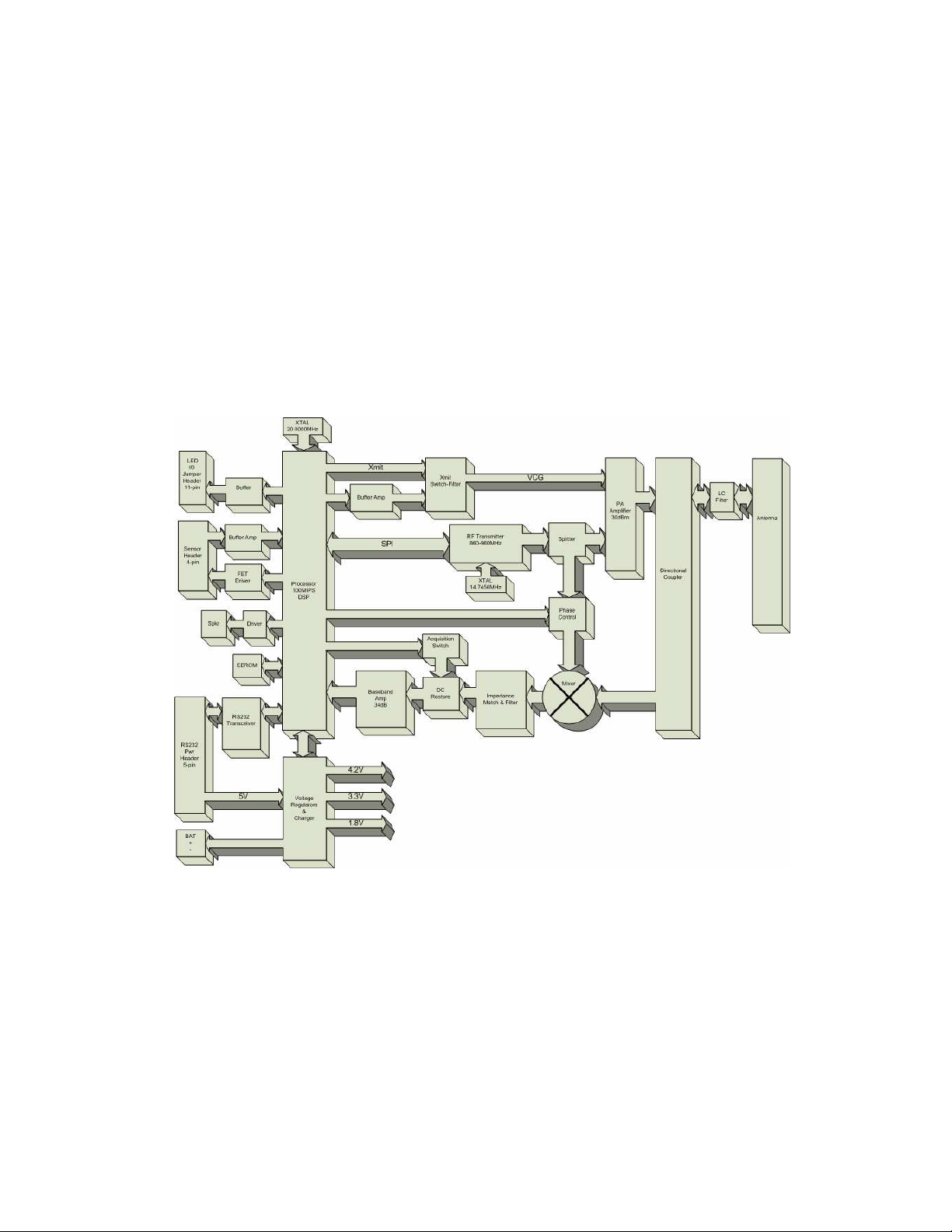
4 OVERVIEW
The RF2400 RFID Controller is a low cost implementation of a UHF RFID reader
designed specifically for short range applications. The Controller has been designed to
read, write, and verify EPC Class 1 and Generation 2 tags, is implemented as a single
electronics module and requires a separate antenna. (Refer to Figure 4-1)
Figure 4-1 RF2400 Block Diagram
________________________________________________________________________
Ensyc
- C
Technologies P
ONFIDENTIAL
AGE
7 11:56:13 AM
- M
ARCH
30, 2008
Page 17

RFID UHF Short Range Controller (RF2400)
__________________________________________________________________________
4.1 DSP PROCESSOR
The heart of the RF controller is a 100 MIPS DSP processor. The processor
communicates with the host over an RS232 interface using a media independent protocol.
Message packets from the host direct all RF2400 reader operations and upon completion
the processor sends a response packet.
The processor is interfaced to a highly integrated single chip UHF transmitter/VCO over
an SPI bus which provides the RF carrier and Frequency Hopping Spread Spectrum
(FHSS) signaling. Using a PWM the processor establishes the gain of a RF amplifier and
amplitude shift keys (ASK) modulates the carrier by switching this signal on/off.
The processor demodulates the backscatter signal from a tag using a high-pass filter and a
FET switch to remove the DC component from the signal and samples the output of the
base-band amplifier using a 12-bit A/D input. The processor phase locks to the signal,
synchronizes to clock edges, and follows the average signal level/gain to properly decode
the data.
Additionally, the processor controls an optical sensor to identify the presence of a tag to
implement auto interrogation. A scheme involving modulation of the sensor emitter and
demodulation of the reflected signal is used as a means to suppress ambient light and
improve the reliability of the sensor. The sensor input can be configured as a switch
input and used to manually trigger reads.
Finally, the processor drives several LEDs to indicate power, activity and error
conditions as well as a speaker to attract user attention.
4.2 TRANSMITTER CIRCUITRY
An integrated single chip transmitter is used and controlled by the DSP processor to
produce the RF carrier required to communicate with a UHF RFID tag. Additionally,
this component incorporates the necessary circuitry to implement Frequency Hopping
Spread Spectrum (FHSS) signaling for noisy environments and to meet agency spectral
requirements. To enhance speed of operation, the Transmitter/VCO includes dual sets of
frequency control registers to allow overlapped frequency configuration during operation.
UHF frequency is synthesized from an inexpensive crystal using a programmable
fractional divider to achieve high resolution and is ideal for narrow band applications. An
external loop filter is provided to meet the stabilization requirements imposed by FHSS.
A power splitter is used to divide the VCO output for use as both a local oscillator and
RF carrier. An LC phase shifter between the splitter and mixer is used to select the inphase and 90 degree phase components providing a mechanism to compensate for the
phase of the received signal
A 2-watt GSM Power Amplifier is used to boost the RF carrier and is adjustable from
0dBm (1mW) to 24dBm (250mW). The amplifier is designed for low cost cellular phone
applications and requires only a few external power filtering components. Output power
is adjusted using a voltage control input from the DSP processor. A PWM output sets the
voltage which is filtered by a 2-pole Sallen-Key low-pass filter. The filtered voltage is
________________________________________________________________________
Ensyc
- C
Technologies P
ONFIDENTIAL
AGE
8 11:56:13 AM
- M
ARCH
30, 2008
Page 18

RFID UHF Short Range Controller (RF2400)
__________________________________________________________________________
switched to the power amplifier through two independent time constants. This shaping
meets EPCTM and FCC requirements reducing transmit spurs by controlling the on and
off rate of the power amplifier. The output of the amplifier is connected to the antenna
using a PCB implemented directional coupler with 8dB coupling loss and directivity
between 25dB and 30dB. A LC PI filter couples the output of the filter to the antenna
filtering any harmonic components.
4.3 RECEIVER CIRCUITRY
Tag backscatter is coupled to a precision mixer from the directional coupler. The output
of the mixer is coupled to the receiver circuitry using an impedance matching amplifier.
An acquisition switched high-pass filter removes the DC component before applying the
signal to the 34dB base-band amplifier/800KHz filter. The amplified signal is sampled
by the DSP using a 12-bit A/D input. The DSP processor tracks the average value of the
signal; phase locks to the signal, and synchronizes to the clock edges in order to decode
the data.
4.4 USER INTERFACE
The RF2400 reader is interfaced to the host using an RS232 serial connection.
Commands and responses are communicated using packets. The protocol includes
commands to configure and status the reader as well as commands to program and read
tags. Several LED outputs and an integrated speaker provide user feedback of power,
activity and error conditions. A separate optical sensor interface allows to processor to
sense presence of a tag providing a means to auto interrogate the tag
4.5 POWER REGULATION
The RF2400 reader is powered from a single 5volt power source and requires only 900
mA to provide 24dBm(250mW) of RF power. Main 5 volt power is converted to 4.2
volts by a Li-Ion battery charger. This can charge an optional battery for portable
operations. The 4.2V power is used directly by the RF power amplifier but also feeds the
3.3volt low noise RF power and 1.8 volt processor core voltage LDO regulators.
4.6 BATTERY OPERATION
An optional 3.7V 3200mA/hr Li-Ion battery can be used for remote operation. A battery
charging circuit maintains the battery voltage between 4.0 and 4.1V. In order to extend
battery life and prevent overheating and the possibility of explosion, both the battery and
charging circuit include protection circuitry. Additionally, firmware monitors the charge
state and shuts down the charger when the battery is fully charged.
While operating on battery, steps have been taken to reduce the operating current in order
to extend the operational time between charges. Normally the processor runs at
100MHz, which is required while accessing tags. When idle, the processor clock is
decreased to 20 MHz, greatly reducing the required current.
________________________________________________________________________
Ensyc
- C
Technologies P
ONFIDENTIAL
AGE
9 11:56:13 AM
- M
ARCH
30, 2008
Page 19

Page 20

RFID UHF Short Range Controller (RF2400)
__________________________________________________________________________
5 FUNCTIONAL DESCRIPTION
The RF2400 reader is a radio frequency identification (RFID) communication interface
designed specifically for short range applications. The reader interfaces to a host
processor with an industry standard RS232 or optional USB interface adapter using a
media independent protocol. The RF2400 reader supports the reader commanded
functionality required for both the Auto-ID Center Class1 and Gen 2 Tags operating in
the frequency range of 860MHz-960MHz.
5.1 HOST PROTOCOL
This section describes the format and commands for the bi-directional communication
between the RF2400 reader and the host including command codes, parameters, and
response data.
Commands are divided into several code groups:
00 – 1F setting and retrieving RF2400 reader parameters
20 – 3F reader-to-tag modulation commands that return a single response message
40 – 4F reader-to-tag modulation commands that result in a tag-list response
50 – 5F tag programming commands
60…6F setting and retrieving RF2400 reader configuration data
D0 – DF loading RF2400 firmware code
F0 – FF reserved for managing a tag list
The following section describes the binary protocol for serial communication between
the host and the RF2400 Module. This protocol is media independent and can be
implemented using RS232, USB, or other serial interfaces
5.1.1 Message Format
Messages encapsulate commands from the host and responses from the RF2400 reader
that are sent as packets over the serial interface between the host and the RF2400 reader.
________________________________________________________________________
Ensyc
- C
Technologies P
ONFIDENTIAL
AGE
11 11:56:13 AM
- M
ARCH
30, 2008
Page 21
RFID UHF Short Range Controller (RF2400)
__________________________________________________________________________
5.1.1.1 Message Packet Format
Messages between the host and reader are binary data packets, consisting of a message
payload encapsulated with two bytes preceding any message (
completing any message (
[DLE][EOM]
). All communications are initiated by the host.
[DLE][SOM]
) and two bytes
(Refer to Figure 5-1 and Table 5-1)
Note: ITEMS IN PARENTHESIS (…) ARE NOT REQUIRED FOR ALL MESSAGES.
[DLE] [SOM] [Payload] [DLE] [EOM]
Figure 5-1 Message Packet Format
Token Description
[DLE]
[SOM]
[EOM]
Data Link Escape token; 0x10
Start of Message token; 0x01
End of Message token; 0x02
Table 5-1 Message Encapsulation Characters
In order to avoid ambiguities, if a data value in the payload is a DLE (0x10) character, the DLE (0x10) is
repeated as the message packet is formed.
5.1.1.2 Host-to-Reader Payload
The host to reader payload includes a session identification
number
(CommandData)
[Reader#]
,
a command to execute
, followed by a two byte CRC
[Command]
[CRC-CCITT16]
[SessionID]
,
optional command data
,
a target reader
. (Refer to Figure 5-2 and
Table 5-2)
[SessionID] [Reader#] [Command] (CommandData) [CRC-CCITT-16]
Figure 5-2 Host to Reader Payload Format
________________________________________________________________________
Ensyc
- C
Technologies P
ONFIDENTIAL
AGE
12 11:56:13 AM
- M
ARCH
30, 2008
Page 22
RFID UHF Short Range Controller (RF2400)
__________________________________________________________________________
5.1.1.3 Reader-to-Host Payload
The reader to host payload includes a session identification
number
[CommCode],
CCITT16]
[Reader#]
,
the command executed
optional response data
[CommandEcho],
(ResponseData)
, followed by a two byte CRC
. (Refer to Figure 5-3, Table 5-2 and Table 5-3)
[SessionID]
,
a target reader
type of communication
[SessionID] [Reader#] [CommandEcho] [CommCode] (ResponseData) [CRC-CCITT16]
Figure 5-3 Reader to Host Payload Format
Payload
Field
Description
[CRC-
[SessionID]
[Reader # ]
[Command]
[CommandEcho]
(CommandData)
[CommCode]
(ResponseData)
[CRC-CCITT16]
Single-byte value. Every command gets a new number defined by the host.
Every response matches the session ID of the initiating command. Normal
session IDs can range from 0x01 to 0xFF. A SessionID of 0x00 in a
command message forces the reader to repeat the previous response. This
feature allows the Host to request the previous response in case of a
communication error.
Single-byte value. In a Host command, a Reader # of 0x00 indicates that the
command is addressed to all readers. A Reader will reply to commands only
if its internal RDRNUM matches or if a command is addressed to all readers
The factory default reader number is 0xFF.
Single-byte value. Defines the command to be executed or has been
executed (refer to section 5.1.2 for details).
Variable length value specifying command parameters (refer to the section
5.1.2 for details)
Single-byte value. Indicates the type of message or error. CommType < 0x80
indicates that a valid command was received. CommType >= 0x80 indicates
that an error occurred, either in the command format, parameters, or in the
execution of the command. (refer to Table 5-3 for details)
Contains a variable number of bytes (including none) (refer to section 5.1.1.4
for details).
Two bytes of CRC-CCITT16 polynomial (X^16+X^12+X^5+1) seed 0xFFFF.
The CRC is calculated over all data from Session ID to Response Data
inclusive. DLE packetization is not included into the CRC. The CRC is sent
MSB first, LSB last.
Table 5-2 Command/Response Payload Fields
________________________________________________________________________
Ensyc
- C
Technologies P
ONFIDENTIAL
AGE
13 11:56:13 AM
- M
ARCH
30, 2008
Page 23

RFID UHF Short Range Controller (RF2400)
__________________________________________________________________________
CommCode Description
0x00
0x01
0x02
0x03
0x04
0x05
0x06
0x07
0x08
0x09
0x0A
0x0B
0x0C
0x0D
0x40
0x41
0x81
0x82
0x83
0x84
0x85
0x86
0x87
0x88
0x89
0x8A
0x8B
0x8C
0x8D
0x8E
0x8F
0x90
0x91
0x92
0x93
0x94
0x95
0x96
0x97
0x98
MSGOK Success
STARTINV Starting inventory message
TAGINV Tag Data inventory message
ENDINV Ending inventory message
STARTLIST Starting list dump
RECLIST List dump data record
ENDLIST End of list dump
STARTDIAG Starting diagnostic message
DIAGDATA Diagnostic data message
ENDDIAG End of diagnostic message
UPLOADOK Upload line success
UPLOADEND Upload complete
SUSPEND Reader entering suspend state
RESUME Reader resuming from suspend state
NO PASSW Kill password is locked, can’t be read
LOCKNPW EPC locked but Kill password not set because locked
UNKLEN Unknown message length
UNKVAL Unknown value
UNKCMD Unknown command
UNKTAGCMD Unknown or disabled tag command
OVRERR Overflow error on directed list entry
NOTAG No tag to read or program
ERASEFAIL Erase failure
PROGFAIL Program data verification error
TAGLOCK Tag is locked, cannot program error
KILLFAIL Kill failure
LOCKFAIL Lock attempt failure
DATASIZE Tag data memory size mismatch
HWERR Hardware error
LISTFULL List for directed inventory is full
UPLOADERR Upload line contained an error
UPLOADINV Command invalid for bootloader
UPLOADCRC Upload Program Memory CRC Error
NVFAIL EEPROM error
RESV Reserved
RESV Reserved
UNKIDLEN Unknown ID Length
TAGLOST Tag lost after earlier communication
TAGNXM Addressed word doesn’t exist
LOGFULL EEPROM ID storage is full
Table 5-3 Communication Codes
CommCode < 0x80 indicates a successful operation, CommCode >= 0x80 indicates an error condition of
some kind.
________________________________________________________________________
Ensyc
- C
Technologies P
ONFIDENTIAL
AGE
14 11:56:13 AM
- M
ARCH
30, 2008
Page 24
RFID UHF Short Range Controller (RF2400)
__________________________________________________________________________
5.1.1.4 Response Data Formats
The following sub-sections detail specific response data formats
5.1.1.4.1 Simple Command Response
The RF2400 reader responds to a simple command (for example getting a reader
parameter) with the specified number of bytes.
5.1.1.4.2 Low-Level Command Response
In response to a tag-related low-level command such as Get Tag ID. The Response Data
is sent to the Host in the following format (Refer to Figure 5-4 and Table 5-4)
[TagDecodeStatus] [Antenna#] (TagDataLength) (TagData)
Figure 5-4 Low-Level Command Response
Low-Level
Field
[TagDecodeStatus]
[Antenna # ]
(TagDataLength)
(TagData)
Description
Single-byte value indicating status of data acquisition by a low-level command
0x00 – Good ID
0x01 – No tag
0x02 – Collision
0x03 – CRC Error (returned for Get Tag ID only)
Bit4 – Kill password is locked
Bit5 – Access password is locked
Single-byte value indicating the Antenna number used for the current air
interface transaction. The only valid value for the RF2400 is 0x00
Length of Tag Data in bytes
Included for TagDecodeStatus of 0x00 "GoodID and 0x03 "CRC Error" only
Variable length defined by TagDataLength. Data is sent MSB first ending with
the LSB of the last byte.
Included for TagDecodeStatus of 0x00 "GoodID and 0x03 "CRC Error" only
Table 5-4 Low-Level Response Fields
5.1.1.4.3 Error Response
The RF2400 reader responds to every host command except when a communication error
is detected. If a reader detects a CRC Error in a host payload, the message will be
ignored. However, if the host detects a CRC Error, it may request the previous response
by sending a packet with a
[SessionID]
of zero.
If the host payload is less than four bytes long including the two bytes of CRC (no
Reader# or Command) the reader will ignore the message. If the payload is four bytes
________________________________________________________________________
Ensyc
- C
Technologies P
ONFIDENTIAL
AGE
15 11:56:13 AM
- M
ARCH
30, 2008
Page 25
RFID UHF Short Range Controller (RF2400)
__________________________________________________________________________
long including the two bytes of CRC (no Command), the reader will respond with a 0x81
UNKLEN “unknown message length”
[CommCode]
.
5.1.2 Reader Commands
The RF2400 controller responds to numerous commands using the media independent
format described in paragraph 5.1. These commands provide a mechanism to configure
(Set) the reader as well as retrieve (Get) reader status. The reader will respond to all Set
commands with an echo of
followed by a two byte CRC
will respond to all Get commands with an echo of
[CommCode]
CCITT16]
and a variable length
as described in paragraphs 5.1.1.3 and 5.1.1.4.
[SessionID], [Reader#], [CommandEcho]
[CRC-CCITT16]
(ResponseData)
as described in paragraph 5.1.1.3. The reader
[SessionID], [Reader#], [CommandEcho],
field followed by a two byte CRC
, and
[CommCode]
[CRC-
Any command may result in a
[CommCode]
of one of the following: MSGOK, UNKLEN,
UNKVAL, and UNKCMD as defined in Table 5-1. Other possible codes are identified in
the description of the specific command. If the RF2400 has been initialized into its
integral bootloader firmware, there will be no response to host reader commands
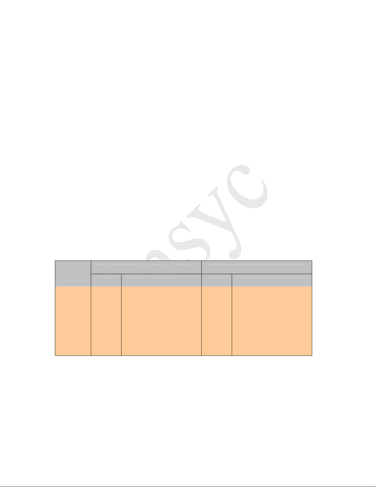
5.1.2.1 Get Firmware Version (0x00)
The Reader will reply with five (5) bytes specifying Localization Code, Reader Type,
and Firmware Version Number. Response data is in binary hex format.
The localization code and the reader type are stored in non-volatile memory and
automatically configured for USA (0x01) operation on the initial firmware upload.
Subsequent firmware updates preserve the existing configuration in non-volatile memory.
Command
Code
0x00 0 Bytes
Size Valid Values Size Valid Values
Command Data Response Date
--
5 Byte
1st Byte -- Localization Code
0x01 -- USA
0x02 -- Japan
0x03 -- E.U.
2nd Byte -- Reader Type
0x09 – RF1200 Reader
0x0A – RF2400 Reader
3rd Byte -- 0x00
4th Byte -- Major Revision #
5th Byte -- Minor Revision #
Table 5-5 Get Firmware Version
COMMAND DLE SOM SesID Rdr# Cmd CRCH CRCL DLE EOM
10 01 01 FF 00 54 0C 10 02
RESPONSE DLE SOM SesID Rdr# Echo Mtype Local Rtype Nused FverH FverL CRCH CRCL DLE EOM
10 01 01 FF 00 00 01 09 00 00 0A 75 A8 10 02
Get Firmware Version Example
Note: this example reflects firmware version V0.10
________________________________________________________________________
Ensyc
- C
Technologies P
ONFIDENTIAL
AGE
16 11:56:13 AM
- M
ARCH
30, 2008
Page 26
RFID UHF Short Range Controller (RF2400)
__________________________________________________________________________
5.1.2.2 Set Baud Rate (0x03)
This command will only accept 0 thru 5 as valid data fields. The reader will respond to
the command at the old baud rate before changing to the new rate. The updated baud rate
will be stored in non-volatile memory replacing the previous value. The factory default
setting is 19,200 baud using 8 data bits, no parity, and one stop bit.
If the user inadvertently sets the baud rate to one not supported by the host, a hardware
reset is provided. Disconnect power from the board, connect pins 1 to 2 of the 11 pin
connector, re-connect power. The EEPROM will be reset to defaults (19,200 baud).
Command
Code
0x03 1 Bytes Baud Rate
Size Valid Values Size Valid Values
Command Data Response Date
0 Byte - 0x00 9,600
0x01 19,200 (default)
0x02 38,400
0x03 57,600
0x04 115,200
Table 5-6 Set Baud Rate
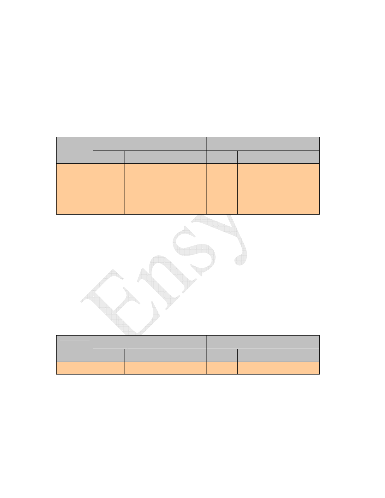
5.1.2.3 Set IO Port Value (0x05)
Sets or clears specified output port pins. Ports start at LSB corresponding to physical port
0 and are bitmapped toward the MSB. The RF 2400 has two bi- directional IO ports. Bits
in the send data with no corresponding physical port will be ignored. Additionally, since
the RF2400 IO ports are bi-directional, the value will be ignored in the case of the
corresponding port pin defined as input. A bit value of 1 in the send data will cause the
corresponding port to be driven high. A bit value of 0 will cause the corresponding port
pin to be pulled low. A Get Reader Hardware Information command can be issued to
determine the number and type of output ports available. The Set Bi-Directional I/O
DDR and Get Bi-Directional I/O DDR commands may be used to setup and determine
the I/O port configuration.
Command
Code
0x05 1 Bytes 0x00 -- 0xFF 0 Byte --
Size Valid Values Size Valid Values
Command Data Response Date
Table 5-7 Set IO Port Value
COMMAND DLE SOM SesID Rdr# Cmd Data CRCH CRCL DLE EOM
10 01 01 FF 05 01 F8 26 10 02
RESPONSE DLE SOM SesID Rdr# Echo Mtype CRCH CRCL DLE EOM
10 01 01 FF 05 00 E8 07 10 02
Set IO Port Value Example
________________________________________________________________________
Ensyc
- C
Technologies P
ONFIDENTIAL
AGE
17 11:56:13 AM
- M
ARCH
30, 2008
Page 27
RFID UHF Short Range Controller (RF2400)
__________________________________________________________________________
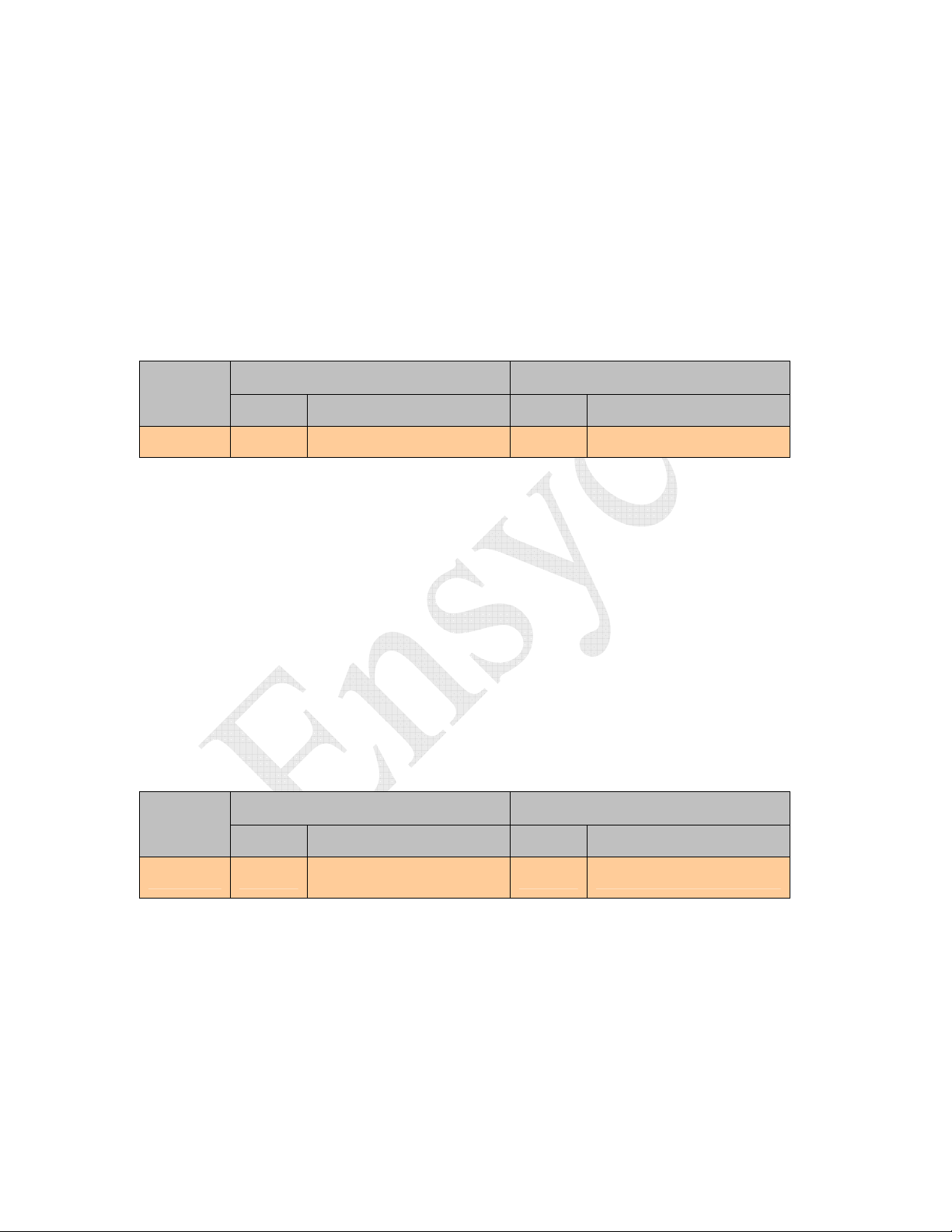
5.1.2.4 Get IO Port Value (0x06)
This command returns the current state of the input port pins. Response data is a bitmap
with the LSB corresponding to physical port 0. The RF2400 reader has two bidirectional ports and will return a 0 bit value for all remaining bit positions.
Additionally, since the RF2400 IO ports are bi-directional, any port defined as an output
will return the current level of the IO port. A Get Reader Hardware Information
command can be issued to request the hardware configuration. The Set Bi-Directional
I/O DDR and Get Bi-Directional I/O DDR commands may be used to setup and
determine the I/O port configuration.
Command
Code
0x06 0 Bytes -- 1 Byte 0x00 -- 0xFF
Size Valid Values Size Valid Values
Command Data Response Date
Table 5-8 Get IO Port Value
COMMAND DLE SOM SesID Rdr# Cmd CRCH CRCL DLE EOM
10 01 01 FF 06 34 CA 10 02
RESPONSE DLE SOM SesID Rdr# Echo Mtype Data CRCH CRCL DLE EOM
10 01 01 FF 06 00 01 17 0F 10 02
Get IO Port Value Example
Note: this example assumes that the SET IO Port and Set Bi-Directional I/O DDR examples have been executed first
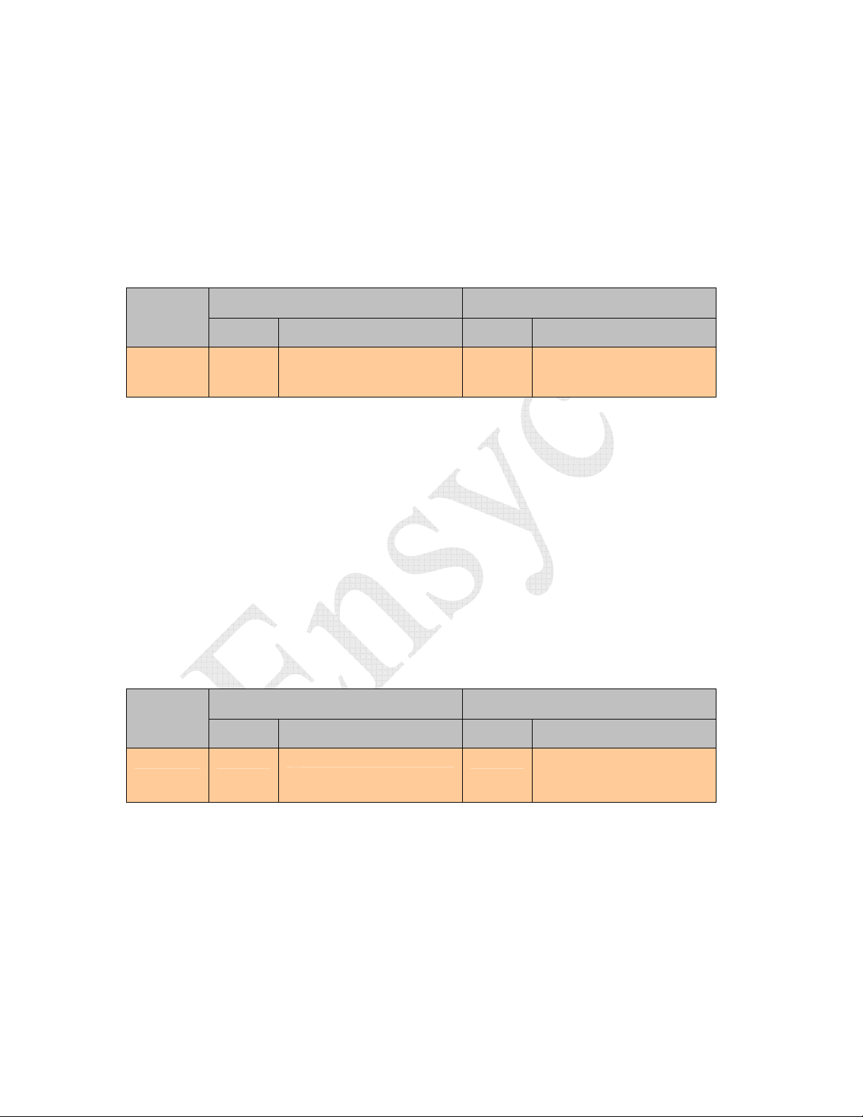
5.1.2.5 Get Reader Status (0x0F)
This command returns operating status information from the reader. The sensor status
returns the state of the optical sensor indicating the presence of a tag for subsequent
RFID interrogation.
Command
Code
Size Valid Values Size Valid Values
Command Data Response Date
0x0F 1 Bytes
0x00 General Status
0x10 Get Sensor Status
1 Byte 0x01 Tag Present (Reflection)
Table 5-9 Get Reader Status
Note: When getting general status, if the EEPROM log is full, the Mtype returned will be
0x98 (LOGFULL).
COMMAND DLE SOM SesID Rdr# Cmd Sub Rpt CRCH CRCL DLE EOM
10 01 01 FF 0F 10 10 3D F7 10 02
RESPONSE DLE SOM SesID Rdr# Echo Mtype Data CRCH CRCL DLE EOM
10 01 01 FF 0F 00 01 BF 73 10 02
Get Sensor Status Example (with reflection)
________________________________________________________________________
Ensyc
- C
Technologies P
ONFIDENTIAL
AGE
18 11:56:13 AM
- M
ARCH
30, 2008
Page 28

RFID UHF Short Range Controller (RF2400)
__________________________________________________________________________
5.1.2.6 Get Reader Hardware Information (0x11)
The Get Reader Hardware Information command provides a mechanism for the host to
identify various aspects of the hardware. Command Data values are used to select
specific parameters.
Command
Code
0x11
Command Data Response Date
Size Valid Values Size Valid Values
1 Byte 0x01 – Get Bidirectional ports (1) 1 Byte
1 Byte 0x02 – Get Flags
1 Byte 0x05 – Get Reader Type (1) 1 Byte
1 Byte 0x06 – Localization Code (1) 1 Byte
1 Byte 0x07 – Radio Type (1) 1 Byte
1 Byte 0x11 -- Tag Class 1 Byte
1 Byte 0x17 – Paper Sensor Trigger 1 Byte
1 Byte 0x18 – Get TagID & Raw ID Retries 1 Byte TagID & Raw ID -- # of Retries
1 Byte 0x20 – Get Tx power step 0
1 Byte 0x21 – Get Tx power step 1 2 Bytes
1 Byte 0x22 – Get Tx power step 2 2 Bytes
1 Byte 0x23 – Get Tx power step 3 2 Bytes
1 Byte 0x24 – Get Receive threshold 1 Byte
1 Byte
2 Bytes
Bitmap:
bit 0 -- port 0
bit 1 -- port 1
bit N – port N
0= not-existent -- 1= exists
Bitmap
Bit 0 = ignore host command CRC
Reader Type
0x09 -- Single RFID Reader
Localization Code
0x01 -- USA
0x02 -- Japan
0x03 -- E.U.
Upper Nibble -- # of Antennas
0x0X -- One Antenna
Lower Nibble – Frequency Band
0xX1 -- 868MHz
0xX2 -- 915MHz
0xX3 -- 950MHz
Bitmap:
bit 0 – Class1
bit 1 – Gen2
Bitmap:
bit 0 – enabled
bit 1 – 0=reflection, 1=no reflection
bit 3 – persistent
Bit 4 – use switch instead of sensor
Bit 5 – store ID in EEPROM
0x00 – 0xFF
Tx power
Tx power
Tx power
Tx power
Receive threshold
Table 5-10 Get Reader Hardware Information
(1) These commands are not currently implemented (unknown value Message Type returned)
________________________________________________________________________
Ensyc
- C
Technologies P
ONFIDENTIAL
AGE
19 11:56:13 AM
- M
ARCH
30, 2008
Page 29

RFID UHF Short Range Controller (RF2400)
__________________________________________________________________________
5.1.2.7 Set Reader Hardware Information (0x13)
The Set Reader Hardware Information command provides a mechanism for the host to
establish various aspects of the hardware. Command Data values are used to select
specific parameters.
Command
Code
0x13
Command Data Response Date
Size Byte Valid Values Size Valid Values
2 Byte 1st
1 Byte 1st 0x06 – Localization Code (2) 1 Byte Reader Type
1 Byte 1st 0x07 – Radio Type (2) 1 Byte Upper Nibble -- # of Antennas
2 Bytes 1st
2 Bytes 1st
2 Bytes 1st
3 Bytes 1st
3 Bytes 1st
3 Bytes 1st
3 Bytes 1st
2 Bytes 1st
0x02 – Set Flags
2nd
Bitmap
Bit 0 – set to ignore host cmd CRC
0x11 – Tag Class
2nd
Bitmap:
bit 0 – Class1
bit 1 – Gen2
Both set = auto detect
0x17 – Paper Sensor Trigger
2nd
Pstrs Bitmap:
bit 0 – enable
bit 1 – 0= reflection, 1= no reflection
bit 2 – is ignored
bit 3 – persistent
bit 4 – use switch instead of sensor
bit 5 – Store ID in EEPROM
0x18 – Set TagID & Raw ID Retries
2nd
# Retries
0x20 – Set Tx power step 0
2,3
Tx power
0x21 – Set Tx power step 1
2,3
Tx power
0x22 – Set Tx power step 2
2,3
Tx power
0x23 – Set Tx power step 3
2,3
Tx power
0x24 – Set Receive Threshold
2nd
Threshold [102 (0x66) = 75mV]
0 Bytes
0x09 -- Single RFID Reader
0x0X -- One Antenna
Lower Nibble – Frequency Band
0xX1 -- 868MHz
0xX2 -- 915MHz
0xX3 -- 950MHz
0 Bytes --
0 Bytes --
0 Bytes Def = 7--
0 Bytes
0 Bytes
0 Bytes
0 Bytes
0 Bytes
Table 5-11 Set Reader Hardware Information
(2) These commands are not yet implemented (unknown value Message Type returned)
COMMAND DLE SOM SesID Rdr# Cmd Sub Data CRCH CRCL DLE EOM
10 01 01 FF 13 02 01 5E 62 10 02
RESPONSE DLE SOM SesID Rdr# Echo Mtype CRCH CRCL DLE EOM
10 01 01 FF 13 00 xx xx 10 02
Set Reader Hardware Example (Ignore CRC)
________________________________________________________________________
Ensyc
- C
Technologies P
ONFIDENTIAL
AGE
20 11:56:13 AM
- M
ARCH
30, 2008
Page 30

RFID UHF Short Range Controller (RF2400)
__________________________________________________________________________
5.1.2.7.1 Paper Sensor Triggered Read
The paper sensor triggered read (PSTR) mode can be set-up and enabled using the “Set
Hardware Information” command, sub-command 0x17. This mode is used to enable
automatic tag reading based on the state of the optical reflection sensor. Using this
command, triggered reading can be enabled or disabled, set to operate in host or service
port mode, based on reflection or no reflection and set to persist over power cycling. The
triggered read state (pstrs) is set using the data byte following the sub-command. The bit
definitions for pstrs follow:
Bit 0 enables or disables triggered reads where a one (1) indicates triggered read is
enabled and a zero (0) indicates disabled.
Bit 1 indicates which optical state is used to trigger a read where one (1) triggers the
read on a no reflection and a zero (0) triggers the read on reflection. This bit is
ignored when a switch is used in place of the optical sensor(bit 4 is set to a 1)
Bit 2 is reserved and is ignored. (used internally to indicate host vs SP mode)
Bit 3 establishes if the state persists over power cycles where a one (1) indicates the
state persists over a power cycle and a zero (0) indicates that the state does not
persist.
Bit 4 set to one (1) indicates a switch is used instead of the sensor for triggering. When
Bit 5 determines whether the ID data are returned or stored. A zero (0) indicates to
the switch contacts are closed the state is triggered.
return the ID data immediately, while a one (1) causes the data to be stored in
EEPROM for future retrieval. Refer to the “Dump ID Data” command. Bad
reads are not stored in EEPROM.
When the PSTR mode is enabled using this host command, the triggered read tag data are
sent as a Binary packet in host mode or saved in EEPROM.
When storing to EEPROM, only good reads are stored. When the EEPROM log is full
(496 records), the PSTR function is terminated. An error message is sent to the host with
the Mtype set to 0x98 (LOGFULL).
Note: To use a switch in place of the paper sensor, wire between J3 pins 1 and 2.
________________________________________________________________________
Ensyc
- C
Technologies P
ONFIDENTIAL
AGE
21 11:56:13 AM
- M
ARCH
30, 2008
Page 31
RFID UHF Short Range Controller (RF2400)
__________________________________________________________________________
5.1.2.8 Set Bi-Directional I/O DDR (0x16)
The data byte of this command defines the two bi-directional ports on the RF2400 as
either inputs or outputs. The command data is saved in non-volatile memory and
preserves the port definition through power interruptions. The LSB of the data byte
controls port 0 and bit 1 controls port 1. A logic one defines a port as an input while a
logic zero defines a port as an output. The factory default for the control byte is 0xFF
setting both IO pins as inputs
Command
Code
0x16 1 Byte
Size Valid Values Size Valid Values
Command Data Response Date
Bitmap:
0 = output
1 = input
0 Bytes --
Table 5-12 Set Bi-Directional I/O DDR
COMMAND DLE SOM SesID Rdr# Cmd Data CRCH CRCL DLE EOM
10 01 01 FF 16 02 D2 76 10 02
RESPONSE DLE SOM SesID Rdr# Echo Mtype CRCH CRCL DLE EOM
10 01 01 FF 16 00 F2 34 10 02
Set Bi-Directional I/O DDR Example
Note: Set Bi-Directional I/O DDR must be executed for the IO pin to be valid. This example Sets port 0 as an input and port
1 as an output
5.1.2.9 Get Bi-Directional I/O DDR (0x17)
This command returns the data byte defining the bi-directional IO ports
Command
Code
0x17 0 Bytes
Size Valid Values Size Valid Values
Command Data Response Date
--
1 Byte Bitmap:
0 = output
1 = input
Table 5-13 Get Bi-Directional I/O DDR
COMMAND DLE SOM SesID Rdr# Cmd CRCH CRCL DLE EOM
10 01 01 FF 17 36 DA 10 02
RESPONSE DLE SOM SesID Rdr# Echo Mtype Data CRCH CRCL DLE EOM
10 01 01 FF 17 00 02 89 67 10 02
Get Bi-Directional I/O DDR Example
Note: this example assumes that the Set Bi-Directional I/O DDR has been executed.
________________________________________________________________________
Ensyc
- C
Technologies P
ONFIDENTIAL
AGE
22 11:56:13 AM
- M
ARCH
30, 2008
Page 32

RFID UHF Short Range Controller (RF2400)
__________________________________________________________________________
5.1.3 Tag Commands
Tag type commands result in the RF2400 reader sending commands to a tag by
modulating the RF carrier. Tags may respond by modulating the RF backscatter.
5.1.3.1 Sleep Tag (0x21)
This command issues an air interface SLEEP command…..(3)
Command
Code
0x21 0 Bytes
Size Valid Values Size Valid Values
Command Data Response Date
--
0 Bytes --
Table 5-14 Sleep Tag
(3) This command is not yet implemented (unknown value Message Type returned)
5.1.3.2 Get Tag ID (0x24)
This low-level command issues the required air interface commands to acquire one tag
ID. CRC checking is enforced and a Good ID Tag Decode Status is only available if the
CRC is validated. An ID response is only returned for a Good ID Decode status and
begins with two bytes of CRC followed by either eight or twelve bytes of ID data. The
LOCK and KILL fields are not included in the tag response data.
Class 1 tags are interrogated for both 64-bit and 96-bit standards. The CRC is initially
calculated over the first eight bytes and over twelve bytes if the eight byte calculation
fails. The Tag Data Length indicator identifies which CRC evaluated correctly
Command
Code
Size Valid Values Size Valid Values
Command Data Response Date
0x24 0 Bytes
--
N Bytes Tag Type Specific
Table 5-15 Get Tag ID
COMMAND DLE SOM SesID Rdr# Cmd CRCH CRCL DLE EOM
10 01 01 FF 24 30 EA 10 02
RESPONSE DLE SOM SesID Rdr# Echo Mtype Tsts Ant# Len tCRCH tCRCL
10 01 01 FF 24 00 00 00 0E 89 7C
TAG ID CRCH CRCL DLE EOM
01 02 03 04 05 06 07 08 09 0A 0B 0C E6 16 10 02
Get Tag ID Example
Note: this example assumes that the Program Tag example has been executed and both commands execute with success.
________________________________________________________________________
Ensyc
- C
Technologies P
ONFIDENTIAL
AGE
23 11:56:13 AM
- M
ARCH
30, 2008
Page 33

RFID UHF Short Range Controller (RF2400)
__________________________________________________________________________
5.1.3.3 Auto Get Tag ID (0x26)
This low-level command issues the required air interface commands to repeatedly acquire
tag IDs. A response message is sent for each read, the format of which is identical to the
Get Tag ID command. A delay may be introduced between reads in 10ms increments.
The Dly byte follows the Cmd byte. Each read with the delay of 0 consumes
approximately 43mS. The operation repeats indefinitely until any other command is
executed.
A flag byte (Flg) allows setting options as follows:
Bit 0 = 1 Enables retries.
Bit 1 = 1 Store ID in EEPROM vs. send to host.
The retry count is set with the “Set Reader Hardware Information” command, Set Tag ID
& Raw ID retries with a default value of 7. With retries enabled and a count of 7 and no
tag present, a total of 16 reads are done which includes 8 for each of the two RF phases.
This consumes 688 mS plus any delay count. If auto class detect is enabled, this time is
doubled. Auto Class Detect should be disabled, set TC=2 for Gen2.
When storing to EEPROM, only good reads are stored. When the EEPROM log is full
(496 records), the Auto Get Tag ID function is terminated. A message is sent to the host
with the Mtype set to 0x98 (LOGFULL).
CRC checking is enforced and a Good ID Tag Decode Status is only available if the CRC
is validated. An ID response is only returned for a Good ID Decode status and begins
with two bytes of CRC followed by either eight or twelve bytes of ID data. The LOCK
and KILL fields are not included in the tag response data.
Class 1 tags are interrogated for both 64-bit and 96-bit standards. The CRC is initially
calculated over the first eight bytes and over twelve bytes if the eight byte calculation
fails. The Tag Data Length indicator identifies which CRC evaluated correctly
Command
Code
0x26 2 Bytes
Size Valid Values Size Valid Values
Command Data Response Date
1st Byte--Delay in 10mS 0x00 to 0xFF2nd Byte—Flags
.....Bit 0 = 1 enable retries
…..Bit 1 = 1 store IDs in EEPROM
N Bytes Tag Type Specific
Table 5-16 Auto Get Tag ID
COMMAND DLE SOM SesID Rdr# Cmd Dly Flg CRCH CRCL DLE EOM
10 01 01 FF 26 25 01 72 8D 10 02
RESPONSE DLE SOM SesID Rdr# Echo Mtype Tsts Ant# Len tCRCH tCRCL
10 01 01 FF 26 00 00 00 0E 89 7C
TAG ID CRCH CRCL DLE EOM
01 02 03 04 05 06 07 08 09 0A 0B 0C 1E A1 10 02
Auto Get Tag ID Example
Note: this example assumes that the Program Tag example has been executed and both commands execute with success.
________________________________________________________________________
Ensyc
- C
Technologies P
ONFIDENTIAL
AGE
24 11:56:13 AM
- M
ARCH
30, 2008
Page 34

RFID UHF Short Range Controller (RF2400)
__________________________________________________________________________
5.1.3.4 Dump ID Data (0x28)
This command returns ID data that has been stored in EEPROM.
The Length byte indicates the number of records to return (max 16). An internal pointer
tracks records sent so that a repeat of this command can fetch the next group of records.
The data dump will stop when a zeroed record is encountered (end of stored data). A
response is sent with the length indicating the number of records that were returned.
The imbedded EEPROM (8Kx8) can store 496 entries.
Command
Code
0x28 2 Bytes
Size Valid Values Size Valid Values
Command Data Response Date
1st Byte—Subcmd
0x01 Dump after reset pointer
0x02 Dump using current pointer
0x03 Get number of records
stored
0x04 Clear all records
2nd Byte— Length in records 0x00 to
0x10
2 Bytes Number of records H/L byte
Table 5-17 Dump ID Data Command
COMMAND DLE SOM SesID Rdr# Cmd Sub Len CRCH CRCL DLE EOM
10 01 01 FF 28 01 01 E7 23 10 02
RESPONSE DLE SOM SesID Rdr# Echo Mtype SeqH SeqL# Len tCRCH tCRCL
10 01 01 FF 02 00 00 00 0E 89 7C
TAG ID CRCH CRCL DLE EOM
01 02 03 04 05 06 07 08 09 0A 0B 0C 85 71 10 02
RESPONSE DLE SOM SesID Rdr# Echo Mtype LenH LenL CRCH RPT CRCL DLE EOM
10 01 01 FF 28 00 00 01 10 10 64 10 02
Dump ID Data Example (Single Record)
Note: at least one record must have been previously stored in memory using SP mode
Paper Sensor Triggered Read
The Dump Record indicates the stored record number in SeqH/SeqL. The Echo byte
indicates which command stored this record as follows:
0x01 SP_ART SP mode Auto Read Tag
0x02 SP_PSTR SP mode Paper Sensor Triggered Read
0x11 H_PSTR Host mode Paper Sensor Triggered Read
0x26 H_AUTO Host mode Auto Get Tag ID
________________________________________________________________________
Ensyc
- C
Technologies P
ONFIDENTIAL
AGE
25 11:56:13 AM
- M
ARCH
30, 2008
Page 35

RFID UHF Short Range Controller (RF2400)
__________________________________________________________________________
5.1.3.5 Get Raw Tag ID (0x3E)
This low-level command issues the required air interface commands to acquire one tag
ID without CRC checking. Response data varies in length and is specific to tag class.
Class 1 tags return a tag data length of 12 or 16. The response begins with two bytes of
CRC followed by either eight or twelve bytes of ID, a one byte kill code and ends with a
one byte lock code.
Gen 2 returns a tag ID length of 22. The response begins with two bytes of CRC
followed by twelve bytes of ID, a four byte kill password, and a four byte access
password. Although the Gen2 specification defines long EPC codes the RF2400 only
supports a 96-bit EPC. IF the kill password is read/write locked the password will be
returned as zeros (note: an all zero kill password is illegal).
The Tag Decode Status provides success or failure status for the command in addition to
other status indicators. If the command was successful bits 0-3 will all be zero. A binary
code of three in these bits indicates a CRC error. For a Class 1 tag, if Bits 4 & 5 are both
set, the tag is locked. For a Gen 2 tag, if Bit 4 in the Tag Decode status is set, the Kill
Password is locked and if Bit 5 in the Tag Decode status is set, the Access Password is
locked.
Command
Code
0x3E 0 Bytes
Size Valid Values Size Valid Values
Command Data Response Date
12/16 Bytes
-22 Bytes
Class 1 Tag
CRC (2-bytes)
….ID (8 or 12 bytes)
Kill Code (1-byte)
Lock Code (1-byte)
Class 2 Tag
CRC (2-bytes)
ID (12-bytes)
Kill Password (4-bytes)
Access Password (4-bytes)
Table 5-18 Get Raw Tag ID
COMMAND DLE SOM SesID Rdr# Cmd CRCH CRCL DLE EOM
10 01 01 FF 3E 83 91 10 02
RESPONSE DLE SOM SesID Rdr# Echo Mtype Tsts Ant# Len tCRCH tCRCL
10 01 01 FF 3E 00 00 00 16 89 7C
TAG ID
01 02 03 04 05 06 07 08 09 0A 0B 0C
Kill Password Access Password CRCH CRCL DLE EOM
00 00 00 00 00 00 00 00 86 21 10 02
Get Raw Tag ID (Gen2) Example
Note: this example assumes that the Program Tag example has been executed and both commands execute with success.
________________________________________________________________________
Ensyc
- C
Technologies P
ONFIDENTIAL
AGE
26 11:56:13 AM
- M
ARCH
30, 2008
Page 36

RFID UHF Short Range Controller (RF2400)
__________________________________________________________________________
5.1.3.6 Program Tag (0x50)
The Program Tag command writes data to the tag ID. The command includes: four
control parameters and the ID data. The first three parameters (find tag retries, erase
retries, and program retries) establish retry counters for detecting the presence of a tag,
erasing the tag and finally programming the tag. The RF2400 only supports tags written
in 96 bit format. Correspondingly, the only valid ID length is twelve (0x0C) and must
match the number of ID data bytes in the command. If the Tag is Class 1, A CRC (
CCITT-16
) is generated for the 96-bits of ID data and programmed into the first two bytes
CRC-
in tag memory followed by the ID data. This command does not write the LOCK or
KILL bytes.
If successful, a MSGOK will be returned otherwise an error code indicating the failure
will be returned. Error codes (
CommCode
) include HWERR, UNKTAGCMD,
UNKIDLEN NOTAG, ERASEFAIL, PROGFAIL, TAGLOST, and TAGLOCK. If the
Mtype field in the response is non-zero, an error has occurred, and the tag must be
considered invalid.
Command
Code
0x50 16 Bytes
Size Valid Values Size Valid Values
Command Data Response Date
1st Byte—Find Tag retries 0x00-0xFF
2nd Byte--Erase retries 0x00-0xFF
3rd Byte--Program retries 0x00-0xFF
4th Byte—ID Length 0x0C
5th -16th Bytes—ID Data (12 Bytes)
0 Bytes --
Table 5-19 Program Tag
COMMAND DLE SOM SesID Rdr# Cmd Xrty Erty Wrty Len
10 01 01 FF 50 7 7 7 0C
Tag ID CRCH CRCL DLE EOM
01 02 03 04 05 06 07 08 09 0A 0B 0C 84 33 10 02
RESPONSE DLE SOM SesID Rdr# Echo Mtype CRCH CRCL DLE EOM
10 01 01 FF 50 00 5D 39 10 02
Program Tag Example
Note: this example assumes that the command executes successfully.
________________________________________________________________________
Ensyc
- C
Technologies P
ONFIDENTIAL
AGE
27 11:56:13 AM
- M
ARCH
30, 2008
Page 37

RFID UHF Short Range Controller (RF2400)
__________________________________________________________________________
5.1.3.7 Erase Tag (0x51)
The Erase Tag command erases and verifies the tag was properly erased. The command
begins with a tag search which repeats up to the given number of find tag retries or until
a valid tag is found. Subsequently, the Erase command is iterated up to the number of
times defined by erase retries or until the erase is verified. A Class 1 tag is written with
both the CRC and ID data set to zero. A Gen2 tag is written with only the ID data set to
zero since the CRC is calculated by the tag. A successful operation is determined if the
tag ID is erased to all zeros for both Class 1 and Gen2 tags and in addition the CRC is set
to zero for a Class 1 tag.
If successful a MSGOK will be returned otherwise an error code indicating the failure
will be returned. Error codes (
CommCode
) include HWERR, UNKTAGCMD, NOTAG,
ERASEFAIL, TAGLOST, and TAGLOCK.
Command
Code
0x51 2 Bytes
Size Valid Values Size Valid Values
Table 5-20 Erase Tag
Command Data Response Date
1st Byte—Find Tag Retries 0x000xFF
2nd Byte--Erase retries 0x00-0xFF
0 Bytes --
________________________________________________________________________
Ensyc
- C
Technologies P
ONFIDENTIAL
AGE
28 11:56:13 AM
- M
ARCH
30, 2008
Page 38

RFID UHF Short Range Controller (RF2400)
__________________________________________________________________________
5.1.3.8 Kill Tag (0x52)
This command permanently erases or deactivates and verifies that all tag data has been
erased or will no longer respond to or execute reader commands. The command begins
with a tag search which repeats up to the given number of find tag retries or until a valid
tag is found. Subsequently, the Kill function is iterated up to the number of times defined
by kill retries or until the Kill is verified. The RF2400 only supports tags written in 96
bit format thus the only valid ID length is twelve (0x0C). For Class 1 tags the calculated
CRC (
CRC-CCITT-16
) along with the provided, ID data, and kill code must match the
corresponding tag data for the kill operation to complete. For a Gen2 tag the 4-byte kill
password mush match the tags kill password. A successful operation is determined if all
tag data has been erased or the tag will no longer responds to reader commands.
If successful a MSGOK will be returned otherwise an error code indicating the failure
will be returned. Error codes (
CommCode
) include HWERR, UNKTAGCMD, NOTAG,
DATASIZE, TAGLOST, TAGLOCK and KILLFAIL.
Command
Code
0x50 19 Bytes
Size Valid Values Size Valid Values
Table 5-21 Kill Tag
Command Data Response Date
1st Byte—FindTag Retries 0x00-0xFF
2nd Byte--Kill retries 0x00-0xFF
3rd Byte—ID Length 0x0C
4th -15th Bytes
Class 1 -- 12-bytes ID Data
Gen2 -- Ignored
16th -19th Bytes
Class 1 (first byte only)
KILL code
0x00-0xFF
Gen2 (all four bytes)
kill password
0x00000000 – 0xFFFFFFFF
0 Bytes --
________________________________________________________________________
Ensyc
- C
Technologies P
ONFIDENTIAL
AGE
29 11:56:13 AM
- M
ARCH
30, 2008
Page 39

RFID UHF Short Range Controller (RF2400)
__________________________________________________________________________
5.1.3.9 Lock Tag (0x53)
The LOCK command sets and verifies the tag kill code. For Class 1 tags the lock code
[0xA5] is also verified (Gen 2 has no lock code). This establishes the tag kill code and
locks the tag preventing any further modification of the tag ID, or CRC. The command
begins with a tag search which repeats up to the given number of find tag retries or until
a valid tag is found. Subsequently, the Lock command is iterated up the number of lock
retries or for Class 1 until the tag read response consists of only the CRC followed by the
12 bytes of Tag ID data indicating LOCK is verified. Note the kill code and lock code
are not backscattered on locked Class 1 tags. For Gen 2 tags after the kill password is
written both the EPC and kill password are locked and the tag response indicates success
or failure which verifies the LOCK. Note the kill password is not backscattered on locked
Gen2 tags. Since The RF2400 only supports tags written in 96 bit format, the only valid
ID length is twelve (0x0C). Additionally, the lock command will only function on tags
previously written in a 96-bit format having an IDLEN of 12 bytes. A successful
operation is determined if LOCK is verified.
If successful a MSGOK will be returned otherwise an error code indicating the failure
will be returned. Error codes (
CommCode
) include HWERR, UNKTAGCMD, NOTAG,
DATASIZE, TAGLOST, TAGLOCK, and LOCKFAIL.
Command
Code
0x50 7 Bytes
Table 5-22 Lock Tag
Command Data Response Date
Size Valid Values Size Valid Values
1st Byte—Tag Retries 0x00-0xFF
2nd Byte--Lock attempts 0x01-0xFF
3rd Byte-- ID Length 0x0C
4th – 7th Bytes
Class 1 (first byte only)
KILL code
0x00-0xFF
Gen2 (all four bytes)
kill password
0x00000000 – 0xFFFFFFFF
0 Bytes --
________________________________________________________________________
Ensyc
- C
Technologies P
ONFIDENTIAL
AGE
30 11:56:13 AM
- M
ARCH
30, 2008
Page 40

RFID UHF Short Range Controller (RF2400)
__________________________________________________________________________
5.1.3.10 Program Tag Init (0x54)
This variant of the Program Tag command writes 0x3000 to the PC (protocol control)
field, and then continues to write data to the tag ID. This sets up an un-initialized tag for
a 96 bit EPC. The command includes: four control parameters and the ID data. The first
three parameters (find tag retries, erase retries, and program retries) establish retry
counters for detecting the presence of a tag, erasing the tag and finally programming the
tag. The RF2400 only supports tags written in 96 bit format. Correspondingly, the only
valid ID length is twelve (0x0C) and must match the number of ID data bytes in the
command. If the Tag is Class 1, A CRC (
CRC-CCITT-16
) is generated for the 96-bits of
ID data and programmed into the first two bytes in tag memory followed by the ID data.
This command does not write the LOCK or KILL bytes.
If successful a MSGOK will be returned otherwise an error code indicating the failure
will be returned. Error codes (
CommCode
) include HWERR, UNKTAGCMD,
UNKIDLEN NOTAG, ERASEFAIL, PROGFAIL, TAGLOST, and TAGLOCK. If the
Mtype field in the response is non-zero, an error has occurred, and the tag must be
considered invalid.
Command
Code
0x54 16 Bytes
Size Valid Values Size Valid Values
Command Data Response Date
1st Byte—Find Tag retries 0x00-0xFF
2nd Byte--Erase retries 0x00-0xFF
3rd Byte--Program retries 0x00-0xFF
4th Byte—ID Length 0x0C
5th -16th Bytes—ID Data (12 Bytes)
0 Bytes --
Table 5-23 Program Tag Init
COMMAND DLE SOM SesID Rdr# Cmd Xrty Erty Wrty Len
10 01 01 FF 54 7 7 7 0C
Tag ID CRCH CRCL DLE EOM
01 02 03 04 05 06 07 08 09 0A 0B 0C 2D 84 10 02
RESPONSE DLE SOM SesID Rdr# Echo Mtype CRCH CRCL DLE EOM
10 01 01 FF 54 00 81 F9 10 02
Program Tag Init Example
Note: this example assumes that the command executes successfully.
________________________________________________________________________
Ensyc
- C
Technologies P
ONFIDENTIAL
AGE
31 11:56:13 AM
- M
ARCH
30, 2008
Page 41

RFID UHF Short Range Controller (RF2400)
__________________________________________________________________________
5.1.3.11 LockG2 (0x55)
The LOCKG2 command is specifically used with Gen 2 tags. It allows locking of
individual passwords and memory banks. The lock status for a password or memory bank
can be Perma-locked (making it permanently unchangeable). The command begins with
a tag search which repeats up to the given number of find tag retries or until a valid tag is
found. Subsequently, the Lock command is iterated up the number of lock retries. The
Data Length of 8 indicates that following are 4 byte Access Password, 2 byte Mask and 2
byte Action field. The Access Password supplied must match that of the tag’s otherwise
the command will fail with a TAGLOST response. If an Access Password has not been
written to the tag, it defaults to 00000000.
Note: If the access password is not zero, tag writes will be done from the OPEN state,
not the SECURED state. There are 2 methods that can be used to write. First: a locked
tag may be unlocked by clearing the PWD bit using the LOCKG2 command before
attempting to write, Second: Enter the access password with the Access command to
cause transition from OPEN to SECURED state for reads and writes. The LOCKG2
command does transition from OPEN to SECURED using the supplied password.
If the tag’s access password is zero, the tag never enters the OPEN state, but goes directly
to the SECURED state.
Use the Write Tag Memory command to write passwords to the tag. Refer to section
5.4.1.
If successful a MSGOK will be returned otherwise an error code indicating the failure
will be returned. Error codes (
CommCode
) include HWERR, UNKTAGCMD, NOTAG,
DATASIZE, TAGLOST, TAGLOCK, and LOCKFAIL.
Command
Code
0x55 11 Bytes
Size Valid Values Size Valid Values
Command Data Response Date
1st Byte—Tag Retries 0x00-0xFF
2nd Byte--Lock attempts 0x01-0xFF
3rd Byte-- Data Length 0x08
4th – 7th Bytes—Access Password
8th – 9th Bytes—10 bit Mask
10th – 11th Bytes—10 bit Action
0 Bytes --
Table 5-24 LockG2
COMMAND DLE SOM SesID Rdr# Cmd Xrty Erty Len
10 01 01 FF 55 07 07 08
Access Password MaskH MaskL ActionH ActionL CRCH CRCL DLE EOM
01 02 03 04 00 20 00 20 2F 4E 10 02
RESPONSE DLE SOM SesID Rdr# Echo Mtype CRCH CRCL DLE EOM
10 01 01 FF 55 00 B6 C9 10 02
LockG2 Example (Lock EPC)
Note: this example assumes that the command executes successfully.
________________________________________________________________________
Ensyc
- C
Technologies P
ONFIDENTIAL
AGE
32 11:56:13 AM
- M
ARCH
30, 2008
Page 42
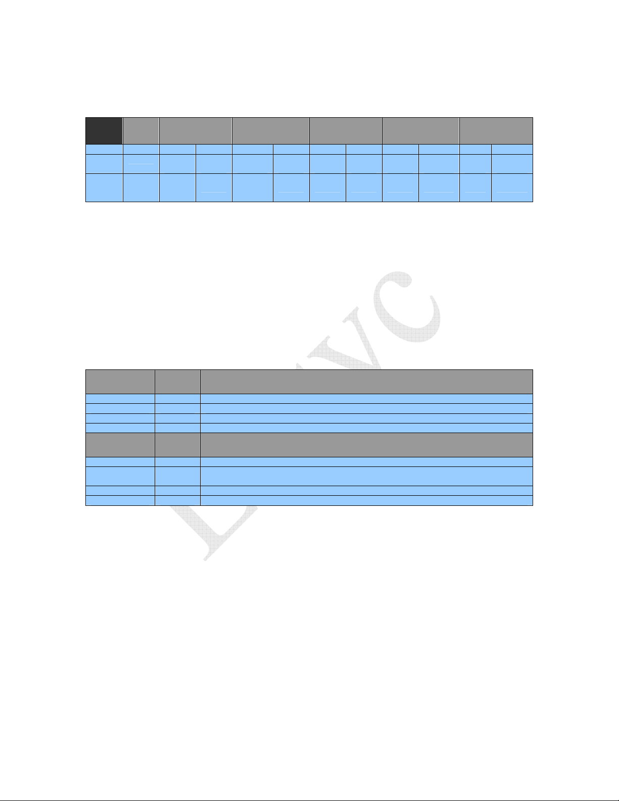
RFID UHF Short Range Controller (RF2400)
__________________________________________________________________________
Lock contains two 10 bit fields, a mask and action, each sent as two bytes with the upper
6 bits of the high byte not used. The high byte (bits 15-8) is sent first.
Field
bit 15 - 10 9 8 7 6 5 4 3 2 1 0
mask
action
Not
used
Skip/
Pwd
Kill
password
write
Read/
write
Skip/
write
Perma
lock
Access
password
Skip/
write
Pwd
Read/
write
Skip/
write
Perma
lock
EPC
memory
Skip/
write
Pwd
write
Skip/
write
Perma
lock
TID
memory
Skip/
write
Pwd
write
Skip/
write
Perma
lock
User
memory
Skip/
write
Pwd
write
Skip/
write
Perma
lock
Table 5-25 Lock bit usage
Bit function is as follows:
Mask = 0: Ignore the associated action field and retain the current lock setting..
Mask = 1: Implement the associated action field and overwrite the current lock
setting.
Action = 0: Deassert lock for the associated field.
Action = 1: Assert lock or perma-lock for associated field.
Note: Perma-lock bits, once asserted, cannot be deasserted.
Pwd-write Perma-
lock
0 0 Bank is writable from either the OPEN or SECURED state.
0 1 Bank is permanently writable from either the OPEN or SECURED state.
1 0 Bank is writeable from the SECURED state but not from the OPEN state.
1 1 Bank is not writable from any state.
Pwdread/write
0 0 Password is readable and writeable from either the OPEN state or the SECURED state.
0 1 Password is permanently readable and writeable from either the OPEN or the SECURED
1 0 Password is writeable from the SECURED state but not from the OPEN state.
1 1 Password is not readable or writable from any state.
Permalock
Description
Description
state.
Table 5-26 Lock action field functionality
________________________________________________________________________
Ensyc
- C
Technologies P
ONFIDENTIAL
AGE
33 11:56:13 AM
- M
ARCH
30, 2008
Page 43
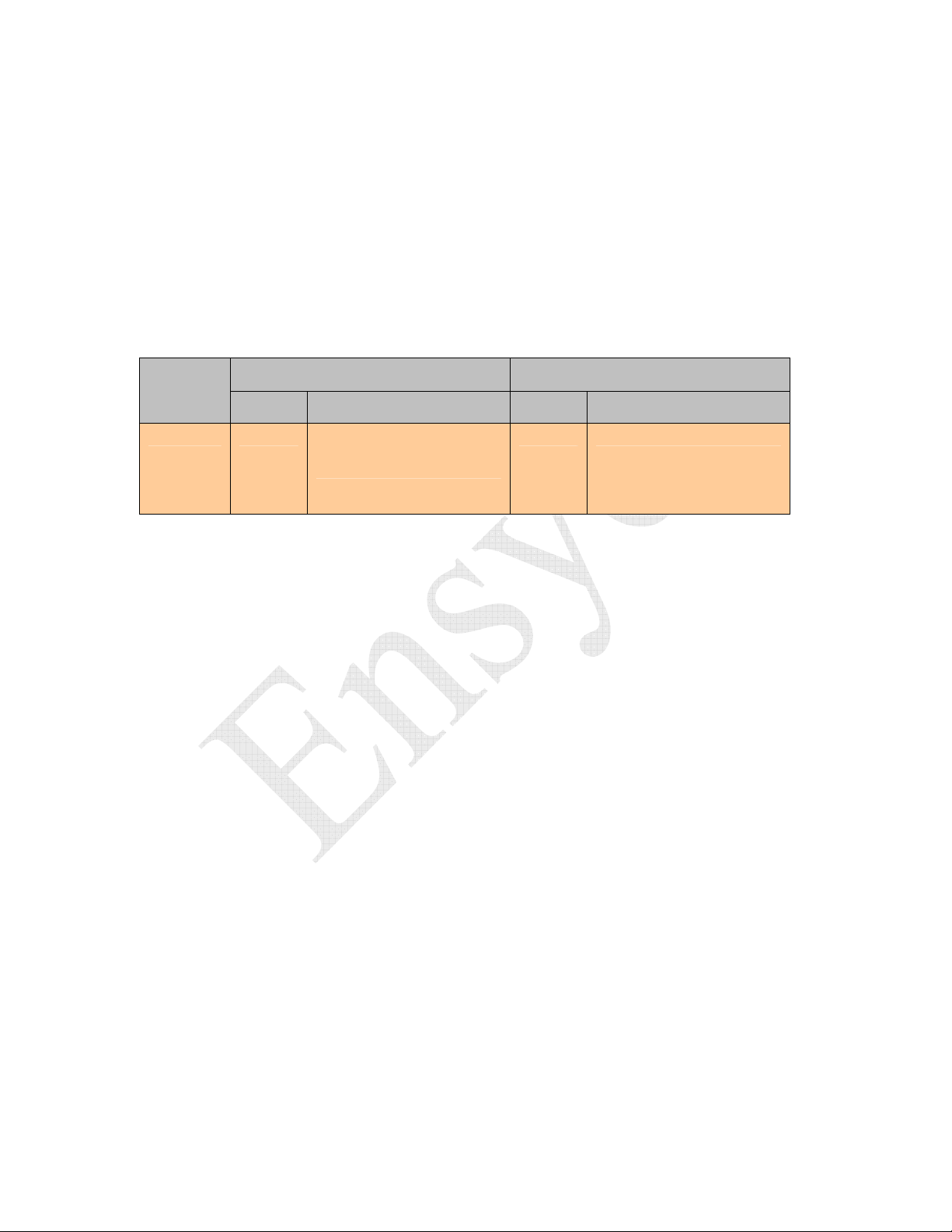
RFID UHF Short Range Controller (RF2400)
__________________________________________________________________________
5.1.3.12 Access G2 (0x56)
The Access command allows entry of an Access password for communication with GEN
2 Tags. This command does not communicate with the tag.
If the tag’s access password is zero, the tag never enters the OPEN state, but goes directly
to the SECURED state and this command is not needed.
If the tag’s access password is non-zero, the tag enters the OPEN state. The password
entered with this command is used to bring the tag to the SECURED state, allowing
writes to an area that is non-perma locked.
Command
Code
0x56 5 Bytes
Size Valid Values Size Valid Values
Command Data Response Date
1st Byte—Data Length 0x04
2nd – 5th Byts-- Access Password
Table 5-27 AccessG2
COMMAND DLE SOM SesID Rdr# Cmd Len
10 01 01 FF 56 04
Access Password CRCH CRCL DLE EOM
01 02 03 04 67 6C 10 02
RESPONSE DLE SOM SesID Rdr# Echo Mtype CRCH CRCL DLE EOM
10 01 01 FF 56 00 EF 99 10 02
AccessG2 Example
0 Bytes --
________________________________________________________________________
Ensyc
- C
Technologies P
ONFIDENTIAL
AGE
34 11:56:13 AM
- M
ARCH
30, 2008
Page 44

RFID UHF Short Range Controller (RF2400)
__________________________________________________________________________
5.1.3.13 Read Tag Memory (0x57)
The Read Tag Memory command allows an interrogator to read from 1 to 16 words from
a Tag’s Reserved, EPC, TID or User memory. Read Tag Memory has the following
fields:
• Bank - Bits 7,6 of Extent select Reserve, EPC, TID, or User memory.
• Length - Bits 5-0 of Extent indicates the number of bytes to write.
• Address - Indicates the word offset within the bank.
For Tag memory layout information please see Table 5-42
Although the length is specified in bytes (counts bytes transferred across the serial
interface), the Tag memory is accessed in words. The length supplied must be even or
else an error is returned. The maximum length supported is 16 bytes (8 words). If a
larger number is requested, an error will be returned. The maximum address supported is
16383 (14 bits). If a write is attempted to an area not supported by the Tag, an error is
returned. The Read Tag Memory command is only supported for Gen2 tags.
If successful, a MSGOK response is returned, otherwise an error response is given with
the Message Type (CommCode) indicating the failure. Possible CommCodes include
NOTAG, TAGLOST, TAGLOCK, TAGNXM, UNKCMD, and UNKVAL.
Command
Code
0x57 3 Bytes
Size Valid Values Size Valid Values
Command Data Response Date
1st Byte—Extent (bank/length)
2nd/3rd Byte—Word Address H/L
0-16 Bytes Read Data--
Table 5-28 Read Tag Memory
COMMAND DLE SOM SesID Rdr# Cmd Extent AdrH AdrL CRCH CRCL DLE EOM
10 01 01 FF 57 04 00 02 A7 89 10 02
RESPONSE DLE SOM SesID Rdr# Echo Mtype Tsts Ant# Len
10 01 01 FF 57 00 00 00 04
TAG data CRCH CRCL DLE EOM
01 02 03 04 FE 75 10 02
Read Tag Memory Example (read access password)
________________________________________________________________________
Ensyc
- C
Technologies P
ONFIDENTIAL
AGE
35 11:56:13 AM
- M
ARCH
30, 2008
Page 45

RFID UHF Short Range Controller (RF2400)
__________________________________________________________________________
5.1.3.14 Write Tag Memory (0x58)
The Write Tag Memory command allows an interrogator to write from 1 to 8 words to a
Tag’s Reserved, EPC, TID or User memory. Write Tag Memory has the following
fields:
• Bank - Bits 7,6 of Extent select Reserve, EPC, TID, or User memory.
• Length - Bits 5-0 of Extent indicates the number of bytes to write.
• Address - Indicates the word offset within the bank.
• Data - Up to 16 bytes (8 words) to be written.
For Tag memory layout information please see Table 5-42
Although the length is specified in bytes (counts bytes transferred across the serial
interface), the Tag memory is accessed in words. The length supplied must be even or
else an error is returned. The maximum length supported is 16 bytes (8 words). If a
larger number is requested, an error will be returned. The maximum address supported is
16383 (14 bits). If a write is attempted to an area not supported by the Tag, an error is
returned. The Write Tag Memory command is only supported for Gen2 tags.
If successful, a MSGOK response is returned, otherwise an error response is given with
the Message Type (CommCode) indicating the failure. Possible CommCodes include
NOTAG, TAGLOST, TAGLOCK, TAGNXM, UNKCMD, and UNKVAL.
Command
Code
0x58 4-19 Bytes
Size Valid Values Size Valid Values
Command Data Response Date
1st Byte—Extent (bank/length)
rd
2nd/3
Byte—Word Address H/L
3rd – 19th Bytes—Data
0 Bytes --
Table 5-29 Write Tag Memory
COMMAND DLE SOM SesID Rdr# Cmd Extent AdrH AdrL Data CRCH CRCL DLE EOM
10 01 01 FF 58 04 00 02 01 02 03 04 7B 20 10 02
RESPONSE DLE SOM SesID Rdr# Echo Mtype CRCH CRCL DLE EOM
10 01 01 FF 58 00 F4 98 10 02
Write Tag Memory Example (write access password)
________________________________________________________________________
Ensyc
- C
Technologies P
ONFIDENTIAL
AGE
36 11:56:13 AM
- M
ARCH
30, 2008
Page 46

RFID UHF Short Range Controller (RF2400)
__________________________________________________________________________
5.2 SERVICE PORT COMMANDS
In addition to the binary message format, the RF2400 supports an ASCII communication
mode providing a service menu using the existing RS232 interface. The RF2400 powers
up accepting binary messages as described in section 5.1 above and posts a single line
message containing the current version of the firmware. To activate the service menu, it
is necessary to send the proper token lead-in sequence (
5-30. Two sets of commands are available; standard and protected provide user and
factory/service personnel associated command and configuration menus.
Token Description
[DLE][SMR]
) as shown in Table
[DLE]
[SMR]
Data Link Escape token; 0x10
Service mode token; 0x04
(^d)
(^p)
Table 5-30 Service Port Lead-in sequence
5.2.1 Standard Commands
Standard commands are available to all users and are documented in this specification.
These commands provide a means to test the basic operation of the reader and to
configure several operating parameters. Note all operating parameters can be returned
to the factory defaults by installing the jumper JX and powering cycling the board.
5.2.1.1 Baud Rate (baud) command
The baud rate (baud) command allows the user to reconfigure the RS232 interface baud
rate. There are six baud rates available ranging from 9,600 baud to 115200 baud. Baud
rates are represented using a single decimal parameter from 0 to 5: baud 0 = 9600, baud 1
= 19200, baud 2 = 38400, baud 3 =57600, and baud 4 = 115200,. The default RS232
configuration is 19,200 baud using 8 data bits, 1 stop bit, and no parity. The current baud
rate is read using the baud
using baud=n
<CR>
where n represents the rate selected from 0-4. The current baud rate
<CR>
and is displayed as a 0-4. A new baud rate is selected
remains in effect until the new rate has been entered and the command line displays the
command prompt.
5.2.1.2 Transmit Power Step (Txp[0-3]) command
The transmit power step (txp[0-3]) command is used to set the four transmit power steps
used to access a tag. The RF2400 reader always starts at the lowest power and
successively increases the power level until a valid tag is found. Each transmit power
step is represented using a single decimal parameter from 0 to 3. The power level at a
particular power step is read using the txp[0-3]
<CR>
command. The associated power
levels are represented by a decimal number from 0 to 600 and represent the approximate
power levels shown in Table 5-31. A new transmit level is established using
txp[0-3]=n
<CR>
where n is a decimal number from 0 to 600. Upon completion the
command prompt is displayed.
________________________________________________________________________
Ensyc
- C
Technologies P
ONFIDENTIAL
AGE
37 11:56:13 AM
- M
ARCH
30, 2008
Page 47
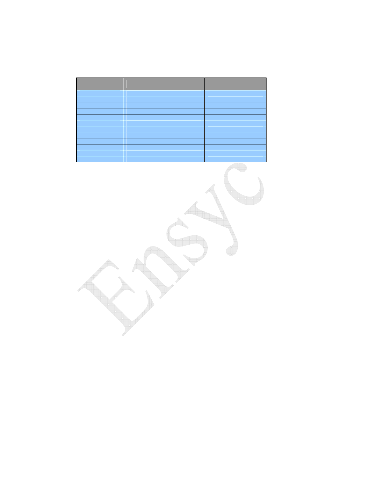
RFID UHF Short Range Controller (RF2400)
__________________________________________________________________________
Note the power level settings are limited by factory minimum and maximum transmit
power configuration.
Power Level Transmit Power (dBm) DC Current (mA)
180 -10.1
190 -4.7
200 -1.0
220 3.9
250 8.3
300 13.1
350 16.5
400 19.1
450 21.2
500 23.0
550 24.6
600 25.8
249
261
271
289
320
384
459
533
618
700
795
872
Table 5-31 Transmit Power Level
Note: average current input to the RF2400 is limited to 550mA for the USB version. A super capacitor is
used to provide more current for a short period of time. Selecting a power level greater then 350 for USB
configurations or 600 for the standard board with the RF Carrier on continuous will exceed power limits
and reset the board. During normal operation capacitance in the power supply meets short term current
requirements
5.2.1.3 Receive Threshold (rxt) command
The Receive Threshold (rxt) command allows the receive threshold to be adjusted for
testing. A decimal parameter represents an A/D count with a scale factor of 0.732 mV
per count. A value of 6 represents 4.4mV at the A/D converter or -68dBm at the antenna
input. This command affects two separate thresholds. The parameter is used directly to
set the signal detect threshold which by default is 15 or 10.98mV or -60dBm at the
antenna input. The receive threshold parameter is scaled by a factor of 5 to set the data
high/low detection levels which by default is 3 or 2.196 mV above or below the average
signal level. The rxt is executed using rxt=n
<CR>
where n is a decimal value from 4 to
64. Upon completion the command prompt is displayed.
5.2.1.4 Phase (phs) command
The Phase (phs) command is used to configure receiver phase of the RF2400. Because
of the controller architecture, signal nulls exist based carrier frequency and tag to antenna
spacing. Selecting the opposite phase will move this null, allowing this tag to be read.
By default, automatic phase control is selected. In the retry scheme, if an error is
encountered in selecting a tag, the opposite phase is tried first before stepping the Tx
power or hopping. If a successful read is accomplished following the phase switch, this
phase setting is saved on a per-channel basis. On commands that have a “Find Tag
Retries”, this must be set to at least one. However, the phase retries are not counted
toward the command’s retry count.
The phs command is executed by typing phs =n
<CR>
where n is a decimal setting. A
value for n equal to 0 or 1 forces either of the two phases while a 2 toggles to the
opposite phase. Any of these three settings disables auto phase switching and are used
________________________________________________________________________
Ensyc
- C
Technologies P
ONFIDENTIAL
AGE
38 11:56:13 AM
- M
ARCH
30, 2008
Page 48

RFID UHF Short Range Controller (RF2400)
__________________________________________________________________________
mainly for debug. Uning n equal to 10 sets auto phase switching on retries and is the
default. Using N equal to 20 initializes the phase per channel table to all 0’s while n
equal to 21 initializes the phase per channel table to all 1’s. Executing the eedef
command initializes the phase per channel table to all 0’s (as well as setting all of the
EEPROM variables to factory defaults). Both the phase setting and phase table are
stored in EEPROM and restored on power-up. By starting with the phase that last
resulted in a good read for a channel, many retries will be eliminated, providing the tag
distance is constant. Upon completion the command prompt is displayed.
5.2.1.5 Tag Class (tc) command
The tag class (tc) command is used to configure the reader for either a Class 1 tags, Gen 2
tags or optionally to automatically identify the tag class. When auto is selected the reader
attempts to initially read a Gen2 class tag and after the retry scheme has been exhausted
will attempt to read a Class 1 tag. This option will extend the time to read a tag and
should be used with an understanding of this limitation. The current tag class can be read
using the
tc
<CR>
command or set using
tc=n
<CR>
, where n is a number from 0x1 to 0x3.
The value 0x1 indicates Class 1, a 0x2 represents Gen2 and a 0x3 represents Auto class.
Upon completion the command prompt is displayed.
5.2.1.6 Read Retry (rrty) command
The read retry (rrty) command is used to establish the number of retries used for either
the Get ID or Get Raw ID host commands. A retry consists of a read attempt at the next
power level defined by the transmit power step command (refer to 5.2.1.2). Every fourth
retry includes a hop to a channel at least 8 channels away and lowers to power level back
to the level defined by the txp0
<CR>
command. The value is persistent and is maintained
when the board is power cycled. The default value is 4. The rrty command is executed
using rrty=nnn
<CR>
where nnn is a value from 0-255 decimal representing the number of
retries. Upon completion the command prompt is displayed.
5.2.1.7 Read Tag
(rt)
command
The read tag (rt) command is used to initiate a single tag read attempt at the current txp
power level without retries. Each execution of the rt command first selects a different
random channel from the configured frequency table, then attempts to read the tag. If
hopping has been disabled (Protected Command) the rt command will not select a new
channel and will always use the same channel. The rt command is executed using
rt
<CR>
. Results of a successful read attempt for a Class 1 or GEN2 tag are displayed on
the command line as fourteen bytes of tag data: (
(
64 or 96
), the CRC (
CRC nnnn
) and channel number (Chnn) . Unsuccessful read attempts
12-bytes EPC)
followed by the ID length
result with an error code detailing the nature of the read failure as shown in Table 5-37.
Upon completion, the command prompt is displayed.
5.2.1.8 Read Loop (rl) command
The read loop (rl) command is used to initiate an iterative rt command. Each iteration of
the rt command operates at a different random channel, from the configured frequency
________________________________________________________________________
Ensyc
- C
Technologies P
ONFIDENTIAL
AGE
39 11:56:13 AM
- M
ARCH
30, 2008
Page 49

RFID UHF Short Range Controller (RF2400)
__________________________________________________________________________
table. If hopping has been disabled (Protected Command) all tag reads will use the same
channel. The rl command is executed using rl
second or rl=nn
<CR>
where nn represents the loop time interval in 10
<CR>
using a default loop interval of ½
ths
of a second.
Results of a successful read attempt for a Class 1 or GEN2 tag are displayed on the
command line as fourteen bytes of tag data: (
or 96
), the CRC (
CRC nnnn
) and channel number (Chnn).
12-bytes EPC)
followed by the ID length (
Unsuccessful read attempts
64
result with an error code detailing the nature of the read failure as shown in Table 5-37.
Entering a
<CR>
will terminate the command. Upon completion, the command prompt is
displayed.
5.2.1.9 Sequential Loop (sl) command
The read loop (sl) command is used to initiate an iterative rt command. Each iteration of
the rt command operates at the next sequential channel, from the configured frequency
table. If hopping has been disabled (Protected Command) all tag reads will use the same
channel. The sl command is executed using sl
second or sl=nn
<CR>
where nn represents the loop time interval in 10
<CR>
using a default loop interval of ½
ths
of a second.
Results of a successful read attempt for a Class 1 or GEN2 tag are displayed on the
command line as fourteen bytes of tag data: (
or 96
), the CRC (
CRC nnnn
) and channel number (Chnn).
12-bytes EPC)
followed by the ID length (
Unsuccessful read attempts
64
result with an error code detailing the nature of the read failure as shown in Table 5-37.
Entering a
<CR>
will terminate the command. Upon completion, the command prompt is
displayed.
5.2.1.10 Write Tag (wt) command
The write tag (wt) command is used to initiate a single tag write attempt at txp0 level
(plus 50) without retries. Hopping is not used for a write operation thus wt commands
will use the same channel. The wt command is executed using wt
<CR>
to write the
default tag ID of 0123456789ABCDEF01234567 or to write a specific tag ID using
wt=nnnnnnnnnnnnnnnnnnnnnnnn
<CR>
where n is one of 24 hex characters
representing the tag EPC code (missing characters are zero filled). For Class 1 tags the
CRC is calculated and appended to the data prior to being written to the tag. For Gen2
tags CRC operations are handled by the Tag. Using Class 1 tags there is no error
checking for the write command and the tag must be read after being written to verify the
operation was completed successfully. Gen2 tags provide a response to a write operation
indicating success or failure. Upon completion, the command prompt is displayed.
5.2.1.11 Lock Tag (lt) command
The lock tag (lt) command is used to establish the kill code and lock the tag to prevent
further modification of the tag ID, or CRC. The lt command will only operate on tags
written in 96 bit format. The lt command is executed using lt=nn
lt=nnnnnnnn
<CR>
where nn is the hexadecimal representation of the kill code for Class1
<CR> or
tags and nnnnnnnn is a hexadecimal representation (must be non-zero) of the kill
password for Gen2 tags. Class 1 tags provide no response to this command while Gen2
________________________________________________________________________
Ensyc
- C
Technologies P
ONFIDENTIAL
AGE
40 11:56:13 AM
- M
ARCH
30, 2008
Page 50

RFID UHF Short Range Controller (RF2400)
__________________________________________________________________________
tags respond with a success or failure status which is provided in the host response. To
verify the tag was properly locked the tag should be read to confirm the read response
consists of only the CRC followed by the 12 bytes of Tag ID data. Upon completion, the
command prompt is displayed.
5.2.1.12 Lock Tag G2 (l2) command
The lock tag G2 (l2) command is specifically used with Gen 2 tags. It allows locking of
individual passwords and memory banks. The lock status for a password or memory bank
can be Perma-locked (making it permanently unchangeable). The command requires 8
bytes of parameters (16 hex character), 4 byte Access Password, 2 byte Mask and 2 byte
Action field. l2=xxxxxxxxyyyyzzzz The Access Password supplied must match that of
the tag’s otherwise the command will fail with a NOTAG response. If an Access
Password has not been written to the tag, it defaults to 00000000.
Refer to the host LOCKG2 command section 5.1.3.11 for further information.
5.2.1.13 Access (apw)
The Access (apw) command allows entry of an Access password for communication with
GEN 2 Tags. This command does not communicate with the tag.
If the tag’s access password is zero, the tag never enters the OPEN state, but goes directly
to the SECURED state and this command is not needed.
If the tag’s access password is non-zero, the tag enters the OPEN state. The password
entered with this command is used with tag reads and writes to bring the tag to the
SECURED state, allowing writes to an area that is non-perma-locked.
5.2.1.14 Kill Tag (kt) command
The kill tag (kt) command permanently erases the tag data or deactivates the tag so it will
no longer respond to or execute reader commands. The kt command attempts to kill the
last tag read eliminating the need to enter a tag ID but requires a kill code that matches
the tag kill code. The command will only operate on tags written in 96 bit format The kt
command is executed using kt=nn
<CR> or
kt=nnnnnnnn
<CR>
where nn is the
hexadecimal representation of the kill code for Class1 tags and nnnnnnnn is a
hexadecimal representation (must be non-zero) of the kill password for Gen2 tags. Class
1 tags provide no response to this command while Gen2 tags respond with a success or
failure status which is provided in the host response. To verify the tag was properly
killed the tag should be read to confirm the read response consists of all zeros or the tag
will no longer responds to reader commands. Upon completion, the command prompt is
displayed.
5.2.1.15 Quiet Tag (qt) command
The quiet tag (qt) command can be used to temporarily prevent a Class 1 tag from
responding to tag commands. The tag enters the sleep state where it no longer responds
________________________________________________________________________
Ensyc
- C
Technologies P
ONFIDENTIAL
AGE
41 11:56:13 AM
- M
ARCH
30, 2008
Page 51

RFID UHF Short Range Controller (RF2400)
__________________________________________________________________________
reader commands except the talk command or the persistence mode limit times out.
Before using this command a read tag rt must be executed to capture the tag ID. The qt
is executed by qt
<CR>.
Upon completion, the command prompt is displayed.
5.2.1.16 Erase Tag (et) command
The erase tag (et) command is used to erase tag data. If the tag is not locked, the IDdata
is erased to zeros for both Class 1 and Gen2 tags. Additionally, the CRC, Kill Code, and
Lock bytes are erased to zero in Class 1 tags. Hopping is not used for an erase operation
thus et commands will always use the same channel. The et command is executed using
et
<CR>.
Upon completion, the command prompt is displayed.
5.2.1.17 Paper Sensor Triggered Read (pstr) command
The paper sensor triggered read (pstr) command is used to enable automatic tag reading
based on the state of the optical reflection sensor. Using this command, triggered reading
can be enabled or disabled, set to operate in host or service port mode, based on
reflection or no reflection and set to persist over power cycling. The triggered read state
(pstrs) can be read using pstr
<CR>
command or set using pstr=n
<CR>
where n (pstrs) is a
value from 0x0-0x3F. The bit definitions for pstrs follow:
Bit 0 enables or disables triggered reads where a one (1) indicates triggered read is
enabled and a zero (0) indicates disabled.
Bit 1 indicates which optical state is used to trigger a read where one (1) triggers the
read on a no reflection and a zero (0) triggers the read on reflection. This bit is
ignored when a switch is used in place of the optical sensor(bit 4 is set to a 1)
Bit 2 is reserved and is ignored. (used internally to indicate host vs SP mode)
Bit 3 establishes if the state persists over power cycles where a one (1) indicates the
state persists over a power cycle and a zero (0) indicates that the state does not
persist.
Bit 4 set to one (1) indicates a switch is used instead of the sensor for triggering. When
Bit 5 determines whether the ID data are returned or stored. A zero (0) indicates to
the switch contacts are closed the state is triggered.
return the ID data immediately, while a one (1) causes the data to be stored in
EEPROM for future retrieval. Refer to the “Dump ID Data” command. Bad
reads are not stored in EEPROM.
When enabled using the pstr command, with bit 5 = 0, triggered read tag data are sent as
ASCII in service port mode.
When storing to EEPROM, only good reads are stored. When the EEPROM log is full
(496 records), the pstr function is terminated. An error message is sent to the service port
(error 43).
Note: To use a switch in place of the paper sensor, wire between J3 pins 1 and 2.
5.2.1.18 Paper Sensor (ps) command
________________________________________________________________________
Ensyc
- C
Technologies P
ONFIDENTIAL
AGE
42 11:56:13 AM
- M
ARCH
30, 2008
Page 52

RFID UHF Short Range Controller (RF2400)
__________________________________________________________________________
The paper sensor (ps) command is used to monitor the output of the optical reflection
sensor for debug purposes. Using the ps command, the sensor is polled and A/D readings
are displayed as a decimal number from 0 to 4095. This number is the difference in
output between the sensor LED driven and not. The number is followed by a zero
indicating no reflection or a one to indicate that there is an object in the optical path. The
ps command is executed using ps
<CR>
and continues until a
<CR>
is sent. Upon
completion, the command prompt is displayed.
5.2.1.19 Paper Sensor Threshold (pst) command
The Paper Sensor Threshold (pst) command sets the trigger point for sensing reflection.
This number represents the sensor A/D reading difference between the emitter LED on
and off. A Hysteresis of 200 is used, that is, once reflection is triggered, the value must
drop 200 before reflection status is reset. Valid values are from 250 to 4000. The pst
command is executed using pst=n
<CR>
where n is a decimal value from 250 to 4000.
Use the ps command to monitor and determine the threshold required for a particular
paper and ink. Upon completion, the command prompt is displayed.
5.2.1.20 Auto Read Tag (art) command
The auto read tag (art) command continuously polls for a tag and when a tag is found and
different from the last tag read, the tag data is sent in service port mode to be displayed or
stored in EEPROM. Bit 0 of a parameter byte determines whether the ID data are
returned or stored. The art command is executed using art=n
<CR>
where n represents a
hexadecimal value. A zero indicates to return the ID data immediately, while a one
causes the data to be stored in EEPROM for future retrieval (refer to the Dump ID Data
command section 5.2.1.21).
When storing to EEPROM, only good reads are stored. When the EEPROM log is full
(496 records), the auto read tag function is terminated. An error message is sent to the
service port (error 43).
This command is illegal if pstr mode is enabled and an illegal response will be displayed.
Entering a
<CR>
or any other command will terminate the art command. Upon
completion, the command prompt is displayed.
________________________________________________________________________
Ensyc
- C
Technologies P
ONFIDENTIAL
AGE
43 11:56:13 AM
- M
ARCH
30, 2008
Page 53

RFID UHF Short Range Controller (RF2400)
__________________________________________________________________________
5.2.1.21 Dump ID Data (did) command
This dump id data (did) command returns ID data that has been stored in EEPROM. A
16 bit parameter is required. The upper byte of the parameter indicates how many
records to return and the lower byte is a sub command. An internal pointer can be
optionally initialized to the first record and is used and tracks records. Subsequent
commands can fetch the next group of records. The data dump will stop whenever a
zeroed record is encountered (end of stored data). The EEPROM (8Kx8) can store up to
496 entries. The did command is executed using did=nnmm
<CR>
where nn represents
the number of records and mm represents the subcommand in hexadecimal.
The lower parameter byte contains a sub-command as follows:
1 Reset pointer and dump.
2 Dump from pointer.
3 Get number of records stored.
4 Clear all.
5.2.1.22 Program Flash (pf) command
The program flash (pf) command invokes the serial port boot loader. The loader is used
to download a firmware upgrade and program the new code into flash memory. Until the
upload sequence is initiated by the host, no change is made to flash memory and the
command can be aborted by power cycling the controller. The host software includes
extensive error checking to confirm that the controller firmware is updated correctly.
When the download completes the controller is auto restarted with the new firmware.
The pf command is executed using pf
<CR>.
A response message FLASH is displayed on
the command line. When the operation is complete and the firmware is restarted, the
initial power-up message “RF2400 Ver xx” is displayed
5.2.1.23 Speaker Test (st) command
The speaker test (st) command beeps the speaker continuously using a one second tone
followed by a one second interval. This command is useful to debug the speaker circuit
operation. The st command is executed using st
<CR>
and continues until
<CR>
is
executed. Upon completion, the command prompt is displayed.
________________________________________________________________________
Ensyc
- C
Technologies P
ONFIDENTIAL
AGE
44 11:56:13 AM
- M
ARCH
30, 2008
Page 54

RFID UHF Short Range Controller (RF2400)
__________________________________________________________________________
5.2.1.24 Beep (beep) command
The beep (beep) command is used to establish the operation of the speaker. The speaker
can operate as a function of read activity, based on the optical trigger, or be completely
disabled. The (beep) command is executed using beep=n where n is a bit mapped value
from 0-7. A value of 0 disables the speaker.
bit 0 selects tag activity beep
bit 1 selects the optical trigger beep
bit 2 selects error beep.
The current beep setting can be read using the
beep
<CR>
command. Activity and
triggered read beeps use a frequency of 1500Hz while the error beep uses 750Hz. Upon
completion, the command prompt is displayed.
5.2.1.25 Set EEPROM Defaults (eedef) command
The set EEPROM defaults (eedef) command is used to rewrite the EEPROM to the factor
defaults. The eedef command is executed using eedef<CR>. Whenever the RF2400
firmware is updated it is recommended to execute this command to insure the EEPROM
has the appropriate settings. Upon completion, the command prompt is displayed.
5.2.1.26 Read EEPROM (ree) command
The read EEPROM (ree) command reads and displays eight (8) consecutive locations
from a user provided starting location. The ree command is executed using ree=nnnn
where nnnn represents the hexadecimal starting address from 0x0000 to 0x1FF8. This
command is provided for debug purposes only. Upon completion, the command prompt
is displayed.
5.2.1.27 No initial message (noim) command
The no initial message (noim) command can be used to enable or disable the RF2400
initial power up message. By default, following power-up, the RF2400 sends an
identifying message out the serial port “RF2400 ver n.nn” where n.nn is the firmware
revision. This message may confuse connected RS232 host equipment. The noim
command is executed using noim=n where n is a 1 to disable or a 0 to enable the
message. This setting is preserved in EEPROM. Upon completion, the command prompt
is displayed.
________________________________________________________________________
Ensyc
- C
Technologies P
ONFIDENTIAL
AGE
45 11:56:13 AM
- M
ARCH
30, 2008
Page 55

RFID UHF Short Range Controller (RF2400)
__________________________________________________________________________
5.2.1.28 Diagnostic (di) command
The diagnostic (di) command is used to verify controller functionality in production. The
diagnostics are executed using di
<CR>.
A set of tests are run in order. If any test fails, the
failed test number and an error code are displayed. Upon completion, the command
prompt is displayed.
Diagnostic Test Summary
Test 1: The two I/O ports are tested to insure that they can be individually set
and cleared. If failure, error code 0x80 indicates a problem with port 0, and 0x81
indicates port 1 failed.
Test 2: Test the photo paper sensor circuit. The test fixture connects all 4
leads together. This connects the LED driver to a 75 ohm pull-up resistor and to
the amplifier input. The diagnostic turns the LED driver on and off and checks
the output of the amplifier through the A/D converter. The amplifier output is
checked at less than 0.25V and more than 2.9V. A failure is indicated by error
code 0x83.
Test 3: The VCO (voltage controlled oscillator) is tested. First,
communication between the microcontroller and the VCO is verified. If fail, and
error code of 0x30 is displayed.
The VCO is tested to insure that the PLL can lock at channels 1, 25, and 48. If
lock is not detected, an error code of 0x31 is displayed.
Test 4: Test the read electronics offset voltage for nominal 1.65V. A failure
with error code of 0x85 indicates that the offset voltage was outside of the range
of 1.4V to 1.8V. Another possible error code that can be encountered here or in
the following test is 0x50 , indicating A/D converter time-out.
Test 5: This test attempts to transmit data while monitoring the receive circuit.
The received signal for this test is caused by a reflection from the tag while
transmitting a modulated signal. The tag is placed at a non-ideal distance from
the antenna to insure some reflection.
The received signal is tested for an average level between 0.5 and 2.5V. This also
insures that the circuitry has not driven to either the ground of 3.3V rail. A failure
here is indicated by error code 0x86.
This test also checks for a P-P (peak-to-peak) signal of at least 0.25V with error
code of 0x87 used to indicate a failure.
Test 6: The final test attempts to read the tag. If successful, the tag ID and
CRC are displayed, followed by the word passed. Possible error codes are 0x20
no tag, or 0x21 tag lost.
________________________________________________________________________
Ensyc
- C
Technologies P
ONFIDENTIAL
AGE
46 11:56:13 AM
- M
ARCH
30, 2008
Page 56

RFID UHF Short Range Controller (RF2400)
__________________________________________________________________________
Diagnostic Error Code Summary
0x20 No Tag detected (read tag fail)
0x21 Tag Lost (read tag fail)
0x30 Chipcon VCO communication fail
0x31 VCO PLL won’t lock.
0x50 A/D converter time-out
0x80 Port 0 fail
0x81 Port 1 fail
0x82 Paper Sensor circuit fail
0x85 Read Offset out-of-range
0x86 Read Average signal out-of-range
0x86 Read signal P-P voltage too low
Additional diagnostic information can be displayed to assist in the diagnosis of problems.
The diagnostic display can be executed using di=d
<CR>
displaying A/D results from the
diagnostics.
ofs=2379 174
min=1935 141
max=2901 212
P-P=966 70
dtxp=250
For the 1st 4 lines, the 1st number following the equal sign is the measured A/D
count and the second number is the reading converted to voltage in hundredths of
a volt. Dtxp is a relative Tx power level which defaults to 250.
The acceptable ranges are:
ofs 1912-2459 (1.4-1.8V)
aver 683-3415(1.5-2.5V)
P-P greater than 966(0.25V)
________________________________________________________________________
Ensyc
- C
Technologies P
ONFIDENTIAL
AGE
47 11:56:13 AM
- M
ARCH
30, 2008
Page 57

RFID UHF Short Range Controller (RF2400)
__________________________________________________________________________
5.2.1.29 Ignore CRC (icrc) command
The ignore CRC (icrc) command is used for debug and testing. This command disables
CRC checking of host commands and eliminates the need to manually calculate the CRC
when using a generic serial port program for communication in host mode. The icrc
command is executed using icrc<CR>. Upon completion, the command prompt is
displayed.
5.2.1.30 Exit (exit) command
The exit (exit) command is used to exit service port mode and resume the media
independent binary command protocol. The exit command is executed using exit
<CR>.
5.2.1.31 Display menu (??) command
The display menu (??) command is used to display the standard service port commands
for reference. The ?? command is executed using ??
<CR>.
Upon completion, the
command prompt is displayed.
________________________________________________________________________
Ensyc
- C
Technologies P
ONFIDENTIAL
AGE
48 11:56:13 AM
- M
ARCH
30, 2008
Page 58

RFID UHF Short Range Controller (RF2400)
__________________________________________________________________________
5.2.1.32 Standard command summary
The following table summarizes the standard service port commands.
Command Type Persistent Range Default Description
baud r/w Yes 0-4 1 Read or set baud rate (see Table 5-6)
txp0 r/w Yes 0-999 215 Tx power step (limit between min-max)
txp1 r/w Yes 0-999 275 Tx power step (limit between min-max)
txp2 r/w Yes 0-999 335 Tx power step (limit between min-max)
txp3 r/w Yes 0-999 400 Tx power step (limit between min-max)
rxt r/w Yes 0-255 15 = (11mV) Read threshold x 0.732mV
phs r/w Yes 0x20 0x10 0, 1, 2=tgl, 0x10=auto, 0x20=init
tc r/w Yes 1-3 2 Tag Class (1=Class1, 2=Gen2, 3= Auto)
rrty r/w Yes 0-255 7 Get ID & Get Raw ID retries
rt e No na na Read tag ID
rl ep No 0-255 5 Read loop (Random) (delay in 1/10 sec)
sl ep No 0-255 5 Sequential loop (delay in 1/10 sec)
wt ep No
lt e No 0x00-0xFF 0x00 Lock Tag
l2 e No 8 bytes na Lock Tag GEN 2
kt e No 0x00-0xFF 0x00 Kill Tag
qt e No Na na Quiet Class 1Tag, must rt first to get ID
et e No na na Erase tag
pstr r/w Programmable 0x0-0x1F na Paper Sensor Triggered Read
ps e No na na Paper sensor displays A/D and 0/1(hit)
pst r/w Yes 250-4000 400 Paper Sensor threshold
art e No flags 0x00 Auto Read Tag (1=store)
did e No Len/sub 0x0000 Dump ID data
pf e No na na Program flash (invokes serial boot mode)
st e No na na Speaker Test
beep r/w Yes 0-2 1
eedef e No na na Set EEPROM to Factory Defaults
ree e No na na Read EEPROM
noim r/w Yes 0/1 0 1 = no initial message at power-up
di ep No d na Diagnostic, =d-display numeric results
icrc w No na off Ignore host cmd CRC (for debug only)
exit e No na na Exit SP mode to host mode
?? e No na na Display menu
24 hex
chars
0123456789ABCDEF01234567
Write tag ID (missing chars are zero filled)
Beep Action (bit map)
bit 0=Activity, bit 1=Trigger, bit2=Error
Table 5-32 Service Port Commands - Standard
________________________________________________________________________
Ensyc
- C
Technologies P
ONFIDENTIAL
AGE
49 11:56:13 AM
- M
ARCH
30, 2008
Page 59

RFID UHF Short Range Controller (RF2400)
__________________________________________________________________________
5.2.2 Protected Commands
The protected commands are for test and setup by qualified service technicians. They
allow setting of parameters for transmit power, channel hopping and frequency selection.
Additionally, the PLL frequency synthesizer internal registers can be accessed. These
settings can affect the legal operation of the unit and are only available to manufacturing
and service personnel. These commands are hidden and only active when the proper
password has been entered using the password command.
5.2.2.1 Password (pw) command
The password (pw) command is used to enable the protected service port commands. The
pw command is entered using pw=n
<CR>
where n is a decimal number from 0 to 65535.
If you require access to the protected commands, contact Ensyc Technologies or your
local service representative for the password. The board may be power cycled to disable
the protected commands or enter an invalid password e.g. pw=0000. Upon completion,
the command prompt is displayed.
5.2.2.2 Transmit power (txp) command
The transmit power (txp) command is used to set or read the output transmit power.
Using txp
from 0 to 600. Using txp=n
<CR>
will display the current transmit power level setting as a decimal number
<CR>
where n is a decimal number from 0 to 600 will set the
current transmit power level. This setting is not limited by the maximum and minimum
transmit power limits. Upon completion, the command prompt is displayed. Power
cycling the board or exiting the SP mode will return the transmit power level to the
default txp[0] setting. Upon completion, the command prompt is displayed.
5.2.2.3 Maximum transmit power (txpmax) command
The maximum transmit power (txpmax) command is used to set or read the maximum
allowed output transmit power. Using txpmax
power level setting as a decimal number from 0 to 600. Using txpmax=n
<CR>
will display the maximum transmit
<CR>
where n is
a decimal number from 0 to 600 will set the maximum transmit power level (refer to
Table 5-31 Transmit Power Level). Additionally any transmit power step setting
greater then the maximum limit will be set to the maximum limit and a message “adjust
steps” is displayed. Upon completion, the command prompt is displayed.
5.2.2.4 Minimum transmit power (txpmin) command
The minimum transmit power (txpmin) command is used to set or read the minimum
allowed output transmit power. Using txpmin
power level setting as a decimal number from 0 to 600. Using txpmin=n
<CR>
will display the minimum transmit
<CR>
where n is
a decimal number from 0 to 600 will set the minimum transmit power level (refer to
Table 5-31 Transmit Power Level). Additionally any transmit power step setting less
then the maximum limit will be set to the minimum limit and a message “adjust steps” is
displayed. Upon completion, the command prompt is displayed.
________________________________________________________________________
Ensyc
- C
Technologies P
ONFIDENTIAL
AGE
50 11:56:13 AM
- M
ARCH
30, 2008
Page 60

RFID UHF Short Range Controller (RF2400)
__________________________________________________________________________
5.2.2.5 Channel select (chan) command
The channel select (chan) command is used to set or read the active channel number.
The chan command chan
number from 0 to 49 and chan=n
<CR>
will display the active transmit channel as a decimal
<CR>
where n is a decimal number from 0 to 49 will set
the active channel. Upon completion the command line returns to the command prompt.
Refer to Table 5-33 for a complete listing of channels and associated frequencies. Upon
completion, the command prompt is displayed.
selects the next random channel prior to the reading the tag. To operate on a single channel disable
hopping (refer to section 5.2.2.6). Also hidden channels 50 & 51 (password protected) provide a means to
select 860MHZ and 960MHz respectively for diagnostic purposes.
Channel Frequency (MHz) Channel Frequency (MHz)
0 902.75 25 915.25
1 903.25 26 915.75
2 903.75 27 916.25
3 904.25 28 916.75
4 904.75 29 917.25
5 905.25 30 917.75
6 905.75 31 918.25
7 906.25 32 918.75
8 906.75 33 919.25
9 907.25 34 919.75
10 907.75 35 920.25
11 908.25 36 920.75
12 908.75 37 921.25
13 909.25 38 921.75
14 909.75 39 922.25
15 910.25 40 922.75
16 910.75 41 923.25
17 911.25 42 923.75
18 911.75 43 924.25
19 912.25 44 924.75
20 912.75 45 925.25
21 913.25 46 925.75
22 913.75 47 926.25
23 914.25 48 926.75
24 914.75 49 927.25
Note: with hopping enabled the read command
Table 5-33 RF2400 USA Hopping Table
Channel Frequency (MHz) Channel Frequency (MHz)
Table 5-34 RF2400 E.U. Hopping Table TBD
Channel Frequency (MHz) Channel Frequency (MHz)
Table 5-35 RF2400 Japan Hopping Table TBD
________________________________________________________________________
Ensyc
- C
Technologies P
ONFIDENTIAL
AGE
51 11:56:13 AM
- M
ARCH
30, 2008
Page 61

RFID UHF Short Range Controller (RF2400)
__________________________________________________________________________
5.2.2.6 Hop (hop) command
The hop (hop) command is used to enable or disable frequency hopping. Using the hop
command hop
enabled. The hop command hop=0
<CR>
will display the current hop state where a one indicates hopping is
<CR>
will disable frequency hopping and hop=1
<CR>
will enable frequency hopping. Upon completion, the command prompt is displayed.
5.2.2.7 Gen2 Read (g2r) command
The Gen2 Read (g2r) command allows reading any memory area of the Gen2 tag. A
required 16 bit parameter defines the area to read. Bits 15-12 select the bank, bits 11-8
specify the length in words, bits 7-0 select the word address within the bank (refer to the
Table 5-42 – Memory Map). If any part of the requested area is not supported by the tag,
an error 26 (TAGNXM) is returned. If any part of the area is read-locked, an error 25
(TAGLOCKED) is returned. If the command is successful, the requested data are
displayed. The g2r is executed using g2r=nnnn<CR> where nnnn is the hexadecimal
representation of the 16 bit parameter. For example, g2r=2200 reads the 1st 2 words of
TID memory. This command is only supported for GEN 2 tags. Upon completion, the
command prompt is displayed.
5.2.2.8 Gen2 Write (g2w) command
The Gen2 Write (g2w) command allows up to 8 words to written to any memory area of
the Gen2 tag. The required parameter specifies the data to write in hexadecimal. The
command must be preceded by a g2r command selecting the bank, length and address. If
any part of the requested area is not supported by the tag, an error 26 (TAGNXM) is
returned. If any part of the area is write-locked, an error 25 (TAGLOCKED) is returned.
The g2w is executed using g2w=n…n<CR> where n…n is the hexadecimal
representation of the data to be written from 4 to 32 characters. This command is only
supported for GEN 2 tags. Upon successful completion, the command prompt is
displayed.
5.2.2.9 Transmit zeros (t0) command
The transmit zeros (t0) command is used to enable the transmit carrier and intermittently
modulate the carrier with zeros. The carrier is turned on and modulated with a 50 percent
duty cycle with a modulation period of 1ms. Zeros are transmitted at a frequency of
approximately 70KHz where the carrier is modulated for 1/8 of the cell time. The t0
command is executed using t0
<CR>.
Entering a
<CR>
will terminate the command. Upon
completion, the command prompt is displayed.
________________________________________________________________________
Ensyc
- C
Technologies P
ONFIDENTIAL
AGE
52 11:56:13 AM
- M
ARCH
30, 2008
Page 62

RFID UHF Short Range Controller (RF2400)
__________________________________________________________________________
5.2.2.10 Transmit ones (t1) command
The transmit ones (t1) command is used to enable the transmit carrier and intermittently
modulate the carrier with ones. The carrier is turned on and modulated with a 50 percent
duty cycle with a modulation period of 1ms. Ones are transmitted at a frequency of
approximately 70KHz where the carrier is modulated for 3/8 of the cell time. The t1
command is executed using t1
<CR>.
Entering a
<CR>
will terminate the command. Upon
completion, the command prompt is displayed.
5.2.2.11 Transmit alternating (ta) command
The transmit alternating (ta) command is used to enable the transmit carrier and
intermittently modulate the carrier with alternating ones and zeros. The carrier is turned
on and modulated with a 50 percent duty cycle with a modulation period of 1ms. Ones
are transmitted at a frequency of approximately 70KHz where the carrier is modulated for
3/8 of the cell time. Zeros are transmitted at a frequency of approximately 70KHz where
the carrier is modulated for 1/8 of the cell time. The ta command is executed using
ta
<CR>.
Entering a
<CR>
will terminate the command. Upon completion, the command
prompt is displayed.
5.2.2.12 Transmit random (tr) command
The transmit random (tr) command is used to enable the transmit carrier and
intermittently modulate the carrier with random data. The carrier is turned on and
modulated with a 50 percent duty cycle with a modulation period of 1ms. Data are
transmitted at a frequency of approximately 70KHz where the carrier is modulated for
3/8 of the cell time for a data one and 1/8 of the cell time for a data zero. The tr
command is executed using tr
<CR>.
Entering a
<CR>
will terminate the command. Upon
completion, the command prompt is displayed.
5.2.2.13 Transmit data (td) command
The transmit data (td) command is used to enable the transmit carrier and intermittently
modulate the carrier with the data parameter. The carrier is turned on and modulated
with a 50 percent duty cycle with a modulation period of 1ms. The 16 bit parameter
represents 2 transmitted cell times. The carrier is on for ones, off for zeros. For example,
80E0h sends a zero (modulated 1/8 of the cell time) and a one (modulated 3/8 of the cell
time) The td command is executed using td=nnnn
representation of the 16 bit parameter. Entering a
<CR>
where nnnn is the hexadecimal
<CR>
will terminate the command.
Upon completion, the command prompt is displayed.
________________________________________________________________________
Ensyc
- C
Technologies P
ONFIDENTIAL
AGE
53 11:56:13 AM
- M
ARCH
30, 2008
Page 63

RFID UHF Short Range Controller (RF2400)
__________________________________________________________________________
5.2.2.14 Carrier on (con) command
The transmitter on (con) command is used to turn on the un-modulated transmit carrier.
The con command is executed using con
<CR>.
Upon completion, the command prompt
is displayed.
5.2.2.15 Carrier off (coff) command
The transmitter off (coff) command is used to turn off the transmit carrier. The coff
command is executed using coff
<CR>.
Upon completion, the command prompt is
displayed.
5.2.2.16 Localization (local) command
The localization (local) command is used to configure the controller parameters for
operation under various jurisdictions. Using local
<CR>
will display the current
localization code setting as a decimal number from 1 to ? where 1 = USA, 2 = E.U., and
3 = Japan. Using local=n
<CR>
where n is a decimal number from 1 to ? will set the
localization code.. Upon completion, the command prompt is displayed.
Note currently only the 1= USA Localization is supported
5.2.2.17 Chipcon register read (ccr) command
The Chipcon register read (ccr) command is used to display the contents of the addressed
Chipcon register. The ccr command ccr
AAXX<CR>
, where AA is the hexadecimal
register address and XX is hexadecimal dummy data, will display the contents of the
register on the command line as two hexadecimal digits 0xDD following an equals sign.
Upon completion, the command prompt is displayed.
5.2.2.18 Chipcon register write (ccw) command
The Chipcon register write (ccw) command is used to set the contents of the addressed
Chipcon register. The ccw command ccw
AADD<CR>
, where AA is the hexadecimal
register address and DD is hexadecimal data, will display the contents of the register on
the command line as two hexadecimal digits 0xDD following an equals sign. Upon
completion, the command prompt is displayed.
________________________________________________________________________
Ensyc
- C
Technologies P
ONFIDENTIAL
AGE
54 11:56:13 AM
- M
ARCH
30, 2008
Page 64

RFID UHF Short Range Controller (RF2400)
__________________________________________________________________________
5.2.2.19 Protected command summary
The following table summarizes the protected service port commands
Command Type
pw w No 0-65535 na Password, in decimal
txp r/w No 0-999 215 Tx power in decimal
txpmax r/w Yes 0-999 500 Tx power max limit
txpmin r/w Yes 0-999 180 Tx power min limit
chan r/w No 0-49 30 Frequency (channel) in decimal
hop r/w No 0/1 1=hop Hop flag
g2r ep No 0-FFFFh na Bank(4bits), len (4bits), adr (8bbits)
g2w ep No 0-FFFFh Na Write data word (uses extent from g2r)
t0 e No na na Continuous send 0s (1/8 cell)
t1 e No na na Continuous send 1s (3/8 cell)
ta e No na na Alternating 1s & 0s
tr e No na na Random Data ( pattern for FCC testing)
td ep No 0-FFFFh Na Continuous send parameter
con e No na Carrier on, unmodulated
coff e No na off Carrier disabled
local r/w Yes 1-3 1 Localization code
ccw w No Adr/data Write ChipCon regs (AADD) hex adr/data
ccr w No Adr/data Read ChipCon regs (AAXX) hex adr/don’t care
cci e No na na ChipCon init (as done at power-up)
Persisten
t
Range Default Description
Table 5-36 Service Port Commands - Protected
For r or e types, enter command with <cr> to read or execute. For w types enter command followed by
“=parameter<cr>” to write. For r/w or ep types, enter command with <cr> to read or execute , enter
command followed by “=parameter<cr>” to write or execute with parameters.
________________________________________________________________________
Ensyc
- C
Technologies P
ONFIDENTIAL
AGE
55 11:56:13 AM
- M
ARCH
30, 2008
Page 65

RFID UHF Short Range Controller (RF2400)
__________________________________________________________________________
5.2.3 Service port error codes
Several error codes are presented in service port mode. These include errors that the
firmware identifies when initializing and errors encountered when executing specific
service port commands. These errors are listed in Table 5-37.
Error Code Description
10 Host command invalid
11 Host command CRC error
12 Host command length error
20 No Tag Found – (timeout on sync character)
21 Invalid Tag ID Length – (error during tag read operation)
22 CRC Error –(calculated CRC doesn’t match the tag CRC)
23 Tag response handle mismatch (Gen2 only)
24 Tag returned (Gen2 only)
25 Tag command failed – Tag is locked (Gen2 only)
26 Tag memory address non-existent (Gen2 only)
27 Write verify fail
30 Bad CCRegister Access–(register doesn’t respond or responds with incorrect data)
31 VCO not locked – (The VCO isn’t locked to the requested frequency)
32 No Backscatter – (The receiver didn’t detect any backscatter signal)
40 EEPROM Timeout – (EEPROM bad or missing)
41 EEPROM bad status
42 EEPROM checksum error
43 EEPROM log full
50 ADC timeout
80 Diagnostic Port0 fail
81 Diagnostic Port1 fail
82 Diagnostic read offset out-of-bounds
83 Diagnostic read average out-of-bounds
84 Diagnostic read P-P out-of-bounds
Table 5-37 Service Port Error Codes
________________________________________________________________________
Ensyc
- C
Technologies P
ONFIDENTIAL
AGE
56 11:56:13 AM
- M
ARCH
30, 2008
Page 66

RFID UHF Short Range Controller (RF2400)
__________________________________________________________________________
5.3 RADIO FREQUENCY INTERFACE
The RF2400 controller is designed to communicate with both Auto-ID Class 1 and Class
1 Gen 2 tags operating in the frequency range of 860MHz-960MHz. The controller can
be configured to automatically detect the tag type or fixed to a specific type. The Fixed
configuration has the advantage of accelerating operations eliminating retries to
determine tag type. This dual functionality provides compatibility with existing
technology while providing support for next generation tags. The radio frequency (RF)
interface and Reader protocol are based on a reader “talks” first passive RFID system
using half-duplex communication.
5.3.1 Auto-ID Class 1
The RF2400 reader incorporates an Auto-ID Class 1 RF communication interface and
Reader functionality. Data symbols communicated between the reader and the tag
include a binary zero (0), a binary one (1), a null, and punctuation. The encoding and
modulation of these symbols and protocols follow the MIT Auto-ID Center – Technical
Report - 860MHz–930MHz Class 1 Radio Frequency Identification Tag Radio
Frequency & Logical Communication Interface Specification Candidate
Recommendation, Version 1.0.1 – November 14, 2002
The RF2400 reader initiates all communications with the Class 1 tags which occur in a
half-duplex manner. Class 1 tags communicate using backscatter modulation. This
communication only occurs when directed by a properly decoded and interpreted
command emitted from a Reader.
5.3.1.1 Class 1 Reader-Tag RF communications
The RF2400 communicates with the Class 1 tags using amplitude shift keying (ASK).
The modulation operates at 90% nominally. Shaped Keying is employed to control
modulation rise and fall times in order to more rapidly roll off sideband energy.
Modulation parameters for North American operation are summarized in Table 5-38
Parameter Description Value
To Master Clock Interval 14.25 us
Totol Master Clock Interval Tolerance <0.1%
1/T0 Data Rate 70.18 Kbps
Tfwhmo Half Width Binary 0 (1/8 T0) 1.78 us
Tfwhm1 Half Width Binary 1 (3/8 T0) 5.34 us
Mod Modulation Depth 90%
DMod Modulation Depth Variation 5%
Tf Fall Time 300 ns typ.
Tr Rise Time 300 ns typ.
Ripple Ripple <10%
Table 5-38 Class 1 Reader-Tag Modulation Parameters
________________________________________________________________________
Ensyc
- C
Technologies P
ONFIDENTIAL
AGE
57 11:56:13 AM
- M
ARCH
30, 2008
Page 67

RFID UHF Short Range Controller (RF2400)
__________________________________________________________________________
The Reader data modulation incorporates a pulse width scheme to represent logical bits 0
and logical bits 1. A logical 0 is represented by a cell time of 1/8 T0 (see Figure 5-5).A
logical 1 is represented by a cell time of 3/8 T0 (see Figure 5-5).
Figure 5-5 Class 1 Reader Modulation Timing for Binary 0
A logical 1 is represented by a cell time of 3/8 T0 (see Figure 5-6).
Figure 5-6 Class 1 Reader Modulation Timing for Binary 1
5.3.1.2 Class 1 Tag-Reader RF communications
The Tag communicates to the Reader by backscatter modulation of the continuous wave
(CW) carrier supplied by the Reader. This is an ASK modulation and is typically 10% or
less of the signal amplitude based on nominal radiation cross-sections. The Tag to
Reader bit cell time is ½ T0 resulting in a nominal data rate twice the data rate from the
Reader to the Tag. However, this rate will vary over the response as much as 25% as the
Tag power level changes. Tag the Reader parameters for North America are summarized
in Table 5-39.
Parameter Description Value
To Master Clock Interval 14.25 us
Ttagbitcell Tag to Reader Bit Cell Interval T0/2 7.13 us
Tag Data Rate Tag to Reader Nominal Data Rate 2/T0 140.35 Kbps
Table 5-39 Class 1 Tag-Reader Communication Parameters
________________________________________________________________________
Ensyc
- C
Technologies P
ONFIDENTIAL
AGE
58 11:56:13 AM
- M
ARCH
30, 2008
Page 68

RFID UHF Short Range Controller (RF2400)
__________________________________________________________________________
Tag modulation uses a four interval bit cell encoding technique. Two transitions
represent a binary 0 and four transitions represent a binary 1 (see Figure 5-7).
Figure 5-7 Class 1 Tag to Reader Encoding
5.3.2 Class 1 – Gen 2
The RF2400 incorporates a Class1 Gen 2 RF communication interface compatible with
the new generation of GEN 2 tags. Gen 2 support is much more robust then Class 1 tags
providing enhanced features and improvements with security and the mechanisms to
handle large populations of tags. Encoding, modulation and protocols follow the EPC™
Radio-Frequency Identity Protocols Class-1 Generation-2 UHF RFID Protocol for
Communications at 860 MHz – 930 MHz Version 1.0.9 – January 31, 2005
5.3.2.1 Gen 2 Reader-Tag RF communications
The RF2400 communicates with the Gen 2 tags using amplitude shift keying (ASK).
Modulation operates at 90% nominally and shaped Keying is employed to control
modulation rise and fall times. Communications between the Reader and Tags is based
on a reference time interval defined as a Tari which is the duration of a data 0. Fixed
format is used for all communications. Modulation parameters for North American
operation are summarized in Table 5-40
________________________________________________________________________
Ensyc
- C
Technologies P
ONFIDENTIAL
AGE
59 11:56:13 AM
- M
ARCH
30, 2008
Page 69

RFID UHF Short Range Controller (RF2400)
__________________________________________________________________________
Parameter Description Value
Tari Reference Time Interval 12.5 us
Ttol Reference Interval Tolerance <0.1%
1/(2Tari) Data Rate 40 Kbps
PW RF Pulse Width (Tari/2) 3.125 us
Mod Modulation Depth 90%
DMod Modulation Depth Variation 5%
Tf Fall Time 300 ns typ.
Tr Rise Time 300 ns typ.
Ripple Ripple <10%
Table 5-40 Gen 2 Reader-Tag Modulation Parameters
Data is transmitted using Pulse Interval Modulation PIE encoding. A fixed pulse width
of ½ Tari is used for both logic 0 and logic 1 data bits. A data zero is represented by
positioning this pulse at the last half of the first Tari interval. A data 1 is represented by
positioning the pulse at the last half of the second Tari interval (refer to Figure 5-8).
Figure 5-8 Gen 2 Reader to Tag PIE Encoding
5.3.2.2 Gen 2 Tag-Reader RF communications
The Tag communicates to the Reader by backscatter modulation of the continuous wave
(CW) carrier supplied by the Reader. This is an ASK modulation and is typically 10% or
less of the signal amplitude based on nominal radiation cross-sections. The Tag to
Reader bit cell time is ½ Tari resulting in a nominal data rate twice the data rate from the
Reader to the Tag. However, this rate will vary over the response as much as 25% as the
Tag power level changes. Tag the Reader parameters for North America are summarized
in Table 5-41
________________________________________________________________________
Ensyc
- C
Technologies P
ONFIDENTIAL
AGE
60 11:56:13 AM
- M
ARCH
30, 2008
Page 70

RFID UHF Short Range Controller (RF2400)
__________________________________________________________________________
Parameter Description Value
Tari Master Clock Interval 8 us
Tag Data Rate Tag to Reader Nominal Data Rate 1/Tari 125 Kbps
Table 5-41 Gen 2Tag-Reader Communication Parameters
The Reader determines the TAG encoding scheme and data rate with a Query command.
The RF2400 always selects FM0 encoding. Using FM0 a binary 0 is represented by a
transition mid bit cell and a binary 1 is represented by no transitions within the cell (refer
to Figure 5-9)
Figure 5-9 Gen2 Tag to Reader Encoding
________________________________________________________________________
Ensyc
- C
Technologies P
ONFIDENTIAL
AGE
61 11:56:13 AM
- M
ARCH
30, 2008
Page 71

RFID UHF Short Range Controller (RF2400)
__________________________________________________________________________
5.4 LOGICAL STRUCTURES AND DATA CONTENT
5.4.1 Gen 2 Tag Structures and Data content
The Gen 2 tag memory is logically separated into four banks. Each bank may contain
zero or more memory words. The memory map follows.
Bank Area
11 User
10 TID
01 EPC
00 Reserved
MSB
xxh User [15:0]
00h User [N:N-15] 0Fh
. . .
10h TID [15:0] 1Fh
00h TID [31:16] 0Fh
xxh EPC [15:0]
. . .
20h EPC [N:N-15] 2Fh
10h PC [15:0] 1Fh
00h CRC-16 [15:0] 0Fh
. . .
30h Access Password [15:0] 3Fh
20h Access Password [31:16] 2Fh
10h Kill Password [15:0] 1Fh
00h Kill Password [31:16] 0Fh
Content
. . .
LSB
Table 5-42 Class 1 Gen 2 Memory Map
User Memory is for user specific data storage. This region is Tag vendor specific.
TID memory contains an 8 bit allocation class identifier, and information to describe any
custom capabilities of the Tag. The TID may include a Tag mask-designer identified,
Tag model number, Tag serial number, etc
EPC memory contains a CRC16 to protect the EPC, a Protocol Control (PC) field to
describe the length of the EPC, and the EPC (Electronic Product Code). The RF2400
currently supports an EPC of 12 bytes.
Reserved memory contains the kill and access passwords. The default (unprogrammed) value of the both passwords is zero. An Interrogator can use the kill
password once to kill a Tag and render it silent thereafter. The access password, if nonzero shall require the interrogator to issue this Password before transitioning to the
secured state.
.
________________________________________________________________________
Ensyc
- C
Technologies P
ONFIDENTIAL
AGE
62 11:56:13 AM
- M
ARCH
30, 2008
Page 72

RFID UHF Short Range Controller (RF2400)
__________________________________________________________________________
5.5 AUTONOMOUS OPERATION
The RF2400 includes functionality to support remote autonomous operation. The
controller is easily configured to read tags remotely (disconnected from the host
communication port) saving tag ID data to EEPROM while operating under battery
power. Functions supported include:
Paper Sensor Triggered Read (Host mode). Refer to section 5.1.2.7.1
Paper Sensor Triggered Read (Service Port mode). Refer to section 5.2.1.17
Auto Get Tag ID (Host mode). Refer to section 5.1.3.3
Auto Read Tag (Service Port mode). Refer to section 5.2.1.20
The onboard EEPROM log is sized to store up to 496 ID records. Each record stores the
complete EPC ID (up to 96 bits), the tag CRC, the length of the EPC, as well as the
function used to store the ID. Once the log is full (all 496 locations written), the
operational function will be terminated and a message is immediately sent to the host
communication port; however, if the communication port is disconnected at that time the
message will be lost. When connected to the communication port, the host can
interrogate the reader using the “Get Reader Status” command (refer to section 5.1.2.5)
with the data byte set to 0x00. If the log is full, the response will return a message type
of 0x98 (log full). The host can download the stored ID data and clear the log using the
“Dump ID Data” command (refer to section 5.1.3.4).
If operating in service port mode, when the host connection is established using the
“^P^D” protocol, and the log is full, a message “Error 43” will be sent. The ID data can
be retrieved and the log cleared using the did command (refer to section 5.2.1.21).
________________________________________________________________________
Ensyc
- C
Technologies P
ONFIDENTIAL
AGE
63 11:56:13 AM
- M
ARCH
30, 2008
Page 73

Page 74

RFID UHF Short Range Controller (RF2400)
__________________________________________________________________________
6 HARDWARE DESCRIPTION
The RFID controller (RF2400) is interfaced to a host processor with an industry standard
RS232 interface (or optional USB adapter) using a media independent protocol. The
reader is designed around a Texas Instrument TMS320F2808 low cost DSP used to
communicate with the host and control all RFID transmit and receive operations. The
DSP provides a wide selection of memory including 128 Kbytes of Flash, 2 Kbytes of
OTP ROM, 8 Kbytes of Boot ROM Peripherals include up to four Hardware PWM
outputs, six 32-bit timers, six 16-bit timers, four SPI modules, two SCI communication
ports, two eCAN modules, sixteen channels of 12-ADC, and 35 individually
programmable GPIO pins. To limit cost, the majority of the RFID reader functionality is
implemented in the DSP firmware. Combined with a 128-Bit security Key/Lock this
provides a mechanism to deter theft of the RFID intellectual property (IP).
A low cost highly integrated VCO, operating over the frequency range 860MHz960MHz, is used to create the RF carrier signal and under DSP control provides the
frequency hopping spread spectrum (FHSS) mechanism in accordance with FCC part
15.247. A power splitter divides the VCO output into the RF carrier and a local reference
signal used to demodulate the RFID backscatter signal. A single chip 2-watt GSM Power
Amplifier boosts the RF carrier necessary for reliable communication and is adjustable
from 0dBm (1mW) to 24dBm (250mW). The amplifier output is coupled to the antenna
with an integral directional coupler to reduce the transmitter signal coupled to the
receiver section.
The output of the directional coupler applies the backscatter signal directly to an RF
mixer. Using the local reference signal from the power splitter, a selectable LC phase
delay is used to directly convert the in-phase or quadrature components of backscatter
signal from the RFID tag to baseband. A low-pass RF filter removes any high frequency
products of the mixer. This filter output is applied to a high-pass network coupled with a
synchronized FET switch to remove any DC components. Finally a base-band amplifier
boosts the signal to a level compatible with the DSP analog input. The processor phase
locks to the signal, synchronizes to the clock edges, tracks the average signal level, and
decodes the data stream for presentation to the host.
________________________________________________________________________
Ensyc
- C
Technologies P
ONFIDENTIAL
AGE
65 11:56:13 AM
- M
ARCH
30, 2008
Page 75
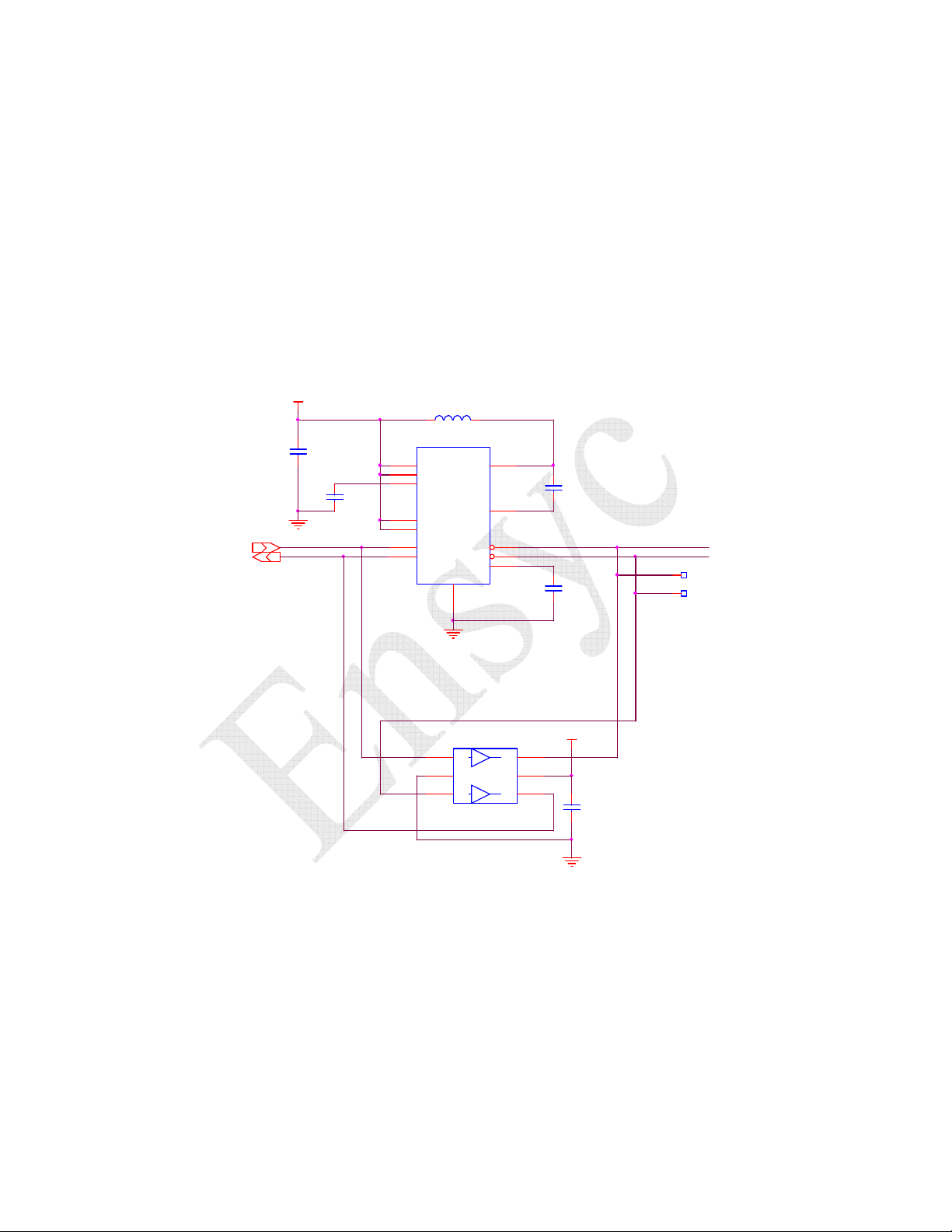
RFID UHF Short Range Controller (RF2400)
__________________________________________________________________________
6.1 HOST COMMUNICATION INTERFACE
The RF2400 reader is interfaced to the host using an industry standard RS232 or optional
TTL serial interface. Populating the controller with
the DSP media independent serial protocol to industry standard RS232 signal levels.
Optionally, removing the RS232 components and populating components
provides a TTL compatible signal level. The serial interface offers no hardware or
software flow control and only communicates using the serial transmit and receive data
lines. Baud rate defaults to 19,200 k-baud using eight data bits and one stop bit. The
baud rate can be reconfigured using host commands.
U14 L10,
and
C63, C64,C67, C69
interfaces
U15
and
C71
+3V3
C69
1uF
10V
1
D
RSTXD3
RSRXD3
RS232 Serial Interface
C67
1uF
10V
L10 10uH
U14
3
VCC
10
VL
4
VDD
1
8
PS
9
MODE
11
TIN
12
ROUT
1
SW
CAP
TOUT
RIN
VEE/PAD
GND
LTC2801CDE
6
D
5
7
2
1
13
1
C64
220nF
16V
1
C63
1uF
10V
1
HSERTX
HSERRX
TN526
TN525
TTL Serial Interface
+3V3
6
5
4
C71
100nF
2,3
1
1A
2
GND
3
2A
U15
74LVC2G17
2,3
1Y
VCC
2Y
D
Figure 6-1 Host Interface
________________________________________________________________________
Ensyc
- C
Technologies P
ONFIDENTIAL
AGE
66 11:56:13 AM
- M
ARCH
30, 2008
Page 76

RFID UHF Short Range Controller (RF2400)
__________________________________________________________________________
6.2 DSP PROCESSOR
The heart of the RF controller is a 100 MIPS DSP processor. The processor includes a
crystal oscillator which runs at 20MHz, set by an external crystal. An integral PLL
boosts the frequency to 100MHz. During tag communication, the processor must run at
100MHz to achieve the timing required. When not communicating with a tag, firmware
decreases the operating frequency to 20MHz to conserve power. As the operating
frequency is changed, internal dividers, timers, and the baud rate generator are adjusted
to maintain correct operation.
The processor has hardware for serial communication including UART, I2C, and SPI.
The UART is used for host communication through an external RS232 translator or
buffered TTL interface. The I2C controller interfaces to an external EEPROM. Two SPI
interfaces are implemented, one communicates with the Chipcon VCO, the other is used
to serialize the transmitted data, it’s clocking is supplied by an integral PWM.
An integrated 12 bit A/D converter samples the tag received data after pre-conditioning.
The processor firmware then decodes the data while tracking frequency and amplitude
variations. The A/D also monitors board voltage levels to insure proper operation and to
control charging of an optional battery.
Several PWMs are used for transmit power level setting, beeper sound generation, and
transmit data gating.
General purpose I/O ports control various transmit and receive functions, LED indicators,
and 2 software controlled external I/O ports.
6.3 EEPROM
An EEPROM memory is used to permanently store required settings and tag ID data.
The EEPROM interfaces with the processor over an I2C bus. Parameters stored include
such items a Tx power, Rx thresholds, host comm. settings, etc. A large area is used to
store tag IDs for portable data gathering while not connected to a host computer.
The EEPROM currently used is 64kbits or 8Kx8. Following is the EEPROM map:
0-1F parameters
40-77 phase table, entry per channel
78-79 store pointer for ID storage
80-9F demo data
100-1FFF ID storage 16 bytes each for 496 entries
________________________________________________________________________
Ensyc
- C
Technologies P
ONFIDENTIAL
AGE
67 11:56:13 AM
- M
ARCH
30, 2008
Page 77

RFID UHF Short Range Controller (RF2400)
__________________________________________________________________________
6.4 TRANSMITTER/VCO
The Transmitter/VCO is implemented using a Chipcon CC1070 Single Chip Low Power
RF Transmitter. This component interfaces to the processor using an SPI interface and
incorporates the necessary circuitry to implement Frequency Hopping Spread Spectrum
(FHSS) signaling for noisy environments and to meet agency spectral requirements. To
enhance speed of operation, the Transmitter/VCO includes dual sets of frequency control
registers to allow overlapped frequency configuration during operation. UHF frequency
is synthesized from an inexpensive 14.7456MHz crystal using a programmable fractional
divider to achieve high resolution which is ideal for narrow band applications. An
external loop filter is provided to meet the stabilization requirements imposed by FHSS.
The VCO circuitry with associated filtering can be configured to operate over the range
from 850MHZ to 960MHz. Although the CC1070 provides modulation control, for
purposes of flexibility and to provide more control of various modulation schemes these
features are not used. The output power of the VCO is adjustable from -30dBm to
+7dBm. The output is coupled through an impedance matching which attenuates
harmonic components and matches the combined power amplifier and mixer circuitry
impedance to maximize VCO output power.
6.5 POWER SPLITTER
The power splitter is asymmetric dividing the power from the VCO to the RF amplifier
and mixer. The mixer requires ample signal to reduce conversion loss as compared to the
minimal input requirements of the RF amplifier. The circuit is implemented using an
inductor and two capacitors.
6.6 POWER AMPLIFIER
The RF power amplifier is based on the Triquint TQM7M4006 Quad Band Power
Amplifier Module. This device is a low cost amplifier designed for the cellular phone
market providing and efficient low cost solution. The amplifier is controlled using a
voltage controlled input to both set the output power and provide a versatile means to
amplitude modulate the carrier.
6.7 PA MODULATION
The Processor directly modulates the carrier with ASK modulation using the voltage
controlled input of the RF Power Amplifier. A processor PWM output is filtered using a
2-pole Sallen-Key low pass filter providing the required control voltage. This voltage is
configurable and establishes the output power of the RF2400. Using two low resistance
analog SPST switches the power amplifier control voltage input is switched between zero
and this reference voltage using shaped key drive to more rapidly roll off sideband
energy.
________________________________________________________________________
Ensyc
- C
Technologies P
ONFIDENTIAL
AGE
68 11:56:13 AM
- M
ARCH
30, 2008
Page 78

RFID UHF Short Range Controller (RF2400)
__________________________________________________________________________
6.8 DIRECTIONAL COUPLER/RF FILTER
The output of the power amplifier is coupled to the antenna using a PCB implemented
directional coupler with 8dB coupling loss and directivity between 25dB and 30dB. This
implementation provides a very low cost alternative while providing the necessary
transmitter/Receiver isolation. The output of the direction coupler is connected to the
antenna using a simple pi filter to further attenuate harmonic components.
6.9 SELECTABLE LC PHASE DELAY/MIXER
The output of the VCO is connected to the mixer using a selectable phase delay with a
nominal 90 degree phase difference. This circuitry also provides additional impedance
matching to provide the strong signal required by the mixer to reduce conversion loss.
The selectable delay provides a unique low cost solution to compensate for receiver nulls
related to frequency and the tag to antenna spacing. Using a passive mixer the received
signal is converter directly to baseband.
6.10 BASE-BAND AMPLIFIER
The output of the mixer is coupled with an impedance matching circuit to an acquisition
switched high-pass filter to remove the large DC component. The output of this filter is
applied to the 34dB base-band amplifier which incorporates 800 KHz low-pass filter
limiting the bandwidth of the amplified signal.
________________________________________________________________________
Ensyc
- C
Technologies P
ONFIDENTIAL
AGE
69 11:56:13 AM
- M
ARCH
30, 2008
Page 79
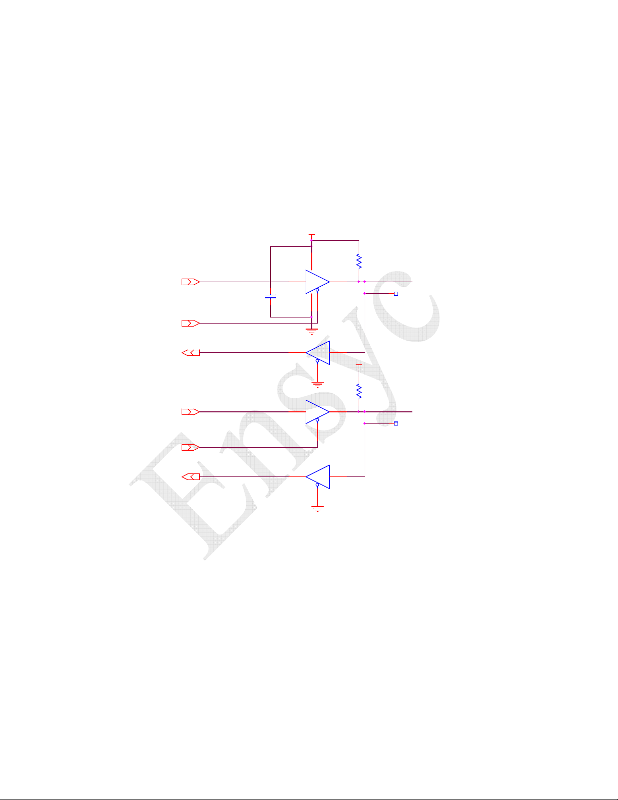
RFID UHF Short Range Controller (RF2400)
__________________________________________________________________________
6.11 GENERAL PURPOSE DIGITAL I/O PORT
The RF2400 provides two bi-directional IO ports which can be independently configured
through software as an input or output port. These ports are buffered and include a
protection circuit allowing an input signal range from 0 to 7volts. A low level is
represented by any input signal less then 0.3V and high level any signal greater then
2.3volts. A 6.8K on-board resistor is provided to pull up the inputs to 3.3volts. An
output low level output voltage is 0.36V at 8mA and a high level output voltage is 2.58V
at -4mA. The IO ports are available on the Digital IO Connector (J2)
+3V3
R513
1,2,3
+3V3
6K8
1,2,3
R514
6K8
1,2,3
PORT0
TN516
PORT1
TN517
U17A
C73
100nF
1,2,3
74VHC125
1,2,3
74VHC125
1,2,3
2 3
1147
D
U17B
6
4
D
U17C
9 8
74VHC125
10
U17D
13
D
74VHC125
5
1,2,3
1211
PORTO03
PORTEN#03
PORTI03
PORTO13
PORTEN#13
PORTI13
Figure 6-2 Digital I/O Port
________________________________________________________________________
Ensyc
- C
Technologies P
ONFIDENTIAL
AGE
70 11:56:13 AM
- M
ARCH
30, 2008
Page 80

RFID UHF Short Range Controller (RF2400)
__________________________________________________________________________
6.12 DIGITAL I/O INTERFACE
The RF1200 incorporates two LED drivers for power and activity indication. On board
LEDs are in parallel with outputs providing both onboard and remote indicators Two
maintenance jumpers provide a means to independently force a serial boot operation for
firmware update and to reset the controller to the factory defaults. These signals in
addition to the two IO ports are available on the Digital IO Connector (J2).
+3V3
PORT0
PORT1
TN514
TN515
R512 150R
TN519
TN521
LEDs
D2
21
LX0603GW
1,2,3
D3
21 R44 150R
LX0603GW
1,2,3
1,2,3
TN518
TN520
R43 150R
FDEFAULT#3
SERBOOT#3
+3V3
U16
ACTLED#3
PWRLED#3
1
2
3
1A
GND
2A
74LVC2G14
1,2,3
VCC
6
1Y
5
4
2Y
C72
100nF
1,2,3
D
J2
1
2
3
4
5
6
7
8
9
10
11
1,2,3
1,2,3
1,2,3
+3V3
Activity
Power
D
Figure 6-3 Digital I/O Interface
________________________________________________________________________
Ensyc
- C
Technologies P
ONFIDENTIAL
AGE
71 11:56:13 AM
- M
ARCH
30, 2008
Page 81

RFID UHF Short Range Controller (RF2400)
__________________________________________________________________________
6.13 BUZZER CIRCUIT
A magnetic buzzer is used to provide audible indication of reader or paper sensor trigger
activity. Functionality and settings are configured through the service port. The sound is
generated by the microcontroller using a PWM output amplified by Q2 to directly drive
the buzzer.
+5V
D1 MMBD4148
1 3
R37
33R
3
SOUND3
R27
3 C54
330R
Q2
1
MMBT3904
2 3
3
D
39pF
3
3
TN512
Figure 6-4 Buzzer Circuit
4
LS1
+
1
2
3
-
CSS-J4D20
3
6.14 OPTICAL SENSOR INTERFACE
The RF2400 supports an optional optical sensor which can be configured to trigger read
operations on either a presence or absence of the reflected light. The sensor emitter is
modulated by the processor as a means to reduce the effects of ambient light and the
difference in the sensor output is a measure of the coupled signal. The threshold is
adjustable to compensate for different material reflectivity. Optionally, the circuitry can
be configured to use an external mechanical switch where a contact closure from pins 1
& 2 of J3 indicates a triggered state. The sensor state is also available to host software.
All the necessary signals are available on connector J3
1,2,3
+4V2
R45
R46
100R0
75R0
1,2,3
J3
1,2,3
1
2
3
4
3
12
Q3
BSS138
1,2,3
D
TN524
1K0
1,2,3
TN522TN523
R19
+3V3A
8
U7B
6
-
V+
7
OUT
5
V-
+
OPA2354
4
1,2,3
A
TN504
SNSRD 3
Paper Sensor
for reference only
NOT ON BOARD
ZU1
OPB732W
1,2,3
WHT
23
1
GRNBLK
SNSLED3
RED
4
ZJ2
1
2
3
4
Molex
87439-0400
Figure 6-5 Optical Sensor Interface
________________________________________________________________________
Ensyc
- C
Technologies P
ONFIDENTIAL
AGE
72 11:56:13 AM
- M
ARCH
30, 2008
Page 82
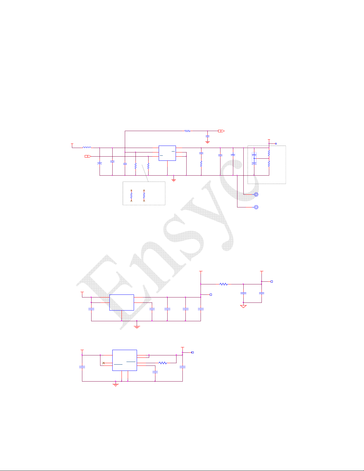
RFID UHF Short Range Controller (RF2400)
__________________________________________________________________________
6.15 POWER REGULATORS
The 5 volt input power is converted to 4.2 volts by a Li-Ion battery charger circuit U12.
This circuit provides main system power and can charge an optional battery for portable
operations. For the USB option, a super capacitor is available and supplies extra power
during transmit operations which is not typically available from the USB interface. R42
sets the current limit to 550mA for the USB version and 1000mA for the externally
powered versions. The main 4.2 volt source also powers the RF power amplifier.
+4.2V Supply
550/1000 mA
+5V
CHRGCTL3
L9 10OHM
R40 20K0
1,2,3
U12
VCC
PROG
EN
LI/CC
PAD
LTC4059EDC
7
3
BAT
2
1
GND
1,2,3
D
1,2,3
C61
C66
1uF
+
22uF
10V
1,2,3
10V
1,2,3
C62
xxx
100pF
1,2,3
xxx Alternate values for R42
2.21K = 550 mA
1.21K = 1000 mA
R42-1
1K21
1,2
4
5
6
R42
R39
10K
1,2,3
R42-2
2K21
3
D
C60
1uF
10V
1,2,3
R38
1R00
1,2,3
CHRGMON 3
C53
10nF
1,2,3
C52
C51
+
470uF
22uF
6.3V
6.3V
1,2
1,2,3
+4V2
1
R511
C534
10K
+
3
2
200mF
R510
+
3
10K
3
3
Layout: Place on
back of board
WH1
BAT +
WireHole
WH2
BAT -
WireHole
TN513
Figure 6-6 Main Power 4.2V Regulator
Two low drop-out (LDO) regulators provide the required power for various digital and
analog circuits. U13 supplies +1.8V power to the processor core and U11 supplies
+3.3V power for the processor I/O and additional controller circuitry.
+3V3
+3.3V Supply
150mA
+4V2 C519
C50
1uF
10V
1,2,3
U11
1
VIN
SDN#3BYPASS
VOUT
GND
LP2985AIM5-3.3
2
1,2,3
5
4
C49
10nF
1,2,3
C47
2u2F
10V
1,2,3
C46
22uF
6.3V
1,2,3
C48
100nF
1,2,3
R506 1R5
TN508
1,2,3
A
C44
10uF
6.3V
1,2,3
+3V3A
10nF
1,2,3
TN2
D
+1.8V Supply
+4V2
2u2F
10V
1,2,3
300mA
2
5
7
U13
IN
SET
SHDN
D
PAD
9
OUT
OUT
FAULT
CC
GND
LP3982ILD-1.8
3
1,2,3
1
4
8
6
R41 100K
33nF
1,2,3
+1V8
TN507
C65
1,2,3C59
2u2F
10VC68
1,2,3
Figure 6-7 +3.3V and +1.8V Regulator
________________________________________________________________________
Ensyc
- C
Technologies P
ONFIDENTIAL
AGE
73 11:56:13 AM
- M
ARCH
30, 2008
Page 83

Page 84

RFID UHF Short Range Controller (RF2400)
__________________________________________________________________________
7 SPECIFICATIONS
7.1 ELECTRICAL SPECIFICATIONS
7.1.1 RF Interface
RF output Frequency Range 860Mhz – 960 MHz
Transmit Power Range 0.1mW – 500mW
Receiver Sensitivity -68dBm
7.1.2 Communications Interface
Serial Interface Baud Rate 9600, 19200, 38400, 57600, 115200 baud
Digital I/0 TTL I/O levels
7.1.3 Power Supply
Power Supply Voltage 4.5Vdc – 5.5Vdc
Supply Current 1.25A max
Current Consumption
Average: 350mA
Peak: 750mA
Power Dissipation
Average: 1.75Watts
Peak: 3.75Watts
________________________________________________________________________
Ensyc
- C
Technologies P
ONFIDENTIAL
AGE
75 11:56:13 AM
- M
ARCH
30, 2008
Page 85

RFID UHF Short Range Controller (RF2400)
__________________________________________________________________________
7.1.4 Battery (optional)
Type Polymer Lithium-ion
Battery Voltage Nominal 3.7Vdc
Battery Voltage range 2.7Vdc – 4.2Vdc
Capacity 3200mAh
Note: A protection circuit in the battery prevents charging beyond 4.2V and discharging
below 2.75. Additionally, there is short circuit protection at 3A.
7.2 ENVIRONMENTAL SPECIFICATIONS
Operation Temperature Range -20ºC to 50ºC (-4ºF to -22ºF)
Storage Temperature -40ºC to 80ºC (-40ºF to 176ºF)
Relative Humidity 5% to 80% non-condensing
7.3 MECHANICAL SPECIFICATIONS
Size 2.12 x 3.36 x 0.25 in
(53.87 x 85.37 x 6.35mm)
Mounting #4-thru hole (4plcs) 1.85 x 3.08 in
(46.86 x 78.36mm)
Weight 0.8 oz (23g)
________________________________________________________________________
Ensyc
- C
Technologies P
ONFIDENTIAL
AGE
76 11:56:13 AM
- M
ARCH
30, 2008
Page 86

RFID UHF Short Range Controller (RF2400)
__________________________________________________________________________
7.4 I/O CONNECTORS
J4 – Power/Serial IO Connector
Pin Signal Description
1 +5V System power +5Vdc ±10%, 1.25A max
2 +5 RTN +5Vdc Ground
3 Signal GND Serial I/O Ground Reference
4 Host RX Serial Host Receiver (RS232 or optional TTL)
5 Host TX Serial Host Transmitter (RS232 or optional TTL)
Note: Rx/Tx are from the RF2400 perspective.
J3 – Optical Sensor Connector
Pin Signal Description
1 SensPwr 4.2V power for Opto transistor (100ohm series resistor)
2 SensSgnl Optical signal input from Optical Receiver (Emitter)
3 LED Rtn LED power return (LED Cathode) (Pulsed)
4 LEDpwr LED Power +4.2V (LED Anode)
Mating connector – Molex 87439-0500
Mating connector – Molex 87439-0400
J2 – Digital IO Connector
Pin Signal Description
1 Default Factory Default Jumper Option – (jumper to pin 2)
2 GND Reference ground for Jumper options
3 SerBoot Force Serial Boot Jumper Option- (jumper to pin 2)
4 3.3V Source power for external LED (Series 150 ohm resistor)
5 Port0 Bi-directional Digital IO Port0
6 GND Reference ground for Digital IO Ports
7 Port1 Bi-directional Digital IO Port1
8 ActLedPwr Activity LED power (3.3V with series 150ohm)
9 ActLedRtn Activity LED return (Buffered Driver)
10 PwrLedPwr Power LED power (3.3V with series 150ohm)
11 PwrLedRtn Power LED return (Buffered Driver)
Mating connector – Molex 87439-1100
________________________________________________________________________
Ensyc
- C
Technologies P
ONFIDENTIAL
AGE
77 11:56:13 AM
- M
ARCH
30, 2008
Page 87

RFID UHF Short Range Controller (RF2400)
__________________________________________________________________________
Figure 7-1 RF2400 Mechanical Assembly
________________________________________________________________________
Ensyc
- C
Technologies P
ONFIDENTIAL
AGE
78 11:56:13 AM
- M
ARCH
30, 2008
Page 88

RFID UHF Short Range Controller (RF2400)
__________________________________________________________________________
________________________________________________________________________
Ensyc
- C
Technologies P
ONFIDENTIAL
AGE
79 11:56:13 AM
- M
ARCH
30, 2008
Page 89

 Loading...