

Energy Star 200W6CB, 200W6CB27, 200W6CS, 200W6CS00 Service Manual
Horizontal frequencies
30 - 93KHz
Service
Service
Service
TABLE OF CONTENTS
Published by BCU Monitors Printed in Suzhou Copyright reserved Subject to modification S Mar. 15 2005
Description Page
Important Safety Notice ------------------------------2
Technical Data ------------------------------------- 3~4
Front Control & Connections---------------------- 5~6
On-screen Display(OSD)------------------------------7
Aging Mode ------------------------------------------- 8
Warning Message------------------------------------- 9
Pixel Defect Policy------------------------------------10
Wiring Message----- ---------------------------------14
Block Diagram----------------------------------------15
Display Adjustments ------------------------------- 11
Mechanical Instructions-------------------------12~13
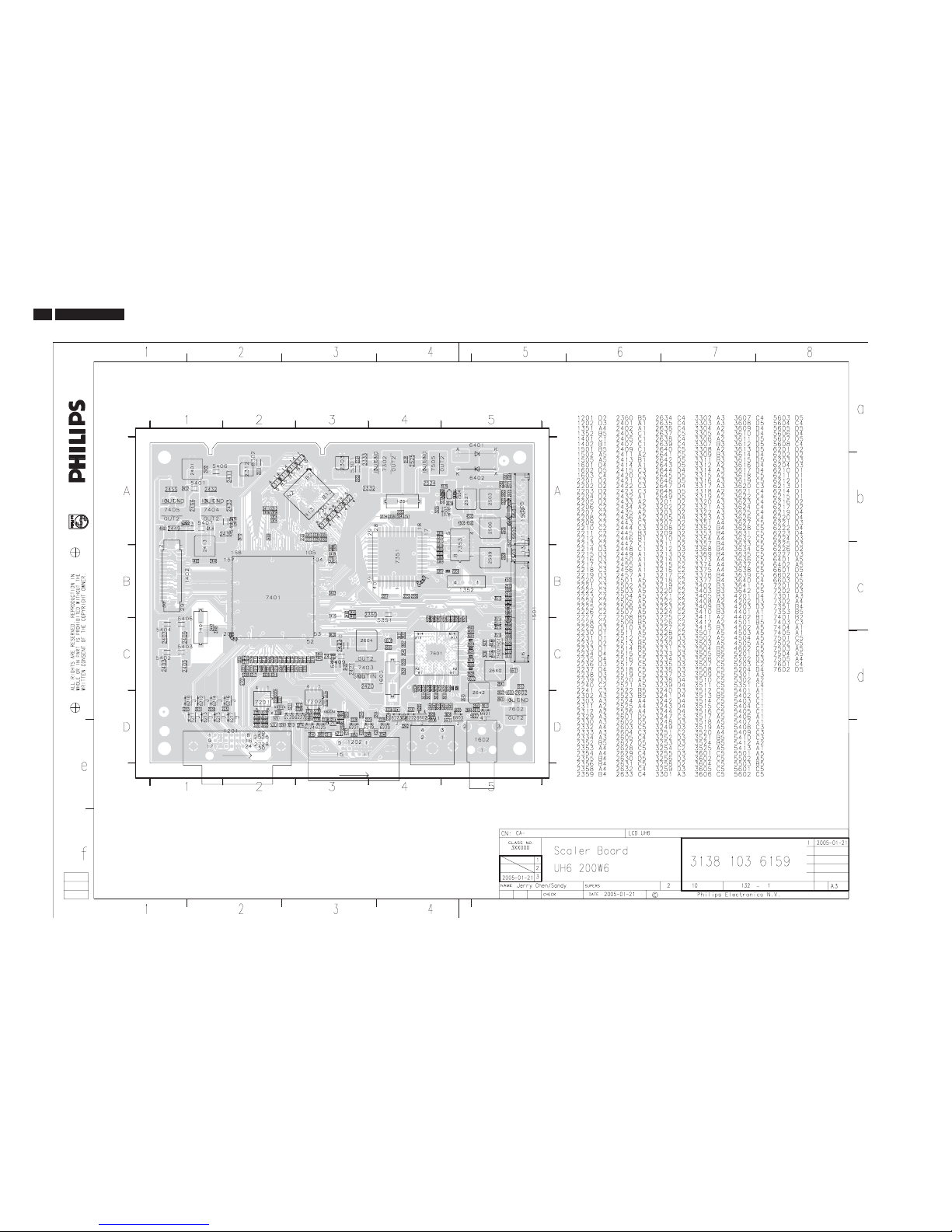
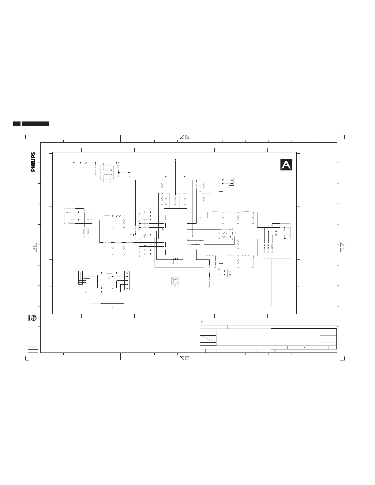
Scaler Diagram & C.B.A. ------------------------16~23
Audio + Control Diagram & C.B.A. ------------24~25
USB Schematic Diagram & C.B.A. ------------------26
Description Page
Power Schematic Diagram & C.B.A. -----------27~30
Repair Tips -------------------------------------- 71~72
Repair Flow Chart -------------------------------73~75
Safety Test Requirement --------------------------- 76
Different Parts List ---------------------------------- 77
Exploded View--------------------------------------- 31
Spare parts list --------------------------------- 32~33
Recommended parts list --------------------------- 34
General product specification----------------- 35~59
Trouble Shooting ------------------------------- 69~70
ISP Instruction --------------------------------- 60~61
DDC Instructions ------------------------------- 62~66
DDC HEX Data -------------------------------------- 68
Chassis: UH6
REFER TO BACK COVER FOR IMPORTANT SAFETY GUIDELINES
CAUTION: USE A SEPARATE ISOLATION TRANSFORMER FOR THIS UNIT WHEN SERVICING.
ANY PERSON ATTEMPTING TO SERVICE THIS CHASSIS MUST FAMILIARIZE HIMSELF WITH THE CHASSIS
AND BE AWARE OF THE NECESSARY SAFETY PRECAUTIONS TO BE USED WHEN SERVICING ELECTRONIC
EQUIPMENT CONTAINING HIGH VOLTAGES.
SAFETY NOTICE
GB
3138 106 10458
20 inch TFT LCD Colour Monitor
«
200W6CB/27
200W6CS/00

Important Safety Notice
2
FOR PRODUCTS CONTAINING LASER :
Invisible laser radiation when open.
AVOID DIRECT EXPOSURE TO BEAM.
Use of controls or adjustments or
performance of procedures other than
those specified herein may result in
hazardous radiation exposure.
The use of optical instruments with this
product will increase eye hazard.
DANGER-
CAUTION-
CAUTION-
TO ENSURE THE CONTINUED RELIABILITY OF THIS
PRODUCT, USE ONLY ORIGINAL MANUFACTURER'S
REPLACEMENT PARTS, WHICH ARE LISTED WITH
THEIR PART NUMBERS IN THE PARTS LIST SECTION
OF THIS SERVICE MANUAL.
200W6 LCD
Proper service and repair is important to the safe,
reliable operation of all Philips Consumer Electronics
Company** Equipment. The service procedures
recommended by Philips and described in this service
manual are effective methods of performing service
operations. Some of these service operations require
theuseoftoolsspeciallydesignedforthepurpose.The
specialtoolsshouldbeusedwhenandas
recommended.
Itisimportanttonotethatthismanualcontains
various CAUTIONS and NOTICES which should be
carefully read in order to minimize the risk of personal
injury to service personnel. The possibility exists that
improper service methods may damage the equipment.
It is also important to understand that these
CAUTIONS and NOTICES ARE NOT EXHAUSTIVE.
Philips could not possibly know, evaluate and advise
theservicetradeofallconceivablewaysinwhich
service might be done or of the possible hazardous
consequences of each way. Consequently, Philips has
not undertaken any such broad evaluation. Accordingly,
aservicerwhousesaserviceprocedureortoolwhich
is not recommended by Philips must first satisfy
himself thoroughly that neither his safety nor the safe
operationoftheequipmentwillbejeopardizedbythe
service method selected.
* *Hereafter throughout this manual, Philips Consumer
Electronics Company will be referred to as Philips.
WARNING
Critical components having special safety
characteristics are identified with a by the Ref. No.
in the parts list and enclosed within a broken line*
(where several critical components are grouped in one
area)alongwiththesafetysymbol onthe
schematics or exploded views.
Use of substitute replacement parts which do not have
the same specified safety characteristics may create
shock, fire, or other hazards.
Under no circumstances should the original design be
modified or altered without written permission from
Philips. Philips assumes no liability, express or implied,
arising out of any unauthorized modification of design.
Servicer assumes all liability.
*BrokenLine
Take care during handling the LCD module with
Backlight unit
- Must mount the module using mounting holes
arranged in four corners.
-Donotpressonthepanel,edgeoftheframe
stronglyorelectricshockasthiswillresultin
damage to the screen.
-Donotscratchorpressonthepanelwithanysharp
objects,suchaspencilorpenasthismayresultin
damage to the panel.
- Protect the module from the ESD as it may damage
the electronic circuit (C-MOS).
- Make certain that treatment person s body are
grounded through wrist band.
-Donotleavethemoduleinhightemperatureandin
areasofhighhumidityforalongtime.
-Avoidcontactwithwaterasitmayashortcircuit
within the module.
- If the surface of panel become dirty, please wipe it
offwithasoftmaterial.(Cleaningwithadirtyor
rough cloth may damage the panel.)

3
200W6 LCD
Technical Data
Technical Specifications*
LCD PANEL
- Type: TFT LCD
- Screen size: 20.1" / 51cm
- Pixel Pitch: 0.258 x 0.258mm
- LCD Panel type: 1680 x 1050 pixels
R.G.B. vertical stripe
Anti-glare polarizer, hard coated
- Effective viewing area: 433.44 x 270.9 mm
- Display Colors: 8 bits interface (16.7M colors)
SCANNING
Vertical refresh rate 56Hz-85Hz
Horizontal Frequency 30kHz-93kHz (Analog input)
VIDEO
- Video dot rate: 165 MHz
- Input impedance
Video: 75 ohm
Sync : 2K2 ohm
- Input signal levels: 0.7 Vpp
- Sync input signal:
Separate sync
Composite sync
Sync on green
- Sync: polarities Positive and negative
- S-Video: Y input 1.0Vpp, C input 0.3Vpp, 75ohm input impedance
- CVBS Composite, 1.0Vpp, 75 ohm input impedance
- Video interface
D-Sub (Analog)
DVI-D (Digital)
AUDIO-IN
- Input signal level :0.7 Vpp
- Headphone out signal level: 20mW x 2, 32
- Input signal connector :3.5mm mini jack
- Loudspeaker: 4W Stereo Audio
(2W/channel RMSx2, 200Hz-12kHz, 4 ohm,THD=10%)
Optical characteristics
- Contrast ratio: 600:1 (typ).
- Brightness: 300 cd/m2 (typ.)
- Peak contrast angle 6 o'clock
- White Chromaticity:
x: 0.283 y: 0.297 (at 9300 K)
x: 0.313 y: 0.329 (at 6500 K)
- Viewing Angle:
(C/R>10)
Upper >88 (typ.)
Lower >88 (typ.)
Left >88 (typ.)
Right >88 (typ.)
- Response tim
e
16 ms (typ.)
1.
Pin
No.
Signal
Assignment
Pin
No.
Signal
Assignment
Pin
No.
Signal
Assignment
1
T.M.D.S.
Data2-
9
T.M.D.S.
Data1-
17 T.M.D.S. Data0-
2
T.M.D.S.
Data2+
10
T.M.D.S.
Data1+
18
T.M.D.S.
Data0+
3
T.M.D.S.
Data2/4 Shield
11
T.M.D.S.
Data1/3
Shield
19
T.M.D.S.
Data0/5 Shield
4 No connect 12 No connect 20 No connect
5 No connect 13 No connect 21 No connect
6 DDC Clock 14 +5V Power 22
T.M.D.S. Clock
Shield
7 DDC Data 15
Ground (for
+5V)
23 T.M.D.S. Clock+
8 No connect 16
Hot Plug
Detect
24 T.M.D.S. Clock-
Pin Assignmen t
The digital only connector contains 24 signal contacts organized in
three rows of eight contacts. Signal pin assignments are listed in the
following table:
2. The15-pin D-sub connector (male) of thesignal cable:
Pin
No.
Assignment
Pin
No.
Assignment
1 Redvideoinput 9 +5V
2
Greenvideo
input/SOG
10 Logic ground
3 Blue videoinput 11 Ground
4 Ground 12
Serial dataline
(SDA)
5 No connect 13 H. Sync / H+V
6 Redvideoground 14
V. Sync (VCLK for
DDC)
7
Greenvideo
ground
15
Data clock line
(SCL)
8 Blue video ground
Physical Specifications
- Dimension (WxHxD) : 478 x 423.5 x235 mm (incl. Pedestal)
- Weight : 7.6 Kg
- Tilt / Swive : -5 ~ 25 / 125
- Power supply : 100 240 VAC, 60 - 50 Hz
- Power consumption : 50 W* (typ.)
-Temperature : 5 C to 40 C (operating)
20 C to 60 C (storage)
- Relative humidity :20% to 80%
- System MTBF : 50K hrs (excluding CCFL 40K hrs)
- Cabinet color : 200W6CB: Black
200W6CS: Silver
- Altitude
storage/shipment:
operating :
0 - 40,000 feet (12,192m)
0 - 12,000 feet (3657.6m)
Technical Data
4
200W6 LCD
Auto Power Saving
If you have VESA DPMS compliance display card or software
installed in your PC, the monitor can automatically reduce its power
consumption when not in use. If an input from a keyboard, mouse or
other input device is detected, the monitor will 'wake up'
automatically. The following table shows the power consumption
and signaling of this automatic power saving feature:
Resolution & Preset Modes
Maximum
1680 x 1050 at 75Hz(analog input)
1680 x 1050 at 60Hz(digtal input)
Recommended 1680 x 1050 at 60Hz * at DVI digital input
39 user definable modes
15 factory preset modes:
H. freq (kHz) Resolution V. freq (Hz)
31.469 640x350 70.086
31.469 720x400 70.087
31.469 640x480 59.940
35.000 640x480 67.000
37.500 640x480 75.000
35.156 800x600 56.250
37.879 800x600 60.317
46.875 800x600 75.000
48.363 1024x768 60.004
60.023 1024x768 75.029
68.700 1152x870 75.000
63.981 1280x1024 60.020
79.976 1280x1024 75.025
75.0 1600x1200 60
65.29 1680x1050 60.0
Power Management Definition
VESA Mode Video H-sync V-sync Power Used LED color
Active ON Yes Yes <68W Green
Sleep OFF No No <1.5W Amber
Switch Off OFF - - <1.5W OFF
R
R
R
This monitor is ENERGY STAR compliant. As an ENERGY STAR Partner,
PHILIPS has determined that this product meets the ENERGY STAR
guidelines for energy efficiency.
Optimizing Performance
·
For best performance, ensure that your display
settings are set at 1680 x 1050 @60Hz
Note: You can check the current display settings
by pressing the 'OK' button once. Go into the
Product Information. The current display mode is
shown on the i tem called RESOLUTION

5
200W6 LCD
Front Control & Connections
Front View Product Description
Rear View
AccessoryPack
Unpackall the parts.
Power cord VGA signalcable
PC audio cable
(lime)
Mac adaptor
(optional)
DVI cable
USB cable USB
c able
EDFUpack EDFUpac k
1
Toswitchmonitor's power On andOff
2
Power LED
3
To access OSD menu
4
To adjust the OSD
5
To adjust brightness of the display
6
To adjust the OSD
7
VOLUME
To adjust speaker volume
8
AUTO
Automaticallyadjust the horizontal
position,vertical position,phase and
clock setting
1Kensington anti-thief lock
2VGAinput
3DVI-Dinput
4PC audio input
5Earphone jack
6AC power input
7USBupstream port
8USBdownstream port
Front Control & Connection
6
200W6 LCD
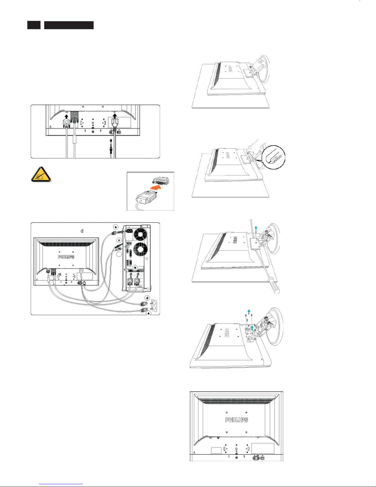
Connect to PC
Connect the power cord, DVI and audio cable
to the back of the monitor firmly. (Philips has
pre-connected VGA cable for the first
installation.)
If you use an Apple
Macintosh
TM
, you need to
connect the special Mac
adapter to one end of the
monitor signal cable.
Connect the cables to the back of your
computer by following these steps:
(a)
Turn off your computer and unplug its
power cord.
(b)
Connect the VGA or DVI cable to the
video connector.
(c) Connect the audio cable.
(d)
Plug the power cord of the computer and
the monitor into a nearby outlet.
(e)
Turn on your computer and monitor. If
the monitor displays an image,
installation is complete.
1) Place monitor face down on a safe surface.
2) Remove the cable cover.
3) Remove the base cover.
VESA Standard Mounting
4) Unscrew the 5 screws at the base.
5) VESA mounting holes
7
200W6 LCD
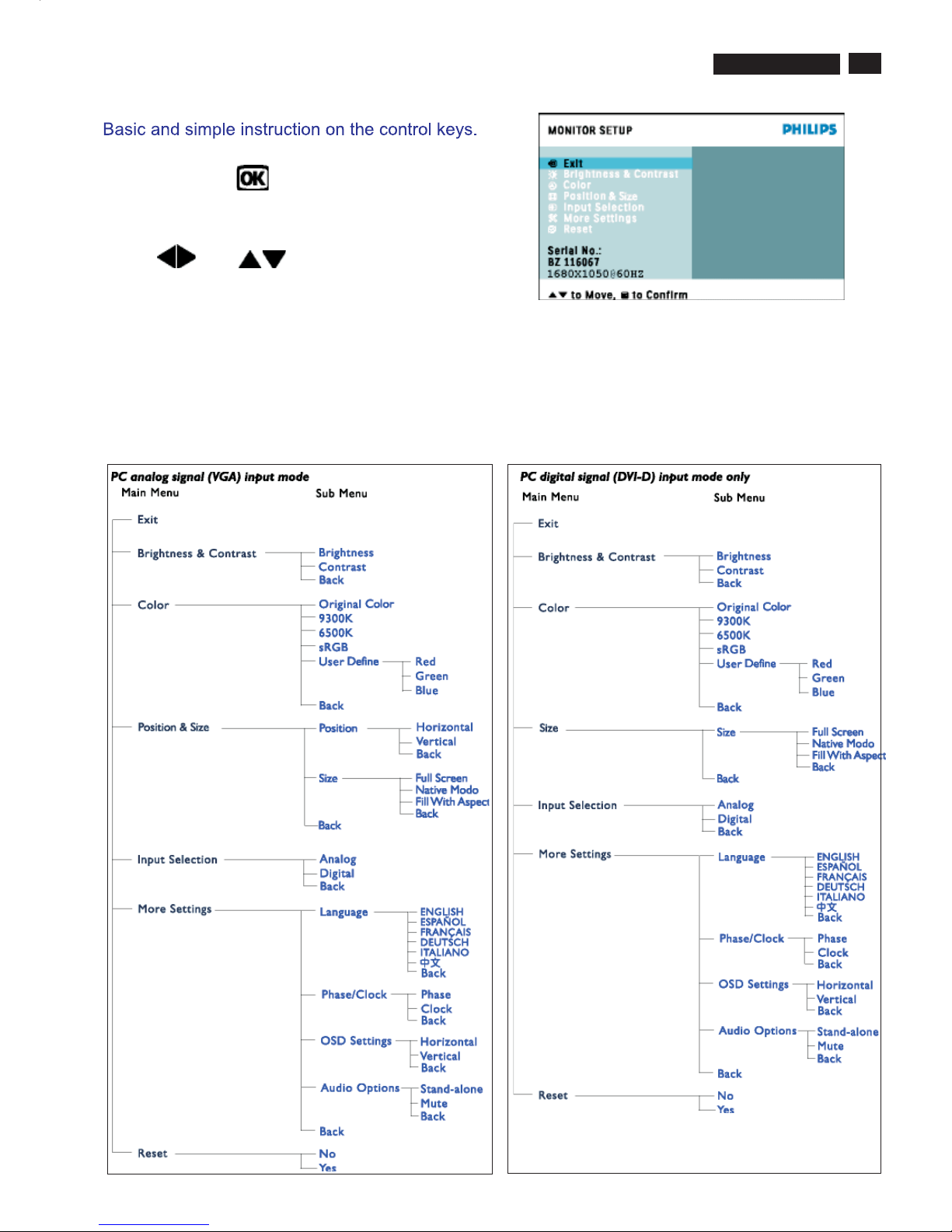
On Screen Display
When you press the button on the front control of
your monitor, the On-Screen Display (OSD) Main
Controls window will pop up and you can then start
making adjustments to your monitor's various features.
Use the
or the keys to make your
adjustments.
The OSD Tree
Below is an overall view of the structure of the On-Screen Display. You can use this as a reference when you want to
work your way around the different adjustments later on.
OSD Lock/Unlock, Aging Mode
8
200W6 LCD
Front Control Panel
To Lock/Unlock OSD FUNCTION(User Mode)
The OSD function can be locked by pressing"OK"button(1) for more
than 10 seconds, the screen shows following windows for 3 seconds.
Everytime when you press"AUTO" or "OK" button, this message appears on the screen automatically.
ATTENTION SIGNAL
OSD MAIN CONTROLS UNLOCKED
Unlock OSD function
Locked OSD function can be released by pressing "OK" button for more
than 10 seconds again
ATTENTION SIGNAL
OSD MAIN CONTROLS LOCKED
NO VIDEO INPUT
This screen appears if there is no video signal input. Please check that
the signal is properly connected to the video card of PC and make sure
PC is on
ATTENTION SIGNAL
CHECK CABLE CONNECTION
CANNOT DISPLAY THIS VIDEO MODE..
This screen warns when the input frequency from the computer is not
a standard video mode or out of the monitor's scanning range.
Please change the display mode of the operating software in the computer(i.e.windows) to 1680*1050@60HZ for best display results.
ATTENTION SIGNAL
CANNOT DISPLAY THIS VIDEO
MODE,CHANGE COMPUTER DISPLAY
INPUT TO 1680*1050@60HZ
I
WAIT FOR AUTOMATIC ADJUSTMENT
This screen appears when you press the "AUTO" buttons at the same
time. It will disappear when the monitor is properly adjusted
ATTENTION SIGNAL
WAITING FOR AUTOMATIC ADJUSTMENT
Access Aging.. Mode
Step1:TurnoffLCDmonitor, and disconnect Interface Cable
between Monitor and PC.
Step 2 : [Push AUTO " " & " " buttons at the same time and
hold it]+[Press power " " button until comes out " AGING screen"
] => then release all buttons.
Bring up:
AGING...
After 10 seconds, bring up:
After 3 seconds, bring up:
AGING...
After 10 seconds, bring up:
----------
---------repeatly
Connect Signal cable again=> go back to normal display
9
200W6 LCD
Warning Message Table
Item Attention Signals Display Time Condition
1 CANNOT DISPLAY THIS VIDEO MODE,
CHANGE COMPUTER DISPLAY
INPUTTO 1680x1050 @ 60HZ
30 mins This warning appears when theinput signal from your
computer is not inastandardvi deomode orisout of the
monitor’sscanning range.After 30 mins,monitorenters
sleeping mode.
2 NO VIDEO INPUT 30 mins This message appears when there is no signal input
while power on.After 30 mins,monitorenters sleeping
mode.
3 CHECK CABLE CONNECTION 30 mins This message appears when a signal cable is
disconnectedwhile monitorisworking.After 30 mins,
monitorenters sleeping mode.
4 ENTERING SLEEP MODE 3 secs This message appears when monitorisabout to enter
power saving mode.
5 WAITING FOR AUTOMATIC ADJUSTMENT till auto adjustment
finished
This message is displayedwhen theauto adjustment
buttonispressed. It disappears when automatic
adjustmentsarecompleted.
6 USE 1680x1050 FOR BEST RESULT On top of OSD
main menu
The message will show up atthe top of the OSD main
menu in redcolor when theinput resolutionisnot the
1280x1024.
7 OSD MAIN CONTROLS LOCKED 3 secs /or Till
"OSD MAIN
CONTROLS
UNLOCKED"
appear
This message will appear 3 seconds to indicate the OSD
MAIN CONTROLS status when to lock or un-lock it by
pressing “MENU(OK)” button for more than 10 seconds
while there is video input from PC. This function provides
thealternative thatuser can lock all the OSD main
controlincase user don’twantthe FOS performance
setting to be changed, forinstance,during commercial
exhibition.
8 OSD MAIN CONTROLS UNLOCKED 3 secs This message will appear 3 seconds to indicate the OSD
MAIN CONTROLS status when to un-lock it bypressing
“MENU(OK)”button for more than 10 seconds while
there is video input from PC.
9 the window of "OSD MAIN CONTROLS" 60 secs This message will appear when the “O K ” buttonis
pressed.
10 the window of "BRIGHTNESS" 60 secs This message will appear when the BRIGHTNESS
buttonispressed.
11 The window of “VOLUME” 60 secs This message will appear when the”O K ” buttonis
pressed
12 “S E L E C TED INPUT NOT AVAILABLE” 3 secs This message will appear 3 seconds to indicate the
SIGNAL SOURCE status when change the signal source
but is not foundwhile there is video input from PC
Pixel Defect Policy
10
200W6 LCD
Philips' Flat Panel Monitors Pixel Defect Policy
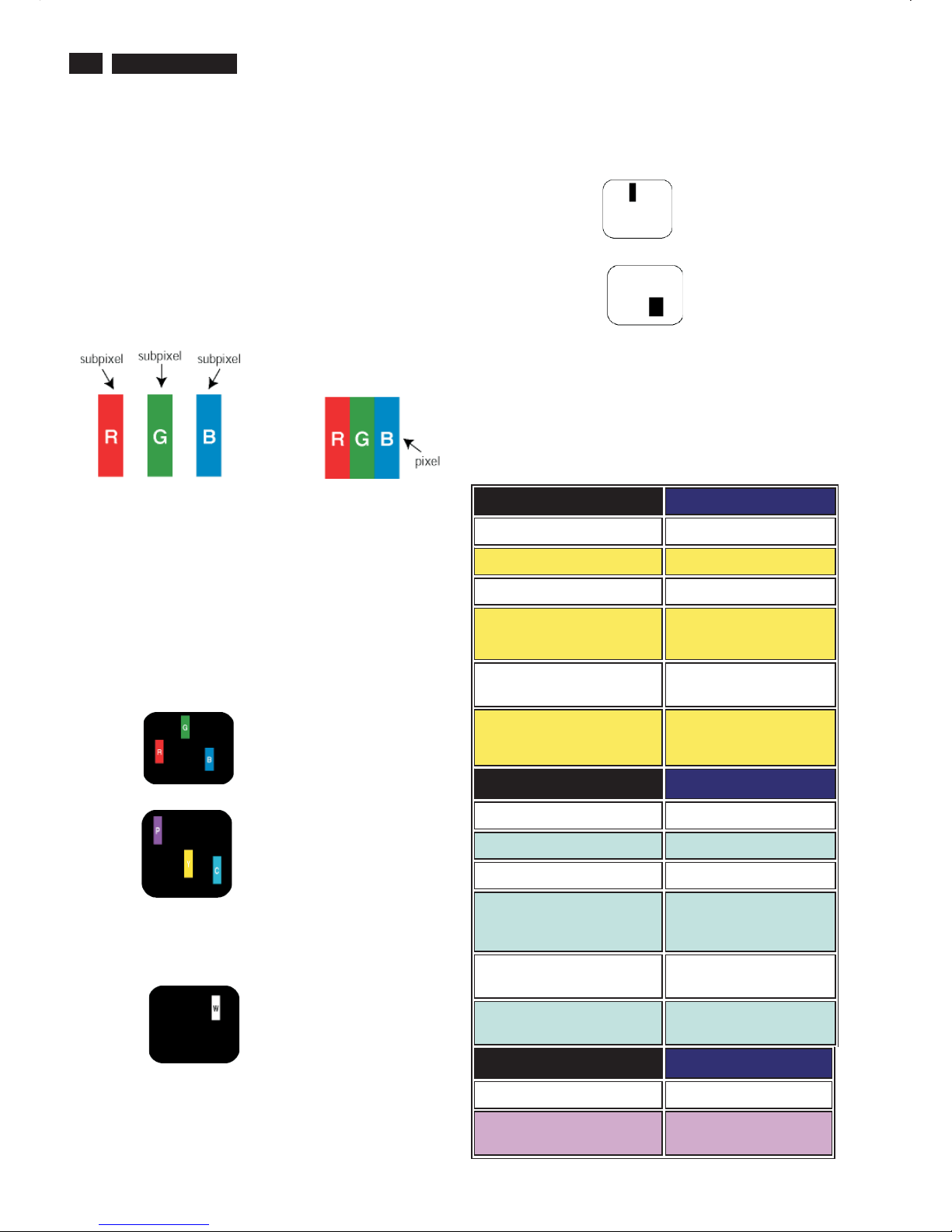
Pixels and Subpixels
Types of Pixel Defects
Philips strives to deliver the highest quality products. We use some of
the industry's most advanced manufacturing processes and practice
stringent quality control. However, pixel or subpixel defects on the TFT
LCD panels used in flat panel monitors are sometimes unavoidable.
No manufacturer can guarantee that all panels will be free from pixel
defects, but Philips guarantees that any monitor with an unacceptable
number of defects will be repaired or replaced under warranty.
This notice explains the different types of pixel defects and defines
acceptable defect levels for each type. In order to qualify for repair or
replacement under warranty, the number of pixel defects on a TFT LCD
panel must exceed these acceptable levels.
For example, no more than 0.0004% of the subpixels on a 15" XGA
monitor may be defective. Furthermore, Philips sets even higher quality
standards for certain types or combinations of pixel defects that are
more noticeable than others. This policy is valid worldwide .
A pixel, or picture element, is composed of three subpixels in the
primary colors of red, green and blue. Many pixels together form an
image. When all subpixels of a pixel are lit, the three colored subpixels
together appear as a single white pixel. When all are dark, the three
colored subpixels together appear as a single black pixel.
Other combinations of lit and dark subpixels appear as single pixels of
other colors.
Pixel and subpixel defects appear on the screen in different ways.
There are two categories of pixel defects and several types of subpixel
defects within each category.
Bright Dot Defects Bright dot defects appear as pixels or subpixels that
are always lit or "on".
These are the types of bright dot defects:
One lit red, green or blue subpixel
Two adjacent lit subpixels:
- Red + Blue = Purple
-Red+Green=Yellow
- Green + Blue = Cyan (Light Blue)
Three adjacent lit subpixels
(one white pixel)
Black Dot Defects
Proximity of Pixel Defects
Pixel Defect Tolerances
Black dot defects appear as pixels or subpixels that are always dark or
"off".
These are the types of black dot defects:
One dark subpixel
Two or three adjacent dark subpixels
Because pixel and subpixels defects of the same type that are nearby
one another may be more noticeable, Philips also specifies tolerances
for the proximity of pixel defects.
In order to qualify for repair or replacement due to pixel defects during
the warranty period, a TFT LCD panel in a Philips flat panel monitor
must have pixel or subpixel defects exceeding the tolerances listed in
the following tables.
BRIGHT DOT DEFECTS ACCEPTABLE LEVEL
MODEL 200W6
1 lit subpixel 3 or fewer
2 adjacent lit subpixels 1 or fewer
3 adjacent lit subpixels
(one white pixel)
0
Distance between two
bright dot defects*
15 mm or more
Total bright dot defects of
all types
3 or fewer
BLACK DOT DEFECTS
ACCEPTABLE LEVEL
MODEL 200W6
1 dark subpixel 5 or fewer
2 adjacent dark subpixels 2 or fewer
3 adjacent dark subpixels 0
Distance between two
black dot defects*
15 mm or more
Total black dot defects of
all types
5 or fewer
TOTAL DOT DEFECTS
ACCEPTABLE LEVEL
MODEL 200W6
Total bright or black dot
defects of all types
5orfewer
11
200W6 LCD
Display Adjustment
Alignment procedure
1. Turn on the LCD monitor.
2.Turn on the Timing/pattern generator. See Fig.1
3. Preset LCD color Analyzer CA-110
-Remove the lens protective cover of probe CA-A30.
-Set measuring/viewing selector to measuring position for reset
analyzer.(zero calibration) as Fig.2
- Turn on the color analyzer (CA-110)
-Press 0-CAL button to starting reset analyzer.
Fig. 1
Fig. 2
Clear imageClear image
Measurement/viewing selectorMeasurement/viewing selector
4. Access Factory Mode
How to get into Factory Mode Menu
Step1:
Turn off monitor.
Step2:
[Push AUTO " " & OK " " buttons at the same time and hold it]
+[Press power " " button untill comes out "Windows screen" ]
=> then release all buttons
Step3:
Press OK " " button, bring up Factory mode indication as shown
in Fig3.
Fig. 3
Step4:
- Press button, then select factory mode indicator by"" ""
button
- Press" " button to bring up submenu windows as below:
5.Display
Press " " or " " button to select . Change the value
by " " or " " key until the X,Y co-ordinates as below
Fig.5
HUDSON6 200W6 V200 050309
Factory Mode indicator
Cover (black)Cover (black)
Measurement viewing selectorMeasurement viewing selector
5.1 Auto color adjustment (B)
Apply a 1280x1024/60Hz signal with Black and white levels pattern, set
brightness control at 100%, and contrast control at 50%.AdjusttheR.
G. B offset, and gain to calibrate the color smoothly and 64-gray level
distinguishable. Check all factory pre-setting modes.
5.2 Adjustment of WHITE-D (B)
Apply a 1280*1024 / 60Hz signal with white pattern, set brightness
control at 100%, and contrast control at 50%. Adjust the R, G, B SubGain, for the screen center, the 1931 CIE chromaticity (X, Y) co-
ordinates shall be;
Use Minolta CA-110 for colour coordinates and luminance check.
Luminance is > 200 Nits in the center of the screen when
brightness at 100% and contrast set to 100%.
5.3 Adjustment of sRGB
Apply a 1280*1024 / 60Hz signal with white pattern, set brightness
control at 100%, and contrast control at 50%. Adjust the R, G, B SubGain, for the screen center, the 1931 CIE chromaticity (X, Y) coordinates shall be;
sRGB
x(center) 0.313 +/- 0.008
y(center) 0.329 +/- 0.008
Ynits 180 ± 10
5.4 Factory Preset (B):
5.4.1
After finished all the adjustment, set:
OSD Default Setting:
Brightness: 100%
Contrast: 50%
Adjust size: Full screen
Language: English
Colour: 6500K for IMAGE MANAGEMENT
OSD position: middle of the LCD screen
Input Selection: Default as PC VGA(D-sub)
Volume: 50
5.4.2
In Factory mode default setting :
SECURITY : OFF
SUB-BRI :55 255 (Fix)
SUB-CON : 78 128 178 (Fix)
PANEL: LG20 IDX 100
9300
o
K 6500oK
x (center) 0.283+/-0.008 0.313 +/- 0.008
y (center) 0.297 +/- 0.008 0.329 +/- 0.008
Fig. 4
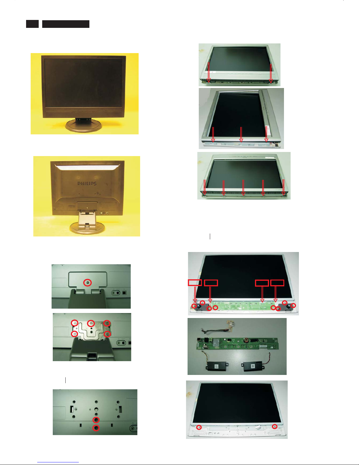
Mechanical Instructions
12
200W6 LCD
Front View
Back View
Step1. Remove the base as shown in Fig. 3-4
-Remove the screw as shown in Fig.3, then remove the hinge cover
-Remove the five screws as shown in Fig.4,then remove the base
Fig.1
Fig.2
Fig.3
Fig.4
Fig.5
Step2. Remove the Front Bezel
-Remove the two screws as shown in Fig.5
-Use the thin " " screw driver to open the clicks as shown
in Fig.6-8.
Step3.Remove the BacK cover
- Remove the eight threws as shown in Fig.9
- Disconnect 1904,1912,1911,1931 from control board as shown
in Fig.9 & Fig.10
- Remove the two screws as shown in Fig.11
- Use the thin " " type screw driver to open the clicks as shown in
Fig.12
Fig.6
Fig.8
Fig.7
Fig.9
Fig.10
1904
Fig.11
1912
1931
1911
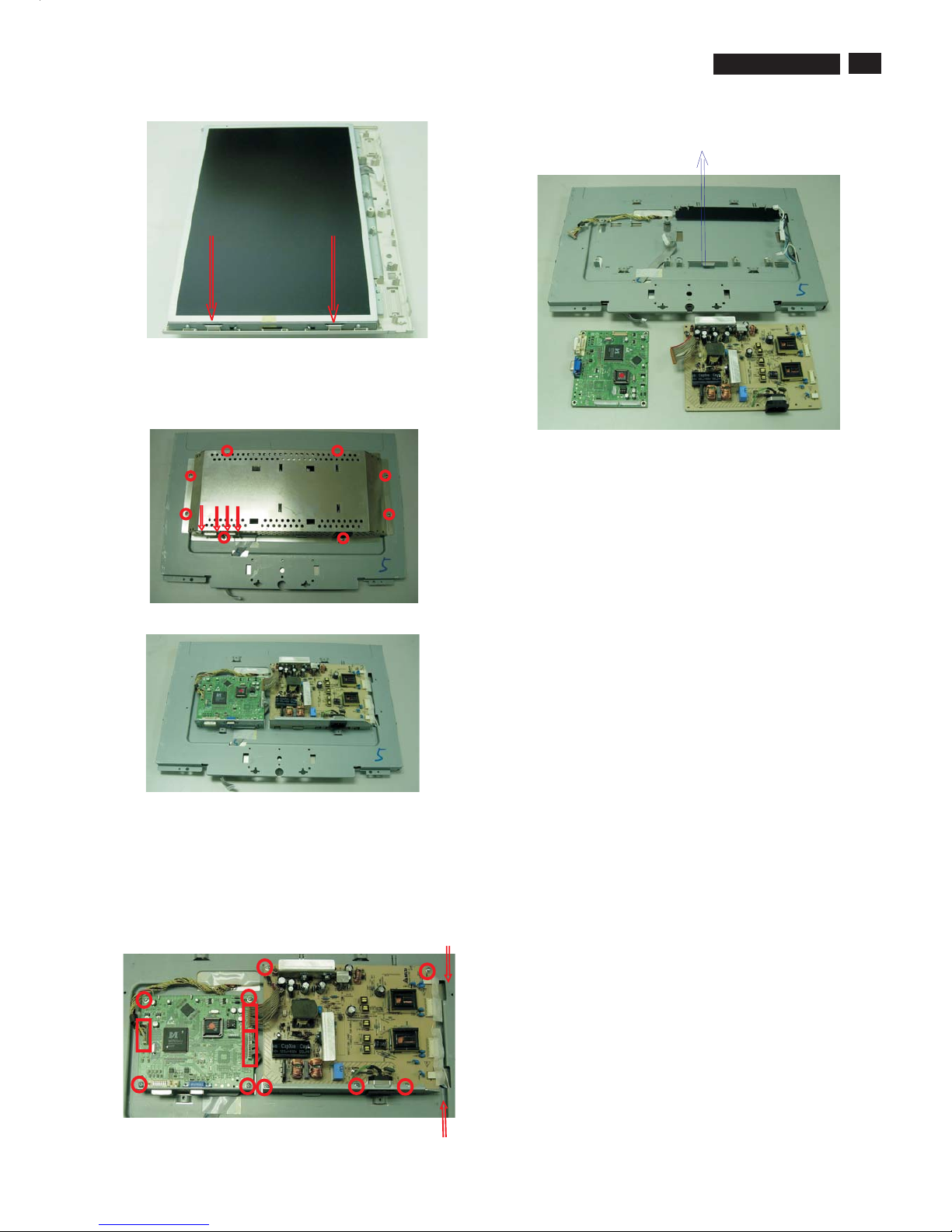
13
200W6 LCD
Mechanical Instructions
Step4. Remove the Matel frame board
- Remove the eight screws as shown in Fig.13
- Disconnect D-SUB & DVI hexagonal screws as shown in Fig.13
- Remove the matel frame board as shown in Fig.14
Fig.12
Fig.13
Step 5. Remove the sclar and power board.
- Remove the screws as shown in Fig.15
- Disconnect the 1501,1502,1402 and 4 backlight cables
as shown in Fig.15
- Remove the scaler and power board as shown in Fig.16
**************************************************************************************
***************************************************************************************
In warranty, it is not allowed to disassembly the LCD panel, even the
backlight unit defect.
Out of warranty, the replacement of backlight units is a correct way
when the defect is caused by backlight (CCFL, Lamp).
Fig.14
Fig.15
4 backlight cables
1501 to Control board
1502 to Power board
1402 to Pane
l
Panel
Fig.16
Wiring Diagram
14
200W6 LCD
Block Diagram
15
200W6 LCD
200W6 System Block
200W6 System Block
•
AC-DC Power supply
Inverter and
DC-DC converter
(200mm x 150mm)
Scalar(LVDS interface)
Dual input
(132 mm x 110mm)
D_SUB
AC
input
Connector
Connector
Connector
Connector
Connector
30 Pin wire harness(LVDS)
RGB//DE
/Hsync/Vsync
Connector
Connector
DVI
30 pin wafer
Panel
Panel Backlight (3 CCFL
)
Panel Backlight (3 CCFL
)
S_Video
CVBS
(Reserve S_Video and CVBS)
Audio + Control
Panel Vcc(12V for
LPL , 5V for AU)
USB Plug
PC_USB Hub
USB_Device
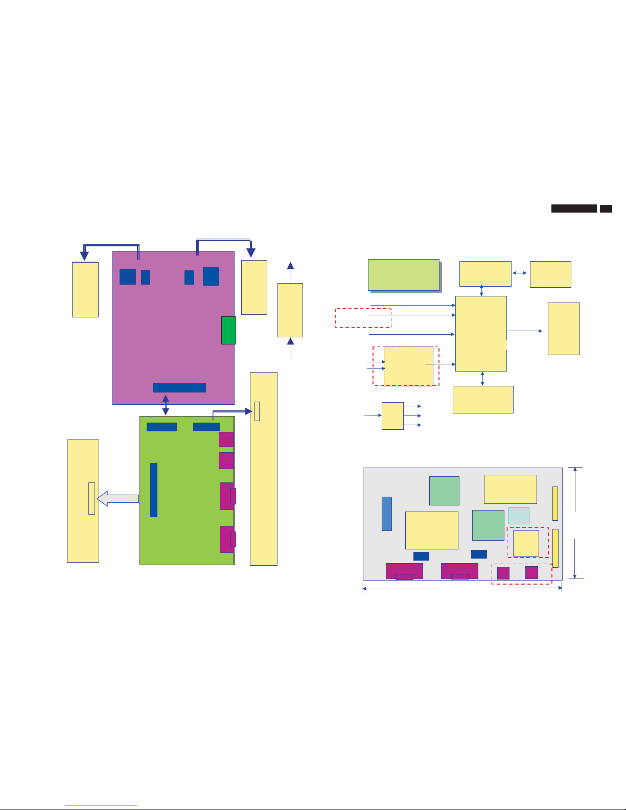
200W6 Scalar Board Block Diagram
200W6 Scalar Board Block Diagram
• To use M-star Scaler
MCU
NT68F631A
DDR
K4D263238A
Dsub
DVI_A
(Reserve)
DVI_D
LVD S
RGB/Hsync/
Vsync)
E2PROM
M24C16
Specification :
1 x Analog: 1600 x 1200 / 60Hz
1 x Digital: 1600 x 1200 / 60Hz
1xCVBS,1xS-Video(Reserve)
Specification :
1 x Analog: 1600 x 1200 / 60Hz
1 x Digital: 1600 x 1200 / 60Hz
1xCVBS,1xS-Video(Reserve)
Video
Decoder
SAA7119
CVBS
S-video
DC
to
DC
5V
3.3V
2.5V
1.8V
(Reserve)
Panel
Panel Vcc
LPL:12V
AU:5V
MST9251A for
1A+1D no
Video
.
200W6 Scalar Board Placement
132 mm
Scaler IC
MST9251A 0r 6251A
Power
13 Pin
LVDS 2*15P interface connector
128M DDR
(K4D263238A)
ToAudio & control board
16 pin
110 mm
EEP
ROM
D_SUB
DDC
DVI
DDC
S_Video
CVBS
CPU
(NT68F631A)
Video decoder
SAA7119
Power regulator
and LC filter
Scaler Schematic Diagram - 1
16
200W6 LCD
17
200W6 LCD
Scaler Schematic Diagram - 2
SCL
ADR
0
1
2SDA
WC
2
O
RSTB
1
PWM<0:1>
SDA0:1
SCL0:1
INTE<0:1>
ADC<0:3>
6
1
1
2
PB
PD<0:6>
T<0:1>
OSC
GND
VCC
PA
PATTO
VSYNCI
HSYNCO
7
34
35
P
TXD
RXD
I
3
4
5
6
7
5
4
CLMPO
HALFI
VSYNCO
PE
0
3
4
3
HSYNCI
HALFO
2
6
0
PC
31
30
1
0
5
PWM<2:9>
7
0
C
EXCEPT 1352 WERE CHIP COMPONENTS.
5351 A4
3369 A6
3370 B8
3371 B7
3372 B7
I423 D6
I424 D6
I426 D6
I427 D6
H
I
J
5 11
4
G
F
I444 C8
I445 C8
I446 A7
I447 A7
3352 D4
3353 C2
3354 D4
3355 C4
3356 C3
3357 C3
3358 C6
3359 C4
3360 C6
3361 D7
3364 D7
3376 C9
3377 C7
H
Alle rechte
n voorbehouden.V
erveelvuldiging, geheel
of
gedeeltelijk, isniet toegestaandanmet schriftelijke
U27 C4
U28 D6
U29 A7
U75 C6
U76 D6
U79 C4
3373 C8
3374 C8
3375 C9
6
1351 B3
1352 A7
2351 B5
2352 D2
2353 B3
2354 B4
2355 E4
7351 C5
7353 B8
I401 C6
I402 C4
I403 C4
I410 C6
I411 B5
I422 D6
J
All right
s reserved.Reproduction inwholeorinparts
4
U13 D4
U16 B4
U17 C6
U18 D4
U19 D4
U20 B6
1
3351 B3
A
B
G
F
1032
3377
3365 D7
3366 D7
3367 D7
3368 A6
3
E
I
U23 C6
U24 C6
U25 C4
U26 C4
6789
A
B
U80 C4
C
8
7
11
2352223878656649
100n
3356 232270260103
2356 C2
2358 E4
2359 B5
2360 B8
D
U11 B4
U12 B4
12
C
isprohibitedwithoutthewritten consentof the copyright
D
E
U21 C6
12 13
13
89
12
232270260103
2
10K
U22 D6
89
12345
Ref DesReserved
C
109
5
toestemmi
ng vandeauteursrechthe
bbende.
1
7
owner.
10K
E
B
A
PB: 61601
SCALER BOARD
SB: 61591 x4
F
A
B
C
D
E
F
U6 C4
U9 D4
U10 D4
D
6
34567
220R
3357
3370
10K
VCPU
1
2
3
4
A2501WV2-4P
1352
1
2
3
6
5
8
4
7
M24C16-WBN6
7353
EEPROM
F
(2Kx8)
100R
3375
2355 100p
3366
10K
+3.3V
U102
I402
U6
U261
I444
10K
3377
I447
100R
3369
VCPU
100R
3373
U10
2354
22p
3372
10K
100R
3368
100R
3355
U9
3376
100R
U29
3361 10K
33
10K
3364
1
35
34
31
30
29
12
18
19
10
44
27
28
43
42
41
40
39
38
37
36
5
6
7
8
9
23
24
14
15
25
26
22
32
21
20
11
13
16
17
2
3
4
CPT
F
7351
NT68F631CL
I446
U28
U22
3367
10K
3352100R
U97
10K 3353
1351
12M
SMD-49
100R
3359
I424
U17
3354
I423
100R
100p
2358
U19
22p
2353
VCPU
3374
100R
I411
U79
I445
I403
U104
CLASS_NO
CHN SETNAME UH6
6 2
2005-02-04
KONINKLIJKE PHILIPSELECTRONICS N.V.2004
--------
CA-
JerryChen/Sandy Yuan
2005-02-04 3
I410
130 A3
MCU (MST6251)
200W6CS/00
3138 158 6047
CHECK DATE
NAME
1
SUPERS.
2356 100n
100n
2360
10K
3365
I401
U24
U23
2351
100n
U25
10K
3371
100n
2352
U12
U11
U101
3358 10K
VCPU
VCPU
3356
10K
U13
VCPU
U76
U21
VCPU
U75
U16
U260
U103
U80
I427
3360
10K
5351
10u
2359
I422
U20
VCPU
U26
U27
U18
3351
1M0
LED_G
I426
AD2
AD1
AD0
VGA_SCL
AD3
ALE
AUDIO_PW
MUTE
VOLUME
PANEL_IDX
DVI_SCL
DVI_SDA
RDZ
BL_CONTROL
PANEL_PWR
24C16_WP
HWRESET
WRZ
KEY2
INT
K_PWR
KEY1
LED_R
24C16_WP
VGA_CABLE
IIC_SDA
IIC_SCL
DVI_CABLE
VIDEO_CE
DDC_WP
AUDIO_IN_SEL
VGA_SDA

Scaler Schematic Diagram - 3
18
200W6 LCD
COM
OUTIN
C
COM
OUTIN
COM
OUTIN
15
14
13
12
11
10
9
8
7
6
5
4
3
2
1
0
CK
DATA
VIDEO
3
XTAL
A0
M
P
A1
M
P
A2
M
P
A3
M
P
ACK
M
P
B0
M
P
B1
M
P
B2
M
P
B3
M
P
BCK
+-
R
+
-
G
+
-
B
+
-
CK
BIN
GIN
RIN
BIN
GIN
RIN
CHANNEL1
CHANNEL0
M
0
1
P
9
8
7
RESET
-
0
1
2
3
ALE
RD
WR
INT
RMID
REFP
REFM
REXT
HSYNC
VSYNC
-
+
-
+
SOGIN
-
+
HSYNC
VSYNC
-
+
SOGIN
PLL
DVI VDDM
ADC
PLL2 MPLL
AVDD
VDDP VDDC
DBUS
MCU
ANALOG
DVI
LVDS
GPO
PWM
MISC.
DQM
BANKADR
DQS
MEMADR
DATA
DRAM
DO NOT CONNECT
GND
6
5
4
3
2
1
0
+
-
+
1
0
3
2
1
0
1
0
WE
CAS
RAS
MCLK
MCLKZ
MCLKE
MVREF
27
28
29
30
31
NC
4
5
IN
OUT
DDCD_DA
DDCD_CK
BYPASS
VCTRL
1
2
GPO
26
25
24
23
22
21
20
19
18
17
16
15
14
13
12
11
10
9
8
7
6
5
4
3
2
1
0
11
10
EXCEPT 6401,6402 WERE CHIP COMPONENTS.
2
4402 B11
5401 B2
5402 A4
5403 A5
5404 A6
5405 A7
3415 F10
3
3416 F9
13
H
115
12
F093 C11
5408 F2
5409 G2
5410 G2
5412 G5
F091 C11
F092 C11
E
232270296001
C
9
F089 D11
F090 C11
2450 B10
2451 A4
I
13
2
isprohibited without the written consent of the copyright
RefDes
232270296001
F
2452 A5
F094 C11
F095 C11
F096 C11
F097 B1
1
F098 B11
I141 G10
I142 G10
I161 A3
3414 H6
F101 B11
F102 B11
F103 B11
F104 B11
F105 B11
4401 B11
3412 C5
3413 G6
2430 G2
2431 G3
G
12
5406 A8
5407 C2
4
11
3
2432 H4
2433 H4
2434 H5
5413 A11
6401 E1
6402 E1
7401 D5
7403 E2
owner.
F083 D11
F084 C11
F085 C11
F086 C11
F087 C11
F088 C11
2448 G10
2449 B11
G
H
E
4402
10 11
Allerechten voorbehouden. Verveelvuldiging, geheel of
1
1
2409 A7
2410 A7
2411A8
2412 A8
2413 D2
2453 H6
2454 H6
2455 A2
2456 A2
2457 A3
F099 B11
F100 B11
3403 B5
3405 G4
3408 B4
3409 B5
3410 B5
3411C5
2428 F2
2429 G2
11 12
4
D
2407 A6
2408 A6
J
6
toestemmingvan de auteursrechthebbende.
B
2435 H5
2436 G8
2437 G8
2438 G8
2439 G8
7404 G4
7405 A2
2442 G9
2443 F5
2444 F5
2445 G4
2446 F10
2447 G10
E
F
3456
4401
Reserved
9
5
5408
9
H
SCALER BOARD
G
242254945582
2414 C2
2415 G2
2416 C2
2417 C2
2419 C3
3401 F5
3402 F4
2422 F2
2423 G2
2424 G2
2425 G2
2426 G2
2427 F2
2401 B2
2402 B2
2403 A4
2404 A4
2405 A5
U14 F2
2406 A5
U69 G5
U73 F10
1401 G10
I
6
B
810
A
B
C
D
2440 G8
2441 G8
G
H
A
B
C
D
2
D
1234567
Allrights reserved. Reproduction in whole or in parts
gedeeltelijk,is niet toegestaan dan met schriftelijke
8
U5 G2
U8 E1
A
F
12
2420 F1
2421 F2
U8 F1
U8 F2
8910
1402 A12
+2.5MVDD
SB: 61591 x4
PB: 61601
A
C
TOPANEL
7
J
E
F
78
7
10
1
U111
U119
U69
5405
+3.3AVDD_P2
2403
10u
5402
1
3
2
4
U176
7405
LD1117S33
U174
U175
U173
U171
U172
U170
U168
U169
U166
U167
5409
U165
U246
U164
U129
U130
U127
U128
100n 2441
SUPERS.
CLASS_NO
CHN SETNAME UH6
63
******** 2005-02-04
KONINKLIJKE PHILIPS ELECTRONICS N.V.2000
--------
CA-
Jerry Chen/Sandy Yuan
2005-02-04 3
13010 *** A3
SCALER BOARD
200W6CS/00
3138 158 6047
CHECKMGr DATE
NAME
1
2415
10u
U5
+2.5MVDD
U109
U8
F104
I161
U88U87
U126
U110
U243
U245
U239
U241
U235
U237
U125
U123
U124
U122
U120
U121
100n 2453
2436
10u
5407
1
3
2
4
7404
LD1117S25
+1.8V_VIDEO
+3.3AVDD_D
5408
100n 2428
2431
100n
+5V
100n 2427
2411
10u
+5V
+3.3AVDD
U186
U180
U181
U178
U179
U177
100n 2438
U182
2437
100n
100n 2442
100n 2412
4
+3.3VMST
7403
1
3
2
2425
100n
LD1117AS18
U92
+1.8VDD
100n 2419
2417
100n
2406
100n
U85
+1.8VDDC2
U84
100n 2434
U184
2457
100n
3415
22R
100R
3416
I142
I141
5412
100n 2414
2413
47u
+3.3AVDD
PANEL_VCC
10u
3413
1K0
2449
100n
100n 2452
2424
100n 2440
+2.5MVDD
100n
2430
+1.8VDDC2
+3.3AVDD
22R
3403
100n 2404
2455
10u
2454
10n
2407
10u
2422
100n
100n 2408
+1.8VDD
5401
47u
2401
+3.3VMST
F093
5410
2402
100n
F096
F095
+3.3VMST
100n 2416
+2.5VM
5406
+1.8VDDC1
+3.3AVDD_M
+3.3AVDD_P2
+3.3DV
5404
2429
100n
10u
2433
10u
2421
10u 2432
10u
2423
4402
U91
4401
5413
HCB
6402
M100
F083
F089
U89
2410
100n
+3.3AVDD +3.3AVDD_M+3.3AVDD_P
1K0
3414
2435
100n
U90
2456
10u
4
5
6
7
8
9
31
32
21
22
23
24
25
26
27
28
29
3
30
11
12
13
14
15
16
17
18
19
2
20
60948
1402
1
10
5403
+3.3AVDD_A
10u
2405
100n
+1.8VDDC1
2439
33p
F088
2447
F091
F090
F092
F094
U228
M100
6401
U83
+5V
U49
3412
22R
3410 22R
22R
3411
3409
22R
22R
3408
U183
+2.5MVDD
10u
2409
100n
2426
F099
F100
F087
F086
F103
F101
F102
+3.3AVDD
F105
3402 100R
10K
3405
2445
100n
U192
U190
U191
U189
U187
U188
U131
U132
U244
U240
U242
U236
U238
2420
10u
+3.3AVDD
100n
71
203
202
2451
57
58
59
60
61
41
42
37
19
116
182
53
54
55
43
44
45
46
47
48
56
173
185
195
86
102
113
125
139
154
66
162
25
38
31
22
62
49
63
79
131
156
198
NC9
200
201
112
70
40
39
11
32
33
26
188
NC1
199
189
NC2
190
NC3
191
NC4
192
NC5
193
NC6
196
NC7
197
NC8
84
149
83
82
148
147
146
145
144
143
104
96
150
95
94
93
92
91
90
89
88
85
151
142
141
138
137
136
135
99
98
97
120
121
122
123
124
127
128
107
105
106
152
179
178
175
174
177
176
117
118
129
130
119
167
166
161
160
165
164
187
186
181
180
76
52
51
36
18
67
68
171
170
169
168
205
206
13
16
35
50
64
65
80
78
77
140
155
157
159
7
163
172
183
184
194
29
30
24
23
1
87
103
108
114
126
132
134
100
81
6
5
9
8
3
2
208
207
158
115
72
73
74
75
15
14
133
101
153
10
204
12
109
111
110
27
28
21
20
LCDMONITOR CONTROLLER
F
69
17
34
4
U133
7401
MST9251A
100n 2443
2444
100n
3401
390R
2446 100n
+3.3AVDD_D
14M3181
1401
U234
2448
33p
U233
U231
U232
U229
U230
+3.3AVDD_A
+3.3AVDD_D
+3.3AVDD_P
F098
F097
U14
U134
F085
F084
+3.3DV
100n
2450
U15
U185
U73
U86
U193
U194
AR9
AR10
SBA1
DQS1
DQS2
DQS0
MVREF
CKE
MCLK-
DQS3
MDATA0
AR11
AR4
AR3
AR6
AR5
AR1
AR2
AR8
AR7
AR0
MDATA10
MDATA9
MDATA8
MDATA7
MDATA6
MDATA5
MDATA4
MDATA3
MDATA2
MDATA1
MDATA21
MDATA20
MDATA19
MDATA18
MDATA17
MDATA16
MDATA15
MDATA14
MDATA13
MDATA12
MDATA11
MCLK+
MDATA31
MDATA30
MDATA29
MDATA28
MDATA27
MDATA26
MDATA25
MDATA24
MDATA23
MDATA22
DEC1V1
DEC1V2
DEC1V0
CAS
WE
RAS
DQM0
DQM1
SBA0
DEC1CLK
DEC1V5
DEC1V4
DEC1V7
DEC1V6
DEC1V3
TXE1-
TXE1+
TXE3+
TXE3-
TXE0-
TXE0+
TXEC+
TXEC-
DEC1VS
DEC1HS
TXO2+
TXO1-
TXO1+
TXO3+
TXO3-
TXO0-
TXO0+
TXOC+
TXOC-
TXE2-
TXE2+
BIN1-
GIN1+
VS_RGB1
BIN1+
SOG1
GIN1-
HS_RGB1
RIN1-
RIN1+
BRIGHTNESS
TXO2-
RIN-
RIN+
RX1-
RX0+
RX2-
RX1+
RX0-
RX2+
RXC-
RXC+
ALE
RDZ
WRZ
INT
BIN-
GIN+
VS_RGB
BIN+
SOG
GIN-
HS_RGB
TXO2+
TXO2TXO1+
TXO1TXO0+
TXO0-
HWRESET
AD3
AD2
AD1
AD0
TXECTXE2+
TXE2-
TXE1+
TXE1-
TXE0+
TXE0TXO3+
TXO3TXOC+
TXOC-
TXE3-
TXE3+
TXEC+
MVREF
19
200W6 LCD
Scaler SchematicDiagram - 4
AP
AP
BA
DM
DQS
DQ
128Mb GDDR SDRAM
[1M x 32bitsx4banks]
VREF
VDDQ
VSS Thermal
27
28
VDD
29
30
31
MCL
18
RFU
19
20
21
22
NC
23
24
25
26
VSSQ
17
16
15
14
13
12
11
10
9
8
7
6
5
4
3
2
1
0
VSS
CAS
1
2
3
4
5
6
7
8
9
10
11
0
1
0
1
2
3
0
1
2
3
CK
WE
CKE
CS
RAS
0
C
COM
OUTIN
2312 C1
23
A
D
C
7
6
6
9
1234
61
8
2320 C3
2321 B1
2322 B2
78
H
F
1
E
4
J
23 10 11
2310 A3
2311 C1
A
45
I
G
H
D
E
U74 D3
2302 A1
3308 C4
3309 C4
3310 C4
2313 C1
2314 C2
234
5
B
A
I
B
J
91011
3317-1 D9
3318-1 D9
3319-1 E9
2323 B2
2324 B2
3320-1 A9
3321-1 A9
3322 C4
3323 C4
5301 A1
D
G
F
12
56789
B
C
D
E
A
B
C
2306 A2
2307 A2
2308 A2
2309 A3
3303 C4
3304 C4
3305 D8
3306 C4
3307 C4
3311 C4
3312 C4
gedeeltelijk, isniet toegestaandanmet schriftelijke
7
3313 C4
3314-1 B9
3315-1 B9
owner.
13
All right
s reserved. Reproductioninwholeorinparts
C
Alle rechte
nvoorbehouden.V
erveelvuldiging, geheel
of
2316 C2
2317 C2
2318 C2
2319 C3
2325 B2
2326 B2
2327 B3
2328 B3
2329 A8
2330 A7
2332 D2
12
89
5302 C1
7301 C6
7302 D2
5
13
2303 A1
2304 A2
2305 A2
2333 E3
2334 D3
3301 A8
3302 A8
22R
45
SCALER BOARD
SB: 61591 x4
PB: 61601
2315 C2
3316-1 C9
isprohibitedwithoutthewritten consent of the copyright
toestemmi
ng vandeauteursrechthe
bbende.
1
E
36
27
22R
22R
22R
45
22R
36
150R
3303
1K0
3302
3301
1K0
2330
10n
45
100n
2329
36
22R
22R
U200
U201
U199
U197
U198
100n
2305
U196
2310
100n
22R
3308
3309
22R
3306
3307
22R
22R
45
22R
22R
45
36
22R
27
22R
22R
3312
3311
22R
G6
H6
J6
F7
G7
H7
J7
F8
L3
+5V
K5
D6
F6
G8
H8
J8
F9
G9
H9
J9
H10
J10
K10
B11
D4
D11
D5
F5
G5
H5
J5
E8
K8
K9
E10
B4
E6
D9
E9
D10
F10
G10
C5
C7
C8
N13
E5
L10
L5
K6
E7
K7
F11
G11
J11
K11
C12
E12
E3
F4
G4
J4
K4
E4
L4
D7
L7
D8
L8
E11
L11
C3
C10
N3
C4
H4
M4
C11
H11
L12
L13
M2
L9
M10
D2
E2
K13
K12
B2
H13
H2
B13
M13
M3
E13
D13
D12
C13
B10
B9
B5
C9
B8
C2
D3
F13
F12
F3
F2
G3
G2
B6
J3
J2
K2
K3
B3
H12
H3
B12
B7
C6
J13
J12
G13
G12
N9
N10
N11
M8
N4
M5
L2
M11
N12
M12
N2
N5
N6
L6
M7
M6
N7
N8
M9
7301
K4D263238E-VC33
100n
2325
2324
100n
22R
3305
+2.5V_DMQ
22u
2303
16V
2328
100n
22R
45
2334
100n
U95
+2.5VDDR
2327
100n
18
+2.5V_DMQ
3314-1
22R
U115
U135
U204
U114
36
+2.5V_DMC +2.5V_DMQ
27
22R
22R
3322
22R
100n
2308
36
22R
1
3
2
4
5302
27
7302
LD1117S25
22R
22R
100n
2311
3304
+2.5V_DMC
2315
100n
2302
100n
2313
100n
U112
U74
100n
2326
CHECK DATE
NAME
1
SUPERS.
CLASS_NO
CHN SETNAME UH6
6 4
2005-02-04
KONINKLIJKE PHILIPS ELECTRONICSN.V.2004
--------
CA-
JerryChen/Sandy Yuan
2005-02-04 3
27
130 A3
DDR
200W6CS/00
3138 158 6047
22R
22R
3320-1
18
22R
27
U202
100n
2306
3313
22R
U96
2307
100n
U149
U146
U147
45
U148
6
22R
22R
3
22R
27
22R
3319-1
18
18
3318-1
22R
U137
U138
U136
10u
2333
16V
2312
22u
2304
100n
22R
3317-118
45
22R
5301
100n
2318
2322
100n
U113
100n
2320
22R
3310
22R
3323
U216
U217
U214
U215
U213
U211
U212
2323
100n
7
100n
2316
22R
2
22R
3321-1
18
U210
U208
U209
U206
U207
U205
100n
2317
100n
2309
10u 2332
3315-1
18
100n
2319
22R
U145
U143
U195
U142
U140
U141
36
+2.5VDDR
U139
22R
3316-1
18
2314
100n
22R
100n
2321
U144
U226
U227
U225
U224
U222
U223
U220
U221
U218
U219
AR4
AR5
AR6
AR7
AR8
AR9
AR10
AR11
DQS0
DQS3
DQS1
DQS2
CAS
MCLK+
MCLK-
CKE
WE
DQM1
DQM0
DQM1
AR0
AR1
AR2
AR3
DATA16
DATA17
DATA18
DATA19
DATA20
DATA21
DATA22
DATA23
DATA8
DATA9
DATA10
DATA11
DATA12
DATA13
DATA14
DATA15
DATA24
DATA25
DATA26
DATA27
DATA28
DATA29
DATA30
DATA31
SBA0
S
BA1
DQM0
RAS
MDATA30
MDATA31DATA31
DATA30
DATA29
DATA28
DATA4
DATA5
DATA6
DATA7
DATA0
DATA1
DATA2
DATA3
MDATA26
MDATA27DATA27
DATA26
DATA25
DATA24
MDATA28
MDATA29
MDATA2
MDATA3DATA3
DATA2
DATA1
DATA0
MDATA24
MDATA25
MDATA4
MDATA5
MDATA6
MDATA7DATA7
DATA6
DATA5
DATA4
M
DATA0
MDATA1
MDATA16
MDATA17
MDATA18
MDATA19DATA19
DATA18
DATA17
DATA16
MDATA20
MDATA21
MDATA22
MDATA23DATA23
DATA22
DATA21
DATA20
DATA13
DATA12
MDATA8
MDATA9
MDATA10
MDATA11DATA11
DATA10
DATA9
DATA8
MDATA12
MDATA13
MDATA14
MDATA15DATA15
DATA14

Scaler Schematic Diagram - 5
20
200W6 LCD
21
200W6 LCD
Scaler Schematic Diagram - 6
7
6
5
4
3
2
1
4A
4
3A
3
2A
2
1A
1
0
C18
2
3
2
1
0
INT_A
V
H
1
0
IDQ
17
16
15
13
12
11
10
3
4
D
1
2
3
4
D
VDDXTAL
13
12
11
10
9
8
8
7
6
5
4
3
2
1
AGND
AGNDA
0
1
2
3
4
1
2
A18
XTOUT
XTALO
XTALI
XRDY
1
0
RTCO
RES
LLC2_54
LLC
7
6
5
4
4
5
6
7
XRH
3
4
5
6
7
8
9
10
11
12
13
VSSXTAL
9
8
7
6
5
4
3
2
1
0
ASCLK
AOUT
AMCLK
ALRCLK
9
2
1
2
3
4
D
AMXCLK
CE
FSW
GPIN
0
SDA
TCK
2
1
3
1
D
4
XTRI
XRV
TDI
TDO
TESTCLK
TMS
TRST
XCLK
XDQ
0
1
2
3
VDDA
VDDD
AI1
AI2
AI3
AI4
HPD
XPD
VSSA
VSSD
ADTEST
DNC
IGP
IPD
RTS
1
SCL
ITRI
ITRDY
ICLK
7
6
5
4
3
C
COM
OUTIN
EXCEPT 1601,1602 WERE CHIP COMPONENTS.
5602
242254945582
5603
5606
242254941222
5607
242254941222
242254945582
6601
933215370215
BAV99
6602
933215370215
BAV99
6603
100R
3637
2322702
60103
7601
935275449557
SAA7119E/V2
F
VIDEODECODER
7602
933215370215
BAV99
2322702
60101
100R
3641
2322702
60101
100R
3642
2322702
60101
100R
4602
23227029
6001
4605
23227029
6001
5601
242254945582
3626
2322702
60101
100R
242254945582
5604
242254945582
FCM
5605
242254941222
5608
100R
3631
2322702
60101
100R
3632
2322702
60101
100R
3633
2322702
60101
100R
3634
2322702
60101
100R
3635
2322702
60101
100R
3636
2322702
60101
3618
2322702
60101
100R
10K
3638
2322702
60103
10K
3639
2322702
60101
932220099
685
LD1117AS18
100R
3622
2322702
60101
100R
3623
2322702
60101
100R
3624
2322702
60101
100R
3625
2322702
60101
100R
3610
2322702
60479
47R
3627
2322702
60101
100R
3628
2322702
60101
100R
47R
3614
2322702
60339
33R
3615
2322702
60339
33R
3616
2322702
60339
33R
3617
2322702
60339
33R
3601
2322702
60472
4K7
3619
2322702
60101
100R
3620
2322702
60101
100R
100R
3640
100R
3606
2322702
60332
3K3
3607
2322702
60103
10K
3608
2322702
60279
27R
3609
2322702
60279
27R
202203100205
47u
25V
3611
2322702
60479
47R
3612
2322702
60279
27R
3629
2322702
60101
100p
2646
223886715101
100p
2647
223886715229
22p
2648
223886715229
22p
2649
223886715229
22p
2635
223891
615641
22n
3602
2322702
60472
4K7
3604
2322702
60101
100R
3621
2322702
60101
33p
50V
2639
223886715339
33p
50V
2640
202203100205
47u
25V
2641
223878
615649
100n
2642
2627
223878
615649
100n
2643
223878
615649
100n
2644
223886715101
100p
3613
2322702
60479
220n
2631
223891
615641
22n
2632
223891
615641
22n
2633
223891
615641
22n
2634
223891
615641
22n
100n
2602
222224119876
2636
223891
615641
22n
2637
223891
615641
22n
3605
2322702
60101
100n
2623
223878
615649
100n
2624
223878
615649
100n
2625
223878
615649
100n
2626
223878
615649
100n
223878
615649
100n
2610
2628
223878
615649
100n
2629
223878
615649
100n
2645
223886715101
RefDes
Reserved
1601
243803100431
69015
1602
242202
605389
61138
1603
243854300089
HC-49/SSMD
24M57
6
2601
223878
615649
U39 B5
U40 B5
U42 A8
U43 A8
10u
10V
2603
223878
615649
100n
2604
202203100205
2638
223886715339
25V
2605
223878
615649
100n
2606
223878
615649
100n
2607
223878
615649
100n
2608
223878
615649
100n
2609
2606 C1
2607 C2
2608 C2
2609 C2
223878
615649
100n
2611
223878
615649
100n
2612
2630
223824
615654
456789
A
B
C
D
E
1
8
toestemmi
ngvandeauteursrechthe
bbende.
U66 B1
U67 E9
U68 D5
U77 B9
U44 E3
U45 E3
U46 E9
B
100n
2613
223878
615649
47u
114
8
D
F
C
U37 D5
U38 B5
2637 B4
2638 F9
2639 F9
2640 B1
2610 C2
2611C2
2612 B1
U47 A1
U48 A1
U50 B1
U51 E9
U52 E9
223878
615649
13
7
2
9
2
1
U36 D6
F
6
isprohibitedwithoutthewritten consent ofthe copyright
3
4
2618 A3
2619 A3
2620 A4
U78 A7
1601 D1
1602 E1
678
100n
100n
2614
2615 B2
C
3
2616 B2
E
2614 B2
2629 A9
2617 B2
9
1
G
2605 C1
3637 D5
3638 D5
3639 E9
3640 D5
2641 B1
2642 A3
2643 A3
2613 B2
100n
2616
223878
615649
B
223878
615649
10 11
I
F
Allerechte
nvoorbehouden. V
erveelvuldiging,geheel
of
2604 C1
2603 A2
U59 D2
U60 E2
U61 E1
U62 F2
U63 F1
U64 E9
U65 A3
3608 E3
3609 E3
3610 E3
223878
615649
2621 A4
2622 A4
2623 A4
1603 F9
2601 A1
2602 A1
2617
223878
615649
2615
223878
615649
2
gedeeltelijk,isniettoegestaandanmet schriftelijke
G
3
3634 D9
3635 B9
3636 C9
2649 F3
3601 B9
3602 B9
3604 D5
3605 D5
3606 C5
3607 F6
3632 E9
A
3641 D5
3642 C5
4602 C5
3615 B4
3616 C4
3617 C4
3618 D9
3619 D9
100n
J
2626 A4
J
2627 A6
owner.
3611E4
2625 A4
2624 A4
3614 C5
3613 F3
3612 F2
2628 A6
6 10
E
1 234
100n
2619
223878
615649
100n
2620
223878
615649
100n
4605 E9
5601 A1
5602 A3
5603 A5
5604 A9
5605 D2
5606 E2
5607 E2
5608 B1
6601 D2
6602 D2
6603 D3
3631 E9
3629 E9
7601 C7
7602 A1
IXXX A5
3633 E9
2646 F2
2647 E3
2648 E4
9
5
3620 D5
3628 D9
2621
223878
615649
100n
2622I2618
A
A
B
C
D
E
F
U1 C6
U3 B9
U4 D3
U30 C9
U31 D5
U32 E9
U33 E9
U34 B9
U35 C5
Allright
sreserved. Reproduction inwholeorinparts
5
5
D
H
7
12
SCALER BOARD
100n
12
H
2630 D1
2631 B5
2632 A5
2633 B5
2634 C5
2635 B4
2636 C4
3621 D9
3622 D8
3623 D9
3624 D8
3625 D9
3626 D8
3627 D9
2644 E2
2645 E2
SB: 61591 x4
PB: 61601
223878
615649
13
5601
U63
1
100R
3634
+3.3V
U1
U38
U48
4K7
3602
U66
100n
2643
U67
U31
2606
100R
3641
100n
3601
4K7
5608
U45
1
U51
1
U44
1
1
U68
U62
U60
100n2625
2640
25V
47u
U65
3639
100R
2612
100n
3638
10K
+3.3V
U47
10K
3637
100n
2615
5602
22p
100p
2649
3618 100R
2646
XTOUT
A2
B11
100R
3620
A9
B9
A10
B10
A11
C11
A6
C7
D8
XTALI
B4
A3
L11
J11
G11
F11
D11
A4
A7
B7
A8
B8
VSSA2
H3
VSSA3
E4
VSSA4
C1
L4
D10
D9
D7
D5
L5
L8
L9
M8
M9
M11
J12
H12
F12
D12
B3
VSSA0
M2
VSSA1
J4
VDDA3A
G2
D4
VDDA4A
E2
P2
N2
M4
C10
C9
C8
C5
M5
B5
TDO
A5
N6
TMS
D6
C6
M3
K4
L1
H4
J1
VDDA2A
F4
L12
P4
N5
P5
L10
M10
N10
SCL
N9
P10
SDA
TCK
B6
TDI
K14
INT_A
P9
G14
G12
H11
H14
H13
J14
J13
K11
N12
E12
E14
F13
F14
G13
M14
L13
L14
K13
K12
B12
A12
B2
C12
C13
C3
M13
P3
D14
E11
E13
C4
B14
B13
N1
N3
N13
N14
C14
A13
D1
E1
D3
ALRCLK
P12
AMCLK
P11
AMXCLK
M12
M1
ASCLK
N11
N4
CE
P13
D13
H2
J3
H1
E3
F2
F3
G1
F1
B1
D2
M6
P6
C2
L2
J2
K1
K2
L3
K3
G4
G3
7601
N8
P8
M7
L7
P7
N7
L6
1
VIDEODECODER
F
SAA7119E/V2
100R3627
U59
3626 100R
3625 100R
100R
3640
10K
3607
100n
2614
2609
100n
100n2611
3617
33R
33R
3616
+1.8VDDD
33R
3614
2629
U52
100n2620
100n
3608
27R
12
6602
BAV99
47u
25V
2604
3622 100R
2641
100n
3642
100R
3609
2617 100n
U77
27R
U34
+5V
50V
33p
2639
U30
U39
U50
2626 100n
2622
100n
2623 100n
U35
+1.8V_VIDEO
3605
100R
2608 100n
U42
2616
100n
U33
U43
+3.3V
+5V
4605
2607
100n
U105
1
U37
+1.8V_VIDEO
3628 100R
100p
2644
U32
56
7
U40
1601
69015
1
2
3
4
5604
FCM
3606
3K3
100n
2621
+3.3VDDD
47R
3613
2618
100n
+3.3V
3635
100R
3624
100R
100n
2610
3623
U61
1
100R
1602
1
4
2
3
10V
2602
61138
12
10u
CA-
JerryChen/SandyYuan
2005-02-04 3
6601
BAV99
A3
VIDEO DECODER
200W6CS/00
3138 158 6047
CHECKMGrDATE
NAME
1
SUPERS.
CLASS_NO
CHN SETNAME UH6
66
******** 2005-02-04
KONINKLIJKEPHILIPS ELECTRONICS N.V. 2000
--------
100R3621
13010 ***
3619 100R
3611
47R
2630
220n
2601
100n
3636
100R
+3.3VDDA
2638
33p
50V
3604
100R
100n
2605
2603
100n
6603
BAV99
1
3
2
5603
2634
22n
100n
2613
5607
+3.3V
1
3
2
4
3633 100R
7602
LD1117AS18
47R
3610
2627 100n
27R
3612
+3.3VDDA
+1.8V_VIDEO
22p
2648
+1.8V_VIDEO
4602
100n
2628
100n
2619
22n
2635
U36
2645
100p
IXXX
2636
22n
5605
1603
5606
+1.8VDDD
HC-49/SSMD
24M576
2633 22n
U78
100n
2624
U3
3615
33R
+3.3VDDD
22n
2637
22n
22n
2632
2631
3629
100R
+3.3VDDD
1
U4
1
U106
1
U107
U64
U46
3631
100R
100R
3632
U108
22p
2647
S_YIN
S_CIN
VIDEO_CE
47u
25V
2642
IIC_SCL
IIC_SDA
S_CIN
CVBS
S_YIN
CVBS
DEC1HS
DEC1V0
DEC1V4
DEC1V2
DEC1VS
DEC1CLK
DEC1V1
DEC1V3
DEC1V5
DEC1V6
DEC1V7
Scaler Board C.B.A - 1
22
200W6 LCD

23
200W6 LCD
ScalerBoardC.B.A-2
AUDIO+CONTROL Schematic Diagram & C.B.A
24
200W6 LCD
2
NC
IN1
RIN+
1
2
RIN-
SEDIFF
SEMAX12
LIN+
1
2
LIN-
BYPASS
SHUTDOWN
5VREF
SE
BTL
VOLUME
-
ROUT
+
1
CLK
IN2
PVCC
+
LOUT
VCC
GND_HS
-
GND
C
USB_VCC
1954
D+
D-
5
A
spark_gap_002
C
E
F
2
7
[R]
From PC Audio
J
D
toestemming van de auteursrechthebbende.
I924 D7
I925 C4
I926 C7
I927 D7
I928 C7
I929 D7
I930 C6
I931 C7
I932 D3
I933 D6
I934 D6
[R]
SB : 61691 x 30
8
B
[R] [R] [R]
[R] [R]
L
7
F913 E7
F914 E7
F917 C9
F918 C9
F919 C9
F920 D9
I901 A1
I902 A2
I903 A3
I904 A3
I905 C6
I906 C4
I907 C4
I908 C4
I909 C4
I910 C3
I911D4
I912 D4
I913 D4
I914 D4
I915 C3
I916 D3
I917 D3
I921 D6
I922 C7
I923 C4
J
E
10
Alle rechten voorbehouden. Verveelvuldiging,geheel of
13
owner.
PB : 61701
1953 spark_gap_002
I
is prohibited without the written consent of the copyright
5905 B6
5906 C7
5907 D6
5908 E6
5909 E3
5929 C8
5930 D8
6901 A2
7901 C5
F901 E2
F902 F2
F903 F2
F904 F2
F905 C1
F906 E3
F907 C1
F909 C1
F911A7
G
223886715101
SPEAKER
F912 B7
SPEAKER
3903 B5
3905 A3
3908 B4
3909 B5
3914 D3
3915 D3
3916 C3
3917 C3
3921 B6
3922 B6
3923 C7
3924 C4
3926 D4
3927 D7
3928 D7
3929 C7
3930 E7
4901 E5
5901 A2
5903 C2
5904 D2
B
11
13
1021
H
[R]
4
STAND FOR CHIP COMPONENTS.
2922 D7
2923 E6
2924 D4
2925 D7
2926 C4
2927 C7
2929 B5
2930 D7
2931 C8
2932 E8
2951 B7
2952 E7
C
8
1 11
12
Audio + Control Board
D+
D-
USB_VCC
2908 C3
2909 C3
2910 C4
2911C4
2912 D4
2914 D3
2915 D3
2916 D4
2917 D4
2918 C7
2919 B6
2920 C7
2921 E7
3
A
1955
G
spark_gap_002
EXCEPT1903,1904,1905,1911,1912,1921,2901,2918,2930,4901,5901,6901 WERE CHIP COMPONENTS.
H
36
1911A7
1912 E7
1921 C9
1951 C2
1952 C2
1953 D8
1954 D9
1955 D9
2901 A2
2902 A3
2903 B5
2904 E3
2905 B5
2906 C4
2907 F3
6
9
4
spark_gap_002
2909
100p
2915 223886715101
100p
2951 223858615636
123456789
123456
gedeeltelijk, is niet toegestaan dan met schriftelijke
1952
Ref Des Reserved
1951
D
I
R
[R]
12
F
789
A
B
C
D
E
F
A
B
C
D
E
F
1903 E2
1904 E3
1905 B1
10n
2952
spark_gap_002
223858615636
10n
5
All rights reserved. Reproduction in whole or in parts
9
I926
5929
BLM21
2m2
2901
HCB
5908
470n2910
1
2
3
4
5
678
1903
5411-07-300-51
I904
F913
F918
F919
F914
F917
F909
F905
F907
F904
F901
5909
HCB
100p
2923
3917
4K7
3914
12K
47n2926
2930
330u
470u
2902
16m
5901
4
3
21
2907
4p7
5
4p7
2904
1
2
3
4
2909
2SJ-0540-007
1905
2
100p
1912
JFE6338V
1
1
2
3
4
5
18K
3928
1921
2SJ-05402N23
3905
1u02925
I917
I925
I915
I916
I914
F903
F906
I910
F902
I908
I909
470n2917
1911
1
2
2921
100p
1955
JFE6338V
1954
4K7
3915
10n
2932
2927
470n
I929
I932
F920
I934
I931
I933
I924
I905
I927
I922
3930
1K0
5930
BLM21
100n
2922
2929
1u0
4901
R
12
82K3927
1
22
3
26
24
8
23
LOUT+
16
LOUT-
14
13
PVCC1
2
17
5
4
7
6
27
20
15
19
28 29
25
10
9
12
LIN2-
11
TPA6030A4PWPR
F
AUDIO AMP
3-W STEREO
21
18
12K
3916
7901
2919
100p
I903
330u
2918
I902
1
2
3
4
5
I901
I911
JFE61244
1904
100K
3921
1u0
2903
5906
HCB
100p
2920
I923
3924
10K
3926
10K
100K
I921
3922
2912 470n
1953
470n2906
5904
SB140
6901
1u0
2924
68K
3909
1u0
2905
5907
470n
2914
2952
10n
2916
470n
1952
1951
5905
10n
2951
F912
HCB
F911
2931
10n
I928
2908
470n
I930
2915
100p
5903
I913
1K0
3929
I912
***10 130Kurtz Ko/Joss Hung
CA-
--------
KONINKLIJKE PHILIPS ELECTRONICS N.V.2000
2005-02-04
********
12
LCD UH6SETNAMECHN
CLASS_NO
SUPERS.
1
NAME
DATEMGr CHECK
3138 158 6059
200W6CS/00
AUDIO AMP
A3
3903
3
2005-02-04
I906
I907
10K
3923
3908
33K
2911 470n
HP_SENSE
AUD_12VC
AUD_12VC
VOLUME
HP_SENSE
AUD_12VC
SHUTDOWN
AUD_12V
 Loading...