


Headquarters
4F-1, No.9, Prosperity Rd.,
Science-based Industrial Park,
Hsinchu City, Taiwan, R.O.C
TEL: 886-3-6662888
Copyright© 2011, ENE Technology Inc. All rights reserved.
ENE RESERVES THE RIGHT TO AMEND THIS DOCUMENT WITHOUT NOTICE AT ANY TIME. ENE
ASSUMES NO RESPONSIBILITY FOR ANY ERRORS APPEAR IN THE DOCUMENT, AND ENE DISCLAIMS
ANY EXPRESS OR IMPLIED WARRANTY, RELATING TO SALE AND/OR USE OF ENE PRODUCTS
INCLUDING LIABILITY OR WARRANTIES RELATING TO FITNESS FOR A PARTICULAR PURPOSE, OR
INFRINGEMENT OF ANY PATENTS, COPYRIGHTS OR OTHER INTELLECTUAL PROPERTY RIGHTS.
Taipei Office
4F, No.88, Bauchiau Rd.
Shindian City, Taipei,
Taiwan, R.O.C.
TEL: 886-2-89111525
FAX: 886-2-89111523
KB9012
Keyboard Controller
Data Sheet
Revision 0.9
June 2010

ii
KB9012 Keyboard Controller Datasheet
CONFIDENTIAL
This document issued to:
Recipient
Company
Serial Number
ENE Technology Inc.
Confidential Document
Restricted Circulation
- This document is issued for only. Please do not transfer it to other companies.
- This document is the property of ENE Technology Corp. It should be returned once unused.
- Please do not make any copy of this document and deliver to others.
THIS DOCUMENT CONTAINS CONFIDEMTIAL
INFORMATION OF ENE PRODUCTS. ANY
UNAUTHORIZED USE OR DISCLOSURE COULD
IMPACT ENE’S COMPETITIVE ADVANTAGE.
Copyright© 2011, ENE Technology Inc.

i
KB9012 Keyboard Controller Datasheet
CONFIDENTIAL
Revision
Description
Date
0.1
1. Draft with only pin-assignment and IO cells
2010/5
0.2
1. Re-organize contents,
2. Update IO cell name / structure
3. Update Memory Map
4. Reserved all electronic character for design characteristic only
2010/6
0.3
1. Update IO cell drive
2010/6
0.4
1. Update Block Diagram with GWG
2. Correct IO cells typo, remove BQCZT04HIV
3. Update power-fail flag in application appendix
4. Update Register files as following :
5. Update IKB HW command brief
6. Update Open-Drain PWM register
7. Modify SHDI registers for fixed clock source, SHI modes
8. Update WDT registers breathe LED flexible configuration
9. Update LPC MEM cycle map to XRAM illustration
10. Update XBI for e-flash operation and remove SHC description
11. Update GWG register as new-added functions
12. Update EC section registers for VC/PLC/ADC
13. Update SMB, extend previously banked-REGs, slave address
14. Update power-latch&voltage comparator in application appendix
2010/10
0.5
1. Update STOP mode power consumption
2. Add KBC POR and ECRST# timing
2010/10
0.6
1. Update KB9012 A1 P/N
2010/12
0.7
1. Fix register typo, TCON W0C
2. Update PCON2 description
3. Update GPIO_MISC for SHDI pin-out enable for each ports
4. Fix WDTCFG description of WDT disable password
5. Update SHDI clock setting
6. Update XBIMISC IC trimming status
2011/01
0.8
1. Update PS/2 Timing
2. Remove external SPI flashing timing
3. Update BQCZT04IV cell character
4. Update ESD information
5. Update thermal information
6. Update 9012A2 into P/N list and VC related setting. Please refer
ECN for details.
2011/03
0.9
1. Update 9012A3 into P/N list and related changes. Please refer
ECN for details.
2. Remove 4.13.3 & 4.13.4 LPC/FWH Memory decode range ;
remove Bank0 0xFE90[3], 0xFE94[7:0], 0xFE95[2],[7]
Bank1 0xFE92[5:0], 0xFE93[5:0]
3. Refine WDT breath LED similar to non-embedded-flash product
4. Refine ECMISC, IOSCCR for power consumption control
5. Refine function select control of tables
SDI host two ports select is by GPIO_MISC[2:1]
GPIO5D/5E (Crystal) is by CLK32CR[5:4]
VCouts are by GPIOFSx
Vcins are by VCCR[1:0]
6. Revise application appendix to correspond latest setting
2011/06
1.0
1. Refine hardware trap section, recover FDA trap in A3 version
2011/06
Revision
Copyright© 2011, ENE Technology Inc.

ii
KB9012 Keyboard Controller Datasheet
CONFIDENTIAL
CONTENT
CONTENT ................................................................................................................... II
1. GENERAL DESCRIPTION..................................................................................... 0
1.1 OVERVIEW ........................................................................................................... 0
1.2 FEATURES ........................................................................................................... 1
1.3 COMPARISON (KB930 VS. KB9012) .................................................................... 6
1.4 BLOCK DIAGRAM ................................................................................................. 7
2. PIN ASSIGNMENT AND DESCRIPTION .............................................................. 8
2.1 KB9012 128-PIN LQFP DIAGRAM TOP VIEW ....................................................... 8
2.2 KB9012 128 LFBGA BALL MAP ........................................................................ 9
2.3 KB9012 PIN ASSIGNMENT SIDE A ..................................................................... 10
2.4 KB9012 PIN ASSIGNMENT SIDE B ......................................................................11
2.5 KB9012 PIN ASSIGNMENT SIDE C ..................................................................... 12
2.6 KB9012 PIN ASSIGNMENT SIDE D ..................................................................... 13
2.7 I/O CELL DESCRIPTIONS .................................................................................... 14
2.7.1 I/O Buffer Table ....................................................................................... 14
2.7.2 I/O Buffer Characteristic Table.............................................................. 14
3. PIN DESCRIPTIONS ............................................................................................ 15
3.1 HARDWARE TRAP .............................................................................................. 15
3.2 PIN DESCRIPTIONS BY FUNCTIONS ..................................................................... 16
3.2.1 Low Pin Count I/F Descriptions. ........................................................... 16
3.2.2 PS/2 I/F Descriptions .............................................................................. 16
3.2.3 Internal Keyboard Encoder (IKB) Descriptions .................................. 16
3.2.4 SMBus Descriptions ............................................................................... 16
3.2.5 FAN Descriptions .................................................................................... 17
3.2.6 Pulse Width Modulation (PWM) Descriptions ..................................... 17
3.2.7 Analog-to-Digital Converter Descriptions ........................................... 17
3.2.8 Digital-to-Analog Converter Descriptions ........................................... 17
3.2.9 8051 External I/F Descriptions .............................................................. 17
3.2.10 External Clock Descriptions ............................................................... 18
3.2.11 Miscellaneous Signals Descriptions .................................................. 18
3.2.12 Voltage Comparator Pins Descriptions ............................................. 18
3.2.13 Power Pins Descriptions ..................................................................... 18
3.2.14 51ON Power Pins Descriptions .......................................................... 19
Copyright© 2011, ENE Technology Inc.

iii
KB9012 Keyboard Controller Datasheet
CONFIDENTIAL
4. MODULE DESCRIPTIONS .................................................................................. 20
4.1 CHIP ARCHITECTURE ......................................................................................... 20
4.1.1 Power Planes........................................................................................... 20
4.1.2 Clock Domains ........................................................................................ 21
4.1.3 PCICLK and CLKRUN#........................................................................... 23
4.1.4 Internal Memory Map.............................................................................. 24
4.2 GPIO ................................................................................................................ 25
4.2.1 GPIO Function Description ................................................................... 25
4.2.2 GPIO Structures ...................................................................................... 29
4.2.3 GPIO Attribution Table ........................................................................... 30
4.2.4 GPIO Registers Descriptions (0xFC00~0xFC7F) ................................ 33
4.2.5 GPIO Programming Sample .................................................................. 48
4.3 KEYBOARD AND MOUSE CONTROL INTERFACE (KBC) ........................................ 49
4.3.1 KBC I/F Function Description ............................................................... 49
4.3.2 KBC Registers Description (0xFC80~0xFC8F) ................................... 50
4.4 ENE SERIAL BUS CONTROLLER (ESB).............................................................. 54
4.4.1 ESB Function Description ..................................................................... 54
4.4.2 ESB Registers Description (0xFC90~0xFC9F) ................................... 55
4.4.3 ESB Programming Sample .................................................................... 60
4.5 INTERNAL KEYBOARD (IKB) ENCODER .............................................................. 61
4.5.1 IKB Function Description ...................................................................... 61
4.5.2 IKB Registers Description (0xFCA0~0xFCAF).................................... 63
4.5.3 IKB Matrix Value Mapping Table ........................................................... 69
4.6 PECI ................................................................................................................. 72
4.6.1 PECI Functional Description ................................................................. 72
4.6.2 PECI Timing Setting ............................................................................... 73
4.6.3 PECI Register Description (0xFCD0~0xFCDF) ................................... 74
4.7 OWM ................................................................................................................ 78
4.7.1 OWM Functional Description ................................................................ 78
4.7.2 OWM Timing Setting Illustration .......................................................... 79
4.7.3 OWM Register Description (0xFCF0~0xFCFF) ................................... 80
4.8 PULSE WIDTH MODULATION (PWM) .................................................................. 83
4.8.1 PWM Function Description.................................................................... 83
4.8.2 PWM Duty Cycle Setting Illustration .................................................... 84
4.8.3 PWM Registers Description (0xFE00~0xFE1F) .................................. 87
4.9 FAN CONTROLLER ............................................................................................. 90
Copyright© 2011, ENE Technology Inc.

iv
KB9012 Keyboard Controller Datasheet
CONFIDENTIAL
4.9.1 Fan Function Description ...................................................................... 90
4.9.1.1 Fan Tachometer Monitor & Auto-FAN mode .................................... 91
4.9.1.2 FANPWM Setting & Fixed-FAN Mode ................................................ 92
4.9.2 Fan Registers Description (0xFE20~0xFE4F) ..................................... 93
4.9.3 Fan Programming Sample ..................................................................... 99
4.10 GENERAL PURPOSE TIMER (GPT) ................................................................. 100
4.10.1 GPT Function Description ................................................................. 100
4.10.2 GPT Registers Description (0xFE50~0xFE6F) ................................ 101
4.10.3 GPT Programming Sample ................................................................ 103
4.11 SDI HOST/DEVICE INTERFACE CONTROLLER .................................................. 104
4.11.1 SDI Host/Device Interface Description............................................. 104
4.11.2 SDI Host Interface Register Description (0xFE70~0xFE7F) .......... 106
4.11.3 SDI Device Interface Register Description (0xFE70~0xFE7F) ...... 108
4.11.4 SDI Programming Sample .................................................................. 111
4.12 WATCHDOG TIMER (WDT) ............................................................................. 112
4.12.1 WDT Function Description ................................................................ 112
4.12.2 Setting for WDT Breathing LED ........................................................ 113
4.12.3 WDT Registers Description (0xFE80~0xFE8F) ............................... 114
4.12.4 WDT Programming Sample ............................................................... 118
4.13 LOW PIN COUNT INTERFACE (LPC) ................................................................ 119
4.13.1 LPC Function Description ................................................................. 119
4.13.2 LPC I/O Decode Range ...................................................................... 119
4.13.3 Index-I/O Port ...................................................................................... 120
4.13.4 LPC to MEM cycle XRAM ................................................................... 121
4.13.5 Extended I/O Port (Debug Port, Port80) .......................................... 123
4.13.6 LPC Registers Description (0xFE90~0xFE9F for bank selection) 124
4.14 X-BUS INTERFACE (XBI) ................................................................................ 132
4.14.1 XBI Function Description .................................................................. 132
4.14.2 XBI Registers Description (0xFEA0~0xFEBF) ................................ 133
4.15 CONSUMER IR CONTROLLER (CIR) ................................................................ 138
4.15.1 CIR Function Description .................................................................. 138
4.15.2 CIR Block Diagram ............................................................................. 140
4.15.3 CIR Remote Protocol.......................................................................... 141
4.15.3.1 Philips RC5 Protocol ........................................................................................ 141
4.15.3.2 Philips RC6 Protocol ........................................................................................ 142
4.15.3.3 NEC Protocol .................................................................................................... 142
4.15.4 CIR Automatic Carrier Frequency Detection and Modulation ...... 143
Copyright© 2011, ENE Technology Inc.

v
KB9012 Keyboard Controller Datasheet
CONFIDENTIAL
4.15.5 CIR Registers Description (0xFEC0~0xFECF) ................................ 145
4.15.6 CIR Programming Sample ................................................................. 149
4.16 GENERAL WAVEFORM GENERATOR (GWG) ................................................... 150
4.16.1 GWG Function Description ............................................................... 150
4.16.2 GWG Register Description (0xFED0~0xFEDF) ............................... 151
4.17 PS/2 INTERFACE (PS/2) ................................................................................ 153
4.17.1 PS/2 Interface Function Description ................................................ 153
4.17.2 PS/2 Interface Registers Description (0xFEE0~0xFEFF) .............. 153
4.18 EMBEDDED CONTROLLER (EC) ...................................................................... 157
4.18.1 EC Function Description ................................................................... 157
4.18.2 EC Command Program Sequence.................................................... 158
4.18.3 EC SCI Generation .............................................................................. 159
4.18.4 EC/KBC Clock Configuration ............................................................ 160
4.18.5.1 A/D Converter Control..................................................................... 161
4.18.5.2 A/D Panel Drive Mode ..................................................................... 162
4.18.6 D/A Converter Control........................................................................ 163
4.18.7 Power Management Control.............................................................. 164
4.18.8 EC Registers Description (0xFF00~0xFF2F) ................................... 165
4.19 GENERAL PURPOSE WAKE-UP CONTROLLER (GPWU) ................................... 177
4.19.1 GPWU Function Description ............................................................. 177
4.19.2 GPWU Registers Description (0xFF30~0xFF7F) ............................ 178
4.19.3 GPWU Programming Sample ............................................................ 187
4.20 SYSTEM MANAGEMENT BUS CONTROLLER (SMBUS) ..................................... 188
4.20.1 SMBus Function Description ............................................................ 188
4.20.2 SMBus Controller 0 Register Description (0xFF90~0xFFBF) ....... 192
4.20.3 SMBus Controller 1 Register Description (0xFFD0~0xFFFF) ....... 196
4.21 8051 MICROPROCESSOR ............................................................................... 201
4.21.1 8051 Microprocessor Function Description ................................... 201
4.21.2 8051 Microprocessor Instruction ..................................................... 202
4.21.3 8051 Interrupt Controller ................................................................... 207
4.21.4 Interrupt Enable/Flag Table ............................................................... 208
4.21.5 8051 Special Function Register (SFR) ............................................. 210
4.21.6 8051 Microprocessor Register Description .................................... 211
APPLICATION APPENDIX : .................................................................................. 218
A.1 ENE DEBUG INTERFACE, EDI .......................................................................... 218
A.1.1 Enable EDI ............................................................................................. 219
Copyright© 2011, ENE Technology Inc.

vi
KB9012 Keyboard Controller Datasheet
CONFIDENTIAL
A.1.2 EDI Instructions .................................................................................... 219
A.1.3 Read Command .................................................................................... 220
A.1.4 Write Command .................................................................................... 220
A.1.5 Disable EDI Command......................................................................... 221
A.2 POWER-LATCH ................................................................................................ 222
A.3 VOLTAGE COMPARATOR .................................................................................. 223
A.4 POWER FAIL FLAG BRIEF DESCRIPTION ........................................................... 225
A.5 EMBEDDED FLASH BRIEF DESCRIPTION ........................................................... 226
5. ELECTRICAL CHARACTERISTICS ................................................................. 227
5.1 ABSOLUTE MAXIMUM RATING ........................................................................... 227
5.2 DC ELECTRICAL CHARACTERISTICS ................................................................. 227
BQCZ16HIV ..................................................................................................... 227
BQC04HIV ....................................................................................................... 227
BQCW16HIV .................................................................................................... 228
BQC04HI .......................................................................................................... 228
BQC08HIV ....................................................................................................... 228
BQC04HIVPECI ............................................................................................... 229
BQCZT04IV (XCLKI, XCLKO, ADC/DAC) ..................................................... 230
5.3 A/D & D/A CHARACTERISTICS ......................................................................... 231
5.4 RECOMMEND OPERATION CONDITION ............................................................... 232
5.5 OPERATING CURRENT ...................................................................................... 232
5.6 PACKAGE THERMAL INFORMATION ................................................................... 232
5.7 AC ELECTRICAL CHARACTERISTICS ................................................................. 233
5.7.1 KBC POR and ECRST# ........................................................................ 233
5.7.2 LPC interface Timing ............................................................................ 234
5.7.3 PS/2 interface Timing ........................................................................... 236
5.7.4 SMBus interface Timing....................................................................... 237
6. PACKAGE INFORMATION ................................................................................ 238
6.1 LQFP 128-PIN OUTLINE DIAGRAM .................................................................. 238
6.1.1 Top View ................................................................................................. 238
6.1.2 Side View ............................................................................................... 239
6.1.3 Lead View............................................................................................... 240
6.1.4 LQFP Outline Dimensions ................................................................... 241
6.2 LFBGA 128-PIN OUTLINE DIAGRAM ............................................................... 242
6.2.1 Top View ................................................................................................. 242
6.2.2 Side View ............................................................................................... 243
Copyright© 2011, ENE Technology Inc.

vii
KB9012 Keyboard Controller Datasheet
CONFIDENTIAL
6.2.3 Bottom View .......................................................................................... 244
6.2.4 LFBGA Outline Dimensions ................................................................ 245
6.3 PART NUMBER DESCRIPTION............................................................................ 246
Copyright© 2011, ENE Technology Inc.

1. General Description
1.1 Overview
The ENE KB9012 is a customized IC based on KB9010 for specific application of minimizing
power-consumption. Several pins are provided for external power-latch to save power-consumption.
IO characteristic and cells are also improved.
The ENE KB901x series is embedded controller (EC) with embedded-Flash for notebook
platforms. In KB9012, the e-Flash is 128KB. The embedded controller contains industrial standard
8051 microprocessor and provides function of i8042 keyboard controller basically. KB9012 is
embedded LPC interface used to communicate with Host. The embedded controller also features
rich interfaces for general applications, such as PS/2 interface, Keyboard matrix encoder, PWM
controller, A/D converter, D/A converter, Fan controller, SMBus controller, GPIO controller, PECI
controller, one wire master, SPI controller, and extended interface (ENE Serial Bus) for more
applications, like capacitive touch button application and GPIO extender.
Compared with last generation of KB3926 series, KB9012 added PECI/OWM, another 2 SMBus,
another 2 Fan tachometers, enhanced SPI host/slave controller, internal oscillator for newest
application. KB9012 also improves structure of other modules including 8051, XBI, LPC, IKB, FAN,
WDT, GPIO, ESB, EDI. For detail improvement, please refer the related section.

1
KB9012 Keyboard Controller Datasheet
CONFIDENTIAL
1.2 Features
LPC Low Pin Count Interface
SIRQ supporting IRQ1, IRQ12, SCI or SMI# interrupt and one programmable
IRQ provided.
I/O Address Decoding:
Legacy KBC I/O port 60h/64h
Programmable EC I/O port, 62h/66h(recommend)
I/O port 68h/6Ch (sideband)
2 Programmable 4-byte Index-I/O ports to access internal EC registers.
Memory Decoding:
Firmware Hub decode
LPC memory decode
Compatible with LPC specification v1.1
Support LPC interface re-direction to IKB for debugging
X-bus Bus Interface (XBI) : Flash Interface
Embedded 128KB flash support
The 64KB code memory can be mapped into system memory by one 16KB and
one 48KB programmable pages independently.
Enhanced pre-fetch mechanism.
8051 Microprocessor
Compatible with industrial 8051 instructions with 3 cycles.
8051 runs at 8/16/22 MHz, programmable.
256 bytes internal RAM. (special design) and 4KB tight-coupled SRAM
24 extended interrupt sources.
Two 16-bit timers.
Supports idle and stop mode.
Enhanced embedded debug interface.
Support Tx/Rx and support re-direction to IKB for debugging
Copyright© 2011, ENE Technology Inc.

2
KB9012 Keyboard Controller Datasheet
CONFIDENTIAL
8042 Keyboard Controller
8 standard 8042 commands processed by hardware.
Each hardware command can be optionally processed by firmware.
Pointing device multiplex mode support.
Fast GA20 and KB reset support.
PS/2 Controller
Support at most 3 external PS/2 devices.
External PS/2 device operation in firmware mode.
Internal Keyboard Matrix (IKB)
18x8 keyboard scan matrix.
Support W2K Internet and multimedia keys.
Support hotkey events defined.
Ghost key cancellation mechanism provided.
Enhanced de-bounce feature added
Embedded Controller (EC)
ACPI Spec 2.0 compliant.
5 standard EC commands supported directly by hardware.
Each hardware command can be processed by firmware optionally.
Programmable EC I/O ports, 62h/66h by default.
SMBus Host Controller
4 SMBus Interfaces with 2 SMBus Controllers
SMBus Spec 2.0 compliant.
Byte mode support.
Slave function support.
Digital-to-Analog Converter (DAC)
4 DAC channels with 8-bit resolution.
All pins of DAC can be alternatively configured as GPIO.
Copyright© 2011, ENE Technology Inc.

3
KB9012 Keyboard Controller Datasheet
CONFIDENTIAL
Analog-to-Digital Converter (ADC)
8 ADC channels with 10-bit resolution.
All pins of ADC can be alternatively configured as GPIO.
Pulse Width Modulator (PWM)
6 PWM channels are provided. (8-bit *2, 14-bit *2 and FANPWM(12-bit) *2)
Clock source selectable:.
1MHz/64KHz/4KHz/256Hz (for 8-bit PWM)
Peripheral clock or 1MHz (for 14-bit PWM)
Peripheral clock (for FANPWM)
Duty cycle programmable and cycle time up to 1 sec(for 8-bit PWM)
WatchDog Timer (WDT)
32.768KHz input clock.
10-bit counter with 32ms unit for watchdog reset.
Three watchdog reset mechanism.
Reset 8051
Reset whole chip, except GPIO.
Re set whole chip including GPIO.
WDT breathing LED
Real Time Clock
32.768KHz input clock.
24-bit timer support.
General Purpose Timer (GPT)
Two 16-bit and two 8-bit general purpose timer with 32.768KHz clock source.
General Purpose Wakeup (GPWU)
Those I/O with GPI (general purpose input) configuration can generate
interrupts or wakeup events, including pins named in GPXIOAxx.
Copyright© 2011, ENE Technology Inc.

4
KB9012 Keyboard Controller Datasheet
CONFIDENTIAL
General Purpose Input/Output (GPIO)
All general purpose I/O can be programmed as input or output.
All output pins can be configured to be tri-state optionally.
All input pins are equipped with pull-up, high/low active and edge/level trigger
selection.
All pins of DAC can be configured as GPIO.
All pins of ADC can be configured as GPIO.
A specific pair of GPIO pins with signal pass-through feature.
GPIO50 for external lock signal set by firmware, un-locked by PCIRST# falling
FAN Controller
Two fan controllers with tachometer inputs.
Automatic fan control support.
12-bit FANPWM support.
Consumer IR (CIR)
Several protocols decoded/encoded by hardware.
Interrupt for CIR application.
Support wide/narrow band receiver.
Transmit/Receive simultaneously.
Remote power-on support.
ENE Serial Bus Interface (ESB)
A proprietary and flexible interface for extension with ENE KBC.
Firmware accesses ESB devices via internal memory address directly.
Interrupt capability.
ENE Debug Interface (EDI)
Flexible debug interface with IKB pins.
Keil-C development tool compatible
EDI detect frequency support 1M~8M
SPI Device Interface (SHDI)
A enhanced SPI host/device controller is embedded in the KBC.
Flexible design for SPI applications.
One Wire Master (OWM)
Embedded One Wire controller used to control one wire devices.
Copyright© 2011, ENE Technology Inc.

5
KB9012 Keyboard Controller Datasheet
CONFIDENTIAL
PECI Interface
Support Intel PECI.
Support wide speed range from 2Kbps to 2Mbps.
Power Management
Sleep mode: 8051 program counter (PC) stops and enters idle mode.
Deep sleep mode: All clocks stop except external 32.768KHz OSC. 8051 enters
stop mode.
51ON power management function
MISC
Support General Waveform Generator to easily and accurately generate
us-scale to ms-scale specific waveform.
Support two voltage comparators. Two voltage input sources to compare with
internal DAC voltage value, and response the comparison result on two digital
outputs, used to detect abnormal situation (like over temperature and etc.).
Package
128-pin LQFP package, Lead Free (RoHS).
Copyright© 2011, ENE Technology Inc.
6
KB9012 Keyboard Controller Datasheet
CONFIDENTIAL
KB930A
KB9012
Microprocessor
8051 (256byte IRAM)
8051 (256byte IRAM)
Built-in SRAM
4KB
4KB
LPC
2 index-I/O sets
2 index-I/O sets
Flash
None
Embedded flash 128KB
Real Time Clock
support
Support
ADC
Six 10-bit ADC channels
Eight 10-bit ADC channels
DAC
Four 8-bit DAC channels
Four 8-bit DAC channels
WDT
32ms timer unit with 10bits control
32ms timer unit with 10bits control
OWM
Support
Support
PWM
6 sets
PWM0/1 – 8 bit
PWM2/3 – 14 bit
FANPWM0/1 – 12 bit
6 sets
PWM0/1 – 8 bit
PWM2/3 – 14 bit
FANPWM0/1 – 12 bit
External PS/2 I/F
3
3
GPIO
Programmable Bi-direction I/O
GPIO pass through : 1 pair
Max 100 pins I/O
Programmable Bi-direction I/O
GPIO pass through : 1 pair
Max 106 pins I/O
All GPIO are bi-directional
All GPIO are wake-up enable
IKB Matrix
18x8
18x8
FAN controller
2 (Enhanced precision and 2
additional Tachometer Monitors)
2 (Enhanced precision and 2
additional Tachometer Monitors)
GPT
4
4
SMBus
4 Interfaces with 2 controllers
Byte mode support
4 (F/W updated)
Byte mode support
CIR
Hardware encode/decode
IRQ and I/O port support
Carrier frequency calculation
TX with carrier modulation
Learning mode support
TX/RX simultaneously
Hardware encode/decode
IRQ and I/O port support
Carrier frequency calculation
TX with carrier modulation
Learning mode support
TX/RX simultaneously
PECI
Support PECI 3.0
Support PECI 3.0
EDI
Support
Support
ESB
Support
Support
SDI/SHDI
SDI Host/Slave support
SDI Host/Slave support
MISC
Voltage Comparator
Voltage Comparator (Different pin-out
compared with KB930)
General Waveform Generator
51ON Power Management
Package
128 LQFP
128 LQFP
Dimension
14mmx14mm
14mmx14mm
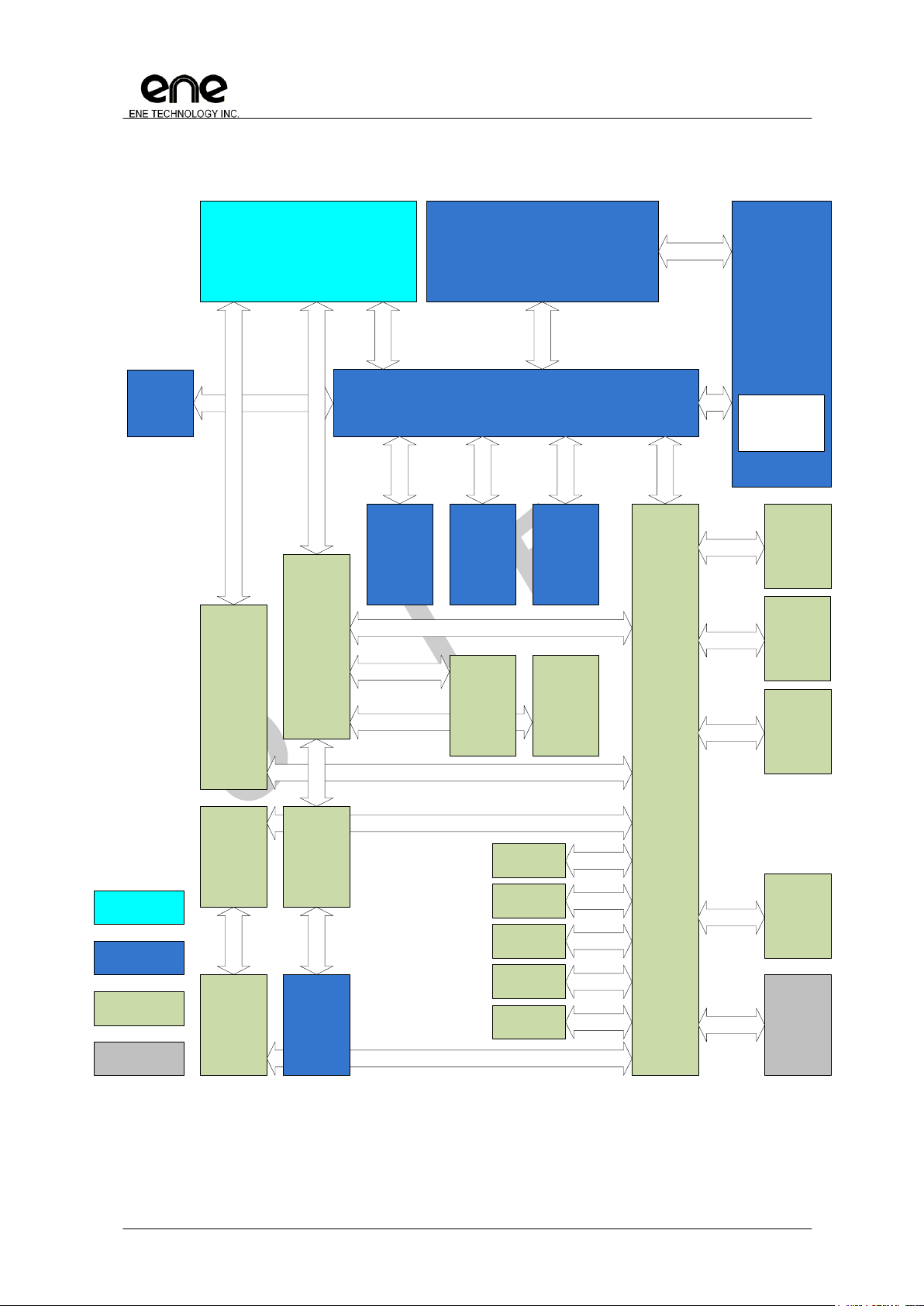
1.3 Comparison (KB930 vs. KB9012)
Copyright© 2011, ENE Technology Inc.
7
KB9012 Keyboard Controller Datasheet
CONFIDENTIAL
LPC I/F
8051
build-in with
2 16-bit timers
1 UART
24 extended interrupt channels
ENE Host BUS
XBI/XIO
ENE
2nd
BUS
4KB
SRAM
GPT
x 4
GPIO
x 106
EC
hardware
command
x 5
KBC
hardware
command
x 8
FAN
X 2
WDT
IKB
18 x 8
hardware
command
x 10
PS2
x 3
LPC/FWH
MEM cycles
EC
Port 80
Index
IO Cycles
KBC
IO Cycles
code
Fetching
Bus
Data
Bus
EC Index mode can accessing
full register space by this path
clock
control
DAC
x 4
16.384 Mhz
32.768 Khz
PMU
ADC
X 8
CIR
SPI I/F
ESB
PECI
OWM
SHDI
PWM
X 6
SMBx2
4 ports
PCI clock
32.768 Mhz
GWG
EDI
1.4 Block Diagram
Copyright© 2011, ENE Technology Inc.

8
KB9012 Keyboard Controller Datasheet
CONFIDENTIAL
2143658
7109
60
59
58
57
56
55
54
53
52
51
50
49
48
47
46
45
44
43
42
41
40
39
38
37
36
35
34
33
KSI1
KSI0
KSO15
KSO14
KSO13
KSO12
KSO11
KSO10
KSO9
KSO8
KSO7
KSO6
KSO5
KSO4
KSO3
KSO2
KSO1
KSO0
CLKRUN#
ECRST#
GPIO1A
GND
GPIO19
VCC
1112131415161718192021222324252627
28
105
106
107
108
109
110
111
112
113
114
115
116
117
118
119
120
121
122
123
124
125
126
127
128
293031
32
64
63
62
61
KSI5
KSI4
KSI3
KSI2
101
102
103
104
97
98
99
100
KB9012
128-LQFP
9695949392
91
90
8981888786
83
82
85
84
75
80
77
76
79
78
69
74
71
70
73
72
65
676668
KSI6
KSI7
AD0
AD1
GA20
KBRST#
SERIRQ
LFRAME#
LAD3
GPIO04
GPIO0A
LAD0
GPIO08
VCC
GPIO07
LAD1
PCIRST#
LAD2
PCICLK
GND
GPIO0D
GPIO0C
GPIO0B
SCI#
PWM0
VCC
PWM1
GND
PWM2
FANPWM0
FANPWM1
FANFB0
FANFB1
GPIO16
GPIO18
GPIO17
AD2
AD3
AVCC
DA0
DA3
DA2
DA1
AGND
AD4
AD5
SCL1
SDA1
KSO17
KSO16
SCL0
SDA0
PSDAT1
PSCLK1
PSDAT2
PSCLK2
PSDAT3
PSCLK3
GPIO50
GPIO52
GPIO53
GPIO54
GPIO55
GND
GPIO56
VCC
GPXIOA00
GPXIOA01
GPXIOA02
GPXIOA03
GPXIOA04
GPXIOA05
GPXIOA06
GPXIOA07
GPXIOA08
GPXIOA09
GPXIOA10
GPXIOA11
GPXIOD00
GPXIOD01
GPXIOD02
GPXIOD03
GPXIOD04
GPXIOD05
GPXIOD06
GPXIOD07
GND_0
VCC_0
GPIO5B
GPIO5C
GPIO57
V18R
VCC
GPIO58
GPIO5A
GPIO59
AD6
AD7
GPIO5D
GPIO5E
2. Pin Assignment and Description
2.1 KB9012 128-pin LQFP Diagram Top View
Copyright© 2011, ENE Technology Inc.

9
KB9012 Keyboard Controller Datasheet
CONFIDENTIAL
A1 A11A10A9A8A7A6A5A4A3A2 A12 A13
B1 B11B10B9B8B7B6B5B4B3B2 B12 B13
C1 C2 C12 C13
D1 D10D9D8D7D6D5D4D2 D12 D13
E1 E10E9E8E7E6E5E4E2 E12 E13
F1 F10F9F5F4F2 F12 F13
G1 G10G9G5G4G2 G12 G13
H1 H10H9H5H4H2 H12 H13
J1 J10J9J8J7J6J5J4J2 J12 J13
K1 K10K9K8K7K6K5K4K2 K12 K13
L1 L2 L12 L13
M1
M11M10
M9M8M7M6M5M4M3M2
M12 M13
N1 N11N10N9N8N7N6N5N4N3N2 N12 N13
GPXIOA01 GPIO55 GPIO54 GPIO52 PSCLK3 SDA1 SDA0 SCL0 DA1 DA2 AGND
AD3 AD1
GPXIOA00 GPIO56 GPIO53 GPIO50 PSDAT3 GPIO40(AD6) GPIO41(AD7) SCL1 DA3 DA0 AVCC
AD2 AD0
GPXIOA02
GPXIOD00
GPXIOA04 GPXIOA05
GPXIOA08 GPXIOA06
GPXIOA11 GPXIOA10
GPXIOD02 GND
GPXIOD04GPXIOD07(PECI)
XCLKI (MOSI)
XCLKO (MISO)
V18R KBRST#
KSI5 KSI6
KSI3 KSI4
KSI1 KSI2
VCC ECRST#
KSO1 KSO0
KSO2 KSO3
KSO9 KSO8
KSO11 KSO10
GPIO1A GPIO08
VCC GPIO19
GPIO18
GND
GPXIOA03 PSDAT2 PSCLK1 AD5 KSO17 KSI0
KSI7
GPXIOA07 PSCLK2 PSDAT1 AD4 KSO16 KSO15
KSO14
GPXIOA09 GPXIOD01
GPXIOD05 GPXIOD03
GPXIOD06 GPIO57
KSO13
KSO12
KSO6
KSO7
KSO5
KSO4
VCC GPIO04 VCC VCC GND GND
GND
LFRAME# LAD1 GPIO0A VCC GPIO11 GPIO17
GPIO16
LAD2 PCIRST# CLKRUN# GPIO0C PWM1 PWM0
FANPWM0
FANFB0
LAD0 PCICLK SCI# GPIO0B GPIO0D GPIO07
FANPWM1
FANFB1
(SPICLK) GA20 SERIRQ
GPIO59 (SPICS#) LAD3
2.2 KB9012 128 LFBGA Ball Map
Copyright© 2011, ENE Technology Inc.

10
KB9012 Keyboard Controller Datasheet
CONFIDENTIAL
KB9012
Pin No.
KB9012
BGA
Name
GPIO
Alt
Output
Alt.
Input
Default
ECRST#
L/H
IO CELL
1
M2
GA20
GPIO00
GA20
GPIO00
HiZ / HiZ
BQC04HIV
2
L2
KBRST#
GPIO01
KBRST#
GPIO01
HiZ / HiZ
BQC04HIV
3
M3
SERIRQ
HiZ / HiZ
BQCZ16HIV
4
K4
LFRAME#
HiZ / HiZ
BQCZ16HIV
5
N3
LAD3
HiZ / HiZ
BQCZ16HIV
6
J5
GPIO04
GPIO04
GPIO04
HiZ / HiZ
BQC04HIV
7
M4
LAD2
HiZ / HiZ
BQCZ16HIV
8
K5
LAD1
HiZ / HiZ
BQCZ16HIV
9
--
VCC VCC
10
N4
LAD0
HiZ / HiZ
BQCZ16HIV
11
--
GND GND
12
N5
PCICLK
HiZ / HiZ
BQCZ16HIV
13
M5
PCIRST#
GPIO05
PCIRST#
GPIO05
IE / IE
BQCZ16HIV
14
N9
GPIO07
GPIO07
i_clk_8051
GPIO07
HiZ / HiZ
BQC04HIV
15
L13
GPIO08
GPIO08
i_clk_peri
GPIO08
HiZ / HiZ
BQC04HIV
16
K6
GPIO0A
GPIO0A
OWM
RLC_RX2
OWM
GPIO0A
HiZ / HiZ
BQC04HIV
17
N7
GPIO0B
GPIO0B
ESB_CLK
GPIO0B
HiZ / HiZ
BQCW16HIV
18
M7
GPIO0C
GPIO0C
ESB_DAT
ESB_DAT
GPIO0C
HiZ / HiZ
BQC08HIV
19
N8
GPIO0D
GPIO0D
RLC_TX2
GPIO0D
HiZ / HiZ
BQC04HIV
20
N6
SCI#
GPIO0E
SCI#
GPIO0E
HiZ / HiZ
BQC04HIV
21
M9
PWM0
GPIO0F
PWM0
GPIO0F
HiZ / HiZ
BQCZ16HIV
22
K7/J7
VCC
VCC
VCC
23
M8
PWM1
GPIO10
PWM1
GPIO10
HiZ / HiZ
BQC04HIV
24
J8/J9/J10
GND
GND
GND
25
K8
GPIO11
GPIO11
PWM2
GPIO11
HiZ / HiZ
BQC04HIV
26
M10
FANPWM0
GPIO12
FANPWM0
GPIO12
HiZ / HiZ
BQC04HIV
27
N10
FANPWM1
GPIO13
FANPWM1
GPIO13
HiZ / HiZ
BQC04HIV
28
M11
FANFB0
GPIO14
FANFB0
GPIO14
HiZ / HiZ
BQC04HIV
29
N11
FANFB1
GPIO15
FANFB1
GPIO15
HiZ / HiZ
BQC04HIV
30
K10
GPIO16
GPIO16
E51TXD
GPIO16
HiZ / HiZ
BQC04HIV
31
K9
GPIO17
GPIO17
E51CLK
E51RXD
GPIO17
HiZ / HiZ
BQC04HIV
32
N12
GPIO18
GPIO18
POWER_FAIL1
GPIO18
HiZ / HiZ
BQC04HIV
2.3 KB9012 Pin Assignment Side A
Copyright© 2011, ENE Technology Inc.

11
KB9012 Keyboard Controller Datasheet
CONFIDENTIAL
KB9012
Pin No.
KB9012
BGA
Name
GPIO
Alt
Output
Alt.
Input
Default
ECRST#
L/H
IO CELL
33
--
VCC VCC
34
M13
GPIO19
GPIO19
PWM3
GPIO19
HiZ / HiZ
BQCZ16HIV
35
--
GND GND
36
L12
GPIO1A
GPIO1A
NUMLED#
GPIO1A
HiZ / HiZ
BQC20HIV
37
K13
ECRST#
IE / IE
BQC04HIV
38
M6
CLKRUN#
GPIO1D
CLKRUN#
CLKRUN#
GPIO1D
HiZ / HiZ
BQCZ16HIV
39
J13
KSO0
GPIO20
KSO0
TP_TEST
GPIO20
IE(PU)/IE(PU)
BQC04HIV
40
J12
KSO1
GPIO21
KSO1
TP_PLL
GPIO21
IE(PU)/IE(PU)
BQC04HIV
41
H12
KSO2
GPIO22
KSO2
TP_TMUX
GPIO22
IE(PU)/IE(PU)
BQC04HIV
42
H13
KSO3
GPIO23
KSO3
TP_PLL_LOCK
GPIO23
IE(PU)/IE(PU)
BQC04HIV
43
H10
KSO4
GPIO24
KSO4
GPIO24
HiZ / HiZ
BQC04HIV
44
H9
KSO5
GPIO25
KSO5
PCICLK
(LPC)
GPIO25
HiZ / HiZ
BQCZ16HIV
45
G9
KSO6
GPIO26
KSO6
PCIRST#
(LPC)
GPIO26
HiZ / HiZ
BQC04HIV
46
G10
KSO7
GPIO27
KSO7
SERIRQ(LPC)
SERIRQ(LPC)
GPIO27
HiZ / HiZ
BQC04HIV
47
G13
KSO8
GPIO28
KSO8
LFRAME#
(LPC)
GPIO28
HiZ / HiZ
BQC04HIV
48
G12
KSO9
GPIO29
KSO9
GPIO29
HiZ / HiZ
BQC04HIV
49
F13
KSO10
GPIO2A
KSO10
GPIO2A
HiZ / HiZ
BQC04HIV
50
F12
KSO11
GPIO2B
KSO11
LAD3(LPC)
LAD3(LPC)
GPIO2B
HiZ / HiZ
BQC04HIV
51
F10
KSO12
GPIO2C
KSO12
LAD2(LPC)
LAD2(LPC)
GPIO2C
HiZ / HiZ
BQC04HIV
52
F9
KSO13
GPIO2D
KSO13
LAD1(LPC)
LAD1(LPC)
GPIO2D
HiZ / HiZ
BQC04HIV
53
E10
KSO14
GPIO2E
KSO14
LAD0(LPC)
LAD0(LPC)
GPIO2E
HiZ / HiZ
BQC04HIV
54
E9
KSO15
GPIO2F
KSO15
(E51_RXD)
GPIO2F
HiZ / HiZ
BQC04HIV
55
D9
KSI0
GPIO30
(E51_TXD)
KSI0
GPIO30
IE(PU)/IE(PU)
BQC04HIV
56
E12
KSI1
GPIO31 KSI1
GPIO31
IE(PU)/IE(PU)
BQC04HIV
57
E13
KSI2
GPIO32 KSI2
GPIO32
IE(PU)/IE(PU)
BQC04HIV
58
D12
KSI3
GPIO33 KSI3
GPIO33
IE(PU)/IE(PU)
BQC04HIV
59
D13
KSI4
GPIO34
KSI4/EDI_CS
GPIO34
IE(PU)/IE(PU)
BQC04HIV
60
C12
KSI5
GPIO35
KSI5/EDI_CLK
GPIO35
IE(PU)/IE(PU)
BQC04HIV
61
C13
KSI6
GPIO36
KSI6/EDI_DIN
GPIO36
IE(PU)/IE(PU)
BQC04HIV
62
D10
KSI7
GPIO37
EDI_DO
KSI7
GPIO37
IE(PU)/IE(PU)
BQC04HIV
63
B13
AD0
GPIO38 AD0
GPIO38
HiZ / HiZ
BQCZT04IV
64
A13
AD1
GPIO39 AD1
GPIO39
HiZ / HiZ
BQCZT04IV
2.4 KB9012 Pin Assignment Side B
Copyright© 2011, ENE Technology Inc.
12
KB9012 Keyboard Controller Datasheet
CONFIDENTIAL
KB9012
Pin No.
KB9012
BGA
Name
GPIO
Alt
Output
Alt.
Input
Default
ECRST#
L/H
IO CELL
65
B12
AD2
GPIO3A
AD2
GPIO3A
HiZ / HiZ
BQCZT04IV
66
A12
AD3
GPIO3B
AD3
GPIO3B
HiZ / HiZ
BQCZT04IV
67
B11
AVCC AVCC
68
B10
DA0
GPIO3C
DA0
GPIO3C
HiZ / HiZ
BQCZT04IV
69
A11
AGND AGND
70
A9
DA1
GPIO3D
DA1
GPIO3D
HiZ / HiZ
BQCZT04IV
71
A10
DA2
GPIO3E
DA2
GPIO3E
HiZ / HiZ
BQCZT04IV
72
B9
DA3
GPIO3F
DA3
GPIO3F
HiZ / HiZ
BQCZT04IV
73
B6
AD6
GPIO40
CIR_RX
/ AD6
GPIO40
HiZ / HiZ
BQCZT04IV
74
B7
AD7
GPIO41
CIR_RLC_TX
AD7
GPIO41
HiZ / HiZ
BQCZT04IV
75
E7
AD4
GPIO42
AD4
GPIO42
HiZ / HiZ
BQCZT04IV
76
D7
AD5
GPIO43
AD5
GPIO43
HiZ / HiZ
BQCZT04IV
77
A8
SCL0
GPIO44
SCL0
GPIO44
HiZ / HiZ
BQC04HI
78
A7
SDA0
GPIO45
SDA0
GPIO45
HiZ / HiZ
BQC04HI
79
B8
SCL1
GPIO46
SCL1
GPIO46
HiZ / HiZ
BQC04HI
80
A6
SDA1
GPIO47
SDA1
GPIO47
HiZ / HiZ
BQC04HI
81
E8
KSO16
GPIO48
KSO16
GPIO48
HiZ / HiZ
BQC04HIV
82
D8
KSO17
GPIO49
KSO17
GPIO49
HiZ / HiZ
BQC04HIV
83
D6
PSCLK1
GPIO4A
PSCLK1 / SCL2
GPIO4A
HiZ / HiZ
BQC04HI
84
E6
PSDAT1
GPIO4B
PSDAT1 / SDA2
GPIO4B
HiZ / HiZ
BQC04HI
85
E5
PSCLK2
GPIO4C
PSCLK2
/ SCL3
GPIO4C
HiZ / HiZ
BQCZ16HIV
86
D5
PSDAT2
GPIO4D
PSDAT2
/ SDA3
GPIO4D
HiZ / HiZ
BQC20HIV
87
A5
PSCLK3
GPIO4E
PSCLK3
GPIO4E
HiZ / HiZ
BQC04HI
88
B5
PSDAT3
GPIO4F
PSDAT3
GPIO4F
HiZ / HiZ
BQC04HI
89
B4
GPIO50
GPIO50
GPIO50
HiZ / HiZ
BQC04HI
90
A4
GPIO52
GPIO52
E51CS#
GPIO52
HiZ / HiZ
BQC20HIV
91
B3
GPIO53
GPIO53
CAPSLED#
E51TMR1
GPIO53
HiZ / HiZ
BQC20HIV
92
A3
GPIO54
GPIO54
WDT_LED#
E51TMR0
GPIO54
HiZ / HiZ
BQC20HIV
93
A2
GPIO55
GPIO55
SCROLED#
E51INT0
GPIO55
HiZ / HiZ
BQC20HIV
94
--
GND GND
95
B2
GPIO56
GPIO56
E51INT1
GPIO56
HiZ / HiZ
BQC04HIV
96
--
VCC VCC
2.5 KB9012 Pin Assignment Side C
Copyright© 2011, ENE Technology Inc.
13
KB9012 Keyboard Controller Datasheet
CONFIDENTIAL
KB9012
Pin No.
KB9012
BGA
Name
GPIO
Alt
Output
Alt.
Input
Default
ECRST#
L/H
IO CELL
97
B1
GPXIOA00
GPXIOA00
SHICS#
SDICS#
HiZ / HiZ
BQC04HIV
98
A1
GPXIOA01
GPXIOA01
SHICLK
SDICLK
HiZ / HiZ
BQC04HIV
99
C1
GPXIOA02
GPXIOA02
SHIDO
SDIDI
HiZ / HiZ
BQC04HIV
100
D4
GPXIOA03
GPXIOA03
POWER_FAIL0
FANFB2
HiZ / HiZ
BQC04HIV
101
D1
GPXIOA04
GPXIOA04
FANFB3
HiZ / HiZ
BQC04HIV
102
D2
GPXIOA05
GPXIOA05
VCIN1
HiZ / HiZ
BQC04HIV
103
E2
GPXIOA06
GPXIOA06
VCOUT1
HiZ / HiZ
BQC04HIV
104
E4
GPXIOA07
GPXIOA07
VCOUT0
HiZ / HiZ
BQC04HIV
105
E1
GPXIOA08
GPXIOA08
HiZ / HiZ
BQCZ16HIV
106
F4
GPXIOA09
GPXIOA09
HiZ / HiZ
BQCZ16HIV
107
F2
GPXIOA10
GPXIOA10
HiZ / HiZ
BQCZ16HIV
108
F1
GPXIOA11
GPXIOA11
GWG
HiZ / HiZ
BQCZ16HIV
109
C2
GPXIOD00
GPXIOD00
SDIDO
SHIDI /
VCIN0
HiZ / HiZ
BQC04HIV
110
F5
GPXIOD01
GPXIOD01
AC_IN
HiZ / HiZ
BQC04HIV
111
J6
VCC_0
HiZ / HiZ
VCC_0
112
G1
GPXIOD02
GPXIOD02
ALW_PWR_EN
HiZ / HiZ
BQC04HIV
113
G2
GND_0
HiZ / HiZ
GND_0
114
G5
GPXIOD03
GPXIOD03
ON/OFFBTN#
HiZ / HiZ
BQC04HIV
115
H1
GPXIOD04
GPXIOD04
HiZ / HiZ
BQC04HIV
116
G4
GPXIOD05
GPXIOD05
HiZ / HiZ
BQC04HIV
117
H4
GPXIOD06
GPXIOD06
HiZ / HiZ
BQC04HIV
118
H2
GPXIOD07
GPXIOD07
PECI
PECI
HiZ / HiZ
BQC04HIVPECI
119
K2
GPIO5B
GPIO5B
(MISO)
GPIO5B
HiZ / HiZ
BQCZ16HIV
120
J2
GPIO5C
GPIO5C
(MOSI)
GPIO5C
HiZ / HiZ
BQCZ16HIV
121
H5
GPIO57
GPIO57
XCLK32K
GPIO57
HiZ / HiZ
BQC04HIV
122
J1
GPIO5D
GPIO5D
(XCLKI)
GPIO5D
HiZ / HiZ
BQCZT04IV
123
K1
GPIO5E
GPIO5E
(XCLKO)
GPIO5E
HiZ / HiZ
BQCZT04IV
124
L1
V18R
125
J4
VCC VCC
126
M1
GPIO58
GPIO58
(SPICLK)
GPIO58
HiZ / HiZ
BQCW16HIV
127
N1
GPIO59
GPIO59
GPIO59
IE / IE
BQC04HIV
128
N2
GPIO5A
GPIO5A
(SPICS#)
GPIO5A
HiZ / HiZ
BQCZ16HIV
2.6 KB9012 Pin Assignment Side D
* Please note, crystal pad signal frequency should be lower than 1MHz.
Copyright© 2011, ENE Technology Inc.
14
KB9012 Keyboard Controller Datasheet
CONFIDENTIAL
Cell
Description
Application
BQCZ16HIV
Schmitt trigger, 16mA Output / Sink Current, Input / Output / Pull Up
Enable(40KΩ ), 5 V Tolerance.
GPIO, LPC
I/F
BQC04HIV
Schmitt trigger, 4mA Output / Sink Current, Input / Output / Pull Up
Enable(40KΩ ), 5 V Tolerance
GPIO
BQCW16HIV
Schmitt trigger, 16mA Output / Sink Current, 5 V Tolerance, Input / Output / Pull
Up Enable
ESB_CLK/
SPI_CLK
BQC04HI
Schmitt trigger, 4mA Output / Sink Current, 5 V Tolerance, Input / Output
Enable
GPIO
BQC08HIV
Schmitt trigger, 8mA Output / Sink Current, 5V Tolerance, Input / Output / Pull
Up Enable
ESB_DAT
BQC04HIVPECI
Mixed Mode IO, PECI enable, with GPIO
GPIO: Schmitt trigger, 4mA Output / Sink Current,
PECI: 0.9V~1.2V
PECI, GPIO
BQCZT04IV
***
Mixed Mode IO, AE enable, with GPIO
GPIO: Schmitt trigger, 4mA Output / Sink Current, Input / Output / Pull Up
Enable
ADC/DAC,
XCLKI,
XCLKO
Cell
Output
Input
Analog
Signal
Pull-High
Enable(40k)
5V
Tolerance
Current
(mA)
Application
BQCZ16HIV
ˇ ˇ ˇ ˇ
8~16
GPIO, LPC
I/F
BQC04HIV
ˇ ˇ ˇ ˇ
2~4
GPIO
BQCW16HIV
ˇ ˇ ˇ ˇ
8~16
ESB_CLK/
SPI_CLK
BQC04HI
ˇ ˇ ˇ
2~4
GPIO
BQC08HIV
ˇ ˇ ˇ ˇ
4~8
ESB_DAT
BQC04HIVPECI
ˇ ˇ ˇ ˇ
2~4
PECI, GPIO
BQCZT04IV
ˇ
ˇ ˇ ˇ
2~4
ADC/DAC,
XCLKI,
XCLKO
2.7 I/O Cell Descriptions
2.7.1 I/O Buffer Table
** Please note, the total current in each side on VCC or VSS of chip can not exceed over 48mA.
*** Please note, As BQCZT04IV with shared crystal pad, signal frequency should be lower than 1MHz.
2.7.2 I/O Buffer Characteristic Table
* 5V Tolerance, only if pull-high disable and output disable.
Copyright© 2011, ENE Technology Inc.
15
KB9012 Keyboard Controller Datasheet
CONFIDENTIAL
Trap Name
Pin No.
Description
TP_TEST
(GPIO20,KSO0)
39
While this trap is asserted to be low, the internal DPLL circuit uses other clock source
for reference, instead of 32KHz oscillator.
Low: test clock mode enable
High: normal mode using 32KHz oscillator.
TP_PLL
(GPIO21,KSO1)
40
While this trap is asserted to be low, some DPLL related signals can be output for
test.
Low: DPLL test mode enable.
High: DPLL test mode disable
TP_TMUX
(GPIO22,KSO2)
41
TestMux Mode Trap
Low: Test mode
High: Normal operation
TP_PLL_Lock
(GPIO23,KSO3)
42
This trap is used for eFlash & EDI operation, , the 8051 will be held at reset state
LOW: Test Mode
HIGH: Normal operation
* Please note while TP_TMUX and TP_PLL_Lock keep low at the same time, a mechanism called FlashDirectAccess will
enable. That is, users can flush and program a SPI flash via specific IKB pins with external tool.
FlashDirectAccess:
The KBC provides a new interface to program SPI flash via IKB interface. With this feature, users can easily utilize 4 pins
from keyboard matrix (IKB) without disassembly whole machine. These 4 pins are connected directly to external SPI-Flash
interface. The following table shows the mapped pins while entering FlashDirectAccess mode.
EDI : For detail ENE Debug Interface, please refer the EDI section for enabling, instruction, and application.
Pin No.
Normal Mode
FlashDirectAccess Mode
59
KSI4 (I)
(Input) EDI_CS, Transfer signal from terminal into KBC and though SPICS# to SPI_Flash
60
KSI5 (I)
(Input) EDI_CLK, Transfer signal from terminal into KBC and though SPICLK to SPI_Flash
61
KSI6 (I)
(Input) EDI_DIN, Transfer signal from terminal into KBC and though MOSI to SPI_Flash
62
KSI7 (I)
(Output) EDI_DO, Transfer signal from terminal into KBC and though MISO to SPI_Flash
ENE
KBC
Terminal
SPI-Flash
P128, SPICS#
P120, MOSI
P119, MISO
P126, SPICLK
P59, KSI4
P60, KSI5
P61, KSI6
P62, KSI7
EDI_CS
EDI_CLK
EDI_DIN
EDI_DO
3. Pin Descriptions
3.1 Hardware Trap
Hardware trap pins are used to latch external signal at rising edge of ECRST#. The hardware
trap pins are for some special purpose which should be defined while boot-up. The following table
gives the collection of hardware trap pins. Please note, all the following hardware trap pins are
pull-high internally after reset.
Copyright© 2011, ENE Technology Inc.
16
KB9012 Keyboard Controller Datasheet
CONFIDENTIAL
Pin Name
Pin No.
Direction
Description
LAD[3:0]
5, 7,8,10
I/O
LPC address bus.
LFARAME#
4
I
LPC frame control signal.
PCIRST#
13
I
LPC module reset by this signal.
PCICLK
12
I
33MHz PCI clock input.
SERIRQ
3
I/O
Serial IRQ
CLKRUN#
38
I/OD
Clock run control
Pin Name
Pin No.
Direction
Description
PSCLK1
83
I/OD
PS/2 port 1 clock
Muxed with SMBus port 2 clock
PSDAT1
84
I/OD
PS/2 port 1 data
Muxed with SMBus port 2 data
PSCLK2
85
I/OD
PS/2 port 2 clock
Muxed with SMBus port 3 clock
PSDAT2
86
I/OD
PS/2 port 2 data
Muxed with SMBus port 3 data
PSCLK3
87
I/OD
PS/2 port 3 clock
PSDAT3
88
I/OD
PS/2 port 3 data
Pin Name
Pin No.
Direction
Description
KSO[17:0]
82,81,54-39
O
Keyboard Scan Out
KSI[7:0]
62-55
I
Keyboard Scan In
Pin Name
Pin No.
Direction
Description
SCL0
77
I/OD
SMBus clock (interface 0)
SDA0
78
I/OD
SMBus data (interface 0)
SCL1
79
I/OD
SMBus clock (interface 1)
SDA1
80
I/OD
SMBus data (interface 1)
SCL2
83
I/OD
SMBus clock (interface 2)
Muxed with PS/2 port 1 clock
SDA2
84
I/OD
SMBus data (interface 2)
Muxed with PS/2 port 1 data
SCL3
85
I/OD
SMBus clock (interface 3)
Muxed with PS/2 port 2 clock
SDA3
86
I/OD
SMBus data (interface 3)
Muxed with PS/2 port 2 data
3.2 Pin Descriptions by Functions
3.2.1 Low Pin Count I/F Descriptions.
3.2.2 PS/2 I/F Descriptions
3.2.3 Internal Keyboard Encoder (IKB) Descriptions
3.2.4 SMBus Descriptions
Copyright© 2011, ENE Technology Inc.
17
KB9012 Keyboard Controller Datasheet
CONFIDENTIAL
Pin Name
Pin No.
Direction
Description
FANPWM0
26
O
FANPWM0 output
FANPWM1
27
O
FANPWM1 output
FANFB0
28
I
FAN0 tachometer input
FANFB1
29
I
FAN1 tachometer input
FANFB2
100
I
FAN2 tachometer input
FANFB3
101
I
FAN3 tachometer input
Pin Name
Pin No.
Direction
Description
PWM0
21
O
PWM pulse output
PWM1
23
O
PWM pulse output
PWM2
25
O
PWM pulse output
PWM3
34
O
PWM pulse output
Pin Name
Pin No.
Direction
Description
AD[3:0]
66-63
I
10bit A/D converter input
AD[5:4]
76,75
I
10bit A/D converter input
AD6
73
I
10bit A/D converter input
AD7
74
I
10bit A/D converter input
Pin Name
Pin No.
Direction
Description
DA[3:0]
72-70,68
O
8bit D/A converter output
Pin Name
Pin No.
Direction
Description
E51TXD
30
O
8051 serial port, transmit port.
E51RXD
31
I
8051 serial port, receive port.
E51CLK
31
O
For different serial scheme, E51CLK will shift out clock.
E51CS#
90
O
E51TMR0
92
I
E51INT0
93
I
E51TMR1
91
I
E51INT1
95
I
3.2.5 FAN Descriptions
3.2.6 Pulse Width Modulation (PWM) Descriptions
3.2.7 Analog-to-Digital Converter Descriptions
3.2.8 Digital-to-Analog Converter Descriptions
3.2.9 8051 External I/F Descriptions
Copyright© 2011, ENE Technology Inc.
18
KB9012 Keyboard Controller Datasheet
CONFIDENTIAL
Pin Name
Pin No.
Direction
Description
XCLKI
122
I
32.768KHz input
XCLKO
123
O
32.768KHz output
Pin Name
Pin No.
Direction
Description
GA20 1 O
KBC will gate A20 address line
KBRST#
2
O
KBRST# is used to generate system reset.
SCI#
20
O
SCI# asserts to the system for requesting service while
related events occur.
ECRST#
37
I
While ECRST# asserted, the KBC will reset globally.
OWM
16
I/O
One Wire Master input and output signal
PECI
118
I/O
PECI input and output signal
GWG
108
O
General Waveform Generator for 3D application
POWER_FAIL0
100
O
Used to indicate the power fail under Power Fail Voltage.
POWER_FAIL1
32
O
Used to indicate the power fail under Power Fail Voltage.
Pin Name
Pin No.
Direction
Description
VCIN0
109
I
Voltage comparator input port0
VCOUT0
104
O
Voltage comparator output port0
VCIN1
102
I
Voltage comparator input port1
VCOUT1
103
O
Voltage comparator output port1
Pin Name
Pin No.
Direction
Description
VCC
9,22,33,96,111,125
Power supply for digital plane.
GND
11,24,35,94,113
Power ground for digital plane.
AVCC
67
Power supply for analog plane.
AGND
69
Power ground for analog plane.
V18R
124
Connected to external Capacitor for internal 1.8V
VCC_0
111
Power supply for 51ON power management
GND_0
113
Power ground for 51ON power management
3.2.10 External Clock Descriptions
(These pins are reserved for external CLK design structure, also could be set as GPIO function)
3.2.11 Miscellaneous Signals Descriptions
3.2.12 Voltage Comparator Pins Descriptions
3.2.13 Power Pins Descriptions
Copyright© 2011, ENE Technology Inc.

19
KB9012 Keyboard Controller Datasheet
CONFIDENTIAL
Pin Name
Pin No.
Direction
Description
GPXIOD01
110
I/O
AC_IN
GPXIOD02
112
I/O
ALW_PWR_EN
GPXIOD03
114
I/O
ON/OFFBTN#
3.2.14 51ON Power Pins Descriptions
(The 51ON power management are with different power domain from main IC power)
Copyright© 2011, ENE Technology Inc.
20
KB9012 Keyboard Controller Datasheet
CONFIDENTIAL
Power Plane
Description
Power
Ground
Digital Plane
This power provides power for all digital logic no matter what
power mode is.
VCC
GND
Analog Plane
This power provides power for all analog logic, such as A/D
and D/A converter.
AVCC
AGND
Digital V1.8
The system inputs 3.3V power and the internal regulator
outputs 1.8V voltage. The 1.8V output should connect a
capacitor for stable purpose.
V1.8
GND
Power Latch
Plane
This power provides power for the power-latch circuit. It could
help to provide power saving management.
VCC_0
GND_0
4. Module Descriptions
4.1 Chip Architecture
4.1.1 Power Planes
Power planes are ±10% tolerance for recommend operation condition, The KBC provides
V1.8 power plane for different generation.
Copyright© 2011, ENE Technology Inc.

21
KB9012 Keyboard Controller Datasheet
CONFIDENTIAL
Clock
Description
PCICLK
PCI clock 33MHz for LPC I/F.
DPLL_CLK
Main clock for 8051/peripheral. DPLL clock can be generated with or without XCLK for
reference. DPLL clock can be divided for different applications. Fig. 4-1 gives an example for
illustration.
XCLKI
External 32.768KHz for reference.
SPI Clock (X)
Main Clock (Y)
Peripheral Clock (Z)
CLKCFG[6]=0
(default)
CLKCFG[6]=1
CLKCFG[6]=0
(default)
CLKCFG[6]=1
CLKCFG[6]=0
(default)
CLKCFG[6]=1
CLKCFG[3:2]=0
(default)
16*
66
8* 8 4*
4
CLKCFG[3:2]=1
32
66
16
16 8 8
CLKCFG[3:2]=2
32
66
22
22
11
11
CLKCFG[3:2]=3
32
66
32
32
16
16
* While power on default, no matter what value CLKCFG[3:2], CLKCFG[6] are, the dividend (X,Y,Z) is always (4,
8, 16). The PCI clock is 66MHz, X= 66/4 = 16MHz, Y= 66/8 = 8Mhz , Z= 66/16 = 4MHz
Be noted that, these clock frequency is only valid after KBC correctly referring clock.
4.1.2 Clock Domains
Three clock sources, PCICLK, DPLL_CLK and XCLKI will be discussed in this section. A
summary is list in the following table.
The following figure shows more detail about the operation in the KBC. The external
32.768KHz is provided for two purposes. One is to provide an accurate reference for internal DPLL
module, and the other one is to provide another clock source for watchdog timer.
The possible (X,Y,Z) combination with exact clock value is summarized as the following table.
Copyright© 2011, ENE Technology Inc.

22
KB9012 Keyboard Controller Datasheet
CONFIDENTIAL
PCICLK
0xFF1F[5]
PLLCFG2
0
1
External Source
0xFE8A[0]
Internal OSC
0xFE8A[1]
0xFE8A[2]
CLK32CR
0
1
10-bit
Divider
DPLL
& Clock
Generator
0xFF1F[4]
PLLCFG2
0
1
WDT
0
1
0xFE80[7]
WDTCFG
{
XBI, SPI Flash
8051, SRAM, GPT, GPIO
Peripheral
0xFF0D[5]
CLKCFG
Enable
0xFE8A[5:4]
CLK32CR
Pin 122 , Pin 123
00 : GPIO5D, GPIO5E
01 : GPIO5D, XCLKO as external clock input
10 : XLCKI, GPIO5E, where XLCKI is external clock input
11 : XLCKI, XCLKO, as crystal pads to external crystal
KBC
Pin 122
Pin 123
32k Source Pad Configuration
Note: Internal OSC of KB9012 application
Since KB9012 also provide internal OSC, the clock source selection is similar
to KBx930. Developer could choose clock source from internal-OSC, external
crystal, or host LPCLCK depending on different application and system status. As
following is simplified clocking distribution tree for setting.
Please note that, KB9012 also support external clock source without crystal
device. For correctly configuration, please contact your sales or technical
representative for the application note: Using External OSC Clock Source for ENE Keyboard
Controller.
Copyright© 2011, ENE Technology Inc.

23
KB9012 Keyboard Controller Datasheet
CONFIDENTIAL
4.1.3 PCICLK and CLKRUN#
While system power-on, the host starts to drive CLKRUN# low for a while to inform the slaves
that a 33MHz PCICLK will be given. At this moment, CLKRUN# of KBC is in input mode. If the host
tries to stop the PCICLK for some purpose, the CLKRUN# will be de-asserted. In KB9012 design,
the KBC responses CLKRUN# signal according to LPC_CDCSR configuration. Please refer section
4.13.7 LPC Registers Description for KB9012 application. For more detail please refer to PCI Mobile
Design Guide version 1.1.
Copyright© 2011, ENE Technology Inc.

24
KB9012 Keyboard Controller Datasheet
CONFIDENTIAL
No
Module
Descriptions
Address Range
Size (Byte)
1
Flash
Space mapped to system BIOS
0x0000~0xEBFF
59K
2
XRAM
Embedded SRAM
0xEC00~0xFBFF
4K
3
GPIO
General purpose I/O
0xFC00~0xFC7F
128
1K
4
KBC
Keyboard controller
0xFC80~0xFC8F
16
5
ESB
ENE serial bus controller
0xFC90~0xFC9F
16
6
IKB
Internal keyboard matrix
0xFCA0~0xFCAF
16
7
(ESB)
(Available for ESB)
0xFCB0~0xFCBF
16
8
(ESB)
(Available for ESB)
0xFCC0~0xFCCF
16
9
PECI
PECI controller
0xFCD0~0xFCDF
16
10
RSV
Reserved
0xFCE0~0xFCEF
16
11
OWM
One Wire Master
0xFCF0~0xFCFF
16
12
(ESB)
(Available for ESB)
0xFD00~0xFDFF
256
13
PWM
Pulse width modulation
0xFE00~0xFE1F
32
14
FAN
Fan controller
0xFE20~0xFE4F
48
15
GPT
General purpose timer
0xFE50~0xFE6F
32
16
SDIH/
SDID
SPI host interface/
SPI device interface
0xFE70~0xFE7F
16
17
WDT
Watchdog timer
0xFE80~0xFE8F
16
18
LPC
Low pin count interface
0xFE90~0xFE9F
16
19
XBI
X-bus interface
0xFEA0~0xFEBF
32
20
CIR
Consumer IR controller
0xFEC0~0xFECF
16
21
GWG
General Waveform Generation
0xFED0~0xFEDF
16
22
PS2
PS/2 interface
0xFEE0~0xFEFF
32
23
EC
Embedded controller
0xFF00~0xFF2F
48
24
GPWU
General purpose wakeup event
0xFF30~0xFF7F
80
25
RSV
Reserved
0xFF80~0xFF8F
16
26
SMBus
SMBus controller 0
0xFF90~0xFFBF
48
27
RSV
Reserved
0xFFC0~0xFFCF
16
28
SMBus
SMBus controller 1
0xFFD0~0xFFFF
48
4.1.4 Internal Memory Map
Copyright© 2011, ENE Technology Inc.

25
KB9012 Keyboard Controller Datasheet
CONFIDENTIAL
GPIO
Alt. Output
Alt. Input
Default Alt. Output
Alt. Selection Reg.
GPIO00
GA20
GPIO00
GPIOFS00.[0]
GPIO01
KBRST#
GPIO01
GPIOFS00.[1]
GPIO02*
GPIO02
GPIOFS00.[2]
GPIO03*
GPIO03
GPIOFS00.[3]
GPIO04
GPIO04
GPIOFS00.[4]
GPIO05
PCIRST#
GPIO05
GPIOFS00.[5]
GPIO06*
GPIO06
GPIOFS00.[6]
GPIO07
i_clk_8051
GPIO07
GPIOFS00.[7]
GPIO08
i_clk_peri
GPIO08
GPIOFS08.[0]
GPIO09*
GPIO09
GPIOFS08.[1]
GPIO0A
OWM
RLC_RX2
/ OWM
GPIO0A
GPIOFS08.[2]
OWMCFG[7]
GPIO0B
ESB_CLK
GPIO0B
GPIOFS08.[3]
GPIO0C
ESB_DAT
ESB_DAT
GPIO0C
GPIOFS08.[4]
GPIO0D
RLC_TX2
GPIO0D
GPIOFS08.[5]
GPIO0E
SCI#
GPIO0E
GPIOFS08.[6]
GPIO0F
PWM0
GPIO0F
GPIOFS08.[7]
GPIO10
PWM1
GPIO10
GPIOFS10.[0]
GPIO11
PWM2
GPIO11
GPIOFS10.[1]
GPIO12
FANPWM0
GPIO12
GPIOFS10.[2]
GPIO13
FANPWM1
GPIO13
GPIOFS10.[3]
GPIO14
FANFB0
GPIO14
GPIOFS10.[4]
GPIO15
FANFB1
GPIO15
GPIOFS10.[5]
GPIO16
E51TXD
GPIO16
GPIOFS10.[6]
GPIO17
E51CLK
E51RXD
GPIO17
GPIOFS10.[7]
GPIO18
POWER_FAIL1
GPIO18
GPIOFS18.[0]
GPIO19
PWM3
GPIO19
GPIOFS18.[1]
GPIO1A
NUMLED#
GPIO1A
GPIOFS18.[2]
GPIO1B*
GPIO1B
GPIOFS18.[3]
GPIO1C*
GPIO1C
GPIOFS18.[4]
4.2 GPIO
GPIOFSx is only for Output Function Selection, not for Input Function.
Example1 – GPIO14 is used as FANFB1, then
GPIO(GPIOFS10) 0xFC02 b‘4 must be 0,
GPIO(GPIOIE10) 0xFC62 b‘4 must be 1.
Example2 – PS/2 clock/data lines and SMBus clock/data are bi-directional.
They must be programmed as Output Function Selection = 1 and Input Enable = 1.
For other specific GPIO initialization, please refer the SW programming guide.
4.2.1 GPIO Function Description The GPIO module is flexible for different applications. Each GPIO pin can be configured
as alternative input or alternative output mode. The alternative function can be selected by register
setting. A summary table is given as below for more detail.
Copyright© 2011, ENE Technology Inc.

26
KB9012 Keyboard Controller Datasheet
CONFIDENTIAL
GPIO
Alt. Output
Alt. Input
Default Alt. Output
Alt. Selection Reg.
GPIO1D
CLKRUN#
CLKRUN#
GPIO1D
GPIOFS18.[5]
GPIO1E*
GPIO1E
GPIOFS18.[6]
GPIO1F*
GPIO1F
GPIOFS18.[7]
GPIO20
KSO00
TP_TEST
GPIO20
GPIOFS20.[0]
GPIO21
KSO01
TP_PLL
GPIO21
GPIOFS20.[1]
GPIO22
KSO02
TP_TMUX
GPIO22
GPIOFS20.[2]
GPIO23
KSO03
TP_PLL_Lock
GPIO23
GPIOFS20.[3]
GPIO24
KSO04
GPIO24
GPIOFS20.[4]
GPIO25
KSO05
PCICLK (LPC)
GPIO25
GPIOFS20.[5]
GPIO_MISC2[7]
GPIO26
KSO06
PCIRST# (LPC)
GPIO26
GPIOFS20.[6]
GPIO_MISC2[7]
GPIO27
KSO07
SERIRQ (LPC)
SERIRQ (LPC)
GPIO27
GPIOFS20.[7]
GPIO_MISC2[7]
GPIO28
KSO08
LFRAME# (LPC)
GPIO28
GPIOFS28.[0]
GPIO_MISC2[7]
GPIO29
KSO09
GPIO29
GPIOFS28.[1]
GPIO2A
KSO10
GPIO2A
GPIOFS28.[2]
GPIO2B
KSO11
LAD0 (LPC)
LAD0 (LPC)
GPIO2B
GPIOFS28.[3]
GPIO_MISC2[7]
GPIO2C
KSO12
LAD1 (LPC)
LAD1 (LPC)
GPIO2C
GPIOFS28.[4]
GPIO_MISC2[7]
GPIO2D
KSO13
LAD2 (LPC)
LAD2 (LPC)
GPIO2D
GPIOFS28.[5]
GPIO_MISC2[7]
GPIO2E
KSO14
LAD3 (LPC)
LAD3 (LPC)
GPIO2E
GPIOFS28.[6]
GPIO_MISC2[7]
GPIO2F
KSO15
(E51_RXD)
GPIO2F
GPIOFS28.[7]
GPIO_MISC2[2]
GPIO30
(E51_TXD)
KSI0
GPIO30
GPIOFS30.[0]
GPIO_MISC2[2]
GPIO31
KSI1
GPIO31
GPIOFS30.[1]
GPIO32
KSI2
GPIO32
GPIOFS30.[2]
GPIO33
KSI3
GPIO33
GPIOFS30.[3]
GPIO34
KSI4
/ EDI_CS
GPIO34
GPIOFS30.[4]
GPIO35
KSI5
/ EDI_CLK
GPIO35
GPIOFS30.[5]
GPIO36
KSI6
/ EDI_DIN
GPIO36
GPIOFS30.[6]
GPIO37
EDI_DO
KSI7
GPIO37
GPIOFS30.[7]
GPIO38
AD0
GPIO38
GPIOFS38.[0]
GPIO39
AD1
GPIO39
GPIOFS38.[1]
GPIO3A
AD2
GPIO3A
GPIOFS38.[2]
GPIO3B
AD3
GPIO3B
GPIOFS38.[3]
GPIO3C
DA0
GPIO3C
GPIOFS38.[4] ★
Copyright© 2011, ENE Technology Inc.

27
KB9012 Keyboard Controller Datasheet
CONFIDENTIAL
GPIO
Alt. Output
Alt. Input
Default Alt. Output
Alt. Selection Reg.
GPIO3D
DA1
GPIO3D
GPIOFS38.[5] ★
GPIO3E
DA2
GPIO3E
GPIOFS38.[6] ★
GPIO3F
DA3
GPIO3F
GPIOFS38.[7] ★
GPIO40
AD6
CIR_RX
GPIO40
GPIOFS40.[0]
GPIO41
CIR_RLC_TX
AD7
GPIO41
GPIOFS40.[1]
GPIO42
AD4
GPIO42
GPIOFS40.[2]
GPIO43
AD5
GPIO43
GPIOFS40.[3]
GPIO44
SCL0
GPIO44
GPIOFS40.[4]
GPIO45
SDA0
GPIO45
GPIOFS40.[5]
GPIO46
SCL1
GPIO46
GPIOFS40.[6]
GPIO47
SDA1
GPIO47
GPIOFS40.[7]
GPIO48
KSO16
GPIO48
GPIOFS48.[0]
GPIO49
KSO17
GPIO49
GPIOFS48.[1]
GPIO4A
PSCLK1 / SCL2
GPIO4A
GPIOFS48.[2]
GPIO_MISC2[4]
GPIO4B
PSDAT1
/ SDA2
GPIO4B
GPIOFS48.[3]
GPIO_MISC2[4]
GPIO4C
PSCLK2
/ SCL3
GPIO4C
GPIOFS48.[4]
GPIO_MISC2[5]
GPIO4D
PSDAT2
/ SDA3
GPIO4D
GPIOFS48.[5]
GPIO_MISC2[5]
GPIO4E
PSCLK3
GPIO4E
GPIOFS48.[6]
GPIO4F
PSDAT3
GPIO4F
GPIOFS48.[7]
GPIO50
GPIO50
GPIOFS50.[0]
GPIO51*
GPIO51
GPIOFS50.[1]
GPIO52
E51CS#
GPIO52
GPIOFS50.[2]
GPIO53
CAPSLED#
E51TMR1
GPIO53
GPIOFS50.[3]
GPIO54
WDT_LED#
E51TMR0
GPIO54
GPIOFS50.[4]
GPIO55
SCORLED#
E51INT0
GPIO55
GPIOFS50.[5]
GPIO56
E51INT1
GPIO56
GPIOFS50.[6]
GPIO57
XCLK32K
GPIO57
GPIOFS50.[7]
GPIO58
(SPICLK)
GPIO58
GPIO_MISC.[1]
GPIO59
TEST_CLK
GPIO59
GPIOFS58.[1]
GPIO5A
(SPICS#)
GPIO5A
GPIO_MISC.[1]
GPIO5B
(MISO)
GPIO5B
GPIO_MISC.[1]
GPIO5C
(MOSI)
GPIO5C
GPIO_MISC.[1]
GPIO5D
(XCLKI)
GPIO5D
CLK32CR[5:4]
GPIO5E
(XCLKO)
GPIO5E
CLK32CR[5:4]
GPXIOA00
SHICS#
SDICS#
GPXIOA00
GPIO_MISC.[2]
GPXIOA01
SHICLK
SDICLK
GPXIOA01
GPIO_MISC.[2]
GPXIOA02
SHIDO
SDIDI
GPXIOA02
GPIO_MISC.[2]
GPXIOA03
POWER_FAIL0
FANFB2
GPXIOA03
GPXAFS00[3]
FANTMCFG0[0]
Copyright© 2011, ENE Technology Inc.

28
KB9012 Keyboard Controller Datasheet
CONFIDENTIAL
GPIO
Alt. Output
Alt. Input
Default Alt. Output
Alt. Selection Reg.
GPXIOA04
FANFB3
GPXIOA04
GPXAFS00[4]
FANTMCFG1[0]
GPXIOA05
VCIN1
GPXIOA05
VCCR[1]
GPXIOA06
VCOUT1
GPXIOA06
GPXAFS00[6]
GPXIOA07
VCOUT0
GPXIOA07
GPXAFS00[7]
GPXIOA08
GPXIOA08
GPXAFS08[0]
GPXIOA09
GPXIOA09
GPXAFS08[1]
GPXIOA10
GPXIOA10
GPXAFS08[2]
GPXIOA11
GWG
GPXIOA11
GPXAFS08[3]
GPXIOD00
SDIDO
SHIDI / VCIN0
GPXIOD00
GPIO_MISC.[2]
VCCR[0]
GPXIOD01
AC_IN
GPXIOD01
GPXDFS00[1]
GPXIOD02
ALW_PWR_EN
GPXIOD02
GPXDFS00[2]
GPXIOD03
ON/OFFBTN#
GPXIOD03
GPXDFS00[3]
GPXIOD04
GPXIOD04
GPXDFS00[4]
GPXIOD05
GPXIOD05
GPXDFS00[5]
GPXIOD06
GPXIOD06
GPXDFS00[6]
GPXIOD07
PECI
PECI
GPXIOD07
GPXDFS00[7]
* In KB9012, these GPIO pins no more exist. The corresponding register bits do not work.
** Please Note in KB9012, the GPXIOAx / GPXIODx could be configured PU / OD pin by pin.
*** Please note, crystal pad signal frequency should be lower than 1MHz.
★ If DAC function selected, please do not set this register bit.
Copyright© 2011, ENE Technology Inc.

29
KB9012 Keyboard Controller Datasheet
CONFIDENTIAL
4.2.2 GPIO Structures
In this section, the GPIO structure is illustrated as following diagram. The upper part is
alternative output circuit and the lower part is alternative input circuit. In the figure, GPIOFS is used
to enable alternative output. GPIOOD is for open-drain setting with output function. GPIOOE is the
switch for data output. As shown in the figure, the alternative input embedded with pull-high and
interrupt feature.
Copyright© 2011, ENE Technology Inc.

30
KB9012 Keyboard Controller Datasheet
CONFIDENTIAL
GPIO
Alt.
Output
Alt.
Input
Default
Alt. Output
Alt. Selection
Reg.
Input
Enable
Output
Enable
Pull Up
(40KΩ)
Open
Drain
Output
Current
GPIO00
GA20
GPIO00
GPIOFS00.[0]
V V V V 2-4mA
GPIO01
KBRST#
GPIO01
GPIOFS00.[1]
V V V V 2-4mA
GPIO02*
GPIO02
GPIOFS00.[2]
GPIO03*
GPIO03
GPIOFS00.[3]
GPIO04
GPIO04
GPIOFS00.[4]
V V V V 2-4mA
GPIO05 PCIRST#
GPIO05
GPIOFS00.[5]
V V V V 8-16mA
GPIO06*
GPIO06
GPIOFS00.[6]
GPIO07
i_clk_805)
GPIO07
GPIOFS00.[7]
V V V V 2-4mA
GPIO08
i_clk_peri
GPIO08
GPIOFS08.[0]
V V V V 2-4mA
GPIO09*
GPIO09
GPIOFS08.[1]
GPIO0A
OWM
RLC_RX2
OWM
GPIO0A
GPIOFS08.[2]
OWMCFG[7]
V V V V 2-4mA
GPIO0B
ESB_CLK
GPIO0B
GPIOFS08.[3]
V V V V 8-16mA
GPIO0C
ESB_DAT
ESB_DAT
GPIO0C
GPIOFS08.[4]
V V V V 4~8mA
GPIO0D
RLC_TX2
GPIO0D
GPIOFS08.[5]
V V V V 2-4mA
GPIO0E
SCI#
GPIO0E
GPIOFS08.[6]
V V V V 2-4mA
GPIO0F
PWM0
GPIO0F
GPIOFS08.[7]
V V V V 8-16mA
GPIO10
PWM1
GPIO10
GPIOFS10.[0]
V V V V 2-4mA
GPIO11
PWM2
GPIO11
GPIOFS10.[1]
V V V V 2-4mA
GPIO12
FANPWM0
GPIO12
GPIOFS10.[2]
V V V V 2-4mA
GPIO13
FANPWM1
GPIO13
GPIOFS10.[3]
V V V V 2-4mA
GPIO14 FANFB0
GPIO14
GPIOFS10.[4]
V V V V 2-4mA
GPIO15 FANFB1
GPIO15
GPIOFS10.[5]
V V V V 2-4mA
GPIO16
E51TXD
GPIO16
GPIOFS10.[6]
V V V V 2-4mA
GPIO17
E51CLK
E51RXD
GPIO17
GPIOFS10.[7]
V V V V 2-4mA
GPIO18
POWER_FAIL1
GPIO18
GPIOFS18.[0]
V V V V 2-4mA
GPIO19
PWM3
GPIO19
GPIOFS18.[1]
V V V V 8-16mA
GPIO1A
NUMLED#
GPIO1A
GPIOFS18.[2]
V V V V 16-20mA
GPIO1B*
GPIO1B
GPIOFS18.[3]
GPIO1C*
GPIO1C
GPIOFS18.[4]
GPIO1D
CLKRUN#
CLKRUN#
GPIO1D
GPIOFS18.[5]
V V V V 8-16mA
GPIO1E*
GPIO1E
GPIOFS18.[6]
GPIO1F*
GPIO1F
GPIOFS18.[7]
GPIO20
KSO00
TP_TEST
GPIO20
GPIOFS20.[0]
V V V V 2-4mA
GPIO21
KSO01
TP_PLL
GPIO21
GPIOFS20.[1]
V V V V 2-4mA
GPIO22
KSO02
TP_TMUX
GPIO22
GPIOFS20.[2]
V V V V 2-4mA
GPIO23
KSO03
TP_PLL_Lock
GPIO23
GPIOFS20.[3]
V V V V 2-4mA
GPIO24
KSO04
GPIO24
GPIOFS20.[4]
V V V V 2-4mA
GPIO25
KSO05
PCICLK(LPC)
GPIO25
GPIOFS20.[5]
GPIO_MISC2[7]
V V V V 8-16mA
GPIO26
KSO06
PCIRST#(LPC)
GPIO26
GPIOFS20.[6]
GPIO_MISC2[7]
V V V V 2-4mA
GPIO27
KSO07 /
SERIRQ(LPC)
SERIRQ(LPC)
GPIO27
GPIOFS20.[7]
GPIO_MISC2[7]
V V V V 2-4mA
GPIO28
KSO08
LFRAME#(LPC)
GPIO28
GPIOFS28.[0]
GPIO_MISC2[7]
V V V V 2-4mA
GPIO29
KSO09
GPIO29
GPIOFS28.[1]
V V V V 2~4mA
GPIO2A
KSO10
GPIO2A
GPIOFS28.[2]
V V V V 2~4mA
4.2.3 GPIO Attribution Table
Copyright© 2011, ENE Technology Inc.

31
KB9012 Keyboard Controller Datasheet
CONFIDENTIAL
GPIO2B
KSO11 /
LAD0(LPC)
LAD0(LPC)
GPIO2B
GPIOFS28.[3]
GPIO_MISC2[7]
V V V V 2-4mA
GPIO2C
KSO12 /
LAD1(LPC)
LAD1(LPC)
GPIO2C
GPIOFS28.[4]
GPIO_MISC2[7]
V V V V 2-4mA
GPIO2D
KSO13 /
LAD2(LPC)
LAD2(LPC)
GPIO2D
GPIOFS28.[5]
GPIO_MISC2[7]
V V V V 2-4mA
GPIO2E
KSO14 /
LAD3(LPC)
LAD3(LPC)
GPIO2E
GPIOFS28.[6]
GPIO_MISC2[7]
V V V V 2-4mA
GPIO2F
KSO15
(E51_RXD)
GPIO2F
GPIOFS28.[7]
GPIO_MISC2[2]
V V V V 2-4mA
GPIO30
(E51_TXD)
KSI0
GPIO30
GPIOFS30.[0]
GPIO_MISC2[2]
V V V V 2-4mA
GPIO31 KSI1
GPIO31
GPIOFS30.[1]
V V V V 2-4mA
GPIO32 KSI2
GPIO32
GPIOFS30.[2]
V V V V 2-4mA
GPIO33 KSI3
GPIO33
GPIOFS30.[3]
V V V V 2-4mA
GPIO34 KSI4 /
EDI_CS
GPIO34
GPIOFS30.[4]
V V V V 2-4mA
GPIO35 KSI5 /
EDI_CLK
GPIO35
GPIOFS30.[5]
V V V V 2-4mA
GPIO36 KSI6 /
EDI_DIN
GPIO36
GPIOFS30.[6]
V V V V 2-4mA
GPIO37
EDI_DO
KSI7
GPIO37
GPIOFS30.[7]
V V V V 2-4mA
GPIO38 AD0
GPIO38
GPIOFS38.[0]
V V V V 2-4mA
GPIO39 AD1
GPIO39
GPIOFS38.[1]
V V V V 2-4mA
GPIO3A AD2
GPIO3A
GPIOFS38.[2]
V V V V 2-4mA
GPIO3B AD3
GPIO3B
GPIOFS38.[3]
V V V V 2-4mA
GPIO3C
DA0
GPIO3C
GPIOFS38.[4]
V V V V 2-4mA
GPIO3D
DA1
GPIO3D
GPIOFS38.[5]
V V V V 2-4mA
GPIO3E
DA2
GPIO3E
GPIOFS38.[6]
V V V V 2-4mA
GPIO3F
DA3
GPIO3F
GPIOFS38.[7]
V V V V 2-4mA
GPIO40 AD6
CIR_RX
GPIO40
GPIOFS40.[0]
V V V V 2-4mA
GPIO41
CIR_RLC_TX
AD7
GPIO41
GPIOFS40.[1]
V V V V 2-4mA
GPIO42 AD4
GPIO42
GPIOFS40.[2]
V V V V 2-4mA
GPIO43 AD5
GPIO43
GPIOFS40.[3]
V V V V 2-4mA
GPIO44
SCL0
GPIO44
GPIOFS40.[4]
V V V 2-4mA
GPIO45
SDA0
GPIO45
GPIOFS40.[5]
V V V 2-4mA
GPIO46
SCL1
GPIO46
GPIOFS40.[6]
V V V 2-4mA
GPIO47
SDA1
GPIO47
GPIOFS40.[7]
V V V 2-4mA
GPIO48
KSO16 /
GPIO48
GPIOFS48.[0]
V V V V 2-4mA
GPIO49
KSO17
GPIO49
GPIOFS48.[1]
V V V V 2-4mA
GPIO4A
PSCLK1
/ SCL2
GPIO4A
GPIOFS48.[2]
GPIO_MISC2[4]
V V V 2-4mA
GPIO4B
PSDAT1
/ SDA2
GPIO4B
GPIOFS48.[3]
GPIO_MISC2[4]
V V V 2-4mA
GPIO4C
PSCLK2
/ SCL3
GPIO4C
GPIOFS48.[4]
GPIO_MISC2[5]
V V V V 8-16mA
GPIO4D
PSDAT2
/ SDA3
GPIO4D
GPIOFS48.[5]
GPIO_MISC2[5]
V V V V 16-20mA
GPIO4E
PSCLK3
GPIO4E
GPIOFS48.[6]
V V V 2-4mA
GPIO4F
PSDAT3
GPIO4F
GPIOFS48.[7]
V V V 2-4mA
GPIO50
GPIO50
GPIOFS50.[0]
V V V 2-4mA
GPIO51*
GPIO51
GPIOFS50.[1]
GPIO52
E51CS#
GPIO52
GPIOFS50.[2]
V V V V 16-20mA
GPIO53
CAPSLED#
E51TMR1
GPIO53
GPIOFS50.[3]
V V V V 16-20mA
Copyright© 2011, ENE Technology Inc.

32
KB9012 Keyboard Controller Datasheet
CONFIDENTIAL
GPIO54
WDT_LED#
E51TMR0
GPIO54
GPIOFS50.[4]
V V V V 16-20mA
GPIO55
SCORLED#
E51INT0
GPIO55
GPIOFS50.[5]
V V V V 16-20mA
GPIO56 E51INT1
GPIO56
GPIOFS50.[6]
V V V V 2-4mA
GPIO57
XCLK32K
GPIO57
GPIOFS50.[7]
V V V V 2-4mA
GPIO58
(SPICLK)
GPIO59
GPIO_MISC[1]
V V V V 8~16mA
GPIO59
TEST_CLK
GPIO59
GPIOFS58.[1]
V V V V 2-4mA
GPIO5A
(SPICS#)
GPIO5A
GPIO_MISC[1]
V V V V 8~16mA
GPIO5B (MISO)
GPIO5B
GPIO_MISC[1]
V V V V 8~16mA
GPIO5C
(MOSI)
GPIO5C
GPIO_MISC[1]
V V V V 8~16mA
GPIO5D (XCLKI)
GPIO5D
CLK32CR[5:4]
V V V V 2-4mA
GPIO5E (XCLIO)
GPIO5E
CLK32CR[5:4]
V V V V 2-4mA
GPXIOA00
SHICS#
SDICS#
GPXIOA00
GPIO_MISC.[2]
V V V V 2-4mA
GPXIOA01
SHICLK
SDICLK
GPXIOA01
GPIO_MISC.[2]
V V V V 2-4mA
GPXIOA02
SHIDO
SDIDI
GPXIOA02
GPIO_MISC.[2]
V V V V 2-4mA
GPXIOA03
POWER_FAIL0
FANFB2
GPXIOA03
GPXAFS00[3]
FANTMCFG0[0]
V V V V 2-4mA
GPXIOA04
FANFB3
GPXIOA04
GPXAFS00[4]
FANTMCFG1[0]
V V V V 2-4mA
GPXIOA05 VCIN1
GPXIOA05
VCCR[1]
V V V V 2-4mA
GPXIOA06
VCOUT1
GPXIOA06
GPXAFS00[6]
V V V V 2-4mA
GPXIOA07
VCOUT0
GPXIOA07
GPXAFS00[7]
V V V V 2-4mA
GPXIOA08
GPXIOA08
GPXAFS08[0]
V V V V 8-16mA
GPXIOA09
GPXIOA09
GPXAFS08[1]
V V V V 8-16mA
GPXIOA10
GPXIOA10
GPXAFS08[2]
V V V V 8-16mA
GPXIOA11
GPXIOA11
GPXAFS08[3]
V V V V 8-16mA
GPXIOD00
SDIDO
SHIDI
/ VCIN0
GPXIOD00
GPIO_MISC.[2]
VCCR[0]
V V V V 2-4mA
GPXIOD01 AC_IN
GPXIOD01
GPXDFS00[1]
V V V V 2-4mA
GPXIOD02
ALW_PWR_EN
GPXIOD02
GPXDFS00[2]
V V V V 2-4mA
GPXIOD03
ON/OFFBTN#
GPXIOD03
GPXDFS00[3]
V V V V 2-4mA
GPXIOD04
GPXIOD04
GPXDFS00[4]
V V V V 2-4mA
GPXIOD05
GPXIOD05
GPXDFS00[5]
V V V V 2-4mA
GPXIOD06
GPXIOD06
GPXDFS00[6]
V V V V 2-4mA
GPXIOD07
PECI
PECI
GPXIOD07
GPXDFS00[7]
V V V V 2-4mA
* Denotes that these pins do not exist in KB9012
** Please Note in KB9012, the GPXIOAx / GPXIODx could be configured PU / OD pin by pin.
*** Please note, crystal pad signal frequency should be lower than 1MHz.
Copyright© 2011, ENE Technology Inc.

33
KB9012 Keyboard Controller Datasheet
CONFIDENTIAL
Function Selection Register
Offset
Name
Type.
Description
Default
Bank
0x00
GPIOFS00
R/W
GPIO00~GPIO07 Function Selection
bit[0]~bit[7] stand for GPIO00~GPIO07 separately
0: General purpose output function selected
1: Alternative output function selected.
Note: No GPIO02/03/06 in KB9012 IC.
0x00
0xFC
0x01
GPIOFS08
R/W
GPIO08~GPIO0F Function Selection
bit[0]~bit[7] stand for GPIO08~GPIO0F separately
0: General purpose output function selected
1: Alternative output function selected.
Note: No GPIO09 in KB9012 IC.
0x00
0xFC
0x02
GPIOFS10
R/W
GPIO10~GPIO17 Function Selection
bit[0]~bit[7] stand for GPIO10~GPIO17 separately
0: General purpose output function selected
1: Alternative output function selected.
0x00
0xFC
0x03
GPIOFS18
R/W
GPIO18~GPIO1F Function Selection
bit[0]~bit[7] stand for GPIO18~GPIO1F separately
0: General purpose output function selected
1: Alternative output function selected.
Note: No GPIO1B/1C/1E/1F in KB9012 IC.
0x00
0xFC
0x04
GPIOFS20
R/W
GPIO20~GPIO27 Function Selection
bit[0]~bit[7] stand for GPIO20~GPIO27 separately
0: General purpose output function selected
1: Alternative output function selected.
0x00
0xFC
0x05
GPIOFS28
R/W
GPIO28~GPIO2F Function Selection
bit[0]~bit[7] stand for GPIO28~GPIO2F separately
0: General purpose output function selected
1: Alternative output function selected.
0x00
0xFC
0x06
GPIOFS30
R/W
GPIO30~GPIO37 Function Selection
bit[0]~bit[7] stand for GPIO30~GPIO37 separately
0: General purpose output function selected
1: Alternative output function selected.
0x00
0xFC
0x07
GPIOFS38
R/W
GPIO38~GPIO3F Function Selection
bit[0]~bit[7] stand for GPIO38~GPIO3F separately
0: General purpose output function selected
1: Alternative output function selected.
0x00
0xFC
0x08
GPIOFS40
R/W
GPIO40~GPIO47 Function Selection
bit[0]~bit[7] stand for GPIO40~GPIO47 separately
0: General purpose output function selected
1: Alternative output function selected.
0x00
0xFC
0x09
GPIOFS48
R/W
GPIO48~GPIO4F Function Selection
bit[0]~bit[7] stand for GPIO48~GPIO4F separately
0: General purpose output function selected
1: Alternative output function selected.
0x00
0xFC
4.2.4 GPIO Registers Descriptions (0xFC00~0xFC7F)
In KB9012, new GPIOs are added. Related control registers are added for
ADC/DAC/CLK/GPXIOA/GPXIOD related GPIOs.
Copyright© 2011, ENE Technology Inc.

34
KB9012 Keyboard Controller Datasheet
CONFIDENTIAL
Function Selection Register
Offset
Name
Type.
Description
Default
Bank
0x0A
GPIOFS50
R/W
GPIO50~GPIO57 Function Selection
bit[0]~bit[7] stand for GPIO50~GPIO57 separately
0: General purpose output function selected
1: Alternative output function selected.
Note: No GPIO51 in KB9012 IC.
0x00
0xFC
0x0B
GPIOFS58
R/W
GPIO58~GPIO5F Function Selection
bit[0]~bit[7] stand for GPIO58~GPIO5F separately
0: General purpose output function selected
1: Alternative output function selected.
Note: No GPIO5F in KB9012 IC.
0x00
0xFC
0x0C
GPXAFS00
R/W
GPXIOA00~GPXIOA07 Function Selection
bit[0]~bit[7] stand for GPXIOA00~GPXIOA07 separately
0: General purpose output function selected
1: Alternative output function selected.
0xC0
0xFC
0x0D
GPXAFS08
R/W
GPXIOA08~GPXIOA15 Function Selection
bit[0]~bit[7] stand for GPXIOA08~GPXIOA15 separately
0: General purpose output function selected
1: Alternative output function selected.
Note: No GPXIOA12/13/14/15 in KB9012 IC.
0x00
0xFC
0x0E
Reserved
RSV
Reserved
RSV
0xFC
0x0F
GPXDFS00
R/W
GPXIOD00~GPXIOD07 Function Selection
bit[0]~bit[7] stand for GPXIOD00~GPXIOD07 separately
0: General purpose output function selected
1: Alternative output function selected.
0x00
0xFC
Copyright© 2011, ENE Technology Inc.

35
KB9012 Keyboard Controller Datasheet
CONFIDENTIAL
Output Enable Register
Offset
Name
Type.
Description
Default
Bank
0x10
GPIOOE00
R/W
GPIO00~GPIO07 Output Enable
bit[0]~bit[7] stand for GPIO00~GPIO07 separately
0: Output Disable
1: Output Enable
Note: No GPIO02/03/06 in KB9012 IC.
0x00
0xFC
0x11
GPIOOE08
R/W
GPIO08~GPIO0F Output Enable
bit[0]~bit[7] stand for GPIO08~GPIO0F separately
0: Output Disable
1: Output Enable
Note: No GPIO09 in KB9012 IC.
0x00
0xFC
0x12
GPIOOE10
R/W
GPIO10~GPIO17 Output Enable
bit[0]~bit[7] stand for GPIO10~GPIO17 separately
0: Output Disable
1: Output Enable
0x00
0xFC
0x13
GPIOOE18
R/W
GPIO18~GPIO1F Output Enable
bit[0]~bit[7] stand for GPIO18~GPIO1F separately
0: Output Disable
1: Output Enable
Note: No GPIO1B/1C/1E/1F in KB9012 IC.
0x00
0xFC
0x14
GPIOOE20
R/W
GPIO20~GPIO27 Output Enable
bit[0]~bit[7] stand for GPIO20~GPIO27 separately
0: Output Disable
1: Output Enable
0x00
0xFC
0x15
GPIOOE28
R/W
GPIO28~GPIO2F Output Enable
bit[0]~bit[7] stand for GPIO28~GPIO2F separately
0: Output Disable
1: Output Enable
0x00
0xFC
0x16
GPIOOE30
R/W
GPIO30~GPIO37 Output Enable
bit[0]~bit[7] stand for GPIO30~GPIO37 separately
0: Output Disable
1: Output Enable
0x00
0xFC
0x17
GPIOOE38
R/W
GPIO38~GPIO3F Output Enable
bit[0]~bit[7] stand for GPIO3C~GPIO3F separately
0: Output Disable
1: Output Enable
0x00
0xFC
0x18
GPIOOE40
R/W
GPIO40~47 Output Enable
bit[0]~bit[7] stand for GPIO40~GPIO47 separately
0: Output Disable
1: Output Enable
0x00
0xFC
0x19
GPIOOE48
R/W
GPIO48~GPIO4F Output Enable
bit[0]~bit[7] stand for GPIO48~GPIO4F separately
0: Output Disable
1: Output Enable
0x00
0xFC
0x1A
GPIOOE50
R/W
GPIO50~GPIO57 Output Enable
bit[0]~bit[7] stand for GPIO50~GPIO57 separately
0: Output Disable
1: Output Enable
Note: No GPIO51 in KB9012 IC.
0x00
0xFC
0x1B
GPIOOE58
R/W
GPIO58~GPIO5F Output Enable
bit[0]~bit[7] stand for GPIO58~GPIO59 separately
0: Output Disable
1: Output Enable
Note: No GPIO5F in KB9012 IC.
0x00
0xFC
Copyright© 2011, ENE Technology Inc.

36
KB9012 Keyboard Controller Datasheet
CONFIDENTIAL
Output Enable Register
Offset
Name
Type.
Description
Default
Bank
0x1C
GPXAOE00
R/W
GPXIOA00~GPXIOA07 Output Enable
bit[0]~bit[7] stand for GPXIOA00~GPXIOA07 separately
0: Output Disable
1: Output Enable
0x00
0xFC
0x1D
GPXAOE08
R/W
GPXIOA08~GPXIOA15 Output Enable
bit[0]~bit[7] stand for GPXIOA08~GPXIOA15 separately
0: Output Disable
1: Output Enable
Note: No GPXIOA12/13/14/15 in KB9012 IC.
0x00
0xFC
0x1E
RSV
RSV
Reserved
RSV
0xFC
0x1F
GPXDOE00
R/W
GPXIOD00~GPXIOD07 Output Enable
bit[0]~bit[7] stand for GPXIOD00~GPXIOD07 separately
0: Output Disable
1: Output Enable
0x00
0xFC
Copyright© 2011, ENE Technology Inc.

37
KB9012 Keyboard Controller Datasheet
CONFIDENTIAL
Output Data Port Register
Offset
Name
Type.
Description
Default
Bank
0x20
GPIOD00
R/W
GPIO00~GPIO07 Output Data Port for output function.
Bit[0]~bit[7] stand for GPIO00~GPIO07 separately
Note: No GPIO02/03/06 in KB9012 IC.
0x00
0xFC
0x21
GPIOD08
R/W
GPIO08~GPIO0F Output Data Port for output function.
Bit[0]~bit[7] stand for GPIO08~GPIO0F separately
Note: No GPIO09 in KB9012 IC.
0x00
0xFC
0x22
GPIOD10
R/W
GPIO10~GPIO17 Output Data Port for output function.
Bit[0]~bit[7] stand for GPIO10~GPIO17 separately
0x00
0xFC
0x23
GPIOD18
R/W
GPIO18~GPIO1F Output Data Port for output function.
Bit[0]~bit[7] stand for GPIO18~GPIO1F separately
Note: No GPIO1B/1C/1E/1F in KB9012 IC.
0x00
0xFC
0x24
GPIOD20
R/W
GPIO20~GPIO27 Output Data Port for output function.
Bit[0]~bit[7] stand for GPIO20~GPIO27 separately
0x00
0xFC
0x25
GPIOD28
R/W
GPIO28~GPIO2F Output Data Port for output function.
Bit[0]~bit[7] stand for GPIO28~GPIO2F separately
0x00
0xFC
0x26
GPIOD30
R/W
GPIO30~GPIO37 Output Data Port for output function.
Bit[0]~bit[7] stand for GPIO30~GPIO37 separately
0x00
0xFC
0x27
GPIOD38
R/W
GPIO38~GPIO3F Output Data Port for output function.
Bit[0]~bit[7] stand for GPIO38~GPIO3F separately
0x00
0xFC
0x28
GPIOD40
R/W
GPIO40~47 Output Data Port for output function.
Bit[0]~bit[7] stand for GPIO40~GPIO47 separately
0x00
0xFC
0x29
GPIOD48
R/W
GPIO48~GPIO4F Output Data Port for output function.
Bit[0]~bit[7] stand for GPIO48~GPIO4F separately
0x00
0xFC
0x2A
GPIOD50
R/W
GPIO50~GPIO57 Output Data Port for output function.
Bit[0]~bit[7] stand for GPIO50~GPIO57 separately
Note: No GPIO51 in KB9012 IC.
0x00
0xFC
0x2B
GPIOD58
R/W
GPIO58~GPIO5F Output Data Port for output function.
Bit[0]~bit[7] stand for GPIO58~GPIO5F separately
Note: No GPIO5F in KB9012 IC.
0x00
0xFC
0x2C
GPXAD00
R/W
GPXIOA00~GPXIOA07 Output Data Port for output function.
Bit[0]~bit[7] stand for GPXIOA00~GPXIOA07 separately
0x00
0xFC
0x2D
GPXAD08
R/W
GPXIOA08~GPXIOA15 Output Data Port for output function.
Bit[0]~bit[7] stand for GPXIOA08~GPXIOA15 separately
Note: No GPXIOA12/13/14/15 in KB9012 IC.
0x00
0xFC
0x2E
RSV
RSV
Reserved
RSV
0xFC
0x2F
GPXDD00
R/W
GPXIOD00~GPXIOD07 Output Data Port for output function.
Bit[0]~bit[7] stand for GPXIOD00~GPXIOD07 separately
0x00
0xFC
Copyright© 2011, ENE Technology Inc.

38
KB9012 Keyboard Controller Datasheet
CONFIDENTIAL
Input Data Port Register
Offset
Name
Type.
Description
Default
Bank
0x30
GPIOIN00
R
GPIO00~GPIO07 Input Data Port for input function.
Bit[0]~bit[7] stand for GPIO00~GPIO07 separately
Note: No GPIO02/03/06 in KB9012 IC.
0xFF
0xFC
0x31
GPIOIN08
R
GPIO08~GPIO0F Input Data Port for input function.
Bit[0]~bit[7] stand for GPIO08~GPIO0F separately
Note: No GPIO09 in KB9012 IC.
0xFF
0xFC
0x32
GPIOIN10
R
GPIO10~GPIO17 Input Data Port for input function.
Bit[0]~bit[7] stand for GPIO10~GPIO17 separately
0xFF
0xFC
0x33
GPIOIN18
R
GPIO18~GPIO1F Input Data Port for input function.
Bit[0]~bit[7] stand for GPIO18~GPIO1F separately
Note: No GPIO1B/1C/1E/1F in KB9012 IC.
0xFF
0xFC
0x34
GPIOIN20
R
GPIO20~GPIO27 Input Data Port for input function.
Bit[0]~bit[7] stand for GPIO20~GPIO27 separately
0xFF
0xFC
0x35
GPIOIN28
R
GPIO28~GPIO2F Input Data Port for input function.
Bit[0]~bit[7] stand for GPIO28~GPIO2F separately
0xFF
0xFC
0x36
GPIOIN30
R
GPIO30~GPIO37 Input Data Port for input function.
Bit[0]~bit[7] stand for GPIO30~GPIO37 separately
0xFF
0xFC
0x37
GPIOIN38
R
GPIO38~GPIO3F Input Data Port for input function.
Bit[0]~bit[7] stand for GPIO38~GPIO3F separately
0xFF
0xFC
0x38
GPIOIN40
R
GPIO40~GPIO47 Input Data Port for input function.
Bit[0]~bit[7] stand for GPIO40~GPIO47 separately
0xFF
0xFC
0x39
GPIOIN48
R
GPIO48~GPIO4F Input Data Port for input function.
Bit[0]~bit[7] stand for GPIO48~GPIO4F separately
0xFF
0xFC
0x3A
GPIOIN50
R
GPIO50~GPIO57 Input Data Port for input function.
Bit[0]~bit[7] stand for GPIO50~GPIO57 separately
Note: No GPIO51 in KB9012 IC.
0xFF
0xFC
0x3B
GPIOIN58
R
GPIO58~GPIO5F Input Data Port for input function.
Bit[0]~bit[7] stand for GPIO58~GPIO5F separately
Note: No GPIO5F in KB9012 IC.
0xFF
0xFC
0x3C
GPXAIN00
R
GPXIOA00~GPXIOA07 Input Data Port for input function.
Bit[0]~bit[7] stand for GPXIOA00~GPXIOA07 separately
0xFF
0xFC
0x3D
GPXAIN08
R
GPXIOA08~GPXIOA15 Input Data Port for input function.
Bit[0]~bit[7] stand for GPXIOA08~GPXIOA15 separately
Note: No GPXIOA12/13/14/15 in KB9012 IC.
0xFF
0xFC
0x3E
RSV
RSV
Reserved
RSV
0xFC
0x3F
GPXDIN00
R
GPXIOD00~GPXIOD07 Input Data Port for input function.
Bit[0]~bit[7] stand for GPXIOD00~GPXIOD07 separately
0xFF
0xFC
Copyright© 2011, ENE Technology Inc.

39
KB9012 Keyboard Controller Datasheet
CONFIDENTIAL
Pull-up Enable Register
Offset
Name
Type.
Description
Default
Bank
0x40
GPIOPU00
R/W
GPIO00~GPIO07 Internal Pull-Up Resistor Enable for input
function
bit[0]~bit[7] stand for GPIO00~GPIO07 separately
0: Pull-Up resistor disable
1: Pull-Up resistor enable
Note: No GPIO02/03/06 in KB9012 IC.
0x00
0xFC
0x41
GPIOPU08
R/W
GPIO08~GPIO0F Internal Pull-Up Resistor Enable for input
function
bit[0]~bit[7] stand for GPIO08~GPIO0F separately
0: Pull-Up resistor disable
1: Pull-Up resistor enable
Note: No GPIO09 in KB9012 IC.
0x00
0xFC
0x42
GPIOPU10
R/W
GPIO10~GPIO17 Internal Pull-Up Resistor Enable for input
function
bit[0]~bit[7] stand for GPIO10~GPIO17 separately
0: Pull-Up resistor disable
1: Pull-Up resistor enable
0x00
0xFC
0x43
GPIOPU18
R/W
GPIO18~GPIO1F Internal Pull-Up Resistor Enable for input
function
bit[0]~ bit[7] stand for GPIO18~GPIO1F separately
0: Pull-Up resistor disable
1: Pull-Up resistor enable
Note: No GPIO1B/1C/1E/1F in KB9012 IC.
0x00
0xFC
0x44
GPIOPU20
R/W
GPIO20~GPIO27 Internal Pull-Up Resistor Enable for input
function
bit[0]~bit[7] stand for GPIO20~GPIO27 separately
0: Pull-Up resistor disable
1: Pull-Up resistor enable
0x0F
0xFC
0x45
GPIOPU28
R/W
GPIO28~GPIO2F Internal Pull-Up Resistor Enable for input
function
bit[0]~bit[7] stand for GPIO28~GPIO2F separately
0: Pull-Up resistor disable
1: Pull-Up resistor enable
0x00
0xFC
0x46
GPIOPU30
R/W
GPIO30~GPIO37 Internal Pull-Up Resistor Enable for input
function
bit[0]~bit[7] stand for GPIO30~GPIO37 separately
0: Pull-Up resistor disable
1: Pull-Up resistor enable
0xFF
0xFC
0x47
GPIOPU38
R/W
GPIO38~GPIO3F Internal Pull-Up Resistor Enable for input
function
bit[0]~bit[7] stand for GPIO38~GPIO3F separately
0: Pull-Up resistor disable
1: Pull-Up resistor enable
0x00
0xFC
0x48
GPIOPU40
R/W
GPIO40~47 Internal Pull-Up Resistor Enable for input function
bit[0]~bit[7] stand for GPIO40~GPIO47 separately
0: Pull-Up resistor disable
1: Pull-Up resistor enable
Note: No Pull-UP Resistor in GPIO44/45/46/47 in KB9012 IC.
0x00
0xFC
0x49
GPIOPU48
R/W
GPIO48~GPIO4F Internal Pull-Up Resistor Enable for input
function
bit[0]~bit[7] stand for GPIO48~GPIO4F separately
0: Pull-Up resistor disable
1: Pull-Up resistor enable
Note: No Pull-UP Resistor in GPIO4A/4B/4E/4F in KB9012 IC.
0x00
0xFC
Copyright© 2011, ENE Technology Inc.

40
KB9012 Keyboard Controller Datasheet
CONFIDENTIAL
Pull-up Enable Register
Offset
Name
Type.
Description
Default
Bank
0x4A
GPIOPU50
R/W
GPIO50~GPIO57 Internal Pull-Up Resistor Enable for input
function
bit[0]~bit[7] stand for GPIO50~57 separately
0: Pull-Up resistor disable
1: Pull-Up resistor enable
Note: No GPIO51 in KB9012 IC.
Note: No Pull-UP Resistor in GPIO50 in KB9012 IC.
0x00
0xFC
0x4B
GPIOPU58
R/W
GPIO58~GPIO5F Internal Pull-Up Resistor Enable for input
function
bit[0]~bit[7] stand for GPIO58~GPIO5F separately
0: Pull-Up resistor disable
1: Pull-Up resistor enable
Note: No GPIO5F in KB9012 IC.
0x00
0xFC
0x4C
GPXAPU00
R/W
GPXIOA00~GPXIOA07 Internal Pull-Up Resistor Enable for
input function
bit[0]~bit[7] stand for GPXIOA00~GPXIOA07 separately
0: Pull-Up resistor disable
1: Pull-Up resistor enable
0x00
0xFC
0x4D
GPXAPU08
R/W
GPXIOA08~GPXIOA15 Internal Pull-Up Resistor Enable for
input function
bit[0]~bit[7] stand for GPXIOA08~GPXIOA15 separately
0: Pull-Up resistor disable
1: Pull-Up resistor enable
Note: No GPXIOA12/13/14/15 in KB9012 IC.
0x00
0xFC
0x4E
RSV
RSV
Reserved
RSV
0xFC
0x4F
GPXDPU00
R/W
GPXIOD00~GPXIOA07 Internal Pull-Up Resistor Enable for
input function
bit[0]~bit[7] stand for GPXIOD00~GPXIOA07 separately
0: Pull-Up resistor disable
1: Pull-Up resistor enable
0x00
0xFC
Copyright© 2011, ENE Technology Inc.

41
KB9012 Keyboard Controller Datasheet
CONFIDENTIAL
Open Drain Enable Register
Offset
Name
Type.
Description
Default
Bank
0x50
GPIOOD00
R/W0C
GPIO00~GPIO07 Open Drain Enable for output function
bit[0]~bit[7] stand for GPIO00~GPIO07 separately
0: Open drain disable
1: Open drain enable.
Note: No GPIO02/03/06 in KB9012 IC.
0x00
0xFC
0x51
GPIOOD08
R/W0C
GPIO08~GPIO0F Open Drain Enable for output function
bit[0]~bit[7] stand for GPIO08~GPIO0F separately
0: Open drain disable
1: Open drain enable.
Note: No GPIO09 in KB9012 IC.
0x00
0xFC
0x52
GPIOOD10
R/W0C
GPIO10~GPIO17 Open Drain Enable for output function
bit[0]~bit[7] stand for GPIO10~GPIO17 separately
0: Open drain disable
1: Open drain enable.
0x00
0xFC
0x53
GPIOOD18
R/W0C
GPIO18~GPIO1F Open Drain Enable for output function
bit[0]~bit[7] stand for GPIO18~GPIO1F separately
0: Open drain disable
1: Open drain enable.
Note: No GPIO1B/1C/1E/1F in KB9012 IC.
0x00
0xFC
0x54
GPIOOD20
R/W0C
GPIO20~GPIO27 Open Drain Enable for output function
bit[0]~bit[7] stand for GPIO20~GPIO27 separately
0: Open drain disable
1: Open drain enable.
0x00
0xFC
0x55
GPIOOD28
R/W0C
GPIO28~GPIO2F Open Drain Enable for output function
bit[0]~bit[7] stand for GPIO28~GPIO2F separately
0: Open drain disable
1: Open drain enable.
0x00
0xFC
0x56
GPIOOD30
R/W0C
GPIO30~GPIO37 Open Drain Enable for output function
bit[0]~bit[7] stand for GPIO30~GPIO37 separately
0: Open drain disable
1: Open drain enable.
0x00
0xFC
0x57
GPIOOD38
R/W0C
GPIO38~GPIO3F Open Drain Enable for output function
bit[0]~bit[7] stand for GPIO38~GPIO3F separately
0: Open drain disable
1: Open drain enable.
0x00
0xFC
0x58
GPIOOD40
R/W0C
GPIO40~47 Open Drain Enable for output function
bit[0]~bit[7] stand for GPIO40~GPIO47 separately
0: Open drain disable
1: Open drain enable.
0x00
0xFC
0x59
GPIOOD48
R/W0C
GPIO48~GPIO4F Open Drain Enable for output function
bit[0]~bit[7] stand for GPIO48~GPIO4F separately
0: Open drain disable
1: Open drain enable.
0x00
0xFC
0x5A
GPIOOD50
R/W0C
GPIO50~GPIO57 Open Drain Enable for output function
bit[0]~bit[7] stand for GPIO50~GPIO57 separately
0: Open drain disable
1: Open drain enable.
Note: No GPIO51 in KB9012 IC.
0x00
0xFC
0x5B
GPIOOD58
R/W0C
GPIO58~GPIO5F Open Drain Enable for output function
bit[0]~bit[7] stand for GPIO58~GPIO5F separately
0: Open drain disable
1: Open drain enable.
Note: No GPIO5F in KB9012 IC.
0x00
0xFC
Copyright© 2011, ENE Technology Inc.

42
KB9012 Keyboard Controller Datasheet
CONFIDENTIAL
Open Drain Enable Register
Offset
Name
Type.
Description
Default
Bank
0x5C
GPXAOD00
R/W
GPXIOA00~GPXIOA07 Open Drain Enable for output
function
bit[0]~bit[7] stand for GPXIOA00~GPXIOA07 separately
0: Open drain disable
1: Open drain enable.
0x00
0xFC
0x5D
GPXAOD08
R/W
GPXIOA08~GPXIOA15 Open Drain Enable for output
function
bit[0]~bit[7] stand for GPXIOA08~GPXIOA15 separately
0: Open drain disable
1: Open drain enable.
Note: No GPXIOA12/13/14/15 in KB9012 IC.
0x00
0xFC
0x5E
RSV
RSV
Reserved
RSV
0xFC
0x5F
GPXDOD00
R/W
GPXIOD00~GPXIOD07 Open Drain Enable for output
function
bit[0]~bit[7] stand for GPXIOD00~GPXIOD07 separately
0: Open drain disable
1: Open drain enable.
0x00
0xFC
Copyright© 2011, ENE Technology Inc.

43
KB9012 Keyboard Controller Datasheet
CONFIDENTIAL
Input Enable Register
Offset
Name
Type.
Description
Default
Bank
0x60
GPIOIE00
R/W
GPIO00~GPIO07 Input Enable for input function
bit[0]~bit[7] stand for GPIO00~GPIO07 separately
0: GPIO input mode disable
1: GPIO input mode enable.
Note: No GPIO02/03/06 in KB9012 IC.
0x20
0xFC
0x61
GPIOIE08
R/W
GPIO08~GPIOF Input Enable for input function
bit[0]~bit[7] stand for GPIO08~GPIO0F separately
0: GPIO input mode disable
1: GPIO input mode enable.
Note: No GPIO09 in KB9012 IC.
0x00
0xFC
0x62
GPIOIE10
R/W
GPIO10~GPIO17 Input Enable for input function
bit[0]~bit[7] stand for GPIO10~GPIO17 separately
0: GPIO input mode disable
1: GPIO input mode enable.
0x00
0xFC
0x63
GPIOIE18
R/W
GPIO18~GPIO1F Input Enable for input function
bit[0]~bit[7] stand for GPIO18~GPIO1F separately
0: GPIO input mode disable
1: GPIO input mode enable.
Note: No GPIO1B/1C/1E/1F in KB9012 IC.
0x00
0xFC
0x64
GPIOIE20
R/W
GPIO20~GPIO27 Input Enable for input function
bit[0]~bit[7] stand for GPIO20~GPIO27 separately
0: GPIO input mode disable
1: GPIO input mode enable.
0x0F
0xFC
0x65
GPIOIE28
R/W
GPIO28~GPIO2F Input Enable for input function
bit[0]~bit[7] stand for GPIO28~GPIO2F separately
0: GPIO input mode disable
1: GPIO input mode enable.
0x00
0xFC
0x66
GPIOIE30
R/W
GPIO30~GPIO37 Input Enable for input function
bit[0]~bit[7] stand for GPIO30~GPIO37 separately
0: GPIO input mode disable
1: GPIO input mode enable.
0xFF
0xFC
0x67
GPIOIE38
R/W
GPIO38~GPIO3F Input Enable for input function
bit[0]~bit[7] stand for GPIO38~GPIO3F separately
0: GPIO input mode disable
1: GPIO input mode enable.
0x00
0xFC
0x68
GPIOIE40
R/W
GPIO40~GPIO47 Input Enable for input function
bit[0]~bit[7] stand for GPIO40~GPIO47 separately
0: GPIO input mode disable
1: GPIO input mode enable.
0x00
0xFC
0x69
GPIOIE48
R/W
GPIO48~GPIO4F Input Enable for input function
bit[0]~bit[7] stand for GPIO48~GPIO4F separately
0: GPIO input mode disable
1: GPIO input mode enable.
0x00
0xFC
0x6A
GPIOIE50
R/W
GPIO50~GPIO57 Input Enable for input function
bit[0]~bit[7] stand for GPIO50~GPIO57 separately
0: GPIO input mode disable
1: GPIO input mode enable.
Note: No GPIO51 in KB9012 IC.
0x00
0xFC
0x6B
GPIOIE58
R/W
GPIO58~GPIO5F Input Enable for input function
bit[0]~bit[7] stand for GPIO58~GPIO5F separately
0: GPIO input mode disable
1: GPIO input mode enable.
Note: No GPIO5F in KB9012 IC.
0x02
0xFC
Copyright© 2011, ENE Technology Inc.

44
KB9012 Keyboard Controller Datasheet
CONFIDENTIAL
Input Enable Register
Offset
Name
Type.
Description
Default
Bank
0x6C
GPXAIE00
R/W
GPXIOA00~GPXIOA07 Input Enable for input function
bit[0]~bit[7] stand for GPXIOA00~GPXIOA07 separately
0: GPIO input mode disable
1: GPIO input mode enable.
0x00
0xFC
0x6D
GPXAIE08
R/W
GPXIOA08~GPXIOA15 Input Enable for input function
bit[0]~bit[7] stand for GPXIOA08~GPXIOA15separately
0: GPIO input mode disable
1: GPIO input mode enable.
Note: No GPXIOA12/13/14/15 in KB9012 IC.
0x00
0xFC
0x6E
RSV
RSV
Reserved
RSV
0xFC
0x6F
GPXDIE00
R/W
GPXIOD00~GPXIOD07 Input Enable for input function
bit[0]~bit[7] stand for GPXIOD00~GPXIOD07 separately
0: GPIO input mode disable
1: GPIO input mode enable.
0x00
0xFC
Copyright© 2011, ENE Technology Inc.

45
KB9012 Keyboard Controller Datasheet
CONFIDENTIAL
GPIO_MISC Control Register
Offset
Name
Bit
Type
Description
Default
Bank
0x70
GPIO_MISC
7
R/W
ESB_DAT(GPIO0C) output current selection
0: 4mA
1: 8mA
0x60
0xFC
6
R/W
SPICLK(GPIO58) output current selection
0: 8mA
1: 16mA
5
R/W
ESB_CLK(GPIO0B) output current selection
0: 8mA
1: 16mA
4
R/W
RSV
3
R/W
GPIO17 / GPIO18 are featured with signal bypass function.
Signal input via GPIO17 can be directly passed through
GPIO18.
0: Pass through function disable
1: Pass through function enable
2
R/W
SHDI pin-out enable (GPXA00/01/02, GPXD00)
0: disable
1: enable
Also refer to SHICFG
1
R/W
SHDI pin-out enable (GPIO58/5A/5B/5C)
0: disable
1: enable
Also refer to SHICFG
0
R/W
Beep glue logic switch.
GPIO12 can be output a specific function as following formula.
GPIO12 = PWM2 ⊕GPIO16(input) ⊕GPIO17(input)
0: Beep glue logic function disable
1: Beep glue logic function enable
Copyright© 2011, ENE Technology Inc.

46
KB9012 Keyboard Controller Datasheet
CONFIDENTIAL
GPIO_MISC 2 Control Register
Offset
Name
Bit
Type
Description
Default
Bank
0x71
GPIO_MISC2
7
R/W
LPC bus redirection enable, will redirect LPC bus to relative
KSO pins:
0: Disable
1: Enable
PCICLK to GPIO25(KSO5)
PCIRST# to GPIO26(KSO6)
SERIRQ to GPIO27(KSO7)
LFRAME# to GPIO28(KSO8)
LAD3 to GPIO2B(KSO11)
LAD2 to GPIO2C(KSO12)
LAD1 to GPIO2D(KSO13)
LAD0 to GPIO2E(KSO14)
0x00
0xFC
6
R/W
Select GPIO25(KSO5) output current 4mA/16mA
=0, Select Output Current 4mA for GPIO25(KSO5)
=1, Select Output Current 16mA for GPIO25(KSO5)
5
R/W
Enable SMBus port 3 (SCL3/SDA3)
0:Disable
1:Enable
4
R/W
Enable SMBus port 2 (SCL2/SDA2)
0:Disable
1:Enable
3
RSV
Reserved
2
R/W
Enable E51 Tx/Rx to IKB interface for debugging
E51_TXD : Pin 30, GPIO16 -> Pin 55, GPIO30
E51_RXD : Pin 31, GPIo17 -> Pin 54, GPIO2F
1~0
RSV
Reserved
GPIO Test Mux Register
Offset
Name
Bit
Type
Description
Default
Bank
0x72
Reserved
7~0
RSV
Reserved
0x00
0xFC
GPX MISC Control Register
Offset
Name
Bit
Type
Description
Default
Bank
0x73
GPX_MISC
7~3
RSV
Reserved
0x00
0xFC
2
R/W
GPIO18 output power fail flag enable
0: Disable
1: Enable
1
R/W
GPXIOA03 output power fail flag enable
0: Disable
1: Enable
0
RSV
Reserved
Copyright© 2011, ENE Technology Inc.

47
KB9012 Keyboard Controller Datasheet
CONFIDENTIAL
GPIO LED Control
Offset
Name
Bit
Type
Description
Default
Bank
0x74
GPIO_LED
7~6
RSV
Reserved
0x00
0xFC
5
R/W
Enable high drive IO cell for the specific GPIO,
GPIO55 (SCORLED#) enable
0: Disable (16mA)
1: Enable (20mA)
4
R/W
Enable high drive IO cell for the specific GPIO,
GPIO54 (WDT_LED#) enable
0: Disable (16mA)
1: Enable (20mA)
3
R/W
Enable high drive IO cell for the specific GPIO,
GPIO53 (CAPSLED#) enable
0: Disable (16mA)
1: Enable (20mA)
2
R/W
Enable high drive IO cell for the specific GPIO,
GPIO52 enable
0: Disable (16mA)
1: Enable (20mA)
1
R/W
Enable high drive IO cell for the specific GPIO,
GPIO4D enable
0: Disable (16mA)
1: Enable (20mA)
0
R/W
Enable high drive IO cell for the specific GPIO,
GPIO1A (NUMLED#) enable
0: Disable (16mA)
1: Enable (20mA)
GPIO Flash Direct Access Configuration
Offset
Name
Bit
Type
Description
Default
Bank
0x75
GPIO_FDA
7~2
RSV
Reserved
0x00
0xFC
1~0
R/W
Configuration for FDA Mode
00: Disable
01: Reserved
10: Reserved
11: Reserved
Copyright© 2011, ENE Technology Inc.

48
KB9012 Keyboard Controller Datasheet
CONFIDENTIAL
Example
PIN
Function
GPIO00 (GA20)
Output
GPIO01 (KBRST#)
Output
GPIO02 (GPIO) *
Input
GPIO03 (GPIO) *
Input
GPIO04 (GPIO)
Output
GPIO05 (PCIRST#)
Input
GPIO06 (GPIO) *
Input
GPIO07 (GPIO)
Output
Programming model
1. Set function selection register.
GPIOFS00 (0xFC00) = 0x23 (0b 0010 0011)
2. Set related pins to be output enable.
GPIOOE00 (0xFC10) = 0x93 (0b 1001 0011)
3. Set related pins to be input enable.
GPIOIE00 (0xFC60) = 0x6C (0b 0110 1100)
* GPIO02/03/06 do not exist in KB9012 chip
4.2.5 GPIO Programming Sample In this section gives some programming sample to control GPIO module. Please note,
ENE does not guarantee these codes in every field application. The following table describes
scenario of GPIO filed application.
Copyright© 2011, ENE Technology Inc.

49
KB9012 Keyboard Controller Datasheet
CONFIDENTIAL
Port
Access
Type
Register
Flag
Comment
60h
I/O Write
Data
KBCDAT (0xFC85)
IBF
Write data to keyboard/mouse
64h
I/O Write
Command
KBCCMD (0xFC84)
IBF
Write command to keyboard/mouse
60h
I/O Read
Data
KBCDAT (0xFC85)
OBF
Read data from keyboard/mouse
64h
I/O Read
Status
KBCSTS (0xFC86)
Read status from keyboard/mouse
Bit 7 6 5 4 3 2 1 0
Name
Keyboard/Mouse Data Register
Bit 7 6 5 4 3 2 1 0
Name
Keyboard/Mouse Command Register
Bit 7 6 5 4 3 2
1
0
Name
Parity Error
Time Out
Aux. Data Flag
Un-inhibited
Address (A2)
System Flag
IBF
OBF
4.3 Keyboard and Mouse Control Interface (KBC)
4.3.1 KBC I/F Function Description The KBC is compatible with i8042 and responsible for keyboard/mouse accessing via
legacy 60h/64h ports. The port 60h is the data port and port 64h is the command port. The legacy
IRQ1 for keyboard devices and IRQ12 for mouse devices can be generated. The KBC interface
provides fast GA20 control for legacy application.
KBC data register can be accessed by host or KBC firmware. Writing this register will setup a
OBF (Output Buffer Full) flag, which can be clear by firmware. While the host issues I/O write to
60h/64h port, an IBF (Input Buffer Full) flag will assert. The interrupts can be programmed to issue
while the flag of IBF/OBF asserting.
The following table gives a summary about port 60h/64h accessing.
KBC data register, KBCDAT, keeps data from host or data written by KBC firmware.
KBC command register, KBCCMD, is used to keep the command from host. This register is
read only.
KBC status register, KBCSTS, keeps the status as the following table. For more detail please
refer to the section, KBC Registers Description.
Copyright© 2011, ENE Technology Inc.

50
KB9012 Keyboard Controller Datasheet
CONFIDENTIAL
KBC Command Byte Register (KBC command 20h/60h)
Offset
Name
Bit
Type
Description
Default
Bank
0x80
KBCCB
7
R/W
PS/2 hardware mode enable
0: Disable
1: Enable
If the host issues command 20h via port 64h, and the KBC
returns data via port 60h. This bit will always be read as zero.
0x40
0xFC
6
R/W
Scan code set2 conversion enable (PS/2 scan code set2
converts to set 1)
0: Disable
1: Enable
5
R/W
Disable Auxiliary device
0: Enable
1: Disable
4
R/W
Disable Keyboard device
0: Enable
1: Disable
3
R/W
Inhibit Override
0: Disable
1: Enable
2
R/W
System Flag (warm boot flag)
0: cold boot
1: warm boot
1
R/W
IRQ12 Enable
While KBCSTS[5]=1(Auxiliary Data Flag) and KBCSTS[0]=1
(OBF), then IRQ12 will issue.
0: Disable
1: Enable
0
R/W
IRQ1 Enable
While KBCSTS[5]=0 (Auxiliary Data Flag) and KBCSTS[0]=1
(OBF), then IRQ1 will issue.
0: Disable
1: Enable
4.3.2 KBC Registers Description (0xFC80~0xFC8F)
Copyright© 2011, ENE Technology Inc.

51
KB9012 Keyboard Controller Datasheet
CONFIDENTIAL
KBC Configuration
Offset
Name
Bit
Type
Description
Default
Bank
0x81
KBCCFG
7
R/W
Keyboard lock enable
0: Disable
1: Enable
0x00
0xFC
6
R/W
Fast gate A20 control
0: Disable gate A20 control
1: Enable gate A20 control
5
R/W
KBC hardware command sets (90h~93h, D4h) enable.
0: Disable
1: Enable
4
R/W
KBC hardware command sets (60h, A7h~ABh, Adh~Aeh)
enable.
0: Disable
1: Enable
3
R/W
Keyboard lock flag status
0: keyboard not lock or not inhibit
1: keyboard lock or inhibit
2
R/W
KBC hardware command sets (A4h, A6h) enable.
0: Disable
1: Enable
1
R/W
IBF (KBCSTS[1]) interrupt enable. (IBF from 0 to 1)
0: Disable
1: Enable
0
R/W
OBF (KBCSTS[0]) interrupt enable (OBF from 1 to 0)
0: Disable
1: Enable
KBC Interrupt Pending Flag
Offset
Name
Bit
Type
Description
Default
Bank
0x82
KBCIF
7-3
RSV
Reserved
0x00
0xFC
2
R/W1C
Status of KBC command handled by firmware
While receiving KBC commands which need firmware to
handle, the hardware will set this bit. Then the firmware will deal
with all the following command until this bit is clear by firmware.
1
R/W1C
IBF interrupt pending flag
0: no IBF interrupt occurs
1: IBF interrupt occurs
0
R/W1C
OBF interrupt pending flag
0: no OBF interrupt occurs
1: OBF interrupt occurs
Copyright© 2011, ENE Technology Inc.

52
KB9012 Keyboard Controller Datasheet
CONFIDENTIAL
KBC Hardware Command Enable
Offset
Name
Bit
Type
Description
Default
Bank
0x83
KBCHWEN
7
R/W
KBC hardware command set (FEh) enable
0: Disable
1: Enable
0x00
0xFC
6
R/W
KBC hardware command set (E0h) enable
0: Disable
1: Enable
5
R/W
KBC hardware command set (D3h) enable
0: Disable
1: Enable
4
R/W
KBC hardware command set (D2h) enable
0: Disable
1: Enable
3
R/W
KBC hardware command set (D1h) enable
0: Disable
1: Enable
2
R/W
KBC hardware command set (D0h) enable
0: Disable
1: Enable
1
R/W
KBC hardware command set (C0h) enable
0: Disable
1: Enable
0
R/W
KBC hardware command set (20h) enable
0: Disable
1: Enable
KBC Command Buffer
Offset
Name
Bit
Type
Description
Default
Bank
0x84
KBCCMD
7-0
RO
Command written to port 64h will be stored in this register
0x00
0xFC
KBC Data Input/Output Buffer
Offset
Name
Bit
Type
Description
Default
Bank
0x85
KBCDAT
7-0
R/W
Data written to this register to make OBF set (OBF=1).
The host read this register via port 60h.
0x00
0xFC
Copyright© 2011, ENE Technology Inc.

53
KB9012 Keyboard Controller Datasheet
CONFIDENTIAL
KBC Host Status
Offset
Name
Bit
Type
Description
Default
Bank
0x86
KBCSTS
7
R/W
Parity error
0: No parity error occurs in PS/2 protocol
1: Parity error occurs in PS/2 protocol.
0x00
0xFC
6
R/W
Timeout
0: No timeout occurs in PS/2 protocol
1: Timeout occurs in PS/2 protocol.
5
R/W
Auxiliary data flag
4
RO
Uninhibited
0: keyboard inhibited
1: keyboard not inhibited
3
RO
Address (A2)
0: output buffer data from 60h
1: output buffer data from 64h
2
RO
System flag
1
R/W1C
IBF
0
R/W1C
OBF
RSV
Offset
Name
Bit
Type
Description
Default
Bank
0x87~
0x89
RSV
7-0
RSV
Reserved
0x00
0xFC
KBC Write Data
Offset
Name
Bit
Type
Description
Default
Bank
0x8A
KBCDATR
7-0
RO
Read back port of KBCDAT, [0xFC85]
0x00
0xFC
RSV
Offset
Name
Bit
Type
Description
Default
Bank
0x8B~
0x8F
RSV
7~0
RSV
Reserved
0x00
0xFC
Copyright© 2011, ENE Technology Inc.

54
KB9012 Keyboard Controller Datasheet
CONFIDENTIAL
ESBED field
Memory Range
Bit 2
0xFCC0~0xFCCF
Bit 1
0xFCB0~0xFCBF
Bit 0
0xFD00~0xFDFF
4.4 ENE Serial Bus Controller (ESB)
4.4.1 ESB Function Description
To extend the usage of the current design, an ENE Serial Bus interface is introduced. An
external ESB device can be controlled by firmware transparently. As the following table, 3 memory
address ranges are reserved for ESB devices.
In the ESB architecture, external ESB devices are supported. And each device can be
configured with interrupt capability. A figure gives the topology of ENE Serial Bus as following.
Copyright© 2011, ENE Technology Inc.

55
KB9012 Keyboard Controller Datasheet
CONFIDENTIAL
ESB Configuration
Offset
Name
Bit
Type
Description
Default
Bank
0x90
ESBCFG
7
R/W
Loop back test enable
0: Disable
1: Enable
0x00
0xFC
6-5
R/W
ESB clock divide factor selection.
00: 2Mhz
01: 4Mhz
10: 8Mhz
11: 16Mhz
4
R/W
External device access mode.
0: Access external device via 4 predefined memory ranges.
(automatic mode)
1: Access external devices via ESBCA, ESBCD and ESBRD
registers. (byte mode)
3
R/W
ESB clock output enable
0: Disable
1: Enable
2
R/W
ESB interrupt enable
0: Disable
1: Enable
1
R/W
ESB host queries device interrupt status automatically. (when
ESBCFG[3]=1)
0: Disable
1: Enable
0
R/W
ESB function enable
0: Disable
1: Enable
4.4.2 ESB Registers Description (0xFC90~0xFC9F)
Copyright© 2011, ENE Technology Inc.

56
KB9012 Keyboard Controller Datasheet
CONFIDENTIAL
ESB Command and Status
Offset
Name
Bit
Type
Description
Default
Bank
0x91
ESBCS
7
RSV
Reserved
0x00
0xFC
6
R/W1C
Device resume signal flag
0: no event
1: event occurs.
5
R/W1C
ESB bus timeout status
0: no timeout event
1: bus timeout
4
R/W1C
Device data received status.
0: no data received
1: data received.
3
R
ESB host busy flag.
0: not busy
1: host busy
2
W
Start to send command, command byte in ESBCD, 0xFC94
Write ―0‖ will not work.
1: send command
1-0
R/W
ESB access command type (while ESBCFG[3]=1)
00: interrupt query
01: read
10: write
11: Reserved
Copyright© 2011, ENE Technology Inc.

57
KB9012 Keyboard Controller Datasheet
CONFIDENTIAL
ESB Interrupt Enable of External Device
Offset
Name
Bit
Type
Description
Default
Bank
0x92
ESBINTE
7
RSV
Reserved
0x00
0xFC
6
R/W
Device resume signal interrupt enable
0: Disable
1: Enable
5
R/W
Bus timeout interrupt enable
0: Disable
1: Enable
4
R/W
Device data received interrupt enable
0: Disable
1: Enable
3
R/W
Interrupt enable (IRQ3) of external ESB device.
0: Disable
1: Enable
2
R/W
Interrupt enable (IRQ2) of external ESB device.
0: Disable
1: Enable
1
R/W
Interrupt enable (IRQ1) of external ESB device.
0: Disable
1: Enable
0
R/W
Interrupt enable (IRQ0) of external ESB device.
0: Disable
1: Enable
ESB Command Address
Offset
Name
Bit
Type
Description
Default
Bank
0x93
ESBCA
7-0
R/W
External ESB device address to be accessed. (when
ESBCFG[4]=1)
The address is predefined according to different device.
0x00
0xFC
ESB Command Data
Offset
Name
Bit
Type
Description
Default
Bank
0x94
ESBCD
7-0
R/W
Write data port to external ESB device (when ESBCFG[4]=1)
0x00
0xFC
ESB Received Data
Offset
Name
Bit
Type
Description
Default
Bank
0x95
ESBRD
7-0
R/W
Read data port to external ESB device (when ESBCFG[4]=1)
If loop back test enabled (when ESBCFG[7]=1), the register will
be writable, otherwise, read-only.
0x00
0xFC
Copyright© 2011, ENE Technology Inc.

58
KB9012 Keyboard Controller Datasheet
CONFIDENTIAL
ESB Enable for External Device
Offset
Name
Bit
Type
Description
Default
Bank
0x96
ESBED
7-5
RSV
Reserved
0x00
0xFC
4
R/W
Low clock mode enable (clock source 32KHz)
For performance and power saving consideration, while low
clock mode enabled, please set the query function off.
0: Disable
1: Enable
3
RSV
Reserved
2
R/W
Enable external ESB device decoding address
0xFCC0~0xFCCF
0: Disable
1: Enable
1
R/W
Enable external ESB device decoding address
0xFCB0~0xFCBF
0: Disable
1: Enable
0
R/W
Enable external ESB device decoding address
0xFD00~0xFDFF.
0: Disable
1: Enable
ESB Interrupt Event Pending Flag for External Chip
Offset
Name
Bit
Type
Description
Default
Bank
0x97
ESBINT
7
R/W1C
Interrupt event pending flag of IRQ7 (cascade mode only)
0: no event
1: event occurs
0x00
0xFC
6
R/W1C
Interrupt event pending flag of IRQ6 (cascade mode only)
0: no event
1: event occurs
5
R/W1C
I Interrupt event pending flag of IRQ5 (cascade mode only)
0: no event
1: event occurs
4
R/W1C
Interrupt event pending flag of IRQ4 (cascade mode only)
0: no event
1: event occurs
3
R/W1C
Interrupt event pending flag of IRQ3
0: no event
1: event occurs
2
R/W1C
Interrupt event pending flag of IRQ2
0: no event
1: event occurs
1
R/W1C
Interrupt event pending flag of IRQ1
0: no event
1: event occurs
0
R/W1C
Interrupt event pending flag of IRQ0
0: no event
1: event occurs
Copyright© 2011, ENE Technology Inc.

59
KB9012 Keyboard Controller Datasheet
CONFIDENTIAL
ESB Cascade Mode Configuration
Offset
Name
Bit
Type
Description
Default
Bank
0x98
ESBCAS
7
R/W
Interrupt enable of IRQ7 for external chip
0: disable
1: enable
0x00
0xFC
6
R/W
Interrupt enable of IRQ6 for external chip
0: disable
1: enable
5
R/W
Interrupt enable of IRQ5 for external chip
0: disable
1: enable
4
R/W
Interrupt enable of IRQ4 for external chip
0: disable
1: enable
3-1
RSV
Reserved
0
R/W
Cascade mode enable
0: disable
1: enable
Copyright© 2011, ENE Technology Inc.

60
KB9012 Keyboard Controller Datasheet
CONFIDENTIAL
Example
A device connecting to ESB master.
Programming model
GPIOFS08[4:3] (0xFC01[4:3])= 11b ; ESB function selection pin
GPIOIE08[4] (0xFC61[4]) = 1b ; Set ESB_DAT pin IE
ESBCFG (0xFC90) = 0x69 ; ESB clock = Main CLOCK 32MHz
; ESB enable & automatic mode enable
ESBED (0xFC96) = 0x02 ; Enable ESB range 0xFCC0~0xFCCF
Now F/W can access ESB device via 0xFCC0~0xFCCF
4.4.3 ESB Programming Sample
In this section gives some programming sample to control ESB module. Please note, ENE
does not guarantee these codes in every field application. The following table describes scenario of
ESB filed application.
Copyright© 2011, ENE Technology Inc.

61
KB9012 Keyboard Controller Datasheet
CONFIDENTIAL
4.5 Internal KeyBoard (IKB) Encoder
4.5.1 IKB Function Description The KBC supports internal keyboard encoder (IKB) in the notebook system. Here is the
feature highlight of IKB module.
- Support 18x8 matrix.
- Keyboard scan output (KSO) 18 lines.
- Keyboard scan input (KSI) 8 lines
- KSO/KSI can be programmed to be GPIO
- KSO/KSI internal programmable pull-high feature supported.
- KSO/KSI can be used for redirection for LPC, 8051 Tx/Rx, EDI debug application
- Support half-HW mode & FW mode de-bounce setting
Copyright© 2011, ENE Technology Inc.

62
KB9012 Keyboard Controller Datasheet
CONFIDENTIAL
Command
Description
*ED
Set LED.
Modify the status of LED by the following argument byte.
Normal sequence: ED FA WW FA (WW is setting to IKBLED[2:0])
Bits 7~3
Must be Zero
Bit 2
Caps Lock LED
Bit 1
Num Lock LED
Bit 0
Scroll Lock LED
WW define as above
EE
ECHO.
Send EE back to the host after receiving this command.
Normal sequence: EE EE
*F0
Access Scan Code Set. Host uses the 1st argument to specify the R/W operation.
If 1st argument equals 0x00, it‘s a read operation.
If 1st argument not equals 0x00, it‘s a write operation and KBC ignores the
argument. (Supports Set 2 scan code)
Normal sequence:
F0 FA 00 FA 02, (read scan code set as 2 )
F0 FA 02 FA (use set 2 scan code)
F2
Get Device ID. Normal sequence: F2 FA AB 41
*F3
Set Typematic Rate.
Normal sequence: F3 FA WW FA (WW is setting to IKBTYPEC)
F4
Enable.
Start scanning the key matrix and sending the scan code to the host
KBC is in disable mode after hardware rest. System BIOS should configure all
options of KBC and enable it.
Normal sequence: F4 FA
F5
Disable.
When disabled, KBC can‘t TX key to PS2.
And KBC will keep the key until Enable or Reset or Default occurs.
F6
Set Default.
Restore the default setting of typematic rate and LED status,
Normal sequence: F6 FA
FE
Resend.
Re-transmit the last byte.
Normal sequence: FE WW (WW is the last byte of KBC sent to PS2 to be resent)
FF
Reset.
Generate soft-reset to reset PS2 interface,
It will clear all internal flags of scan controller.
The scan, kgen, TX/RX state machine will go to idle and clear all buffers.
Table for IKB Hardware Command Brief:
* When these commands waiting RX argument, KBC can TX key to PS2.
Copyright© 2011, ENE Technology Inc.

63
KB9012 Keyboard Controller Datasheet
CONFIDENTIAL
IKB Configuration
Offset
Name
Bit
Type
Description
Default
Bank
0xA0
IKBCFG
7
R/W
IKB scan controller test mode enable.
0: Disable
1: Enable
0x00
0xFC
6
R/W
IKB PS/2 wait time setting. The IKB makes sure PS/2 bus idle
for specific time and then transmit the scan codes.
0: 8 μ s
1: 64μ s
5
RW
IKB De-bounce function control for half-HW mode
0: Disable
1: Enable
4
WO
Force controller to scan key matrix. Write ―1‖ to start.
3
RSV
Reserved
2
R/W
IKB scan repeat enable.
Set this bit force the IKB controller to scan every 30ms.
0: Disable
1: Enable
1
R/W
Standard KB command hardware mode enable.
Once the IKB received standard KB command, the hardware
will handle it.
0: Disable
1: Enable
0
R/W
IKB scan controller enable.
0: Disable
1: Enable
4.5.2 IKB Registers Description (0xFCA0~0xFCAF)
Copyright© 2011, ENE Technology Inc.

64
KB9012 Keyboard Controller Datasheet
CONFIDENTIAL
IKB LED Control
Offset
Name
Bit
Type
Description
Default
Bank
0xA1
IKBLED
7
R/W
NumLock key
0: Fn-Lock
1: NumLock =Fn-Lock
0x00
0xFC
6
R/W
Flag of Fn-Shift (in hardware mode)
0: Fn-Shift not pressed
1: Fn-Shift pressed
5
R/W
Flag of Fn-Lock (in hardware mode)
0: Fn-Lock not pressed
1: Fn-Lock pressed
4
R/W
LED output polarity, CapLock/NumLock/ScrLock output
0: positive logic
1: negative logic
3
RSV
Reserved
2
R/W
CapLock LED driving
H/W auto set or clear it, polarity depend on IKBLED[4]
1
R/W
NumLock LED driving
H/W auto set or clear it, polarity depend on IKBLED[4]
0
R/W
ScrLock LED driving
H/W auto set or clear it, polarity depend on IKBLED[4]
IKB Typematic Control
Offset
Name
Bit
Type
Description
Default
Bank
0xA2
IKBTYPEC
7
RSV
Reserved
0x00
0xFC
6-5
R/W
1st key repeat delay time selection.
00b: 250ms
01b: 500ms
10b: 750ms
11b: 1 sec
4-0
R/W
Typematic repeat characters per second.
1Fh: 2 char/sec 10h: 10 char/sec
1Bh: 3 char/sec 0Dh: 12 char/sec
18h: 4 char/sec 0Bh: 15 char/sec
17h: 5 char/sec 08h: 16 char/sec
15h: 6 char/sec 05h: 20 char/sec
13h: 8 char/sec 00h: 30 char/sec
Copyright© 2011, ENE Technology Inc.

65
KB9012 Keyboard Controller Datasheet
CONFIDENTIAL
IKB Interrupt Enable
Offset
Name
Bit
Type
Description
Default
Bank
0xA3
IKBIE
7
R/W
Enable F/W mode IKB de-bounce control for wait time cycle
0: disable
1: enable
0x00
0xFC
6
R/W
Wait time cycle timing unit selection
(Only valid when IKBIE[7]=1, also refer IKBSFC[7:4] for details)
1: 1m sec pulse
0: 4m sec pulse
5
R/W
Interrupt enable. While the following commands handled by
hardware occur.
KB reset / KB disable / KB Enable / Non-standard hardware
mode command
0: Disable
1: Enable
4
R/W
IKB RX finished interrupt enable.
0: Disable
1: Enable
3
R/W
IKB TX finished interrupt enable.
0: Disable
1: Enable
2
R/W
IKB typmatic repeat timeout interrupt enable.
0: Disable
1: Enable
1
R/W
IKB scan code finished interrupt enable. (IKBHCFG[0]=0)
IKB break key (hotkey) interrupt enable. (IKBHCFG[0]=1)
0: Disable
1: Enable
0
R/W
IKB make key interrupt enable. (IKBHCFG[0]=0)
IKB make key (hotkey) interrupt enable. (IKBHCFG[0]=1)
0: Disable
1: Enable
Copyright© 2011, ENE Technology Inc.

66
KB9012 Keyboard Controller Datasheet
CONFIDENTIAL
IKB Interrupt Pending Flag
Offset
Name
Bit
Type
Description
Default
Bank
0xA4
IKBPF
7
WO
Force the IKB controller enter idle mode.
Write ―1‖ to enter idle mode.
0x00
0xFC
6
R/W1C
IKBSADR (0xFCA9) valid flag.
0: no more valid IKBSADR
1: IKBSADR valid
5
R/W1C
Interrupt flag. While the following commands handled by
hardware occur.
KB reset / KB disable / KB enable
0: event is not active
1: event is active
4
R/W1C
IKB RX finished and non-standard hardware mode command
occurring interrupt flag.
0: event is not active
1: event is active
3
R/W1C
IKB TX finished interrupt flag.
0: event is not active
1: event is active
2
R/W1C
IKB typematic repeat timeout interrupt flag
0: event is not active
1: event is active
1
R/W1C
IKB scan code finished interrupt flag. (IKBHCFG[0]=0)
IKB break key (hotkey) interrupt flag. (IKBHCFG[0]=1)
0: event is not active
1: event is active
0
R/W1C
IKB make key interrupt flag. (IKBHCFG[0]=0)
IKB make key (hotkey) interrupt flag. (IKBHCFG[0]=1)
0: Disable
1: Enable
IKB PS/2 TX Data Byte
Offset
Name
Bit
Type
Description
Default
Bank
0xA5
IKBTXDAT
7-0
R/W
The IKB port to transmit data to PS/2 controller
Writing to this port, the data will be delivered to PS/2 controller.
After transmission completes and a TX finished interrupt
issues.
0x00
0xFC
IKB PS/2 RX Data Byte
Offset
Name
Bit
Type
Description
Default
Bank
0xA6
IKBRXDAT
7-0
R/W
The IKB port to receive data from PS/2 controller.
After receiving data from PS/2 controller, a RX finished interrupt
issues.
0x00
0xFC
Copyright© 2011, ENE Technology Inc.

67
KB9012 Keyboard Controller Datasheet
CONFIDENTIAL
IKB Hardware Mode Configuration
Offset
Name
Bit
Type
Description
Default
Bank
0xA7
IKBHCFG
7-3
RSV
Reserved
0x00
0xFC
2
R/W
IKB hotkey flag while hardware mode enable (IKBCFG[0]=1)
0: event is not active
1: event is active
1
R/W
IKB hotkey finish indicator
While KBC recognizes a hotkey, the KBC setup the hotkey flag
(IKBCFG[2]) to invoke firmware to handle. Firmware will write
―1‖ to this bit after completing the hotkey event.
0
R/W
IKB hardware mode enable
0: Disable
1: Enable
IKB Scan Inputs
Offset
Name
Bit
Type
Description
Default
Bank
0xA8
IKBKSI
7-0
RO
IKB scan input buffer
0x00
0xFC
IKB Scan Address
Offset
Name
Bit
Type
Description
Default
Bank
0xA9
IKBSADR
7-0
RO
IKB scan address of current key
0x00
0xFC
IKB Scan Timing Control
Offset
Name
Bit
Type
Description
Default
Bank
0xAA
IKBSDB
7-4
R/W
KSO release (floating) time
Time = (value + 1) * 8μ s
0xF7
0xFC
3-0
R/W
KSO drive low time
Time = (value + 1) * 8μ s
IKB Make Key (hardware mode)
Offset
Name
Bit
Type
Description
Default
Bank
0xAB
IKBMK
7-0
RO
The scan controller places make key in this register.
If hotkey occurs, the register contains the matrix value.
0x00
0xFC
IKB Break Key (hardware mode)
Offset
Name
Bit
Type
Description
Default
Bank
0xAC
IKBBK
7-0
RO
The scan controller places break key in this register.
If hotkey occurs, the register contains the matrix value.
0x00
0xFC
Copyright© 2011, ENE Technology Inc.

68
KB9012 Keyboard Controller Datasheet
CONFIDENTIAL
IKB Scan All key de-bounce control
Offset
Name
Bit
Type
Description
Default
Bank
0xAD
IKBSADB
7
RSV
Reserved
0x55
0xFC
6~4
R/W
De-bounce times for valid break key
000: 1 times
¦
111: 8 times
3
RSV
Reserved
2~0
R/W
De-bounce times for valid make key
000: 1 times
¦
111: 8 times
IKB Scan Function Control
Offset
Name
Bit
Type
Description
Default
Bank
0xAE
IKBSFC
7-4
R/W
The scan function will wait ―X‖ time after then scan all keys
again.
“X‖ range 0~15m sec
0000 0m sec
¦
1111 15m sec
(F/W mode de-bounce, also refer IKBIE for wait time timing
base setting which could be 1ms base / 4ms base)
0x00
0xFC
3-0
RSV
Reserved
IKB Key Generation Flag
Offset
Name
Bit
Type
Description
Default
Bank
0xAF
IKBKGENFG
7-6
RO
IKB PS2 KB Reset, Disable and Enable hardware command
interrupt pending flag status
00: No interrupt event
01: Reset command interrupt
10: Disable command interrupt
11: Enable command interrupt
0x00
0xFC
5~3
RSV
Reserved
2
RO
Idle mode status
1
R/W1C
Ghost key identification flag (IKBHCFG[0]=1)
0: No ghost key
1: Ghost key found
0
R/W1C
IKB make key scan flag. If this bit is set to ―1‖, all the make
keys will be ignored.
0: not over 5 make key occur at a time
1: over 5 make key occur at a time
Copyright© 2011, ENE Technology Inc.

69
KB9012 Keyboard Controller Datasheet
CONFIDENTIAL
Matrix
Value
(set 2)
Description
Scan Code
(set 1)
Matrix
Value
(set 2)
Description
Scan Code
(set 1)
00h
Error(overrun)
FFh
40h
Reserved
6Bh
01h
F9
43h
41h
< ,
33h
02h
F7
41h
42h K 25h
03h
F5
3Fh
43h I 17h
04h
F3
3Dh
44h O 18h
05h
F1
3Bh
45h
) 0
0Bh
06h
F2
3Ch
46h
( 9
0Ah
07h
F12
58h
47h
Reserved
60h
08h
Reserved
64h
48h
Reserved
6Ch
09h
F10
44h
49h
> .
34h
0Ah
F8
42h
4Ah
? /
35h
0Bh
F6
40h
4Bh L 26h
0Ch
F4
3Eh
4Ch
: ;
27h
0Dh
Tab
0Fh
4Dh P 19h
0Eh ~ 29h
4Eh
_ -
0Ch
0Fh
Reserved
59h
4Fh
Reserved
61h
10h
Reserved
65h
50h
Reserved
6Dh
11h
Left Alt
38h
51h
Reserved
73h
12h
Left Shift
2Ah
52h
― ‗
28h
13h
Reserved
70h
53h
Reserved
74h
14h
Left Ctrl
1Dh
54h
{ [
1Ah
15h Q 10h
55h
+ =
0Dh
16h
! 1
02h
56h
Reserved
62h
17h
Reserved
5Ah
57h
Reserved
6Eh
18h
Reserved
66h
58h
Caps Lock
3Ah
19h
Reserved
71h
59h
Right Shift
36h
1Ah Z 2Ch
5Ah
Return
1Ch
1Bh S 1Fh
5Bh
} ]
1Bh
1Ch A 1Eh
5Ch
Reserved
75h
1Dh W 11h
5Dh
|\(US only) ~#(102-key)
2Bh
1Eh
@ 2
03h
5Eh
Reserved
63h
1Fh
Reserved
5Bh
5Fh
Reserved
76h
20h
Reserved
67h
60h
Fn (PTL)
55h
21h C 2Eh
61h
|\(102-key)
56h
4.5.3 IKB Matrix Value Mapping Table In this section, the following tables show the mapping information between matrix value
and PS/2 set1 scan code. The first one is the standard keys mapping, and the second one is for
multimedia keys mapping.
Standard Keys
Copyright© 2011, ENE Technology Inc.

70
KB9012 Keyboard Controller Datasheet
CONFIDENTIAL
Matrix
Value
(set 2)
Description
Scan Code
(set 1)
Matrix
Value
(set 2)
Description
Scan Code
(set 1)
22h X 2Dh
62h
Reserved
77h
23h D 20h
63h
Reserved
78h
24h E 12h
64h
Reserved
79h
25h
$ 4
5Ch
65h
Reserved
7Ah
26h
# 3
04h
66h
Backspace
0Eh
27h
Reserved
05h
67h
Reserved
7Bh
28h
Reserved
68h
68h
Reserved
7Ch
29h
Space
39h
69h
1 End
4Fh
2Ah V 2Fh
6Ah
Reserved
7Dh
2Bh F 21h
6Bh
4 Left Arrow
4Bh
2Ch T 14h
6Ch
7 Home
47h
2Dh R 13h
6Dh
Reserved
7Eh
2Eh
% 5
06h
6Eh
Reserved
7Fh
2Fh
Reserved
5Dh
6Fh
Reserved
6Fh
30h
Reserved
69h
70h
0 Ins
52h
31h N 31h
71h
. Del
53h
32h B 30h
72h
2 Down Arrow
50h
33h H 23h
73h 5 4Ch
34h G 22h
74h
6 Right Arrow
4Dh
35h Y 15h
75h
8 Up Arrow
48h
36h
^ 6
07h
76h
ESC
01h
37h
Reserved
5Eh
77h
Num Lock
45h
38h
Reserved
6Ah
78h
F11
57h
39h
Reserved
72h
79h + 4Eh
3Ah M 32h
7Ah
3 PgDn
51h
3Bh J 24h
7Bh - 4Ah
3Ch U 16h
7Ch * 37h
3Dh
& 7
08h
7Dh
9 PgUp
49h
3Eh
* 8
09h
7Eh
Scroll Lock
46h
3Fh
Reserved
5Fh
7Fh
Sys Req (84-key)
54h
Copyright© 2011, ENE Technology Inc.

71
KB9012 Keyboard Controller Datasheet
CONFIDENTIAL
Matrix
Value
(set 2)
Description
Scan Code
(set 1)
Matrix
Value
(set 2)
Description
Scan Code
(set 1)
00h – 7Fh
Standard Keys
See table
above
9Ah
ACPI Sleep
E0 5F
80h
Left Shift
2Ah
9Bh
ACPI Wake
E0 63
81h
Left Ctrl
1Dh
9Ch
Left Window
E0 5B
82h
Left Alt
38h
9Dh
Right Window
E0 5C
83h
F7
41h
9Eh
Windows App
E0 5D
84h
SysReq
54h
9Fh
Break
1D E0 46
85h
Right Shift
36h
A0h
Volume Up
E0h 30h
86h
Right Ctrl
E0h 1Dh
A1h
Volume Down
E0h 2Eh
87h
Right Alt
E0h 38h
A2h
Next
E0h 19h
88h
Print Screen
E0h 2Ah E0h
37h
A3h
Previous
E0h 10h
89h
Pause
E1h 1Dh 45h
A4h
Stop
E0h 24h
8Ah
Insert
E0h 52h
A5h
Play/Pause
E0h 22h
8Bh
Home
E0h 47h
A6h
Mute
E0h 20h
8Ch
Page Up
E0h 49h
A7h
Media Select
E0h 6Dh
8Dh
Delete
E0h 53h
A8h
Email Reader
E0h 6Ch
8Eh
End
E0h 4Fh
A9h
Calculator
E0h 21h
8Fh
Page Down
E0h 51h
AAh
My Computer
E0h 6Bh
90h
Up Arrow
E0h 48h
ABh
WWW Search
E0h 65h
91h
Left Arrow
E0h 41h
ACh
WWW Home
E0h 32h
92h
Down Arrow
E0h 50h
ADh
WWW Back
E0h 6Ah
93h
Right Arrow
E0h 4Dh
AEh
WWW Forward
E0h 69h
94h
/
E0h 35h
AFh
WWW Stop
E0h 68h
95h
Enter
E0h 1Ch
B0h
WWW Refresh
E0h 67h
96h
Fn Shift
No scan
code
B1h
WWW Favor
E0h 66h
97h
Fn Lock
No scan
code
B2h
OADG
45h/46h
98h
Num/Fn Lock
45h
B3h
Empty Key
No scan
code
99h
ACPI Power
E0h 5Eh
B4h – FFh
Hot Key
Multimedia Keys
Copyright© 2011, ENE Technology Inc.

72
KB9012 Keyboard Controller Datasheet
CONFIDENTIAL
EC / SIO
Intel
Processor
PECI
PECI
Intel
Chipset
SMBUS
Conceptual Block Diagram
Not Intended to depict actual implementation
4.6 PECI
4.6.1 PECI Functional Description
The Platform Environment Control Interface (PECI) is a one-wire bus interface that provides
a communication channel between Intel processor and chipset components to external monitoring
devices. PECI could be used for real time control and implement Intel‘s latest platform control
methodology.
The PECI is a subset of SST(Simple Serial Transport) application. The PECI specification
provides information for electrical requirements, platform topologies, power management handling,
bus device enumeration, commands and addressing for Intel based system.
Compared with ENE KB930, KB9012 is added with AWFCS application for PECI 3.0 implement
for latest Intel feature.
Figure 4.6.1 Example stream of 4 bits: “0101”
(Logic bit ‘0’ encodes as 1000 pulse; Logic bit ‘1’ encodes as 1110 pulse)
Figure 4.6.2 Conceptual Block Diagram for PECI application
Copyright© 2011, ENE Technology Inc.

73
KB9012 Keyboard Controller Datasheet
CONFIDENTIAL
Terminology
Description
Formula
Source Clock
Select the source in PECICFG[7] for 32Mhz
or 4Mhz
0: 32M
1: 4M
Quarter bit timing
1/4 bit timing could be selected in
PECICTL[7:5]
Quarter bit timing is
N * (Source Clock)
N is:
4 for PECICTL[7:5] = b000
|
|
11 for PECICTL[7:5] = b111
T
BIT
Bit clock rate, which logic bit ‗0‘ encodes as
1000 pulse; Logic bit ‗1‘ encodes as 1110
pulse
T
BIT =
Quarter bit timing * 4
PECICFG[7] value
Source Frequency
Source Period
0
32M
31.3 ns
1
4M
250 ns
32Mhz 31.3 ns
PECICTL[7:5]
factor
Quarter bit timing (ns)
= source period * factor
T
BIT
(ns)=
Quarter bit timing * 4
Bus
Frequency
000 4 125
500
2M
001 5 156.25
625
1.6M
010 6 187.5
750
1.3M
011 7 218.75
875
1.1M
100 8 250
1000
1M
101 9 281.25
1125
889K
110
10
312.5
1250
800K
111
11
343.75
1375
727K
4Mhz 250 ns (0.25us)
PECICTL[7:5]
factor
Quarter bit timing (us)
= source period * factor
T
BIT
(us)=
Quarter bit timing * 4
Bus
Frequency
000 4 1.00
4.00
250K
001 5 1.25
5.00
200K
010 6 1.50
6.00
167K
011 7 1.75
7.00
143K
100 8 2.00
8.00
125K
101 9 2.25
9.00
111K
110
10
2.50
10.00
100K
111
11
2.75
11.00
90K
4.6.2 PECI Timing Setting
Frequency setting table:
Copyright© 2011, ENE Technology Inc.

74
KB9012 Keyboard Controller Datasheet
CONFIDENTIAL
PECI function configuration
Offset
Name
Bit
Type
Description
Default
Bank
0xD0
PECICFG
7
R/W
PECI operation frequency setting
0: 2Mhz ~ 16Khz
1: 250Khz ~ 2Khz
0x00
0xFC
6
R/W
PECI output enable selection
0: normal mode
1: PECI output enable always high
5
R/W
PECI output data selection
0: normal mode
1: PECI output data always high for debugging
4
R/W
Slow clock at idle state disable (for low power)
0: enable
1: disable
3
R/W
PECI Interrupt Enable (total enable)
2
R/W
Increase cycle of quarter bit timing, then quarter bit timing will
be increased to 1T
0: disable
1: enable
1
R/W
PECI data input de-bounce enable
0: disable, monitor data 1/2bit timing point.
1: enable, monitor data from 1/2bit to 3/4bit timing.
0
R/W
PECI function enable, state machine will come back to idle
state, when this bit is disabled.
0: enable
1: disable
4.6.3 PECI Register Description (0xFCD0~0xFCDF)
Copyright© 2011, ENE Technology Inc.

75
KB9012 Keyboard Controller Datasheet
CONFIDENTIAL
PECI function control
Offset
Name
Bit
Type
Description
Default
Bank
0xD1
PECICTL
7~5
R/W
Quarter bit timing setting factor, timing unit is based on PECI
source clock (PECICFG[7])
and it could form PECI bus frequency = 4 * quarter bit timing
000: Quarter bit timing = 4 * T
001: (4+1) = 5T
|
|
111: (4+7) = 11T
0x00
0xFC
4
R/W
AW(Assured Write) FCS function enable for PECI 3.0
0: disable
1: enable
3
R/W
Restrict read FIFO data status path only for E51
0: disable (All path can read FIFO data)
1: enable (only 8051)
2
WO
FIFO reset
Write 1 to clear all FIFO pointers and data.
1
WO
Issue abort command
This bit will be auto clear when abort behavior finish.
The originator can't abort message when receives data state.
0
WO
Issue package to client
This bit will be auto clear when package transfer finish.
PECI status observation
Offset
Name
Bit
Type
Description
Default
Bank
0xD2
PECIST
7
RO
The counter value of quarter bit timing for debugging
The overall counter is 9 bit length.
PECIST[7] : PECIQTB[7:0] = overall 9 bit counter value
0x01
0xFC
6
RSV
Reserved
5
RO
TX active flag for transmitter state
4
RO
RX active flag for receiver state
3
RO
PECI bus line status for debugging
2
RO
Bus busy
1
RO
FIFO full flag for write/read state
0
RO
FIFO empty flag for write/read state
Copyright© 2011, ENE Technology Inc.

76
KB9012 Keyboard Controller Datasheet
CONFIDENTIAL
PECI interrupt enable control
Offset
Name
Bit
Type
Description
Default
Bank
0xD3
PECIINTE
7~5
RSV
Reserved
0x00
0xFC
4
R/W
Interrupt Enable of Command complete
3
R/W
Interrupt Enable of Client Abort
2
R/W
Interrupt Enable of FCS fault
1
R/W
Interrupt Enable of FIFO half
0
R/W
Interrupt Enable of FIFO error
PECI interrupt status (event pending flag)
Offset
Name
Bit
Type
Description
Default
Bank
0xD4
PECIINT
7~5
RSV
Reserved
0x00
0xFC
4
R/W1C
Interrupt Status of Command Complete
The protocol status is finish, so state machine come back idle
state then this bit will be set.
3
R/W1C
Interrupt Status of Client Abort
The client reply to FCS is a one's complement. That means
client will abort this message.
2
R/W1C
Interrupt Status of FCS fault
The client reply to FCS is not correct.
If FCS value is wrong then this bit will be set.
1
R/W1C
Interrupt Status of FIFO half
If FIFO half, this bit will be set.
That means FW must be write/read register PECIWD/PECIRD.
0
R/W1C
Interrupt Status of FIFO error
If full flag is set and write data to PECIWD, it will be set;
If empty flag is set and read data from PECIRD, it will be set.
PECI target address
Offset
Name
Bit
Type
Description
Default
Bank
0xD5
PECIADR
7~0
R/W
This is the address of the PECI device targeted to receive a
message.
0x00
0xFC
PECI write length byte
Offset
Name
Bit
Type
Description
Default
Bank
0xD6
PECIWLB
7~0
R/W
The Write Length byte in the PECI header is used to convey the
number of bytes the originator will send to the target device.
The length byte includes command and data byte.
0x00
0xFC
PECI read length byte
Offset
Name
Bit
Type
Description
Default
Bank
0xD7
PECIRLB
7~0
R/W
The Read Length byte is used by the target to determine the
number of data bytes it must supply to the originator before
Returning the FCS over that data.
0x00
0xFC
Copyright© 2011, ENE Technology Inc.

77
KB9012 Keyboard Controller Datasheet
CONFIDENTIAL
PECI write data byte
Offset
Name
Bit
Type
Description
Default
Bank
0xD8
PECIWD
7~0
R/W
PECI Write data. This includes both commands and data. All
commands require at least one Command byte with the
exception of Ping().
0x00
0xFC
PECI read data byte
Offset
Name
Bit
Type
Description
Default
Bank
0xD9
PECIRD
7~0
RO
PECI Received (Read) data from client devices.
0x00
0xFC
PECI Client Read FCS value
Offset
Name
Bit
Type
Description
Default
Bank
0xDA
PECICRFCS
7~0
RO
Read FCS value from client
0x00
0xFC
PECI generated FCS value
Offset
Name
Bit
Type
Description
Default
Bank
0xDB
PECIOFCS
7~0
RO
The FCS value generated from originator
0x00
0xFC
PECI t
bit
counter value observation
Offset
Name
Bit
Type
Description
Default
Bank
0xDC
PECIQTB
7~0
RO
The counter value of quarter bit timing for debugging
The overall counter is 9 bit length.
PECIST[7] : PECIQTB[7:0] = overall 9 bit counter value
0x00
0xFC
PECI FIFO write/read pointer observation
Offset
Name
Bit
Type
Description
Default
Bank
0xDD
PECIPOIN
7~4
RO
FIFO Read Pointer
FIFO read pointer points to the location in the FIFO to read from
next
0x00
0xFC
3~0
RO
FIFO Write Pointer
FIFO write pointer points to the location in the FIFO to write to
next
PECI AW FCS Value
Offset
Name
Bit
Type
Description
Default
Bank
0xDE
PECIAWFCS
7~0
RO
AW FCS value from originator
0x00
0xFC
PECI Client Write FCS Value
Offset
Name
Bit
Type
Description
Default
Bank
0xDF
PECICWFCS
7~0
RO
Write FCS value from client
0x00
0xFC
Copyright© 2011, ENE Technology Inc.

78
KB9012 Keyboard Controller Datasheet
CONFIDENTIAL
4.7 OWM
4.7.1 OWM Functional Description
OWM is called One Wire Bus Master Interface (GPIO0A) which could be used as simple host
interface, OWM device ID identification, and device power. OWM interface is featured as 1)
Bi-directional; 2) single-master/multi-slave; 3) half-duplex. OWM is physically implemented with
single open-drain master connected to one or more open-drain slave devices. Pull-up resistor is
commonly used to pull the bus to 3 or 5 V.
The OWM supports:
1. Dallas One Wire Bus Master and TI HDQ protocol.
2. Interrupt enable for Reset/Break, Read and Write command.
3. Separate 8-bit read and write buffers.
4. Configurable timing registers can be setting by F/W.
Copyright© 2011, ENE Technology Inc.

79
KB9012 Keyboard Controller Datasheet
CONFIDENTIAL
Register Name
Time Base
Default Value
Default Timing
OWMRSTL, 0xFCF5
8 us
0x40
512 us
OWMRSTH, 0xFCF6
8 us
0x40
512 us
Reset Time Low
(OWMRSTL)
Reset Time High
(OWMRSTH)
Register Name
Time Base
Default Value
Default Timing
OWMWT, 0xFCF7
2 us
0x2D
90 us
OWMW1L, 0xFCF8
1 us
0x0A
10 us
OWMW0L, 0xFCF9
1 us
0x50
80 us
Write1 time
(OWMW1L)
Write Slot Timing (data = 1)
(OWMWT)
Write0 time
(OWMW0L)
Write Slot Timing (data = 0)
(OWMWT)
Register Name
Time Base
Default Value
Default Timing
OWMRT, 0xFCFA
2 us
0x2D
90 us
OWMRL, 0xFCFB
1 us
0x03
3 us
OWMRS, 0xFCFC
1 us
0x14
20 us
Dallas : Pull
Low time
(OWMRL)
Sample Data time
(OWMRS)
Read Data 1
Dallas : Pull
Low time
(OWMRL)
Read Slot Timing (data = 0)
(OWMRT)
Sample Data time
(OWMRS)
Read Data 0
4.7.2 OWM Timing Setting Illustration
Reset / Break Timing
Write Timing
Copyright© 2011, ENE Technology Inc.
Read Timing
Note : OWMRL is for Dallas only

80
KB9012 Keyboard Controller Datasheet
CONFIDENTIAL
OWM bus master configuration
Offset
Name
Bit
Type
Description
Default
Bank
0xF0
OWMCFG
7
R/W
EN : One Wire Bus Master Interface Enable
0: Disable One Wire Bus Master Interface
1: Enable One Wire Bus Master Interface
0x00
0xFC
6
R/W
TI/Dallas Mode Select
1: TI mode
0: Dallas mode
5~4
RSV
Reserved
3
R/W
ETMOI: Enable Timeout Interrupt.
Interrupt occurs if timeout interrupt flag is set
0: Disable
1: Enable
2
R/W
EWRI: Enable Write Command Complete Interrupt.
Interrupt occurs if write command complete flag is set
0: Disable
1: Enable
1
R/W
ERDI: Enable Read Command Complete Interrupt.
Interrupt occurs if read command complete flag is set
0: Disable
1: Enable
0
R/W
ERSTI: Enable Reset/Break Completely Interrupt.
Interrupt occurs if reset/break complete flag is set
0: Disable
1: Enable
4.7.3 OWM Register Description (0xFCF0~0xFCFF)
Copyright© 2011, ENE Technology Inc.

81
KB9012 Keyboard Controller Datasheet
CONFIDENTIAL
OWM bus master status
Offset
Name
Bit
Type
Description
Default
Bank
0xF1
OWMSR
7
RO
BSY : One Wire Host Busy Status
0: Idle
1: Busy
0x00
0xFC
6~5
RO
Reserved
4
RO
PDR: Presence Detect Result. (for Dallas Only)
The detect result status of the presence detect when
reset/break complete interrupt occurs.
0: Not Exist
1: Exist
3
R/W1C
TMO: Timeout flag of read/write command for slave response.
0: No timeout event
1: Timeout event
2
R/W1C
WRC: Status flag of write command for operation completion
0: Write command not complete
1: Write command complete
1
R/W1C
RDC : Status flag of read command for operation completion
0: Read command not complete
1: Read command complete
0
R/W1C
RSTC: Status flag of reset/break for operation completion
0: Reset/Break command not complete
1: Reset/Break command complete
(Set when the reset high time reached after reset low time )
OWM bus master command
Offset
Name
Bit
Type
Description
Default
Bank
0xF2
OWMCMD
7~2
RSV
Reserved
0x03
0xFC
1~0
R/W
One Wire Interface Command
00: Reset /Break
01: Read
10: Write
11: No operation
OWM bus master write data buffer (transmit)
Offset
Name
Bit
Type
Description
Default
Bank
0xF3
OWMWB
7~0
R/W
The transmit data buffer send to a slave device
0x00
0xFC
OWM bus master read data buffer (receive)
Offset
Name
Bit
Type
Description
Default
Bank
0xF4
OWMRB
7~0
RO
The receive data buffer got from a slave device
0x00
0xFC
Copyright© 2011, ENE Technology Inc.

82
KB9012 Keyboard Controller Datasheet
CONFIDENTIAL
OWM reset/break low timing
Offset
Name
Bit
Type
Description
Default
Bank
0xF5
OWMRSTL
7
RSV
Reserved
0x40
0xFC
6~0
R/W
The Reset Time Low interval,,
Clock time base = 8us
OWM reset/break high timing
Offset
Name
Bit
Type
Description
Default
Bank
0xF6
OWMRSTH
7
RSV
Reserved
0x40
0xFC
6~0
R/W
The Reset Time High interval
Clock time base = 8us
OWM write slot timing
Offset
Name
Bit
Type
Description
Default
Bank
0xF7
OWMWT
7~0
R/W
Write 1-bit Data time interval
Clock time base = 2us
0x2D
0xFC
OWM write 1 low timing
Offset
Name
Bit
Type
Description
Default
Bank
0xF8
OWMW1L
7~0
R/W
Write 1 time interval
Clock time base = 1us
0x0A
0xFC
OWM write 0 low timing
Offset
Name
Bit
Type
Description
Default
Bank
0xF9
OWMW0L
7~0
R/w
Write 0 time interval
Clock time base = 1us
0x50
0xFC
OWM read slot timing
Offset
Name
Bit
Type
Description
Default
Bank
0xFA
OWMRT
7
R/W
Host Read 1-bit Data time, clock time base = 2us .
0x2D
0xFC
OWM read low timing
Offset
Name
Bit
Type
Description
Default
Bank
0xFB
OWMRL
7~4
RSV
Reserved
0x03
0xFC
3~0
R/W
For Dallas only, Host to pull low time
Clock time base = 1us
OWM read sample timing
Offset
Name
Bit
Type
Description
Default
Bank
0xFC
OWMRS
7~0
R/W
The time interval for Host to check read data 0 or 1,
Clock time base = 1us.
0x14
0xFC
Copyright© 2011, ENE Technology Inc.

83
KB9012 Keyboard Controller Datasheet
CONFIDENTIAL
10%
50%
100%
PWM Duty-Cycle range from 0%~100%
(10% per scale in the illustrration)
4.8 Pulse Width Modulation (PWM)
4.8.1 PWM Function Description
The PWM supports 6 PWM channels:
1. two 8-bits PWM @ PWM0 (16mA) / PWM1(4mA)
2. two 14-bits PWM with pre-scaler @ PWM2(4mA) / PWM3(16mA)
3. two 12-bits PWM @ FANPWM0(4mA) / FANPWM1(4mA)
(Refer FAN section)
Pulse width modulation (PWM) is a powerful technique for controlling analog circuits with a
processor‘s digital outputs. PWM is employed in a wide variety of applications, ranging from
measurement and communications to power control and conversion. The duty cycle of PWM is
illustrated as the following figure.
Copyright© 2011, ENE Technology Inc.

84
KB9012 Keyboard Controller Datasheet
CONFIDENTIAL
Definition
Formula
Duty Cycle
(PWM High Period Length+1)/(PWM Cycle Period Length+1) *100%
Cycle Length
( PWM Cycle Length Register +1) * (PWM clock source)
PWM Channel
Term
Register Field
PWM0
PWM High Period Length
PWMHIGH0 ( 0xFE01 )
PWM Cycle Length
PWMCYC0 ( 0xFE02 )
PWM clock source
PWMCFG[3:2] ( 0xFE00[3:2])
PWM enable
PWMCFG[0] ( 0xFE00[0])
PWM1
PWM High Period Length
PWMHIGH1 ( 0xFE03 )
PWM Cycle Length
PWMCYC1 ( 0xFE04 )
PWM clock source
PWMCFG[7:6] ( 0xFE00[7:7])
PWM enable
PWMCFG[4] ( 0xFE00[4])
100 ms
40 ms
Term
Register Field
Designed Value
PWM clock source
PWMCFG[3:2] ( 0xFE00[3:2])
4 ms
PWM Cycle Length
PWMCYC0 ( 0xFE02 )
4 * (X+1) = 100ms , X = 24
PWM High Period Length
PWMHIGH0 ( 0xFE01 )
(X+1) / (24+1) = 40%, X = 9
4.8.2 PWM Duty Cycle Setting Illustration
The following table summarizes the relationship about the applications with the definition in
the PWM registers description. The setting of PWM0/1(8 bits) and PWM2/3(14 bits) is different.
PWM0/1 (8 bits):
Example:
Set PWM0 with period = 100ms ( 10Hz ), with duty cycle = 40% ( 40ms )
Programming Model:
1. GPIOFS08[7] (0xFC01[7]) = 1b // Set GPIO function
2. PWMCFG[3:0] (0xFE00[3:0]) = 1101b // Set 4ms and enable PWM0
3. PWMCYC0 (0xFE02) = 0x18 // Set PWM period 100ms
4. PWMHIGH0 (0xFE01) = 0x09 // Set duty cycle 40%
Copyright© 2011, ENE Technology Inc.

85
KB9012 Keyboard Controller Datasheet
CONFIDENTIAL
Definition
Formula
Duty Cycle
(PWM High Period Length+1)/(PWM Cycle Period Length+1) *100%
Cycle Length
( PWMCYC + 1 ) * 2 * ( 1 + Prescaler )/(Peripheral clock or fixed 1 MHz)
PWM Channel
Term
Register Field
PWM2
PWM High Period Length
PWMHIGH2H ( 0xFE08[5:0])
PWMHIGH2L ( 0xFE09)
PWM Cycle Length
PWMCYC2H ( 0xFE0A [5:0])
PWMCYC2L ( 0xFE0B )
PWM clock source
PWMCFG2 ( 0xFE06[6])
PWM prescaler
PWMCFG2[5:0] ( 0xFE06[5:0])
PWM enable
PWMCFG2[7] ( 0xFE06[7])
PWM3
PWM High Period Length
PWMHIGH3H ( 0xFE0C[5:0])
PWMHIGH3L ( 0xFE0D)
PWM Cycle Length
PWMCYC3H ( 0xFE0E [5:0])
PWMCYC3L ( 0xFE0F )
PWM clock source
PWMCFG3 ( 0xFE07[6])
PWM prescaler
PWMCFG3[5:0] ( 0xFE07[5:0])
PWM enable
PWMCFG3[7] ( 0xFE07[7])
Term
Register Field
Designed Value
PWM prescaler
PWMCFG2[5:0] ( 0xFE06[5:0])
0
PWM Cycle Length
PWMCYC2H ( 0xFE0A [5:0])
(X+1)*2*(1+0) / 11M = 1/800
X = 6874 , 0x1ADB
PWMCYC2L ( 0xFE0B )
PWM clock source
PWMCFG2 ( 0xFE06[6])
0b for peripheral @ 11MHz
PWM2/3 (14 bits):
Example:
Set PWM2 with 800hz pulse with peripheral clock @ 11Mhz
Note: Peripheral clock could be programmed by clock setting
Programming Model:
1. GPIOFS10[1] (0xFC01[7]) = 1b // Set GPIO function
2. PWMCFG2 (0xFE00) = 0x80 // Set peripheral clock, prescaler, enable PWM0
3. PWMCYC2H ( 0xFE0A ) = 0x1A // Set PWM frequency 800hz
4. PWMCYC2L ( 0xFE0B ) =0xDB // Set PWM frequency 800hz
Copyright© 2011, ENE Technology Inc.

86
KB9012 Keyboard Controller Datasheet
CONFIDENTIAL
Condition
PWM Output
high period length> cycle length
Always ―1‖ (High)
high period length = 0x00
and cycle length = 0x00
Always ―1‖ (High)
high period length = 0x00
and cycle length = 0xFF
A Short Pulse
high period length = 0xFF
and cycle length = 0x00
Always ―1‖ (High)
Switch to GPIO mode and output low
Always ―0‖ (Low)
Special Cases:
When the related PWM setting meet some special condition, the PWM would response with specific
behavior as the following table.
Copyright© 2011, ENE Technology Inc.

87
KB9012 Keyboard Controller Datasheet
CONFIDENTIAL
PWM Configuration
Offset
Name
Bit
Type
Description
Default
Bank
0x00
PWMCFG
7-6
R/W
PWM1 clock source selection
0: 0.976μ s (1μ s)
1: 62.5μ s (64μ s)
2: 250μ s (256μ s)
3: 3.99ms (4ms)
0x00
0xFE
5
RSV
Reserved
4
R/W
PWM1 Enable
0: Disable
1: Enable
3-2
R/W
PWM0 clock source selection
0: 0.976μ s (1μ s)
1: 62.5μ s (64μ s)
2: 250μ s (256μ s)
3: 3.99ms (4ms)
1
RSV
Reserved
0
R/W
PWM0 Enable
0: Disable
1: Enable
PWM0 High Period Length
Offset
Name
Bit
Type
Description
Default
Bank
0x01
PWMHIGH0
7-0
R/W
High Period Length of PWM0.
This should be smaller than Cycle Length.
0x00
0xFE
PWM0 Cycle Length
Offset
Name
Bit
Type
Description
Default
Bank
0x02
PWMCYC0
7-0
R/W
Cycle Length of PWM0.
0x00
0xFE
PWM1 High Period Length
Offset
Name
Bit
Type
Description
Default
Bank
0x03
PWMHIGH1
7-0
R/W
High Period Length of PWM1.
This should be smaller than Cycle Length.
0x00
0xFE
PWM1 Cycle Length
Offset
Name
Bit
Type
Description
Default
Bank
0x04
PWMCYC1
7-0
R/W
Cycle Length of PWM1
0x00
0xFE
4.8.3 PWM Registers Description (0xFE00~0xFE1F)
Copyright© 2011, ENE Technology Inc.

88
KB9012 Keyboard Controller Datasheet
CONFIDENTIAL
PWM Open Drain Configuration
Offset
Name
Bit
Type
Description
Default
Bank
0x05
PWMOD
7-4
RSV
RSV
0x00
0xFE
3
R/W
PWM3 Open Drain Enable
0: Disable, Push-Pull PWM
1: Enable, Open Drain PWM
2
R/W
PWM2 Open Drain Enable
0: Disable, Push-Pull PWM
1: Enable, Open Drain PWM
1
R/W
PWM1 Open Drain Enable
0: Disable, Push-Pull PWM
1: Enable, Open Drain PWM
0
R/W
PWM0 Open Drain Enable
0: Disable, Push-Pull PWM
1: Enable, Open Drain PWM
PWM2 Configuration
Offset
Name
Bit
Type
Description
Default
Bank
0x06
PWMCFG2
7
R/W
PWM2 Enable
0: Disable
1: Enable
0x00
0xFE
6
R/W
PWM2 pre-scaler clock selection
0: peripheral clock
1: 1MHz clock (fixed)
5-0
R/W
The 6-bit pre-scaler of PWM2
The pre-scalar value = register value + 1
PWM3 Configuration
Offset
Name
Bit
Type
Description
Default
Bank
0x07
PWMCFG3
7
R/W
PWM3 Enable
0: Disable
1: Enable
0x00
0xFE
6
R/W
PWM3 pre-scaler clock selection
0: peripheral clock
1: 1MHz clock (fixed)
5-0
R/W
The 6-bit pre-scaler of PWM3
The pre-scaler value = register value + 1
PWM2 High Period Length (14-bit)
Offset
Name
Bit
Type
Description
Default
Bank
0x08
PWMHIGH2H
5-0
R/W
Higher 6 bits (of 14-bit)
0x00
0xFE
0x09
PWMHIGH2L
7-0
R/W
Lower 8 bits (of 14-bit)
0x00
0xFE
PWM2 Cycle Length (14-bit)
Offset
Name
Bit
Type
Description
Default
Bank
0x0A
PWMCYC2H
5-0
R/W
Higher 6 bits (of 14-bit)
0x00
0xFE
0x0B
PWMCYC2L
7-0
R/W
Lower 8 bits (of 14-bit)
0x00
0xFE
Copyright© 2011, ENE Technology Inc.

89
KB9012 Keyboard Controller Datasheet
CONFIDENTIAL
PWM3 High Period Length (14-bit)
Offset
Name
Bit
Type
Description
Default
Bank
0x0C
PWMHIGH3H
5-0
R/W
Higher 6 bits (of 14-bit)
0x00
0xFE
0x0D
PWMHIGH3L
7-0
R/W
Lower 8 bits (of 14-bit)
0x00
0xFE
PWM3 Cycle Length (14-bit)
Offset
Name
Bit
Type
Description
Default
Bank
0x0E
PWMCYC3H
5-0
R/W
Higher 6 bits (of 14-bit)
0x00
0xFE
0x0F
PWMCYC3L
7-0
R/W
Lower 8 bits (of 14-bit)
0x00
0xFE
Copyright© 2011, ENE Technology Inc.

90
KB9012 Keyboard Controller Datasheet
CONFIDENTIAL
4.9 Fan Controller
4.9.1 Fan Function Description
The KBC provides 2 interfaces with speed monitor for fan control. There are two clock sources
for fan controller, one is based on peripheral clock and the other is set as 4 choices from
62.5us~7.8125us. The fan controller can be configured to control PWM known as FANPWM.
FANPWM could operate as automatic-FAN mode or Fixed-FAN mode.
The KBC uses the pin FANPWM0/1 to drive external fan device, and the fan device feedback
the speed via the pin FANFB0/1. The fan controller keeps the speed in the monitor register.
Copyright© 2011, ENE Technology Inc.
 Loading...