

Page 1

Page 2

EDM01-14 DAG 3.6D Card User Guide
Copyright © 2005.
Published by:
Endace Measurement Systems® Ltd
Building 7
17 Lambie Drive
PO Box 76802
Manukau City 1702
New Zealand
Phone: ++64 9 262 7260
Fax: ++64 9 262 7261
International Locations
New Zealand Americas Europe, Middle East & Africa
Endace Technology® Ltd
Level 9
85 Alexandra Street
PO Box 19246
Hamilton 2001
New Zealand 2001
Phone: ++64 7 839 0540
Fax: ++64 7 839 0543
Endace USA® Ltd
Suite 220
11495 Sunset Hill Road
Reston
Virginia 20190
United States of America
Phone: ++1 703 382 0155
Fax: ++1 703 382 0155
Endace Europe® Ltd
Sheraton House
Castle Park
Cambridge CB3 OAX
United Kingdom
Phone: ++44 1223 370 176
Fax: ++44 1223 370 040
All rights reserved. No part of this publication may be reproduced, stored in a retrieval system, or transmitted, in
any form or by any means electronic, mechanical, photocopying, recording, or otherwise, without the prior
written permission of the publisher. Prepared in Hamilton, New Zealand.
©2005
Version 10: May 2006
Page 3

EDM01-14 DAG 3.6D Card User Guide
Typographical Conventions Used in this Document
• Command-line examples suitable for entering at command prompts are displayed in
mono-space courier font. The font is also used to describe config file data
used as examples within a sentence. An example can be in more than one sentence.
Results generated by example command-lines are also displayed in mono-space
courier font.
• The software version references such as 2.3.x, 2.4.x, 2.5.x are specific to Endace
Measurement Systems and relate to Company software products only.
Protection Against Harmful Interference
When present on product this manual pertains to and indicated by product labelling, the statement "This device complies
with part 15 of the FCC rules" specifies the equipment has been tested and found to comply with the limits for a Class A
digital device, pursuant to Part 15 of the Federal Communications Commission [FCC] Rules.
These limits are designed to provide reasonable protection against harmful interference when the equipment is operated in a
commercial environment.
This equipment generates, uses, and can radiate radio frequency energy and, if not installed and used in accordance with the
instruction manual, may cause harmful interference to radio communications.
Operation of this equipment in a residential area is likely to cause harmful interference in which case the user will be
required to correct the interference at his own expense.
Extra Components and Materials
The product that this manual pertains to may include extra components and materials that are not essential to its basic
operation, but are necessary to ensure compliance to the product standards required by the United States Federal
Communications Commission, and the European EMC Directive. Modification or removal of these components and/or
materials, is liable to cause non compliance to these standards, and in doing so invalidate the user’s right to operate this
equipment in a Class A industrial environment.
©2005
Version 10: May 2006
Page 4

EDM01-14 DAG 3.6D Card User Guide
Table of Contents
1.0 PREFACE........................................................................................................................... 1
1.1 User Manual Purpose......................................................................................................1
1.2 DAG 3.6D Card Product Description .............................................................................2
1.3 DAG 3.6D Card Architecture .........................................................................................2
1.4 DAG 3.6D Card Extended Functions .............................................................................4
1.5 DAG 3.6D Card System Requirements ..........................................................................4
2.0 INSTALLING DAG 3.6D CARD .....................................................................................5
2.1 Installation of Operating System and Endace Software.................................................. 5
2.2 Insert DAG 3.6D Card into PC .......................................................................................5
2.3 DAG 3.6D Card Port Connectors ...................................................................................6
3.0 CONFIDENCE TESTING DAG 3.6D CARD................................................................. 7
3.1 DAG 3.6D Card Sensitivity ............................................................................................7
3.2 Interpreting DAG 3.6D Card LED Status.......................................................................8
3.3 DAG 3.6D Card LED Display Functions .......................................................................9
3.4 Configuration in WYSYCC style..................................................................................10
3.5 DAG 3.6D Card Capture Session..................................................................................10
3.6 Inspect Interface Statistics ............................................................................................12
3.7 Reporting Problems....................................................................................................... 15
4.0 RUNNING DATA CAPTURE SOFTWARE................................................................ 18
4.1 Starting Capture Session ...............................................................................................18
4.2 High Load Performance................................................................................................19
5.0 SYNCHRONIZING CLOCK TIME.............................................................................. 22
5.1 Configuration Tool Usage.............................................................................................23
5.2 Time Synchronization Configurations..........................................................................24
5.2.1 Single Card no Reference Time Synchronization...................................................24
5.2.2 Two Cards no Reference Time Synchronization....................................................25
5.2.3 Card with Reference Time Synchronization........................................................... 26
5.3 Synchronization Connector Pin-outs.............................................................................28
6.0 DATA FORMATS OVERVIEW.................................................................................... 30
6.1 Data Formats.................................................................................................................30
6.2 Timestamps ...................................................................................................................32
©2005.
i Version 10: May 2006
Page 5

EDM01-14 DAG 3.6D Card User Guide
©2005.
ii Version 10: May 2006
Page 6

EDM01-14 DAG 3.6D Card User Guide
1.0 PREFACE
Introduction
The installation of the Endace DAG 3.6D card on a PC begins with
installing the operating system and the Endace software. This is followed
by fitting the card and connecting the ports.
Viewing this
document
This document, DAG 4.2GE Card User Manual is available on the
installation CD.
In this chapter
This chapter covers the following sections of information.
• User Manual Purpose
• DAG 3.6D Card Product Description
• DAG 3.6D Card Architecture
• DAG 3.6D Card Extended Functions
• DAG 3.6D Card System Requirements
1.1 User Manual Purpose
Description
Pre-requisite
The purpose of this DAG Card installation guide is to describe:
Installation of Operating System and Endace Software
Confidence Testing DAG 3.6D Card
Running Data Capture Software
Synchronizing Clock Time
Data Formats Overview
This document presumes the DAG card is being installed in a PC already
configured with an operating system.
A copy of the Debian Linux 3.1 (Sarge) is available as a bootable ISO
image on one of the CD's shipped with the DAG card.
To install on the Linux/FreeBSD operating system, follow the instructions
in the document EDM04.05-01r1 Linux FreeBSD Installation Manual,
packaged in the CD shipped with the DAG card.
To install on a Windows operating system, follow the instructions in the
document EDM04.05-02r1 Windows Installation Manual, packaged in the
CD shipped with the DAG card
©2005
1 Version 10: May 2006
Page 7
EDM01-14 DAG 3.6D Card User Guide
1.2 DAG 3.6D Card Product Description
Description
Figure
The DAG cards are PCI-bus cards designed for cell and packet capture
and generation, specialised on IP networks.
Various versions have been produced with different interfaces, this
manual describes the DAG 3.6D Dual DS3/T3 co-axial interface.
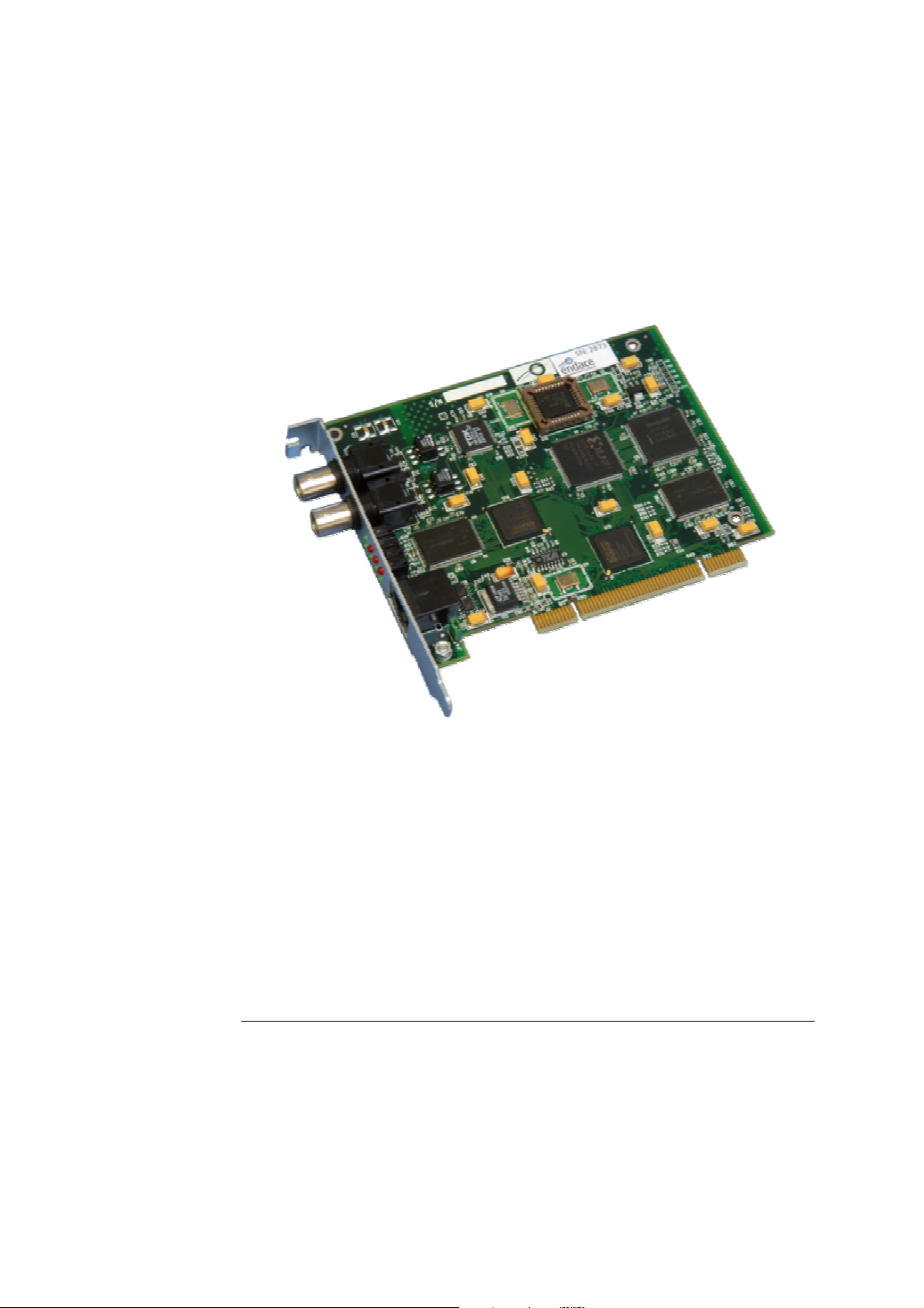
Figure 1-1 shows the DAG 3.6D card.
Figure 1-1. DAG 3.6D Card.
1.3 DAG 3.6D Card Architecture
Description
Because of component close association, packets or cells are time-stamped
accurately.
Time stamped packet records are stored in the lower FPGA, which
interfaces to the PCI bus.
All packet records are written to host PC memory during capture
operations.
Continued on next page
©2005
2 Version 10: May 2006
Page 8
EDM01-14 DAG 3.6D Card User Guide
1.3 DAG 3.6D Card Architecture
, continued
Description
Figure
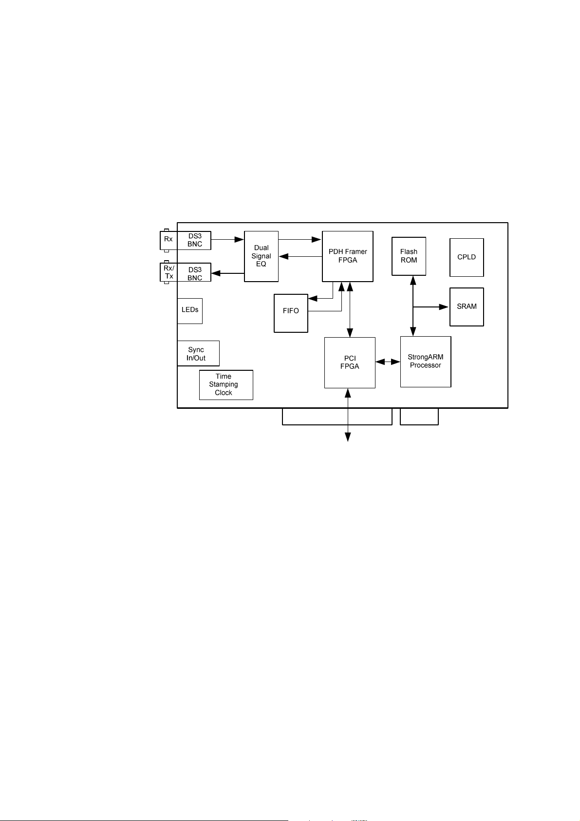
Serial PDH data is received by the DAG 3.6D card co-axial interfaces, and
fed through a Signal Equaliser into the upper of two Xilinx FPGAs.
This FPGA contains a PDH framer and the DUCK timestamp engine. The
close association of these two components means that packets or cells can
be time-stamped very accurately.
Figure 1-2 shows the DAG 3.6D card major components and process
flow.
Figure 1-2. DAG 3.6D Card Major Components and Process Flow.
Time stamped packet or cell records are stored in a FIFO. The DAG 3.6D
can demap either ADM (ATM Direct Mapped) ATM cells, or PLCP
(Payload Layer Convergence Protocol) ATM cells.
Records are then transferred from the FIFO into the lower FPGA, which
has interfaces to the PCI bus and to the bus of the local StrongARM
processor.
The entire record is made available to the StrongARM processor in a
series of memory-mapped registers.
Code running on the StrongARM is then used to decide if the record
should be written to host PC memory over the PCI bus.
©2005
3 Version 10: May 2006
Page 9

EDM01-14 DAG 3.6D Card User Guide
1.4 DAG 3.6D Card Extended Functions
Description
The DAG 3.6D card functionality can be extended in many ways.
The functionality of the 3.6D can be extended in many ways. The user can
develop StrongARM code to filter records, or to collect statistics.
The framer is normally set up to map DS3 payloads, but other mappings
are possible.
For detailed information on device address mapping on the StrongARM
bus, or to discuss the use of other extended features contact the Endace
customer support team at [email protected]
1.5 DAG 3.6D Card System Requirements
Description
Operating
system
Different
system
The DAG 3.6D card and associated data capture system minimum
operating requirements are:
• PC, at least Pentium II 400 MHz, Intel 440BX, GX or newer chip
set
• Minimum of 128 MB RAM
• At least two free PCI free slot with 3.3V and 5V power
• Software distribution free space of 30MB
• Endace Linux Install CD requires 6GB
For convenience, a Debian 3.1 [Sarge] Linux system is included on the
Endace Software Install CD. Endace currently supports Windows XP,
Windows Server 2000, Windows Server 2003, FreeBSD, RHEL 3.0, and
Debian Linux operating systems.
For advice on using a system substantially different from that specified
above, contact Endace support at [email protected]
©2005
4 Version 10: May 2006
Page 10

EDM01-14 DAG 3.6D Card User Guide
2.0 INSTALLING DAG 3.6D CARD
Introduction
A DAG 3.6D card can be installed in any free Bus Mastering PCI slot
The DAG 3.6D card should be the only device on the PCI bus if possible
as the cards make very heavy use of PCI bus data transfer resources.
Although the driver supports up to four DAG cards by default in one
system, due to bandwidth limitations there should not be more than one
card on a single PCI bus. However, this is not usually a limitation as for
most applications a maximum of two cards only can be used with
reasonable application performance.
In this section
This section covers the following topics of information.
• Installation of Operating System and Endace Software
• Insert DAG 3.6D Card into PC
• DAG 3.6D Card Port Connectors
2.1 Installation of Operating System and Endace Software
Description
If the DAG device driver is not installed, before proceeding with the next
chapter, install the software by following the instructions in EDM04-01
Endace Software Installation Manual.
Go to the next chapter of information when the DAG device driver is
installed.
2.2 Insert DAG 3.6D Card into PC
Description
Procedure
Step 1. Access bus Slot
Inserting the DAG 3.6D card into a PC involves accessing the PCI-X bus
slot, fitting the card, and replacing bus slot cover.
Follow these steps to insert the DAG 3.6D card.
Power computer down.
Remove PCI bus slot cover.
Continued on next page
©2005
5 Version 10: May 2006
Page 11

EDM01-14 DAG 3.6D Card User Guide
2.2 Insert DAG 3.6D Card into PC
Procedure (continued)
, continued
Step 2. Fit Card
Insert DAG 3.6D card into PCI bus slot.
Ensure free end fits securely into a card-end bracket that supports the card
weight.
Step 3. Replace bus Slot Screw
Secure card with screw.
Step 4. Power Up Computer
2.3 DAG 3.6D Card Port Connectors
Description
8-pin RJ45
socket
There are two metal co-axial BNC connectors on the DAG 3.6D card.
The top co-axial is Port A, furthest from the PCI slot. The bottom one is
Port B.
Port A is receive only, while port B can be ordered as either a second
receive port or a transmit port. Standard configuration is receive.
The DAG 3.6D has an 8-pin RJ45 socket for the time synchronization
input.
CAUTION: Do not connect the socket to an Ethernet.
©2005
6 Version 10: May 2006
Page 12

EDM01-14 DAG 3.6D Card User Guide
3.0 CONFIDENCE TESTING DAG 3.6D CARD
Introduction
The confidence testing is a process to determine the DAG 3.6D card is
functioning correctly.
The process also involves a card capture session, and demonstrates
configuration in the style of 'What You See You Can Change', WYSYCC.
Interface statistics are also inspected during this process.
In this chapter
This chapter covers the following sections of information.
• DAG 3.6D Card Sensitivity
• Interpreting DAG 3.6D Card LED Status
• DAG 3.6D Card LED Display Functions
• Configuration in WYSYCC style
• DAG 3.6D Card Capture Session
• Reporting Problems
3.1 DAG 3.6D Card Sensitivity
Description
Signal source
specifications
Receiver
capability
Input signal
level
The input signal level to the DAG 3.6D card should be within the dynamic
range of the receiver. If the input signal power is slightly out of range then
an increased bit error rate will be experienced.
If the power is well out of range then the system will be unable to lock to
the PDH frames.
The signal source should meet DS3 template of ANSI-T102.1993 Figure 4
and STS-1 template of ANSIT102.1993 Figure 5, Loss characteristics of
the WE728A or RG 59B cable should be better than Figure C2 of ANSIT102.1993.
The receiver can handle up to 450 feet of cable loss (5.5dB) from the DSX
cross-connect.
The input signal level is measured in mVp, the Peak Differential Input
Amplitude in millivolts.
There is an optional high-gain mode that adds 20dB gain. This is intended
for use with DS3 Monitor signal ports. The DS3 Monitor port is a
resistively attenuated (around -21.5dB) copy of the DSX3 cross connect
signal. The minimum signal level at a DSX3 cross-connect is 360mVp, so
the DSX3 Monitor level at minimum is 30mVp, requiring the high-gain
mode.
Continued on next page
©2005
7 Version 10: May 2006
Page 13
EDM01-14 DAG 3.6D Card User Guide
3.1 DAG 3.6D Card Sensitivity
, continued
Optimum setup
The optimum way to set up a DAG card is to measure the signal level at the
receiver, and to make sure that it is well within the specified range.
Input power can be adjusted, either by changing the splitter ratio if the level
is too high or too low, by inserting an attenuator if the level is too high, or
an amplifier if the level is too low.
Splitters
Passive splitters usually have their insertion losses marked on the package
or in the accompanying documentation.
A 50:50 splitter will have an insertion loss of between 3 dB and 4 dB on
each output. Active splitters may have little or no insertion loss.
3.2 Interpreting DAG 3.6D Card LED Status
Description
Figure
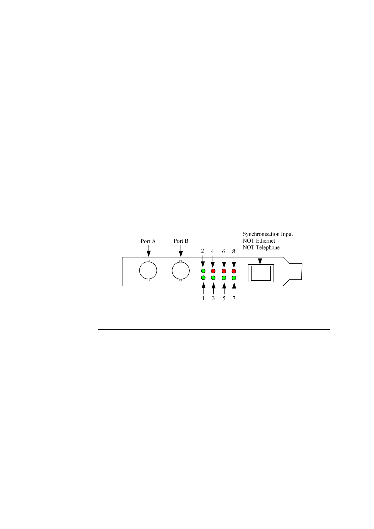
The DAG 3.6D card has status eight LED’s, five coloured green and three
red.
Figure 3-1 shows the DAG 3.6D card status LEDs.
Figure 3-1. DAG 3.6D Card Status LEDs.
Continued on next page
©2005
8 Version 10: May 2006
Page 14
EDM01-14 DAG 3.6D Card User Guide
3.2 Interpreting DAG 3.6D Card LED Status
, continued
LED definitions
The following table describes the LED definitions.
LED Description
LED 1
Upper FPGA successfully programmed.
LED 2 Lower FPGA successfully programmed.
LED 3 Burst Manager Run. Indicates the card is capturing packets
and transferring them to the host.
LED 4 PPS: Pulse Per Second. Indicates card is receiving an
external clock synchronization signal.
LED 5 SDA. Signal Detect Port A.
LED 6
ERRA. Signal error on Port A, equivalent to Loss of Signal
OR Loss of Framing OR Loss of Cell Delineation.
LED 7 SDB. Signal Detect Port B.
LED 8 ERRB: Signal error on Port B, equivalent to Loss of Signal
OR Loss of Framing OR Loss of Cell Delineation.
3.3 DAG 3.6D Card LED Display Functions
Description
Figure
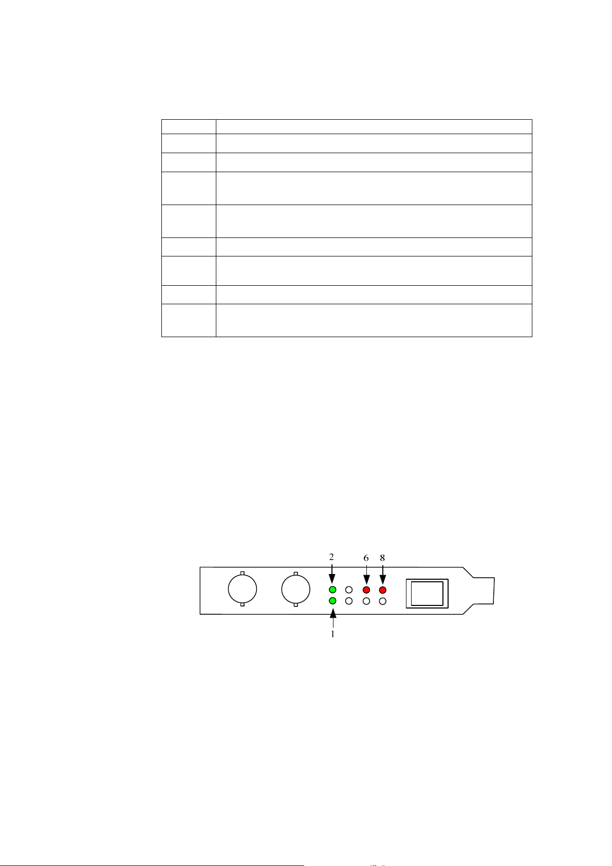
On the DAG 3.6D series of cards LEDs 1 and 2 display when powered up.
When DS3 signals are applied LEDs 6 and 8 should go out, LEDs 5 and 7
should come on. The status of these LEDs should not change during
normal operation of the card.
LED 4 flashes when an external clock synchronization cable is connected
to the RJ45 socket. LED 3 lights when a capture is in progress.
Figure 3-2 shows the correct LED state for the DAG 3.6D card without
input signal.
dagthree
utility
©2005
Figure 3-2. Correct LED State for DAG 3.6D Card Without Input Signal.
The
dagthree
utility supports configuration status and physical layer
interface statistics for the DAG 3.6D card.
When troubleshooting, options
–si
should be passed to the tool to watch
the operational status of the physical, PDH and framing layers. More
details about the meaning of the various bits are supplied through the help
page (
dagthree –h)
as well as via the manual page.
9 Version 10: May 2006
Page 15

EDM01-14 DAG 3.6D Card User Guide
3.4 Configuration in WYSYCC style
Description
Configuration in WYSYCC is the 'What You See You Can Change' style.
Running the command '
dagthree'
Each of the items displayed can be changed as follows:
Configuration
supported
[no]reset
[no]fcl
hold/release framer (in) reset.
(un)set facility loop back. This is useful for card
chaining.
[no]eql
[no]afix
[no]apass
(un)set equipment loop back. Do not touch.
When set correct single bit ATM HEC errors.
(do not)receive cells with HEC errors. Do not
touch.
[no]aidle
[no]ascramble
[no]adm
When set pass through received idle cells. Keep set.
Dis/enable descrambling of ATM cells. Keep set.
(do not)use ATM Cell Direct Mapping, otherwise
PLCP Mapping.
[no]m23
[no]highgain
(do not)use m23 framing, otherwise c-bit framing.
(do not)add 20dB extra gain to Rx.
3.5 DAG 3.6D Card Capture Session
alone shows the current configuration.
Description
Procedure
Step 1. Check Receiver Ports Signal Levels.
Step 2. Understand Link Layer Configuration
The DAG 3.6D card uses the SONET PDH ATM physical layer interface
device to support capturing of ATM. The card supports the DS3 standard.
A successful DAG card capture session is accomplished by checking the
receiver ports optical signal levels and checking the card has correctly
detected the link. This is followed by configuring the DAG card for
normal use.
Follow these steps to troubleshoot DAG card configuration.
Ensure that the signal levels reaching the receiver ports of the card are at the
right levels.
Learn about the link layer configuration in use at the network link being
monitored. Important parameters include m23 Vs. c-bit framing, as well as
the specific scrambling options in use.
If the information cannot be obtained reliably, the card can be made to work
by varying the parameters until data is arriving at the host system.
Continued on next page
©2005
10 Version 10: May 2006
Page 16

EDM01-14 DAG 3.6D Card User Guide
3.5 DAG 3.6D Card Capture Session
, continued
Procedure
Step 3. Check Card is Locked to Data Stream
Step 4. List Current Settings
Step 5. Check FPGA Image Loaded.
, continued
Configure card according to local settings.
Check through the physical layer statistics that the card is locked to the data
stream.
For DAG 3.6D framer configuration and statistics the
supplied.
Calling
The dagthree -h
Before configuring the card, ensure the most recent FPGA image is loaded
on the card.
dag@endace:~$ dagld -d dag0 -x dag/xilinx/dag36pcierf.bit:dag/xilinx/dag36atm-erf.bit
If the FPGA image load fails with the message similar to:
dagld: panic: Cannot replace a d360pci-timed.ncd with a
dag36dpci_atm-erf_pci_v2_2 function image
Add the –f flag to
dagthree
dagthree
without arguments lists current settings.
prints a help listing on tool usage.
dagld
.
Continued on next page
tool is
©2005
11 Version 10: May 2006
Page 17

EDM01-14 DAG 3.6D Card User Guide
3.5 DAG 3.6D Card Capture Session
, continued
Procedure
, continued
Step 6. Configure in WYSYCC Style
dag@endace:~$ dagthree -d dag0
linkA noreset noadm nom23 nohighgain nofcl noeql
atmA noapass ascramble noaidle afix
linkB noreset noadm nom23 nohighgain nofcl noeql
atmB noapass ascramble noaidle afix
packetA drop=0
packetB drop=0
pci 33MHz 32-bit buf=32MB rxstreams=1 txstreams=0 mem=32:0
If the card is configured for c-bit (nom23) framing mode but m23 framing is
required, removing or adding the "no" prefix will change the setting. Type:
dag@endace:~$ dagthree -d dag0 m23
linkA noreset noadm m23 nohighgain nofcl noeql
atmA noapass ascramble noaidle afix
linkB noreset noadm m23 nohighgain nofcl noeql
atmB noapass ascramble noaidle afix
packetA drop=0
packetB drop=0
pci 33MHz 32-bit buf=32MB rxstreams=1 txstreams=0 mem=32:0
3.6 Inspect Interface Statistics
Inspect
interface
statistics
Once the DAG 3.6D card has been configured as expected, the interface
statistics should be inspected to see if the card is locked to the data stream.
dag@endace:~$ dagthree -d dag0 -si
©2005
12 Version 10: May 2006
Page 18

EDM01-14 DAG 3.6D Card User Guide
Status bits
display
The tool will display a number of status bits as they have occurred since
the last time read. In our example, the interval is set to one second via the
-i
option.
LoS
DS3 Loss of Signal.
This indicates that there is no signal at the receiver
LoF
OoF
or signal strength is too low to be recognized.
DS3 Loss of Framing.
DS3 OoF has been asserted for more than 3 ms.
DS3 Out of Framing.
The DS3 Framer is not synchronized.
LoF
PLCP Loss of Frame
PLCP OoF had been asserted for more than 3 ms.
OoE
PLCP Out of Framing
The PLCP Framer is not synchronized
LCD
Loss of cell delineation for 22 or more cells
The ATM state machine has no lock onto the ATM
cell stream.
HEC
Sig
There is an ATM Header Error Code failure.
Line Interface Unit Signal Detect There is a valid
input signal present.
Syn
ATM cell sync.
The ATM cell engine has locked to the ATM cell
stream.
Idle
Cell
An ATM Idle cell is being received.
A non-idle ATM cell is being received.
Continued on next page
©2005
13 Version 10: May 2006
Page 19

EDM01-14 DAG 3.6D Card User Guide
0 0 0 0 0 0 0 1 1 0 0
0 0 0 0 0 0 0 1 1 0 0
0 0 0 0 0 0 0 1 1 0 0
1 1 1 1 1 0 0 0 0 0 0
1 1 1 1 1 0 0 0 0 0 0
1 1 1 1 1 0 0 0 0 0 0
3.6 Inspect Interface Statistics
, continued
Card locked to
An example of a card locked to a DS3 ATM stream is:
DS3 ATM
stream example
A: LoS LoF OoF LoF OoF LCD HEC Fix Sig Syn Idle Cell
0
0
0
No valid signal
example
An example of when there is no valid signal input is:
A: LoS LoF OoF LoF OoF LCD HEC Fix Sig Syn Idle Cell
1
1
1
Status bits
The PLCP LoF and OoF status bits are not valid during ADM operation,
and will read as 0.
General
purpose
counters
Programmable counters are not available on the DAG 3.6D with this
release.
Test trace
If those tests provide a satisfactory status, a test trace should be taken. We
suggest a 10 seconds trace file by passing the option
-s 10
to
dagsnap
along with option -v for more user information.
,
©2005
14 Version 10: May 2006
Page 20
EDM01-14 DAG 3.6D Card User Guide
3.7 Reporting Problems
Description
Problem
checklist
If there are unresolved problems with a DAG card or supplied software,
contact Endace Technical Support via the email address
Supplying sufficient information in an email enables effective response.
The exact information available to users for trouble, cause and correction
analysis may be limited by nature of the problem. The following items
assist a quick problem resolution:
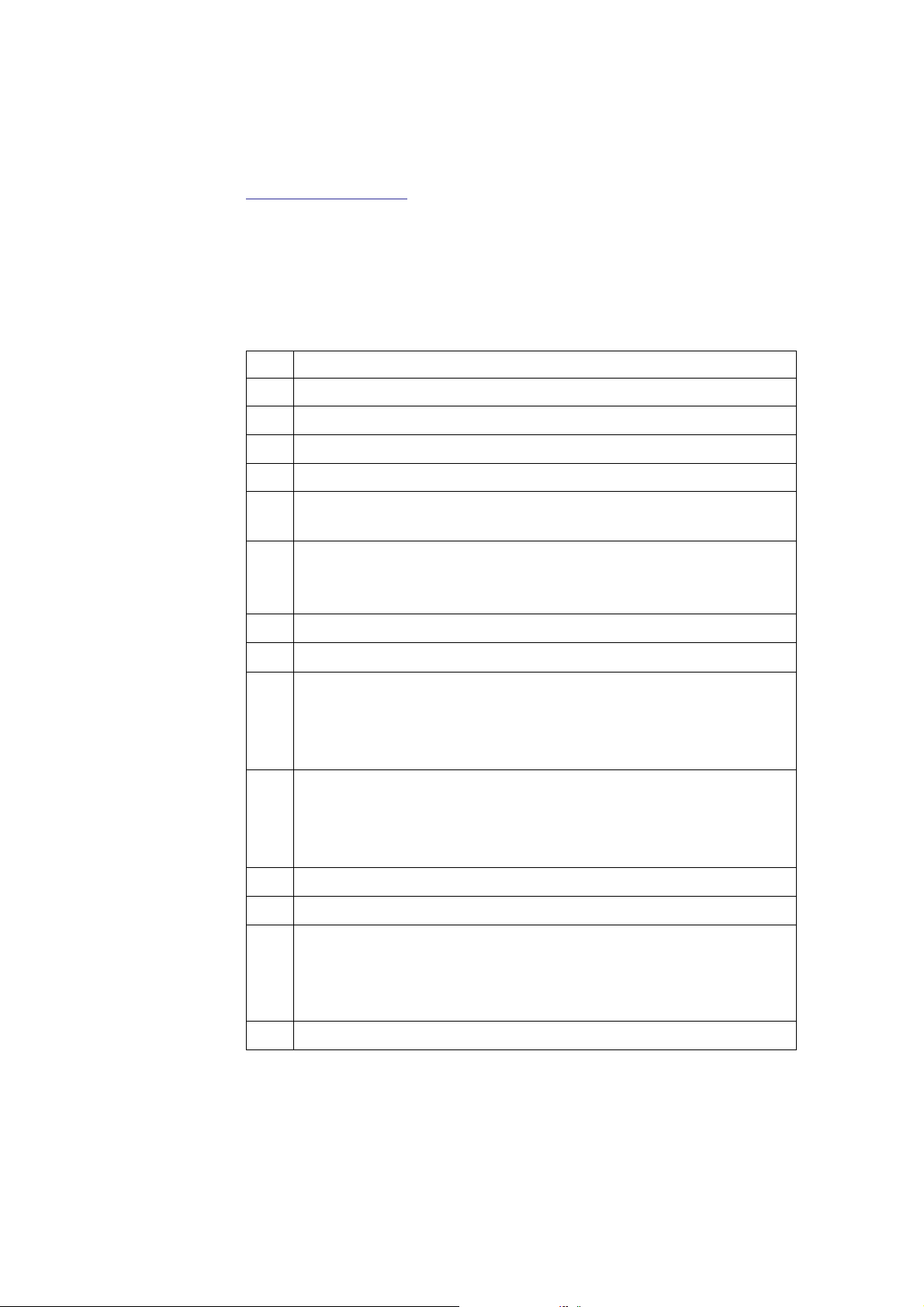
Ref Item
1. DAG card[s] model and serial number.
2. Host PC type and configuration.
3. Host PC operating system version.
4. DAG software version package in use.
5. Any compiler errors or warnings when building DAG driver or
tools.
6. For Linux and FreeBSD, messages generated when DAG device
driver is loaded. These can be collected from command
or from log file
/var/log/syslog.
dmesg
,
7.
Output of
8.
Firmware versions from
daginf
.
dagbug –cx
.
9. Physical layer status reported by:
dagthree
10. Network link statistics reported by:
dagthree –si
11. Network link configuration from the router where available.
12. Contents of any scripts in use.
13. Complete output of session where error occurred including any
error messages from DAG tools. The
typescript
Unix utility
may be useful for recording this information.
14,. A small section of captured packet trace illustrating the problem.
©2005
15 Version 10: May 2006
Page 21

EDM01-14 DAG 3.6D Card User Guide
©2005
16 Version 10: May 2006
Page 22

EDM01-14 DAG 3.6D Card User Guide
©2005
17 Version 10: May 2006
Page 23

EDM01-14 DAG 3.6D Card User Guide
4.0 RUNNING DATA CAPTURE SOFTWARE
Introduction
Running the data capture software involves starting the capture session
followed by checking the high load performance.
In this chapter
This chapter covers the following sections of information.
• Starting Capture Session
• High Load Performance
4.1 Starting Capture Session
Description
drv/dagload
tools/dagld -d dag0 -x xilinx/dag36pci-erf.bit:xilinx/dag36atm-erf.bit
Process
The various tools used for data capture are in the
tools
sub-directory.
For a typical measurement session, first move to the
dag
directory, load the
driver, then load the appropriate Xilink receive image to each DAG card.
For example, with two DAG 3.6D cards installed:
The integrity of the card’s physical layer is then set and the integrity of the
physical layer to both DAG cards checked.
For ATM Direct Mapping the ‘
while for PLCP ATM Mapping the ‘
dagthree adm
dagthree noadm
’ option should be used,
’ should be used.
Follow this process to set a data capture session.
Process Description
Set and check integrity
of card physical layer.
Starting capture
session.
For example:
dagthree –d dag0 default
Use:
tools/dagsnap v –o tracefile
The option -v is used to provide user
information during capture; it may be wanted to
omit it for automated trace runs.
If the –o
the tool will write to
to pipeline
dagtools
tracefile
dagsnap
package.
parameter is not specified
stdout
, which can be used
with other tools from the
Continued on next page
©2005
18 Version 10: May 2006
Page 24

EDM01-14 DAG 3.6D Card User Guide
4.1 Starting Capture Session
, continued
Process
, continued
Process Description
Stopping
dagsnap
4.2 High Load Performance
Description
Avoiding
packet loss
Reading records
Detecting
packet losses
As the DAG 3.6D card captures packets from the network link, it writes a
record for each packet into a large buffer in the host PC’s main memory.
In order to avoid packet loss, the user application reading the record, such
as
dagsnap
, must be able to read records out of the buffer faster than they
arrive, otherwise the buffer eventually fills, and packet records are lost.
When the PC buffer fills, the message:
kernel: dagN: pbm safety net reached 0xNNNNNNNN
is displayed on the PC screen, and printed to log
The “Data capture” LED also goes out. This may be visibly indicated as
flashing or flickering.
In order to avoid any potential packet loss, the user process must read
records faster than they arrive from the network.
If the user process is writing records to hard disk, it may be necessary to
use a faster disk or disk array. If records are being processed in real-time, a
faster host CPU may be required.
Until some data is read out of the buffer to free some space, any arriving
packets subsequently are discarded by the DAG card. Any loss is detected
in-band by observing the Loss Counter
Record Format [ERF]. The Endace ERF is detailed in Chapter 7 of this
document.
By default
can be stopped with a signal:
killall dagsnap
dagsnap
fixed number of seconds and then exit.
dagsnap
will run forever.
dagsnap
can also be configured to run for a
/var/log/messages
lctr
field of the Extensible
Continued on next page
.
©2005
19 Version 10: May 2006
Page 25

EDM01-14 DAG 3.6D Card User Guide
4.2 High Load Performance
, continued
Increasing
buffer size
The host PC buffer can be increased to deal with bursts of high traffic load
on the network link. By default the
dagmem
driver reserves 32MB of
memory per DAG card in the system.
For OC-12/STM-4 (622Mbps) rates and above, 128MB or more may be
required per card. To change the amount of memory reserved, edit the file
/etc/modules
. If the Endace Install CD has been used it will include this
section:
# For DAG 3.x, default 32MB/card
dagmem
#
# For DAG 4.x or 6.x, use more memory per card, E.G.
# dagmem dsize=128m
The option
system. The value of
dsize
sets the amount of memory used per DAG card in the
dsize
multiplied by the number of DAG cards must
be less than the amount of physical memory installed, and must be less
than 890MB.
©2005
20 Version 10: May 2006
Page 26

EDM01-14 DAG 3.6D Card User Guide
©2005
21 Version 10: May 2006
Page 27

EDM01-14 DAG 3.6D Card User Guide
5.0 SYNCHRONIZING CLOCK TIME
Description
DUCK
configuration
Common
synchronization
In this chapter
The Endace DAG range of products come with sophisticated time
synchronization capabilities, in order to provide high quality timestamps,
optionally synchronized to an external time standard.
The system that provides the DAG synchronization capability is known as
the DAG Universal Clock Kit (DUCK).
An independent clock in each DAG card runs from the PC clock. A
card’s clock is initialised using the PC clock, and then free-runs using a
crystal oscillator.
Each card's clock can vary relative to a PC clock, or other DAG cards.
The DUCK is configured to avoid time variance between sets of DAG
cards or between DAG cards and coordinated universal time [UTC].
Accurate time reference can be obtained from an external clock by
connecting to the DAG card using the synchronization connector, or the
host PCs clock can be used in software as a reference source without
additional hardware.
Each DAG card can also output a clock signal for use by other cards.
The DAG card synchronization connector supports a Pulse-Per-Second
(PPS) input signal, using RS-422 signalling levels.
Common synchronization sources include GPS or CDMA (Cellular
telephone) time receivers.
Endace produces the TDS 2 Time Distribution Server modules and the
TDS 6 units that enable multiple DAG cards to be connected to a single
GPS or CDMA unit.
More information is on the Endace website,
http://www.endace.com/accessories.htm, or the TDS 2/TDS 6 Units
Installation Manual.
This chapter covers the following sections of information.
©2005
• Configuration Tool Usage
• Time Synchronization Configurations
• Synchronization Connector Pin-outs
22 Version 10: May 2006
Page 28

EDM01-14 DAG 3.6D Card User Guide
5.1 Configuration Tool Usage
Description
Example
dag@endace:~$ dagclock –d dag0
muxin rs422
muxout none
status Synchronized Threshold 596ns Failures 0 Resyncs 0
error Freq -30ppb Phase -60ns Worst Freq 75ppb Worst Phase 104ns
crystal Actual 100000028Hz Synthesized 67108864Hz
input Total 3765 Bad 0 Singles Missed 5 Longest Sequence Missed 1
start Thu Apr 28 13:32:45 2005
host Thu Apr 28 14:35:35 2005
dag Thu Apr 28 14:35:35 2005
The DUCK is very flexible, and can be used in several ways, with or
without an external time reference source. It can accept synchronization
from several input sources, and can also be made to drive its
synchronization output from one of several sources.
Synchronization settings are controlled by the
dag@endace:~$ dagclock -h
Usage: dagclock [-hvVxk] [-d dag] [-K <timeout>] [-l
<threshold>] [option]
dagclock
utility.
-h --help,--usage this page
-v --verbose increase verbosity
-V --version display version information
-x --clearstats clear clock statistics
-k --sync wait for duck to sync before
exiting
-d dag DAG device to use
-K timeout sync timeout in seconds, default
60
-l threshold health threshold in ns, default
596
Option:
default RS422 in, none out
none None in, none out
rs422in RS422 input
hostin Host input (unused)
overin Internal input (synchronize to
host clock)
auxin Aux input (unused)
rs422out Output the rs422 input signal
loop Output the selected input
hostout Output from host (unused)
overout Internal output (master card)
set Set DAG clock to PC clock
reset Full clock reset. Load time
from PC, set rs422in, none out
By default, all DAG cards listen for synchronization signals on their RS422 port, and do not output any signal to their RS-422 port.
©2005
23 Version 10: May 2006
Page 29

EDM01-14 DAG 3.6D Card User Guide
5.2 Time Synchronization Configurations
Description
The DUCK is very flexible, and can be used in several ways, with or
without an external time reference source.
The use includes a single card with no reference, two cards with no
reference, and a card with reference.
In this section
This section covers the following topics of information.
• Single Card no Reference Time Synchronization
• Two Cards no Reference Time Synchronization
• Card with Reference Time Synchronization
5.2.1 Single Card no Reference Time Synchronization
Description
dag@endace:~$ dagclock –d dag0 none overin
muxin overin
muxout none
status Synchronized Threshold 11921ns Failures 0 Resyncs 0
error Freq 1836ppb Phase 605ns Worst Freq 143377ppb Worst Phase
88424ns
crystal Actual 49999347Hz Synthesized 16777216Hz
input Total 87039 Bad 0 Singles Missed 0 Longest Sequence Missed 0
start Wed Apr 27 14:27:41 2005
host Thu Apr 28 14:38:20 2005
dag Thu Apr 28 14:38:20 2005
When a single card is used with no external reference, the card can be
synchronized to the host PC’s clock.
The clock in most PC’s is not very accurate by itself, but the DUCK drifts
smoothly at the same rate as the PC clock.
If a PC is running NTP to synchronize its own clock, then the DUCK
clock is less smooth because the PC clock is adjusted in small jumps.
However, overall the DUCK clock does not drift away from UTC.
The synchronization achieved in this case is not as accurate as when using
an external reference source such as GPS.
The DUCK clock is synchronized to a PC clock by setting input
synchronization selector to overflow:
NOTE:
dagclock
should be run only after appropriate Xilinx images have
been loaded. If the Xilinx images must be reloaded, the
command must be rerun afterwards to restore the configuration.
dagclock
©2005
24 Version 10: May 2006
Page 30

EDM01-14 DAG 3.6D Card User Guide
5.2.2 Two Cards no Reference Time Synchronization
Description
Synchronizing
cards
Locking cards
together
dag@endace:~$ dagclock –d dag0 none overout
muxin none
muxout over
status Not Synchronized Threshold 596ns Failures 0 Resyncs 0
error Freq 0ppb Phase 0ns Worst Freq 0ppb Worst Phase 0ns
crystal Actual 100000000Hz Synthesized 67108864Hz
input Total 0 Bad 0 Singles Missed 0 Longest Sequence Missed 0
start Thu Apr 28 14:48:34 2005
host Thu Apr 28 14:48:34 2005
dag No active input - Free running
When two DAG cards are used in a single host PC with no reference
clock, the cards are to be synchronized in some way if timestamps
between the two cards are to be compared. For example, if two cards
monitor different directions of a single full-duplex link.
Synchronization between two DAG cards is achieved in two ways. One
card can be a clock master for the second, or one can synchronize to the
host and also act as a master for the second.
If both cards are to be accurately synchronized, but not so for absolute
time of packet time-stamps being correct, then one card is configured as
the clock master for the other.
Although the master card’s clock will drift against UTC, the cards are
locked together.
The cards are locked together by connecting the synchronization
connector ports of both cards with a standard RJ-45 Ethernet cross-over
cable.
Configure one of the cards as the master, the other defaults to being a
slave.
The slave card configuration is not shown, the default configuration is
sufficient.
Continued on next page
©2005
25 Version 10: May 2006
Page 31

EDM01-14 DAG 3.6D Card User Guide
5.2.2 Two Cards no Reference Time Synchronization
, continued
Preventing
time-stamps
drift
To prevent the DAG card clocks time-stamps drifting against UTC, the
master can be synchronized to the host PC’s clock which in turn utilises
NTP. This then provides a master signal to the slave card.
The cards are locked together by connecting the synchronization
connector ports of both cards with a standard RJ-45 Ethernet cross-over
cable.
Configure one card to synchronize to the PC clock and output a RS-422
synchronization signal to the second card.
dag@endace:~$ dagclock –d dag0 none overin overout
muxin over
muxout over
status Synchronized Threshold 11921ns Failures 0 Resyncs 0
error Freq -691ppb Phase -394ns Worst Freq 143377ppb Worst Phase
88424ns
crystal Actual 49999354Hz Synthesized 16777216Hz
input Total 87464 Bad 0 Singles Missed 0 Longest Sequence Missed 0
start Wed Apr 27 14:27:41 2005
host Thu Apr 28 14:59:14 2005
dag Thu Apr 28 14:59:14 2005
The slave card configuration is not shown, the default configuration is
sufficient.
5.2.3 Card with Reference Time Synchronization
Description
Pulse signal
from external
sources
The best timestamp accuracy occurs when a DAG card is connected to an
external clock reference, such as a GPS or CDMA time receiver.
The DAG synchronization connector accepts a RS-422 Pulse Per Second
[PPS] signal from external sources.
This is derived directly from a reference source, or distributed through the
Endace TDS 2 [Time Distribution Server] module which allows two DAG
cards to use a single receiver.
More cards can be accommodated by daisy-chaining TDS-6 expansion
units to the TDS-2 unit, each providing outputs for an additional 6 DAG
cards.
Continued on next page
©2005
26 Version 10: May 2006
Page 32

EDM01-14 DAG 3.6D Card User Guide
5.2.3 Card with Reference Time Synchronization
, continued
Using external
reference
source
To use an external clock reference source, the host PC’s clock must be
accurate to UTC to within one second. This is used to initialise the
DUCK.
The external time reference allows high accuracy time synchronization.
When the time reference source is connected to the DAG card
synchronization connector, the card automatically synchronizes to a valid
signal.
dag@endace:~$ dagclock –d dag0
muxin rs422
muxout none
status Synchronized Threshold 596ns Failures 0 Resyncs 0
error Freq 30ppb Phase -15ns Worst Freq 2092838ppb Worst Phase 33473626ns
crystal Actual 100000023Hz Synthesized 67108864Hz
input Total 225 Bad 0 Singles Missed 1 Longest Sequence Missed 1
start Thu Apr 28 14:55:20 2005
host Thu Apr 28 14:59:06 2005
dag Thu Apr 28 14:59:06 2005
Connecting
time
distribution
server
The TDS 2 module connects to any DAG card with a standard RJ-45
Ethernet cable and can be placed some distance from a DAG card.
Existing RJ-45 building cabling infrastructure can be used to cable
synchronization ports.
CAUTION: Never connect a DAG card and/or the TDS 2 module to
active Ethernet or telephone equipment.
Testing signal
For Linux and FreeBSD, when a synchronization source is connected the
driver outputs some messages to the console log file
/var/log/messages
The
dagpps
tool is used to test a signal is being received correctly and is
of correct polarity. To perform the test, run:
dagpps –d dag0.
The tool measures input state many times over several seconds, displaying
polarity and length of input pulse.
Some DAG cards have LED indicators for synchronization (PPS) signals.
.
©2005
27 Version 10: May 2006
Page 33
EDM01-14 DAG 3.6D Card User Guide
5.3 Synchronization Connector Pin-outs
Description
Pin assignments
Figure
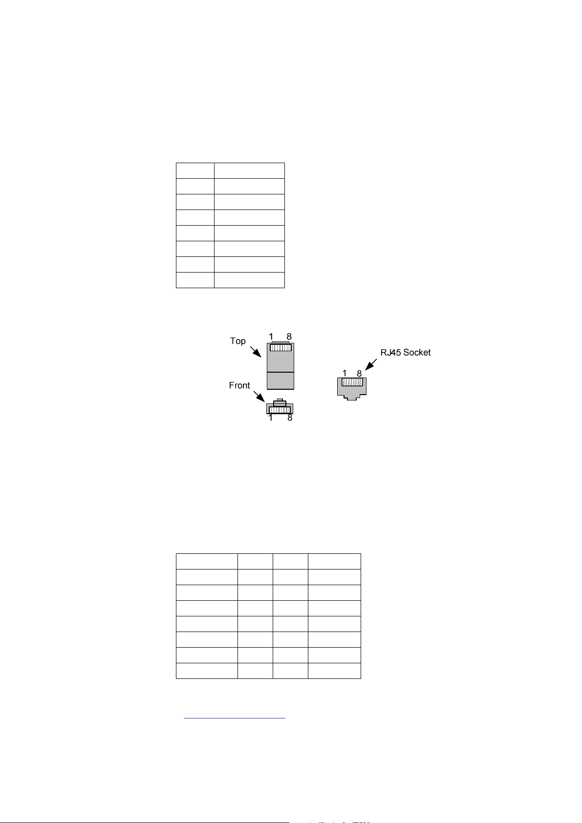
DAG cards have an 8-pin RJ45 connector with two bi-directional RS422
differential circuits, A and B. The PPS signal is carried on circuit A, and
the serial packet is connected to the B circuit.
The 8-pin RJ45 connector pin assignments are:
1. Out A+
2. Out A-
3. In A+
4. In B+
5. In B-
6. In A-
7. Out B+
8. Out B-
Figure 6-1 shows the RJ45 plug and socket connector pin-outs.
Out-pin
connections
Ethernet
crossover cable
Support
Figure 6-1. RJ45 Plug and Socket Connector Pin-outs.
Normally the GPS input should be connected to the A channel input, pins
3 and 6. The DAG card can also output a synchronization pulse; used
when synchronizing two DAG cards without a GPS input.
Synchronization output is generated on the Out A channel, pins 1 and 2.
A standard Ethernet crossover cable can be used to connect the two cards.
TX_A+ 1 3 RX_A+
TX_A- 2 6 RX-ARX_A+ 3 1 TX_A+
RX_B+ 4 7 TX_B+
RX_B- 5 8 TX_BRX_A- 6 2 TX_ATX_B+ 7 4 RX_B+
TX_B- 8 5 RX_B-
For cables and further advice on using GPS and CDMA time receivers
email [email protected].
©2005
28 Version 10: May 2006
Page 34

EDM01-14 DAG 3.6D Card User Guide
©2005
29 Version 10: May 2006
Page 35
EDM01-14 DAG 3.6D Card User Guide
6.0 DATA FORMATS OVERVIEW
In this chapter
This chapter covers the following sections of information.
• Data Formats
• Timestamps
6.1 Data Formats
Description
Table
Data format
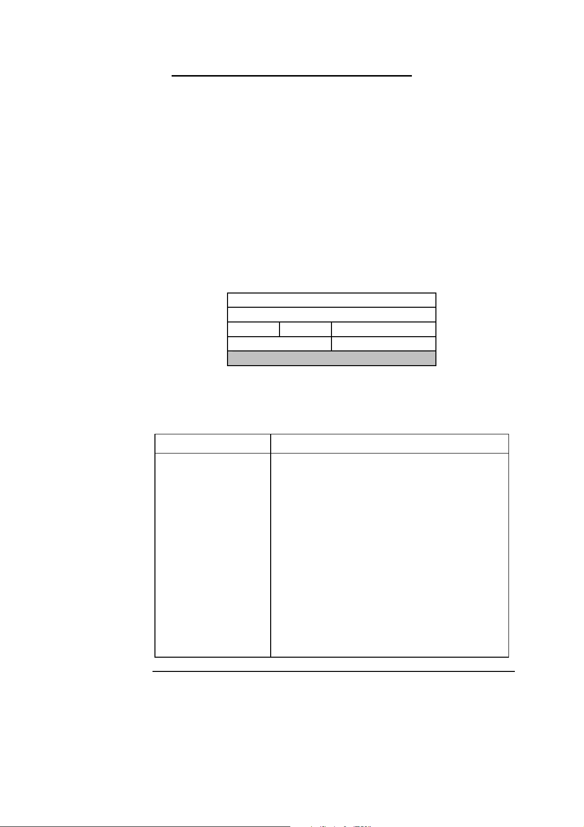
The DAG card uses the ERF Type 3 ATM Cell. Timestamps are in littleendian [Pentium native] byte order. All other fields are in big-endian
[network] byte order. All payload data is captured as a byte stream, no
byte re-ordering is applied.
Table 7-1 shows the generic variable length record. The diagram is not to
scale.
The following is an overview of the data format used.
timestamp
timestamp
type flags rlen
lctr wlen
(rlen - 16) bytes of record
Table 7-1. Generic Variable Length Record.
Data Format Description
type: This field contains an enumeration of the frame
subtype. If the type is zero, then this is a legacy
format.
0: TYPE_LEGACY
1: TYPE_HDLC_POS: PoS w/HDLC framing
2: TYPE_ETH: Ethernet
3: TYPE_ATM: ATM Cell
4: TYPE_AAL5: reassembled AAL5 frame
5: TYPE_MC_HDLC: Multi-channel HDLC
frame
6: TYPE_MC_RAW: Multi-channel Raw link
data
7: TYPE_MC_ATM: Multi-channel ATM Cell
Continued on next page
©2005
30 Version 10: May 2006
Page 36
EDM01-14 DAG 3.6D Card User Guide
Packet length including some protocol overhead.
6.1 Data Formats
, continued
Data Format Description
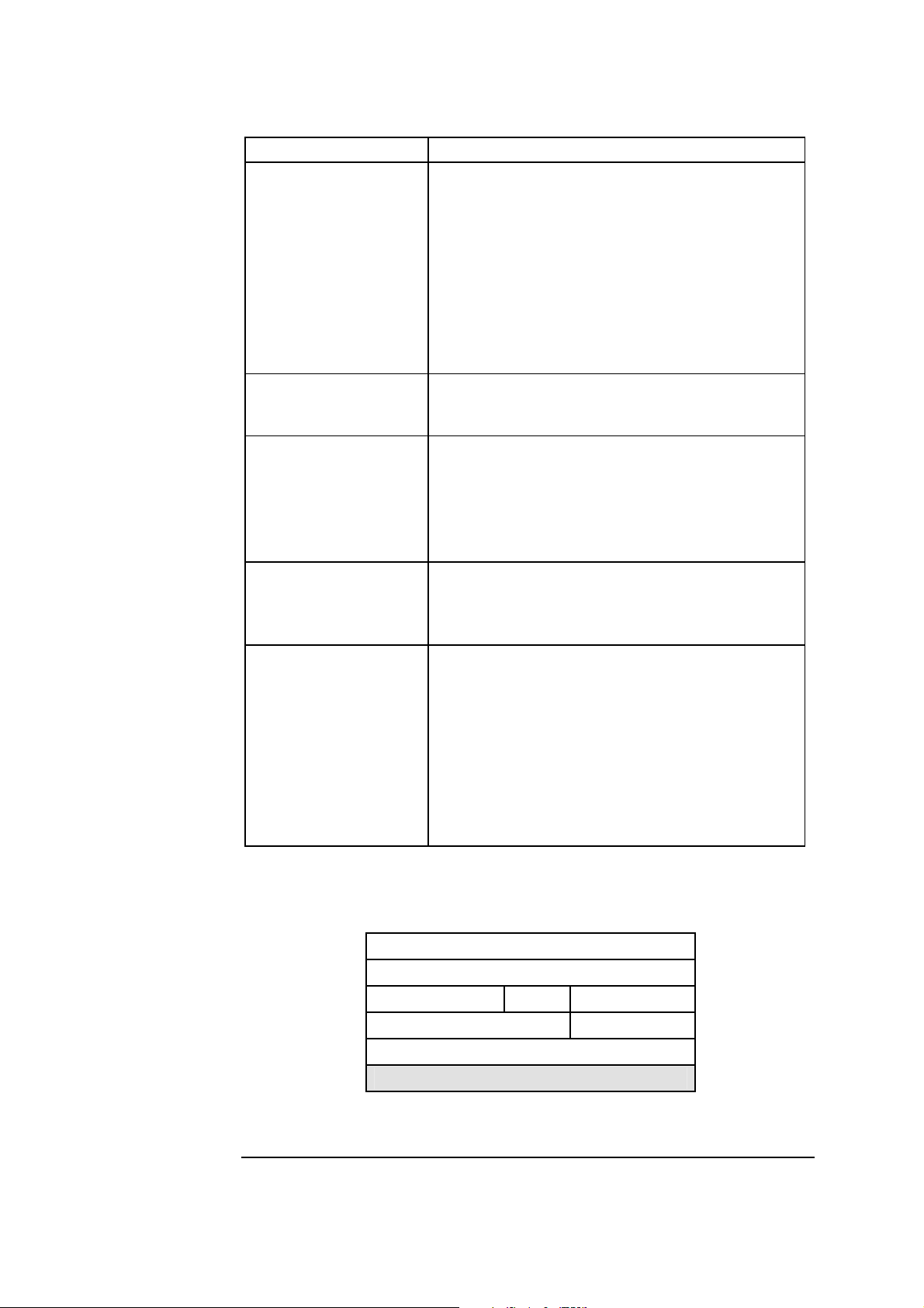
flags: This byte is divided into 2 parts, the interface
identifier, and the capture offset.
1-0: capture interface 0-3
2: varying record lengths present
3: truncated record [insufficient buffer space]
4: rx error [link error]
5: 5: ds error [internal error]
7-6: reserved
Rlen: record length Total length of the record transferred over PCI
bus to storage.
Lctr: loss counter A 16 bit counter, recording the number of
packets lost since the previous record. Records
can be lost between the DAG card and memory
hole due to overloading on PCI bus. The
counter starts at zero, and sticks at 0xffff.
Wlen: wire length
The exact interpretation of this quantity depends
on physical medium.
offset: Number of bytes *not* captured from start of
frame.
Typically used to skip link layer headers when
not required in order to save bandwidth and
space.
This field is currently not implemented, contents
can be disregarded.
Figure
Figure 6-2 shows the Type 1 PoS HDLC Variable Length Record. The
diagram is not to scale.
timestamp
©2005
timestamp
type:1 flags rlen
lctr wlen
HDLC Header
(rlen - 20) bytes of packet
Type 1 PoS HDLC Variable Length Record.
Continued on next page
31 Version 10: May 2006
Page 37
EDM01-14 DAG 3.6D Card User Guide
6.1 Data Formats
, continued
Table
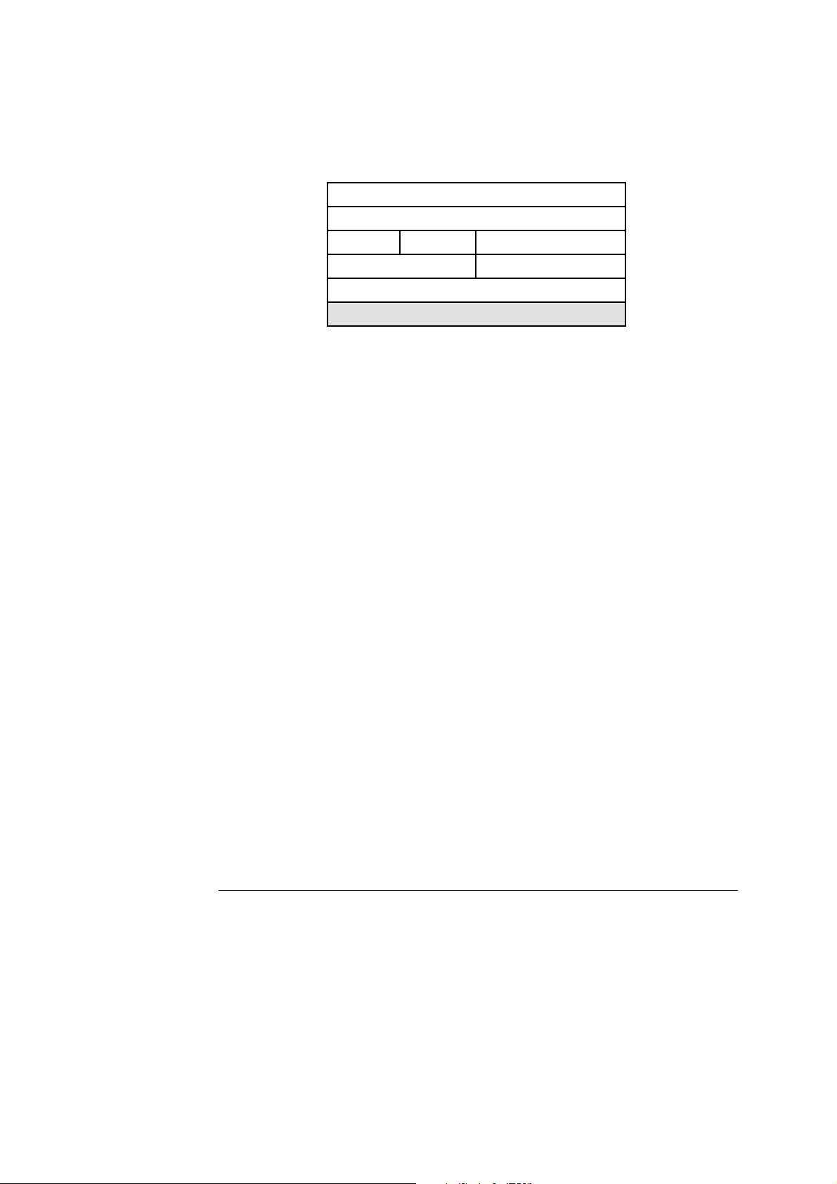
Table 6- 3 shows the Type 3 ATM Cell Record. The diagram is not to
scale.
The ethernet frame begins immediately after the pad byte so that the layer
3 (IP) header is 32Bit-aligned.
6.2 Timestamps
Description
The ERF format incorporates a hardware generated timestamp of the
packet’s arrival.
The format of this timestamp is a single little-endian 64-bit fixed point
number, representing seconds since midnight on the first of January 1970.
The high 32-bits contain the integer number of seconds, while the lower
32-bits contain the binary fraction of the second. This allows an ultimate
resolution of 2
Another advantage of the ERF timestamp format is that a difference
between two timestamps can be found with a single 64-bit subtraction. It
is not necessary to check for overflows between the two halves of the
structure as is needed when comparing Unix time structures, which are
also available to Windows user in the Winsock library.
Different DAG cards have different actual resolutions. This is
accommodated by the lowermost bits that are not active being set to zero.
In this way the interpretation of the timestamp does not need to change
when higher resolution clock hardware is available.
timestamp
timestamp
type:3 flags rlen
lctr wlen
ATM Header
48 bytes of cell
Table 6-3. Generic Variable Length Record.
-32
seconds, or approximately 233 picoseconds.
Continued on next page
©2005
32 Version 10: May 2006
Page 38

EDM01-14 DAG 3.6D Card User Guide
6.2 Timestamps
, continued
Example codes
Here is some example code showing how a 64-bit ERF timestamp (erfts)
can be converted into a struct timeval representation (tv).
unsigned long long lts;
struct timeval tv;
lts = erfts;
tv.tv_sec = lts >> 32;
lts = ((lts & 0xffffffffULL) * 1000 * 1000);
lts += (lts & 0x80000000ULL) << 1; /* rounding */
tv.tv_usec = lts >> 32;
if(tv.tv_usec >= 1000000) {
tv.tv_usec -= 1000000;
tv.tv_sec += 1;
}
©2005
33 Version 10: May 2006
 Loading...