

EM Microelectronic V6309LSP3B, V6309MSP3B, V6309RSP3B, V6309SSP3B, V6309TSP3B Schematic [ru]
...
V
V
R
EM MICROELECTRONIC -
3-Pin Microprocessor Reset Circuit
Description
The V6309 and V6319 are microprocessor supervisory
circuits used to monitor the power supplies in µP and digital
systems. They provide excellent circuit reliability and low
cost by eliminating external components and adjustments
when used with 5V powered or 3V powered circuits.
These circuits perform a single function: they assert a reset
signal whenever the V
preset threshold, keeping it asserted for at least 140ms after
VDD has risen above the reset threshold. The only difference
between the two devices is that the V6309 has an active-low
RESET output (which is guaranteed to be in the correct
state for V
down to 1V), while the V6319 has an active-
DD
high RESET output. The reset comparator is designed to
ignore fast transients on V
operation with a variety of supply voltages are available.
Low supply current makes the V6309/V6319 ideal for use in
portable equipment. The V6309/V6319 come in a 3-pin
SOT23 package.
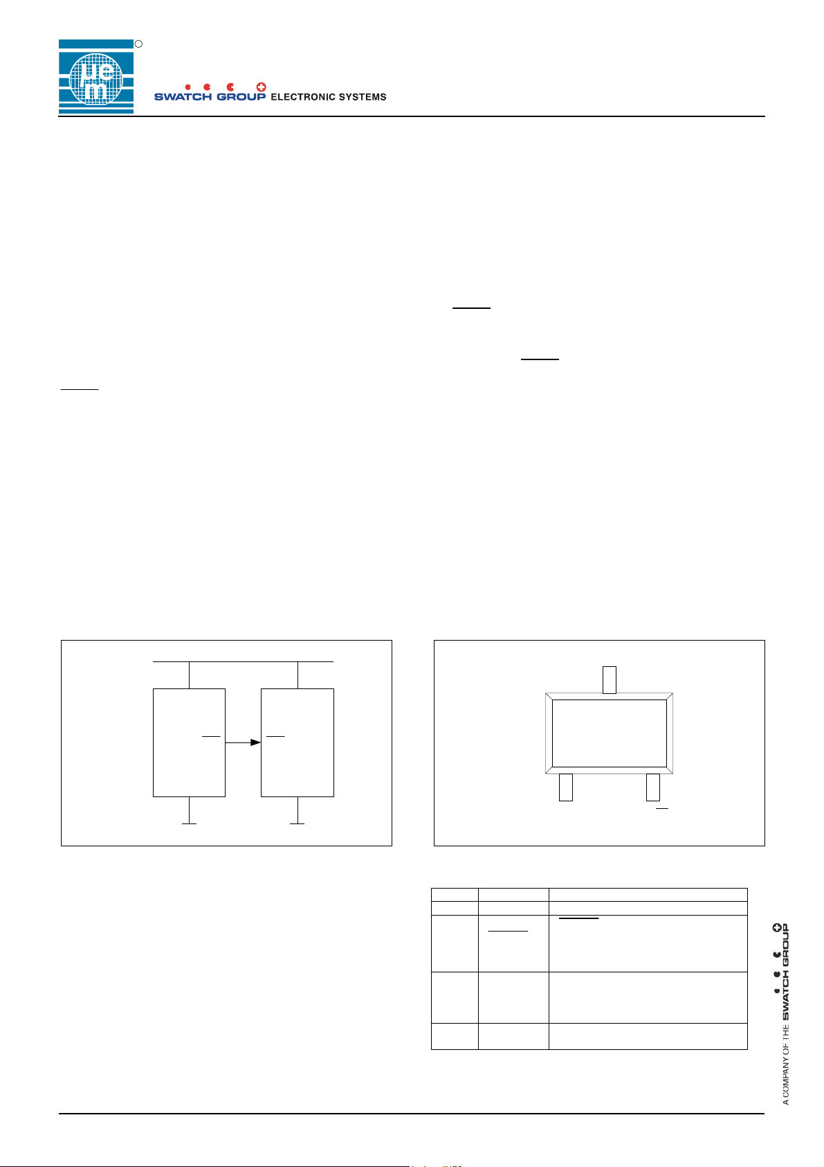
Typical Operating Configuration
V
DD
supply voltage declines below a
DD
. Reset thresholds suitable for
DD
MARIN SA
6309
6319
Features
Precision monitoring of 3V, 3.3V and 5V power supply
voltages
Fully specified over the temperature range of
-40 to +125°C
140ms minimum power-on reset pulse width:
RESET output for V6309
RESET output for V6319
16 µA supply current
Guaranteed RESET/RESET valid to V
Power supply transient immunity
No external components needed
3-pin SOT23 package
Fully compatible with MAX809/MAX810
Applications
Computer
Controllers
Intelligent instruments
Critical µP and µC power monitoring
Portable/battery-powered equipment
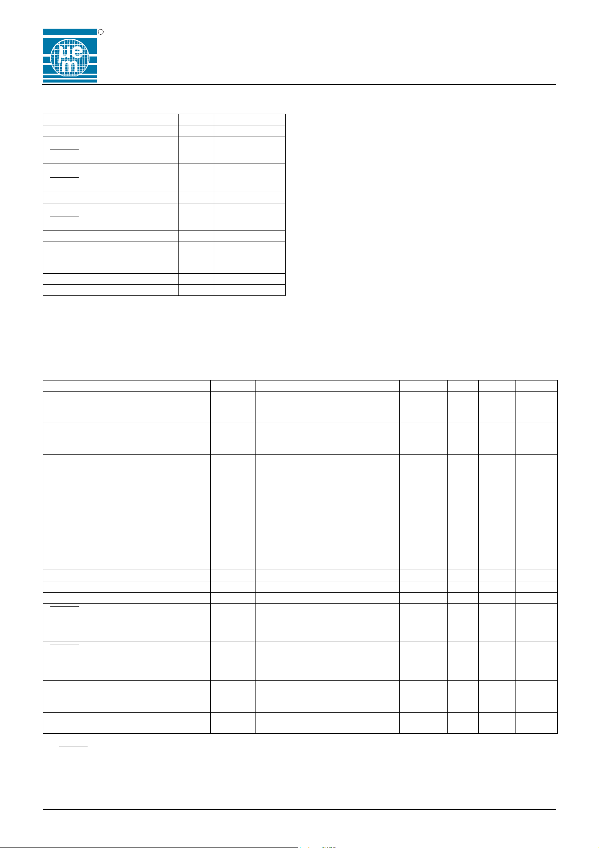
Pin Assignment
SOT23-3L
V
DD
DD
= 1V
V
DD
V6309
V
SS
RES
V
DD
Micro-
processor
RES
V
SS
V
Fig. 1
Pin Description
Pin Name Function
1 VSS Ground
2 for V6309
RESET
2 for V6319
RESET
3 VDD Supply voltage (+5V, +3.3V or
SS
RESET
V
DD
rises for 240ms after V
reset threshold
RESET Output remains high while
V
DD
rises for 240ms after V
reset threshold
+3.0V)
3
V6309/19
21
RES / RES
Output remains low while
is below the reset threshold and
is below the reset threshold and
above the
DD
above the
DD
Table 1
Fig. 2
Copyright © 2005, EM Microelectronic-Marin SA
1
www.emmicroelectronic.com
V
V
R
6309
Absolute Maximum Ratings
Parameter Symbol Conditions
Terminal voltage to VSS V
Min. voltage at RESET or
RESET
Maximum voltage at RESET or
RESET
Input current at VDD I
Output current at RESET or
RESET
Rate of rise at VDD t
Stresses above these listed maximum ratings may cause
-0.3V to + 6.0V
DD
permanent damages to the device. Exposure beyond
specified operating conditions may affect device reliability or
V
-0.3V
min
cause malfunction.
V
VCC + 0.3V
max
20 mA
min
I
20 mA
max
100Vµs
R
Handling Procedures
This device has built-in protection against high static
voltages or electric fields; however, it is advised that normal
precautions be taken as for any other CMOS component.
Unless otherwise specified, proper operation can only occur
when all terminal voltages are kept within the voltage range.
6319
Continuous power dissipation at
T
= +70°C for SOT-23
A
320 mW
P
max
(>70°C derate by 4 mW/°C)
Operating temperature range TA -40 to +125°C
Storage temperature range TST -65°C to +150°C
Table 2
Electrical Characteristics
VDD = full range, TA = -40 to +125°C, unless otherwise specified, typical values at TA = +25°C, VDD = 5V for versions L and M,
V
= 3.3V for versions T and S, VDD = 3 V for R. (Production testing done at TA = +25°C and 85°C, over temperature limits
DD
guaranteed by design only)
Parameter Symbol Test Conditions Min. Typ. Max. Unit
VDD range VDD TA = 0 to +70°C 1.0 5.5 V
T
T
Supply current
versions L, M ICC VDD < 5.5V 26 60 µA
versions R, S, T VDD < 3.6V 16 50 µA
RESET threshold 1)
version L VTH TA = +25°C 4.56 4.63 4.70 V
T
version M TA = +25°C 4.31 4.38 4.45 V
T
version T TA = +25°C 3.04 3.08 3.11 V
T
version S TA = +25°C 2.89 2.93 2.96 V
T
version R TA = +25°C 2.59 2.63 2.66 V
T
Reset threshold temp. coefficient -200 ppm/°C
VDD to reset delay 1) V
Reset active timeout period TA = -40 to °125°C 140 330 590 ms
RESET output voltage low for V6309
V
OL
versions R, S, T VDD = VTH min., I
versions L, M VDD = VTH min., I
RESET output voltage high for V6309
versions R, S, T VOH VDD = VTH max., I
versions L, M VDD = VTH max., I
RESET output voltage low for V6319
versions R, S, T VOL VDD = VTH max., I
versions L, M VDD = VTH max., I
RESET output voltage high for V6319 VOH 1.8V < VDD < VTH min.,
1)
RESET output for V6309 , RESET output for V6319
= -40 to +105C 1.2 5.5 V
A
= -40 to +125°C 1.6 5.5 V
A
= -40 to +125°C 4.40 4.79 V
A
= -40 to +125°C 4.16 4.53 V
A
= -40 to +125°C 2.92 3.17 V
A
= -40 to +125°C 2.78 3.02 V
A
= -40 to +125°C 2.50 2.72 V
A
= VTH to (VTH – 100mV) 7 µs
DD
VDD > 1.0V, I
I
= 150µA
SOURCE
= 50µA 0.3 V
SINK
= 1.2mA 0.3 V
SINK
= 3.2mA 0.4 V
SINK
= 500µA 0.8 VDD V
SOURCE
= 800µA VDD-1.5V V
SOURCE
= 1.2mA 0.3 V
SINK
= 3.2mA 0.4 V
SINK
V
0.8 V
DD
Table 3
Copyright © 2005, EM Microelectronic-Marin SA
2
www.emmicroelectronic.com

V
V
R
6309
Supply Current vs Temperature
No load, V63xxR/S/T
Supply Current vs Temperature
No load, V63xxL/M
6319
Fig. 3
Power-Down Reset Delay vs Temperature
V63xxR/S/T
Power-Down Reset Delay vs Temperature
V63xxL/M
Fig. 6
Power-Up Reset Timeout vs Temperature
All versions
Fig. 4
Fig. 5
Normalized Reset Threshold vs Temperature
All versions
Fig. 7
Fig. 8
Copyright © 2005, EM Microelectronic-Marin SA
3
www.emmicroelectronic.com

V
V
Ω
R
6309
Application Information
Negative-Going VDD Transients
In addition to issuing a reset to the microprocessor during
power-up, power-down and brownout conditions, the
V6309/V6319 are relatively immune to short duration
negative-doing V
transients (glitches). Fig. 8 shows
DD
typical transient duration vs. Reset comparator overdrive,
for which the V6309/V6319 do not generate a reset pulse.
The graph was generated using a negative-going pulse
applied to V
, starting 0.5V above the actual reset
DD
threshold and ending below it by the magnitude indicated
(reset comparator overdrive). The graph indicates the
maximum pulse width a negative-going V
transient can
DD
have without causing a reset pulse. As the magnitude of
the transient increases (goes farther below the reset
threshold), the maximum allowable pulse width decreases.
Typically, for the V6309L and V6319M, a V
transient that
DD
goes 100V below the reset threshold and lasts 20µs or less
will not cause a reset pulse. A 0.1µF bypass capacitor
mounted as close as possible to the V
pin provides
DD
additional transient immunity.
Max. Transient Duration without causing a Reset Pulse
versus Reset Comparator Overdrive
6319
RESET Valid for VDD = Ground Circuit
V
DD
RES
V6309
V
SS
Interfacing to µPs with Bidirectional Reset Pins
Microprocessors with bidirectional reset pins (such as the
Motorola 68HC11 series) can connect to the V6309 reset
output. If, for example, the V6309
asserted high and the µP wants to pull it low, indeterminate
logic levels may result. To correct this, connect a 4.7 k
resistor between the V6309
(Fig. 11). Buffer the V6309
RESET
RESET
components.
Interfacing to µPs with Bidirectional Reset I/O
Buffer
100 kΩ
RESET
and the µP reset I/O
output to other system
Buffer RES to
other system
components
Fig. 10
output is
Ω
Fig .9
Ensuring a Valid Reset Output down to VDD = 0V
When V
falls below 1V, the V6309
DD
RESET
output no
longer sinks current, it becomes an open circuit.
Therefore, high-impedance CMOS logic inputs connected
to
RESET
can drift to undetermined voltages. This
presents no problem in most applications, since most µP
and other circuitry is inoperative with V
However, in applications where
RESET
down to 0V, adding a pull-down resistor to
below 1V.
DD
must be valid
RESET
causes
any stray leakage currents to flow to ground, holding
RESET
large enough not to load
RESET
low (Fig. 10). R1's value is not critical; 100 kΩ is
RESET
to ground. A 100 kΩ pull-up resistor to V
and small enough to pull
is also
DD
recommended for the V6319, if RESET is required to
remain valid for V
< 1V.
DD
V
DD
V6309
V
SS
RES
4.7 kO
4.7k
RES
V
V
DD
µP
SS
Fig. 11
Benefits of Highly Accurate Reset Threshold
Most µP supervisor ICs have reset threshold voltages
between 5% and 10% below the value of nominal supply
voltages. This ensures a reset will not occur within 5% of
the nominal supply, but will occur when the supply is 10%
below nominal. When using ICs rated at only the nominal
supply ±5%, this leaves a zone of uncertainty where the
supply is between 5% and 10% low, and where the reset
may or may not be asserted.
The V6209/T and V6319/T use highly accurate circuitry to
ensure that reset is asserted close to the 5% limit, and long
before the supply has declined to 10% below nominal.
Copyright © 2005, EM Microelectronic-Marin SA
4
www.emmicroelectronic.com

V
V
R
6309
Packaging and Ordering Information
Dimensions of SOT23-3L Package
D
B
e
e1
A1A2A
SOT23-3L
6319
E
C
L
H
SYMBOL MIN TYP MAX
A0.891.041.12
A1 0.013 0.10
A2 0.95 0.97 1.00
B0.37 0.51
C 0.085 0.12 0.18
D2.802.953.04
E1.201.321.40
e0.95
e1 1.78 1.90 2.05
H2.102.402.64
L0.55
Dimensions are in mm
Ordering Information
When ordering, please always specify the complete Part Number. Please contact EM Microelectronic for availability.
Part Number Threshold
Voltage
Output Type Package &
Delivery Form
Top Marking 1)
with 4 Characters
Top Marking 2)
with 3 Characters
V6309RSP3B 2.63V AEAR ER#
V6309SSP3B 2.93V AEAS ES#
V6309TSP3B 3.08V AEAT ET#
V6309MSP3B 4.38V AEAM EM#
Active low
push-pull
V6309LSP3B 4.63V
SOT23-3L,
Tape & Reel
3000 pces
AEAL EL#
V6319RSP3B 2.63V AFAR FR#
V6319SSP3B 2.93V AFAS FS#
V6319TSP3B 3.08V AFAT FT#
V6319MSP3B 4.38V AFAM FM#
Active high
push-pull
V6319LSP3B 4.63V
1)
Top marking with 4 characters is standard from 2003. For lead-free/green mold (RoHS) parts, the first letter of top marking
with 4 characters begins with letter "B" instead of letter "A".
2)
Top marking with 3 characters is kept as information since it was used until 2002. Where # refers to the lot number (EM
SOT23-3L,
Tape & Reel
3000 pces
AFAL FL#
internal reference only)
RoHS Compliance Information
This product is also available in a lead-free/green mold package. Please add a "+" symbol at the end of the Part Number when
ordering to receive a lead-free equivalent (eg. V6309LSP3B+). Top marking of lead-free/green mold V6309 parts always begins
with letter "B" instead of "A".
Traceability for Small Packages
Due to the limited space on the package surface, the bottom marking contains a limited number of characters that provide only
partial information for lot traceability. Full information for complete traceability is however provided on the packing labels of the
product at delivery from EM. It is highly recommended that the customer insures full lot traceability of EM product in his final
product.
EM Microelectronic-Marin SA (EM) makes no warranty for the use of its products, other than those expressly contained in the Company's
standard warranty which is detailed in EM's General Terms of Sale located on the Company's web site. EM assumes no responsibility for
any errors which may appear in this document, reserves the right to change devices or specifications detailed herein at any time without
notice, and does not make any commitment to update the information contained herein. No licenses to patents or other intellectual property
of EM are granted in connection with the sale of EM products, expressly or by implications. EM's products are not authorized for use as
components in life support devices or systems.
©
EM Microelectronic-Marin SA, 02/05, Rev. F
Copyright © 2005, EM Microelectronic-Marin SA
5
www.emmicroelectronic.com

 Loading...