


EM6415
Absolute Maximum Ratings
Parameter Symbol Min Max Unit
Supply Voltage
Voltage at
V
DD
V
PIN
V
-0.3
SS
-0.3
5.5
V
+0.3
DD
remaining pins
V
V
Stresses above these listed maximum ratings may cause
permanent damages to the device. Exposure beyond
specified operating conditions may affect device reliability
or cause malfunction.
Handling Procedures
This device has built-in protection against high static
Storage
temperature
T
store
-55
150
°C
voltages or electric fields; however, anti-static precautions
must be taken as for any other CMOS component. Unless
otherwise specified, proper operation can only occur when
Operating
temperature
T
op
-40
+85
°C
all terminal voltages are kept within the voltage range.
Unused inputs must always be tied to a defined logic
voltage level.
Soldering
TS
MAX
250
⋅10
°C⋅s
Temperature*Time
Electrical Characteristics
Operating Conditions (unless othewise specified)
Positive supply V
Negative supply
Ambient temperature
V
T = 25°C
Sensor resistance R
DD
SS
SEN
=3.0V
=0V
= 300Ω to 10KΩ
Power Supply
Parameter Symbol Conditions Min. Typ. Max. Unit
Operating Voltage Range
Current Consumption
V
I
I
DD
DD1
DD2
T = -20°C to 70°C
CE =VDD at standby
CE =VSS at A/D conversion
=800kHz
f
ADOSC
2.2
100
3.0
0.2
240
3.6
1.0
300
Programmable Internal Oscillator
Parameter Symbol Conditions Min. Typ. Max. Unit
Frequency
Frequency Step Size
Stability Against Supply
f
ADOSC
∆f
ADOSC
∆f/f⋅∆V
D1,D0 = 00
2.2V< VDD <3.0V
DD
350
40
500
70
15
800
120
kHz/V
Voltage Variations
Stability Against
∆f/∆T
-20°C<T<70°C
-300
Hz/°C
Temperature Variations
V
µA
µA
kHz
kHz
Copyright 2002, EM Microelectronic-Marin SA
3 www.emmicroelectronic.com

EM6415
Sensor
Parameter Symbol Conditions Min. Typ. Max. Unit
Sensor Drive Current I
SDRV
R
RSEN1
=1.0kΩ , R
SEN
=4.0kΩ,
276 300 324
Program step 0
Mode S
R
RSEN1
=1.0kΩ , R
SEN
=4.0kΩ,
468 510 552
Program step 15
Mode S
Sensor Drive Current per
I
SDRV
/stp
R
RSEN1
=1.0kΩ , R
SEN
=4.0kΩ
10 15 20
Step
Sensor Drive Current
vs Voltage Deviation
Sensor Bridge
I
R
SDRV
SEN1
/V
R
RSEN1
2.2V < VDD < 3.0V
R
RSEN1
=1.0kΩ , R
=1.3kΩ , I
SEN
SDRV
=4.0kΩ
=200µA
50 200 300 ppm
2.7 3.7 4.2
Resistance1
Sensor Bridge
R
SEN2
R
RSEN2
=510Ω , I
SDRV
=500µA
1.0 1.5 2.0
Resistance2
RSEN1 Resistance R
RSEN2 Resistance R
RSEN1
RSEN2
0.3 2.5
0.3 2.5
A/D Converter
Parameter Symbol Conditions Min. Typ. Max. Unit
µA
µA
µA/stp
kΩ
kΩ
kΩ
kΩ
Input Voltage Range FS
Resolution
Integral Nonlinearity
Differential Nonlinearity
Conversion Time
Offset Adjust Range
FS Fine Ajust Range
V
SENS
RESADC
INLADC
DNLADC
TCONVAD
V
OFFAD
V
FSFAD
CH1,2,3,4H-CH1,2,3,4L
To resolve 14 bits ADC
f
=800kHz
ADOSC
=800kHz
f
ADOSC
f
=800kHz
ADOSC
=500kHz, 14bit
f
ADOSC
12 bit FS fine adjust
16
14
-60
-12.5
4
3
110
±40
200
+60
+12.5
mV
Bits
LSB
LSB
ms
mV
%FS
Copyright 2002, EM Microelectronic-Marin SA
4 www.emmicroelectronic.com

EM6415
DC Characteristics
Parameter Symbol Conditions Min. Typ. Max Unit
Input Low Voltage
V
IL
ALE , RD , WR , CE , CLKP,
CLKSEL, D0-D3
Input High Voltage
V
IH
ALE , RD , WR , CE , CLKP,
CLKSEL, D0-D3
Input Low Current
I
IL
ALE , RD , WR , CE , CLKP,
CLKSEL, D0-D3
Input High Current
I
IH
ALE , RD , WR , CE , CLKP,
CLKSEL, D0 - D3
= 2mA, D0 –D3
I
Output Low Voltage
Output High Voltage
V
V
OL
OH
OL
= -1mA, D0 –D3
I
OH
Timing Characteristics
Data Write cycle
VDD = 3.0V, VSS = 0V, T = 25 °C, VOH = 0.8⋅VDD, VOL = 0.2⋅V
Item Symbol Min. Typ. Max. Unit
Address Set-up Time T
Address Hold Time T
Data Set-up Time T
Data Hold Time T
ALE Pulse Width
WR Pulse Width
was
wah
wds
wdh
T
wap
T
wwp
0.8⋅V
DD
-20
1
1
0.1
2.4
DD
2.95
20 25 - ns
30 35 - ns
20 25 - ns
30 35 - ns
60 65 - ns
60 65 - ns
0.2⋅ V
20
0.4
DD
V
V
nA
nA
V
V
V
ALE
OH
V
OL
t
wap
WR
t
was
V
OH
D0-D3
V
OL
Copyright 2002, EM Microelectronic-Marin SA
Address
V
OH
V
t
wah
OL
t
wds
t
wdp
t
wdh
V
OH
Data
V
OL
Fig. 3
5 www.emmicroelectronic.com

Data Read cycle
= 3.0V, VSS = 0V, T = 25 °C, VOH = 0.8⋅VDD, VOL = 0.2⋅V
V
DD
Item Symbol Min. Typ. Max. Unit
Address Set-up Time T
Address Hold Time T
Data Set-up Time T
Data Hold Time T
ALE Pulse Width
RD Pulse Width
ras
rah
rds
rdh
T
rap
T
rrp
Timing Waveforms
EM6415
DD
100 - ns
40 45 - ns
20 25 - ns
20 25 - ns
60 65 - ns
60 65 - ns
ALE
RD
D0-D3
V
OH
V
OL
t
ras
V
OH
V
OL
V
OH
t
rdp
t
rds
Address
V
OL
t
t
Data
rah
rdh
V
OH
V
OL
V
OH
V
OL
Fig. 4
Copyright 2002, EM Microelectronic-Marin SA
6 www.emmicroelectronic.com

EM6415
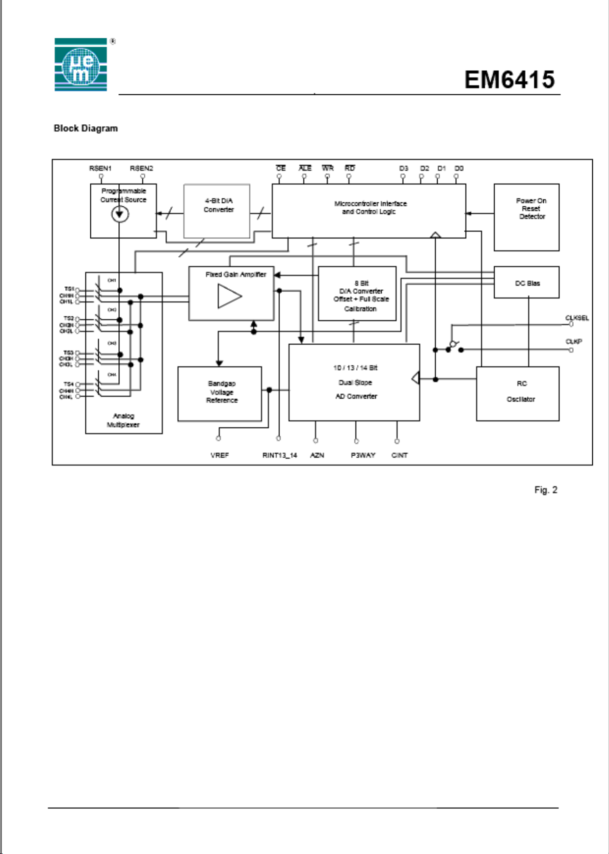
Functional Description
EM6415 comprises a four channel analog multiplexer followed by a fixed gain amplifier followed by the integrator of the dual
slope converter, a bandgap voltage reference, RC oscillator, power on/off detector.
The sensor is supplied directly by a programmable current source.
In order to minimize noise, the analog and digital circuits internal to EM6415 use separate power supplies. These power
buses are brought out to separate pins and should be tied together as close as possible to the device.
In addition, the output of the internal bandgap voltage reference is brought to the pin VREF, which could allow the
connection of an external capacitor to VSS, if the output stability is not enough to resolve 1µV/bit ADC.
Programming Procedure
Nibble organization and Bit order:
Bit
Order
Latch Address (LAD) and Functions
LAD Function Bits D0-D3 WR/RD Note
0 FS fine adjust 0-3 WR
1 FS fine adjust 4-7 WR
2 FS fine adjust 8-11 WR
3 OS rough adjust 0-3 WR
4 OS rough adjust 4-7 WR
5 FS rough adjust 0-3 WR
6 FS rough adjust 4-7 WR
7 Bridge current 0-3 WR
8 ADC status & ADC output AD0, AD1 0-3 RD (note 1)
9 ADC output AD2-AD5 2-5 RD (note 2)
10 ADC output AD6-AD9 & T0-T3 6-9 RD (note 2)
11 ADC output AD10-AD13 & T4-T7 10-13 RD (note 2)
12 ADC resolution (10, 13, 14) 0-3 WR (note 3)
13 Perform ADC conversion (T, R, S, P) 0-3 WR (note 4)
14 Select Sensor-Port (1,2,3,4) & RSEN (1,2) 0-3 WR (note 5)
15 don’t use -
3210
high
→→
low
Note 1: ADC Status & AD0, AD1 (LAD=8)
Bit Function Note
D0 CC Conversion complete = 1
D1 COVFL Conversion overflow = 1
D2 AD0 ADC Bit 0
D3 AD1 ADC Bit 1
Note 2: ADC read out
Latch Address
Buffer Bit
ADC Bits
Sensor AD-14
Sensor AD-13
Sens/Pow AD10
Top of B AD10
3210 3 2 1 0321032
13 12 11 10 9 8 7 6 5 4 3 2 1 0
12 11 10 9 8 7 6 5 4 3 2 1 0 -
9876 5 4 3 210---9876 5 4 3 210----
11 10 9 8
Copyright 2002, EM Microelectronic-Marin SA
7 www.emmicroelectronic.com

Note 3: ADC resolution & frequency select (LAD 12)
Bit Select Function
D1, D0 00 clock 500kHz
01 clock 600kHz
10 clock 700kHz
11 clock 800kHz
D3, D2 00 10 Bit ADC
01 13 Bit ADC
10 13 Bit ADC
11 14 Bit ADC
Note 4: ADC conversion select (LAD=13)
Bit Select Function Note
D1, D0 - don’t use
D3, D2 00 (T) top of sensor bridge with I
01 (R) A/D ramp height (note 7)
10 (S) sensor bridge signal I
11 (P) power supply voltage (note 9)
Note 5: ADC conversion select (LAD=14)
Bit Select Function
D0 0 RSENS1
1 RSENS2
D2, D1 00 Sensor 1 on TS1
01 Sensor 2 on TS2
10 Sensor 3 on TS3
11 Sensor 4 on TS4
D3 - Don’t use
SDRV
/2 (note 6)
SDRV
(note 8)
EM6415
Note 6: Top of sensor bridge, e.g. temperature (ToB – VSSA)
Note 7: Select ramp height if CC=0, ramp height > 1.5V
For lowest ADC jitter, chose ramp height > 1.5V. To do so, run A/D ramp height conversion and read CC
(conversion complete, LAD8, Bit0). Lower the clock frequency until CC=0.
Note 8: Sensor bridge signal, e.g. pressure (CH1L – CH1H)
Note 9: Power supply voltage of EM6415 circuit
Copyright 2002, EM Microelectronic-Marin SA
8 www.emmicroelectronic.com

Integrator
This signal can be seen on pin CINT
EM6415
D
8Bit
A D
OFFSET ROUGH ADJUST
A
8Bit
FS ROUGH ADJUST
min. 1.5V for 14Bit at
3V power supply
0.720V
dV2
dV1
t1 t2 t3
12Bit
D
A
14Bit ADC OUTPUT
FS FINE ADJUST
Fig. 5 Integrator ramp
Time Phase Execution
t1 Autozero phase Set up of integrator starting point
t 2 FS fine adjust Signal integration with preprogrammed counter time length t2
t 3 FS rough adjust De-integration with preprogrammed reference voltage, time length of
t3 = ADC output counts
dV1 is the Offset Rough Adjust
dV2 is the Integrator Ramp Length
Offsets and other system mismatch such as the zero drift of operational amplifiers, long term instabilities or supply
voltage fluctuations are cancelled during the Autozero phase.
Sensitivity and full-scale range adjustments are done during rampup and rampdown of the dual slope integrator.
Copyright 2002, EM Microelectronic-Marin SA
9 www.emmicroelectronic.com

EM6415
Pad Description & Pin Assignment in SSOP36
PIN Nr Name I/O Description
10 TS1 Top of sensor1 bridge connection pin
11 CH1H Sensor1 channel high signal in
12 CH1L Sensor1 channel low signal in
13 TS2 Top of sensor2 bridge connection pin
14 CH2H Sensor2 channel high signal in
15 CH2L Sensor2 channel low signal in
16 TS3 Top of sensor3 bridge connection pin
17 CH3H Sensor3 channel high signal in
18 CH3L Sensor3 channel low signal in
19 TS4 Top of sensor4 bridge connection pin
20 CH4H Sensor4 channel high signal in
21 CH4L Sensor4 channel low signal in
2 D0P I/O Microprocessor Port Data 0
1 D1P I/O Microprocessor Port Data 1
36 D2P I/O Microprocessor Port Data 2
35 D3P I/O Microprocessor Port Data 3
31
32
33
34
22 CINT Connection to integrator capacitor
23 AZN Connection to auto-zero capacitor
24 P3WAY 3 way connection for integrator
25 RINT13_14 Connection of resistor for integrator
26 RINT10 Connection of resistor for integrator when 10 bit conversion used
8 RSEN1 Resistor to select sensor bridge1 maximum drive current
9 RSEN2 Resistor to select sensor bridge2 maximum drive current
3 CLKP I External clock input
5 CLKSEL I Internal/external clock select
6 VDDD Positive supply voltage of digital part
7 VDDA Positive supply voltage of analog part
29 VSSA Negative supply voltage of analog part
30 VSSD Negative supply voltage of digital part
27 VREF O Reference voltage
4, 28 NC Not connected
RD
ALE
CE
WR
I Read strobe for BUS read (active low)
I Address latch enable (active low)
I Chip enable (active low)
I Write strobe for BUS write (active low)
I: Input O: Output
Copyright 2002, EM Microelectronic-Marin SA
10 www.emmicroelectronic.com

Package Information
SSOP36 – 300 mils
EM6415
Symbol Common dimensions (inches) Note Symbol Common dimensions (mm) Note
Min Nom Max Min. Nom Max
A 0.097 0.101 0.104 A 2.46 2.56 2.64
A1 0.0050 0.009 0.0115 A1 0.127 0.22 0.29
A2 0.090 0.092 0.094 A2 2.29 2.34 2.39
B 0.012 0.014 0.017 B 0.31 0.36 0.43
C 0.0091 0.010 0.0125 C 0.23 0.25 0.32
D 0.602 0.607 0.612 D 15.29 15.42 15.54
E 0.292 0.296 0.299 E 7.42 7.52 7.59
e 0.0315
BSC
H 0.400 0.406 0.410 H 10.16 10.31 10.41
h 0.010 0.013 0.016 h 0.25 0.33 0.41
L 0.024 0.032 0.040 L 0.61 0.81 1.02
X 0.085 0.093 0.100 X 2.16 2.36 2.54
α
Copyright 2002, EM Microelectronic-Marin SA
0° 5° 8°
e0.80
BSC
α
11 www.emmicroelectronic.com
0° 5° 8°

EM6415
Ordering Information
The EM6415 has metal mask options for the Gain of the Input Amplifier (between 1 and 150 max) and for the Offset Adjust
Range. Contact EM Microelectronic for availability of different options not shown in table below. Please make sure to order
the exact Part Number when ordering.
Part Number Version
EM6415V1WS11
EM6415V1SS36A
EM6415V1SS36B
EM6415V2WS11
EM6415V2SS36A
EM6415V2SS36B
EM6415V3WS11
EM6415V3SS36A
EM6415V3SS36B
EM6415V%WS11
EM6415V%SS36A
EM6415V%SS36B
V1 5 Separate Registers -40mV to +40mV 36-pin SSOP, Stick
V2 5 Common Registers -40mV to +40mV 36-pin SSOP, Stick
V3 150 Separate Registers -40mV to +40mV 36-pin SSOP, Stick
V% custom custom custom 36-pin SSOP, Stick
Input
Amplifier
Gain
OS/FS Rough Adjust
(note 1)
for each sensor 36 pin SSOP, Tape & Reel
for the 4 sensors 36 pin SSOP, Tape & Reel
for each sensor 36 pin SSOP, Tape & Reel
Offset Adjust
Range
Delivery Form
Sawn wafer, 11 mils thickness
Sawn wafer, 11 mils thickness
Sawn wafer, 11 mils thickness
Sawn wafer, 11 mils thickness
36 pin SSOP, Tape & Reel
Note 1: LAD 3, 4, 5, 6
For die size information and pad location diagram, please contact EM Microelectronic-Marin SA.
EM Microelectronic-Marin SA cannot assume responsibility for use of any circuitry described other than circuitry
entirely embodied in an EM Microelectronic-Marin SA product. EM Microelectronic-Marin SA reserves the right to
change the circuitry and specifications without notice at any time. You are strongly urged to ensure that the
information given has not been superseded by a more up-to-date version.
© EM Microelectronic-Marin SA, 11/02, Rev. B
Copyright 2002, EM Microelectronic-Marin SA
12 www.emmicroelectronic.com
 Loading...