


查询EM6325AX-1.3供应商
EM MICROELECTRONIC - MARIN SA
Reset Circuit with Manual Reset
Description
The EM6325 is an ultra-low current reset circuit available in a
large variety of configurations and very small packages for
maximum flexibility in all end-applications up to 125°C and
using power supplies between 1.5V and 5.5V.
This circuit monitors the supply voltage of any electronic
system, and generates the appropriate reset signal after a
fixed reset timeout period. The threshold defines the
minimum allowed voltage which guarantees the good
functionality of the system. When VDD rises above VTH, the
output remains active for an additional delay time. This
allows the system to stabilize before getting fully active.
This circuit features a Manual Reset: an input that asserts
reset when pulled low (MR with internal pull-up).
Small SC70-4L, SC70-5L and SOT23-5L packages as well
as ultra-low supply current of 2.9μA make the EM6325 an
ideal choice for portable and battery-operated devices.
Typical Application
V
DD
V
DD
RESET
EM6325
RESET
MR
GND
GND
R
for open-drain version only
*
EXT
Block Diagram
V
DD
Voltage
Reference
MR
GND
Filter
Pin Description
Pin
SOT23-5L / SC70-5L SC70-4L
1 2
2 1 GND Ground
3 2 RESET
4 3
5 4 VDD Supply Voltage (5.5V max.)
*
+
-
Name Function
RESET
MR
V
DD
RESET
MPU, DSP
RESET
GND
Oscillator
Reset
Logic
Active-low
then goes high after all reset conditions are deasserted or after
to high
Active-high RESET output. RESET remains high for the reset timeout period and
then goes low after all reset conditions are deasserted or after
high
Manual Reset input with an internal pull-up 15k
long as
CMOS output or shorted to ground with a switch
RESET
RESET
RESET output. RESET remains low for the reset timeout period and
MR is low and for t
EM6325
Features
Manual reset function
200ms reset timeout period (1.6ms, 25ms, 1600ms on
request)
Ultra-low supply current of 2.9μA (V
Operating temperature range: -40°C to +125°C
±1.5% reset threshold accuracy
11 reset threshold voltages V
TH
2.93V, 2.63V, 2.2V, 1.8V, 1.66V, 1.57V, 1.38V, 1.31V
3 reset output options:
Active-low
Active-low
Active-high
Immune to short negative V
RESET push-pull
RESET open-drain
RESET push-pull
transients
DD
Guaranteed Reset valid down to 0.9V
Threshold hysteresis: 2.1% of V
Very small SOT23-5L, SC70-5L and SC70-4L
Applications
Computers
Servers and workstations
Modems
Wireless communication
Metering
Playstations
PDA , Webpad
Automotive systems
Pin Configuration (top view)
RESET
GND
RESET
push-pull
1
2
3
push-pull / open-drain
SOT23-5 / SC70-5
top view
after MR returns high. MR can be driven with a
POR
V
5
DD
GND
MR
RESET
(RESET)
4
Ω resistor. Reset remains active as
=3.3V)
DD
: 4.63V, 4.4V, 3.08V,
TH
1
2
SC70-4
top view
MR goes from low
MR
V
4
DD
MR
3
goes from low to
Copyright © 2005, EM Microelectronic-Marin SA
1 www.emmicroelectronic.com

R
[
]
p
g
g
g
p
p
p
Ordering Information
EM6325 -
EM6325
+C X SP5B 2.9
Delay (t
C = 200ms
A = 1.6ms D = 1600ms
Reset Output Type:
X = Active-low /RES push-pull 1.3 = 1.31V 2.6 = 2.63V
Active-high RES push-pull 1.4 = 1.38V 2.9 = 2.93V
Y = Active-low /RES o
Active-hi
Z = Active-hi
Packa
SP5B = SOT23-5, Ta
SC5B = SC70-5, Ta
SC4B = SC70-4, Ta
):
PO
h RES push-pull 1.7 = 1.66V 4.4 = 4.40V
h RES push-pull 1.8 = 1.80V 4.6 = 4.63V
e:
B = 25ms + = lead-free/green mold compliant
en-drain 1.6 = 1.57V 3.1 = 3.08V
e&Reel 3000 pcs
e&Reel 3000 pcs
e&Reel 3000 pcs
RoHS Compliance:
blank
= leaded
Reset Threshold Voltage (V
2.2 = 2.20V
):
TH
Top Marking
Package top marking below is for most parts in leaded package (first letter is “A”). For lead-free/green mold (RoHS) parts,
the first letter of top marking begins with letter “B” instead of letter “A”. The underscore "_ _" refers to the four-letter code for
the package (eg. SP5B, SC4B, …).
Part Number
EM6325AX__-1.3 ANAA EM6325BX__-1.3 ANBA EM6325CX__-1.3 ANCA EM6325DX__-1.3 ANDA
EM6325AX__-1.4 ANAB EM6325BX__-1.4 ANBB EM6325CX__-1.4 ANCB EM6325DX__-1.4 ANDB
EM6325AX__-1.6 ANAC EM6325BX__-1.6 ANBC EM6325CX__-1.6 ANCC EM6325DX__-1.6 ANDC
EM6325AX__-1.7 ANAD EM6325BX__-1.7 ANBD EM6325CX__-1.7 ANCD EM6325DX__-1.7 ANDD
EM6325AX__-1.8 ANAE EM6325BX__-1.8 ANBE EM6325CX__-1.8 ANCE EM6325DX__-1.8 ANDE
EM6325AX__-2.2 ANAF EM6325BX__-2.2 ANBF EM6325CX__-2.2 ANCF EM6325DX__-2.2 ANDF
EM6325AX__-2.6 ANAG EM6325BX__-2.6 ANBG EM6325CX__-2.6 ANCG EM6325DX__-2.6 ANDG
EM6325AX__-2.9 ANAH EM6325BX__-2.9 ANBH EM6325CX__-2.9 ANCH EM6325DX__-2.9 ANDH
EM6325AX__-3.1 ANAJ EM6325BX__-3.1 ANBJ EM6325CX__-3.1 ANCJ EM6325DX__-3.1 ANDJ
EM6325AX__-4.4 ANAK EM6325BX__-4.4 ANBK EM6325CX__-4.4 ANCK EM6325DX__-4.4 ANDK
EM6325AX__-4.6 ANAL EM6325BX__-4.6 ANBL EM6325CX__-4.6 ANCL EM6325DX__-4.6 ANDL
EM6325AY__-1.3 ANAM EM6325BY__-1.3 ANBM EM6325CY__-1.3 ANCM EM6325DY__-1.3 ANDM
EM6325AY__-1.4 ANAN EM6325BY__-1.4 ANBN EM6325CY__-1.4 ANCN EM6325DY__-1.4 ANDN
EM6325AY__-1.6 ANAP EM6325BY__-1.6 ANBP EM6325CY__-1.6 ANCP EM6325DY__-1.6 ANDP
EM6325AY__-1.7 ANAQ EM6325BY__-1.7 ANBQ EM6325CY__-1.7 ANCQ EM6325DY__-1.7 ANDQ
EM6325AY__-1.8 ANAR EM6325BY__-1.8 ANBR EM6325CY__-1.8 ANCR EM6325DY__-1.8 ANDR
EM6325AY__-2.2 ANAS EM6325BY__-2.2 ANBS EM6325CY__-2.2 ANCS EM6325DY__-2.2 ANDS
EM6325AY__-2.6 ANAT EM6325BY__-2.6 ANBT EM6325CY__-2.6 ANCT EM6325DY__-2.6 ANDT
EM6325AY__-2.9 ANAU EM6325BY__-2.9 ANBU EM6325CY__-2.9 ANCU EM6325DY__-2.9 ANDU
EM6325AY__-3.1 ANAV EM6325BY__-3.1 ANBV EM6325CY__-3.1 ANCV EM6325DY__-3.1 ANDV
EM6325AY__-4.4 ANAW EM6325BY__-4.4 ANBW EM6325CY__-4.4 ANCW EM6325DY__-4.4 ANDW
EM6325AY__-4.6 ANAX EM6325BY__-4.6 ANBX EM6325CY__-4.6 ANCX EM6325DY__-4.6 ANDX
Top
Marking
Part Number
Top
Marking
Part Number
Top
Marking
Part Number
Top
Marking
Standard Versions, Samples
Sample stock is generally held on standard versions (below) only. Non standard versions have a 30,000 pieces minimum
order quantity. Please contact factory for other versions not shown here and for availability of non standard versions.
EM6325AXSC4B-2.9
EM6325CXSC5B-2.9
EM6325CXSP5B-1.3
EM6325CXSP5B-2.6
EM6325CXSP5B-2.9
EM6325CXSP5B-3.1
EM6325CYSP5B-2.9
EM6325CYSP5B-4.6
EM6325DXSC4B-2.6
EM6325CXSP5B-4.6
Copyright © 2005, EM Microelectronic-Marin SA
2 www.emmicroelectronic.com

n
Absolute Maximum Ratings
Parameter Symbol Conditions
Voltage at VDD to GND VDD -0.3V to +6V
Minimum voltage at any signal pin V
Maximum voltage at any signal pi
Electrostatic discharge max. to
MIL-STD-883C method 3015.7
with ref. to V
Max. soldering conditions T
Storage Temperature Range T
Stresses above these listed maximum ratings may
cause permanent damages to the device. Exposure
beyond specified operating conditions may affect device
reliability or cause malfunction.
Handling Procedures
This device has built-in protection against high static
GND - 0.3V
MIN
V
VDD + 0.3V
MAX
V
2000V
SS
ESD
250°C x 10s
MAX
-65°C to +150°C
STG
voltages or electric fields; however, anti-static
precautions must be taken as for any other CMOS
component. Unless otherwise specified, proper
operation can only occur when all terminal voltages are
kept within the voltage range. Unused inputs must
always be tied to a defined logic voltage level.
Operating Conditions
Parameter Symbol Min Max Unit
Supply voltage VDD 0.9 5.5 V
Operating Temperature TA -40 +125 °C
EM6325
Electrical Characteristics
Unless otherwise specified: VDD= 0.9V to 5.5V, T
Parameter Symbol Conditions Min Typ Max Unit
Supply current (note 2) IDD
Threshold voltage
(note 3)
Threshold hysteresis V
V
TH
T
HYS
Note 1: Production tested at +25°C only. Over temperature limits are guaranteed by design, not production tested.
Note 3: Threshold voltage is specified for V
=-40°C to +125°C (note 1).
A
VDD=1.5V
VDD=3.3V
=5.0V
V
DD
+25°C - 4.6
-40°C to +125°C +25°C - 5.5
-40°C to +125°C +25°C - 6.3
-40°C to +125°C +25°C 1.290 1.330
EM6325 – 1.3
-40°C to +85°C 1.245 1.382
-40°C to +125°C 1.221
+25°C 1.359 1.401
EM6325 – 1.4
-40°C to +85°C 1.311 1.456
-40°C to +125°C 1.286
+25°C 1.546 1.594
EM6325 – 1.6
-40°C to +85°C 1.492 1.656
-40°C to +125°C 1.463
+25°C 1.635 1.685
EM6325 – 1.7
-40°C to +85°C 1.577 1.751
-40°C to +125°C 1.547
+25°C 1.773 1.827
EM6325 – 1.8
-40°C to +85°C 1.710 1.899
-40°C to +125°C 1.678
+25°C 2.167 2.233
EM6325 – 2.2
-40°C to +85°C 2.090 2.321
-40°C to +125°C 2.050
+25°C 2.591 2.669
EM6325 – 2.6
-40°C to +85°C 2.499 2.775
-40°C to +125°C 2.451
+25°C 2.886 2.974
EM6325 – 2.9
-40°C to +85°C 2.784 3.091
-40°C to +125°C 2.731
+25°C 3.034 3.126
EM6325 – 3.1
-40°C to +85°C 2.926 3.249
-40°C to +125°C 2.871
+25°C 4.334 4.466
EM6325 – 4.4
-40°C to +85°C 4.180 4.642
-40°C to +125°C 4.101
+25°C 4.561 4.699
EM6325 – 4.6
-40°C to +85°C 4.399 4.885
-40°C to +125°C 4.315
=+25°C -
A
falling.
DD
1.31
1.38
1.57
1.66
1.80
2.20
2.63
2.93
3.08
4.40
4.63
2.1%
2.3
2.9
3.4
•V
7
8.3
μA
9.6
1.387
1.461
1.663
1.758
1.906
V
2.330
2.785
3.103
3.262
4.660
4.903
- V
TH
Copyright © 2005, EM Microelectronic-Marin SA
3 www.emmicroelectronic.com

Electrical Characteristics
(continued)
EM6325
Unless otherwise specified: V
= 0.9V to 5.5V, T
DD
=-40°C to +125° C (note 1).
A
Parameter Symbol Conditions Min Typ Max Unit
EM6325C 155 200 224
Reset timeout period t
POR
VDD from 0V to V
T
= +25°C
A
TH (typ)
+15%
(note 2 and 4)
EM6325A 0.7 1.6 3.8
EM6325B 19.4 25 28
ms
EM6325D 1240 1600 1792
Propagation delay time
to RESET (RESET) delay
V
DD
Open-drain RESET output
Voltage
Push-pull RESET / RESET
Output voltage
Output leakage current I
MANUAL RESET (MR )
MR Input low
MR Input high
V
V
MR to Reset delay
Pulse width at MR (note 5)
MR Internal Pull-up resistor
t
P
V
OL
VOL
V
OH
Only for EM6325_Y (open-drain) - - 0.5
LEAK
low 0.3•V
MRT
high 0.7•VDD V
MRT
t
0.3
MD
t
PMD
R
T
MR
V
drops from V
DD
(note 2). T
= +25°C
A
VDD>1V
VDD>2.5V IOL=1.5mA - - 0.3
V
>5V IOL=3mA - - 0.35
DD
VDD>1V
TH (typ)
+0.2V to V
I
=100μA
OL
I
=100μA
OL
TH (typ)
-0.2V
2 130 255
μs
- - 0.3
V
- - 0.3
VDD>2.5V IOL=1.5mA - - 0.3
V
>5V IOL=3mA - - 0.35
DD
VDD>1V
I
=-30μA
OH
0.8 - -
V
VDD>2.5V IOH=-1.5mA 2 - -
V
>5V IOH=-3mA 4 - -
DD
μA
V
DD
T
= +25°C
A
1
=-40°C to +125°C 4.8 15 31
A
μs
μs
k
Ω
Note 1: Production tested at +25°C only. Over temperature limits are guaranteed by design, not production tested.
Note 2:
Note 4: Standard version for t
RESET (RESET) open.
is 200ms (typ), available at all times. Other option (1.6ms, 25ms, 1600ms) are available
POR
by mask option and upon minimum order quantity. Please contact EM sales.
Note 5: Pulse width must be greater than 1μs to ensure the
RESET
(RESET) to go active.
Copyright © 2005, EM Microelectronic-Marin SA
4 www.emmicroelectronic.com
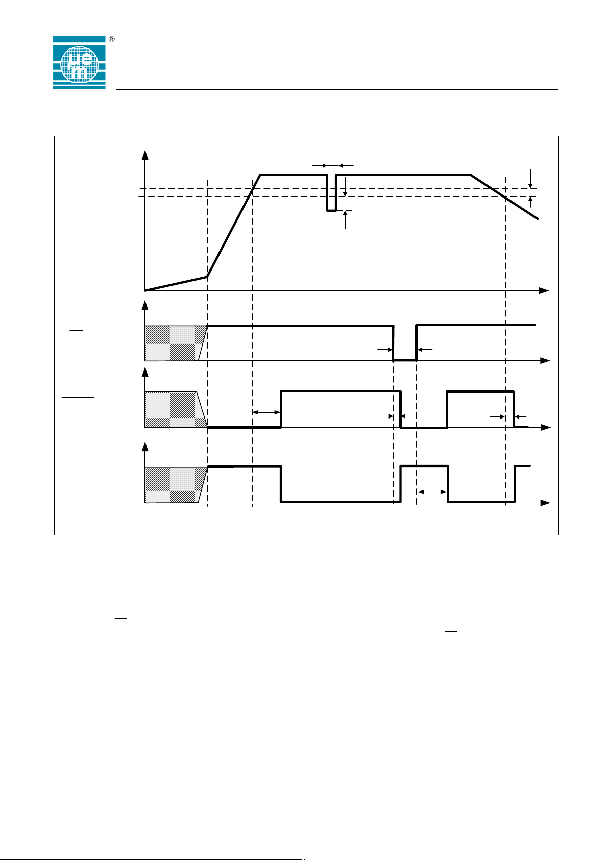
Timing Waveforms
V
DD
V
TH
0.8V
logic "1"
MR
t
SEN
Overdrive
t
PMD
EM6325
V
HYS
t
logic "0"
logic "1"
RESET
t
POR
t
MD
logic "0"
logic "1"
RESET
t
POR
logic "0"
Note 6: t
Note 7: Overdrive = V
Manual Reset Input
A logic low on
it returns high. MR has an internal 15kΩ pull-up resistor, so it can be left open if unused. This input can be driven with
CMOS logic levels or with open-drain outputs. Connect a normally open momentary switch from
manual-reset function; debounce circuitry is integrated. If
environment, connect a 0.1μF capacitor from MR to VSS to provide additional noise immunity (stronger external additional
pull-up resistor can also be added).
= Maximum Transient Duration. Please refer to figure on the next page.
SEN
MR asserts a reset. Reset remains asserted while MR is low, and for t
-VDD. Please refer to figure on the next page.
TH
MR is driven from long cable or the device is used in a noisy
(200ms nominal for EM6325C) after
POR
MR
to VSS to create a
t
t
P
t
t
Copyright © 2005, EM Microelectronic-Marin SA
5 www.emmicroelectronic.com

V
Typical Operating Characteristics
(Typical values are at TA=+25°C unless otherwise noted, MR ,
RESET
and RESET open.)
EM6325
7
6
[ uA ]
5
4
V
5 . 0 V
DD
3
V
1 . 5 V
2
DD
1
0
-50 -25 0 25 50 75 100 125
[ °C ]
I
vs. Temperature Propagation Time tP vs. Temperature
DD
200%
175%
150%
t
POR (°C)
t
POR (25°C)
125%
100%
75%
50%
25%
0%
-50 -25 0 25 50 75 100 125
[ °C ]
V
3 . 3
DD
250
200
[ us ]
150
100
50
0
-50 -25 0 25 50 75 100 125
[ °C ]
400
350
300
300
250
[ us ]
200
150
Reset occurs
above this line
100
50
0
1 10 100 1000
[ mV ]
Reset Timeout Period t
(normalized with respect to t
vs. Temperature Maximum Transient Duration t
POR
) vs. Overdrive VTH-VDD
POR 25°C
SEN
8%
6%
4%
2%
0%
-2%
-4%
-6%
-8%
-50 -25 0 25 50 75 100 125
[°C]
Threshold Voltage Variation vs. Temperature (normalized)
Copyright © 2005, EM Microelectronic-Marin SA
6 www.emmicroelectronic.com

Package Information
EM6325
HE
PIN 1
D
A2
A1
SOT23-5L
A
C
b
E1
L
E
e
e1
D
E
e
b
e
SC70-5L
Q1
c
SYM BOL MIN TYP MAX
A 0.90 1.30 1.45
A1 0.05 0.08 0.15
A2 0.90 1.15 1.30
b0.35 0.50
C0.08 0.20
D 2.80 2.90 3.00
E 2.60 2.80 3.00
E1 1.50 1.75
e0.95
e1 1.90
L 0.45
Dimensions are in mm
SYMBOL MIN MAX
e
L
D1.802.20
b0.150.30
E1.151.35
HE 1.80 2.40
Q1 0.10 0.40
A2 0.80 1.00
A1 0.00 0.10
A0.801.10
c0.100.18
L0.100.30
0.65 BSC
A2
Copyright © 2005, EM Microelectronic-Marin SA
A
A1
NOTE:
y All dimensions are in millimeters
y Dimensions are inclusive of plating
y Dimensions are exclusive of mold flash & metal burr
y All specifications comply to EIAJ SC70
7 www.emmicroelectronic.com
EM6325
D
e
e
SC70-4L
L
SYMBOL MIN MAX
e
e1
0.65 BSC
0.5 BSC
D1.802.20
b0.150.30
HE
E
b1 0.575 0.70
E1.151.35
HE 1.80 2.40
PIN 1
e1
Q1 0.10 0.40
A2 0.80 1.00
A1 0.00 0.10
Q1
c
A0.801.10
c0.100.18
L0.100.30
A2
b
b1
NOTE:
y All dimensions are in millimeters
y Dimensions are inclusive of plating
A
y Dimensions are exclusive of mold flash & metal burr
y All specifications comply to EIAJ SC70
y Even though the width of pin 2 on SC70-4L is slightly larger than on so-
A1
called 4-pin SC-82AB, the footprint of SC70-4L package is compatible
with the footprint of SC-82AB package from other suppliers, and thus
suitable for pin-to-pin replacement. Please check footprint on PCB.
Traceability for small packages
Due to the limited space on the package surface, the bottom marking contains a limited number of characters that provide only partial
information for lot traceability. Full information for complete traceability is however provided on the packing labels of the product at
delivery from EM. It is highly recommended that the customer insures full lot traceability of EM product in his final product.
EM Microelectronic-Marin SA (EM) makes no warranty for the use of its products, other than those expressly contained in the Company's
standard warranty which is detailed in EM's General Terms of Sale located on the Company's web site. EM assumes no responsibility for
any errors which may appear in this document, reserves the right to change devices or specifications detailed herein at any time without
notice, and does not make any commitment to update the information contained herein. No licenses to patents or other intellectual
property of EM are granted in connection with the sale of EM products, expressly or by implications. EM's products are not authorized for
use as components in life support devices or systems.
Product qualification is performed according to internal EM quality standards for industrial products. For any special requirement (eg. automotive grade) please
contact EM Microelectronic-Marin S.A.
© EM Microelectronic-Marin SA, 05/05, Rev. I
Copyright © 2005, EM Microelectronic-Marin SA
8 www.emmicroelectronic.com

WWW.ALLDATASHEET.COM
Copyright © Each Manufacturing Company.
All Datasheets cannot be modified without permission.
This datasheet has been download from :
www.AllDataSheet.com
100% Free DataSheet Search Site.
Free Download.
No Register.
Fast Search System.
www.AllDataSheet.com
 Loading...