

EMLSI EM641FT8V Service Manual
EM641FT8V Series
Low Power, 512Kx8 SRAM
Document Title
512K x8 bit Low Power Full CMOS Static RAM
Revision History
Revision No. History Draft Date Remark
0.0 Initial Draft
0.1 0.1 Revision
I
Current from 1.5uA to 7uA
DR
tOE from 25nsec to 30nsec with 55ns part
Nov. 20, 2007 Preliminary
Dec. 5, 2007
Emerging Memory & Logic Solutions Inc.
4F Korea Construction Financial Cooperative B/D, 301-1 Yeon-Dong, Jeju-Si, Jeju-Do, Rep.of Korea Zip Code : 690-719
Tel : +82-64-740-1712 Fax : +82-64-740-1749~1750 / Homepage : www.emlsi.com
The attached data sheets are provided by EMLSI reserve the right to change the specifications and products. EMLSI will answer to your
questions about device. If you have any questions, please contact the EMLSI office.
1
512K x8 Bit Low Power CMOS Static RAM
FEATURES
- Very high speed : 45ns
- Process Technology : 0.15um Full CMOS
- Organization : 512K x8
- Power Supply Voltage
=> EM641FT8V : 4.5V~5.5V
- Low Data Retention Voltage : 1.5V (MIN)
- Three state output and TTL Compatible
- Packaged product designed for 45/55/70ns
- Package Type: 32L-SOP
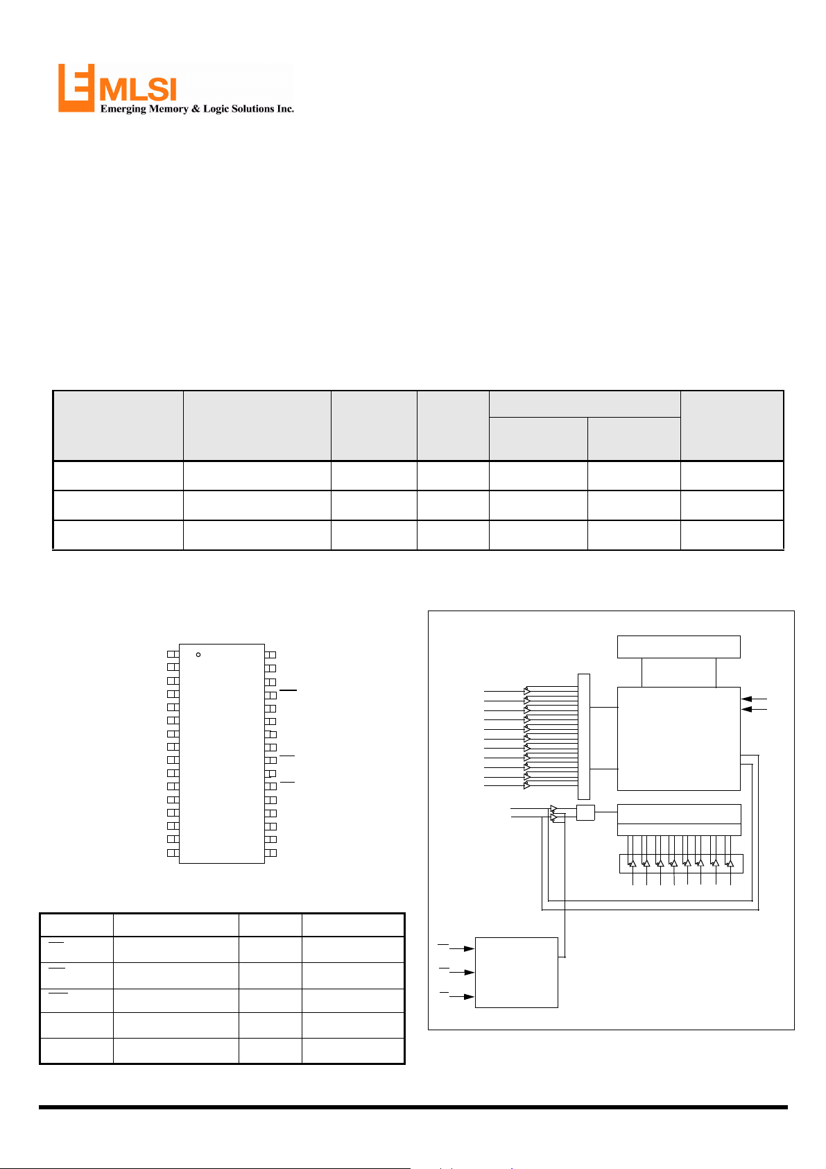
PRODUCT FAMILY
Product
Family
Operating
Temperature
Vcc Range Speed
EM641FT8V Series
Low Power, 512Kx8 SRAM
GENERAL DESCRIPTION
The EM641FT8V is fabricated by EMLSI’s advanced full
CMOS process technology. The families support industrial
temperature range and Chip Scale Package for user flexibility of system design. The families also supports low data
retention voltage for battery back-up operation with low
data retention current.
The EM641FT8V is available in KGD, JEDEC standard 32
pin 450mil Plastic SOP package.
Power Dissipation
Standby
(I
, Typ.)
SB1
Operating
(I
.Max)
CC1
PKG Type
EM641FT8V-45LF
EM641FT8V-55LF
EM641FT8V-70LF
PIN DESCRIPTION
A
18
A
16
A
14
A
12
A
7
A
6
A
5
A
4
A
3
A
2
A
1
A
0
I/O
0
I/O
1
I/O
2
V
SS
Industrial (-40 ~ 85oC)
Industrial (-40 ~ 85oC)
Industrial (-40 ~ 85oC)
EM641FT8V
1
2
3
4
5
6
7
8
9
10
11
12
13
14
15
16
32
31
30
29
28
27
26
25
24
23
22
21
20
19
18
17
V
A
A
WE
A
A
A
A
OE
A
CS
I/O
I/O
I/O
I/O
I/O
CC
15
17
13
8
9
11
10
7
6
5
4
3
4.5V~5.5V 45ns 1.5 µA 7mA 32-SOP
4.5V~5.5V 55ns 1.5 µA 7mA 32-SOP
4.5V~5.5V 70ns 1.5 µA 7mA 32-SOP
FUNCTIONAL BLOCK DIAGRAM
Pre-charge Circuit
A
0
A
1
A
2
A
3
A
4
A
5
A
6
A
7
A
8
A
9
A
10
I/O0 ~ I/O
Row Select
Data
7
Cont
Memory Array
512K x 8
I/O Circuit
Column Select
V
CC
V
SS
Name Function Name Function
CS Chip select input
OE Output Enable input
V
CC
V
SS
Power Supply
Ground
WE Write Enable input
A0~A
I/O
0
18
~I/O
Address Inputs
Data Inputs/Outputs
7
A
A
A
A
A
12
11
WE
OE
CS
Control Logic
A
A
A
15
14
13
16
17
18
2

ABSOLUTE MAXIMUM RATINGS
Parameter Symbol Minimum Unit
EM641FT8V Series
Low Power, 512Kx8 SRAM
Voltage on Any Pin Relative to V
Voltage on Vcc supply relative to V
SS
SS
Power Dissipation P
Operating Temperature T
Note : Stresses greater than those listed above “Absolute Maximum Ratings” may cause permanent damage to the device.
Functional operation should be restricted to recommended operating condition. Exposure to absolute maximum rating conditions for extended periods may affect reliability.
VIN, V
V
CC
D
A
OUT
-0.5 to 6.0V V
-0.5 to 6.0V V
1.0 W
-40 to 85
o
C
FUNCTIONAL DESCRIPTION
CS OE WE I/O
H X X High-Z Deselected/ Power down Stand by
L L H Data Out Read Active
L X L Data In Write Active
L H H High-Z Selected, Output Disabled Active
Note : X means don’t care. (Must be low or high state)
0-7
Mode Power
3
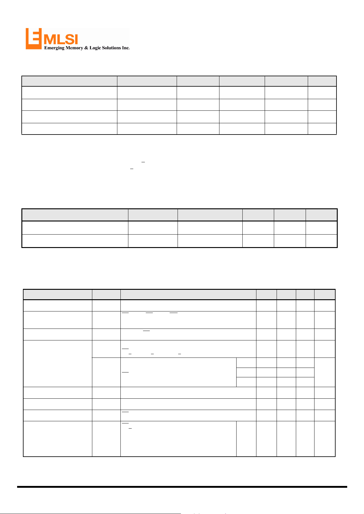
RECOMMENDED DC OPERATING CONDITIONS
Parameter Symbol Min Typ Max Unit
Supply voltage
Ground V
Input high voltage V
Input low voltage V
2)
V
CC
SS
IH
IL
1)
4.5 - 5.5
0 0 0
2.2 - VCC + 0.5
4)
-0.5
Notes :
1. TA= -40 to 85oC, otherwise specified
2. Overshoot: VCC +1.0 V in case of pulse width < 20ns
3. Undershoot: -1.0 V in case of pulse width < 20ns
4. Overshoot and undershoot are sampled, not 100% tested.
CAPACITANCE (f =1MHz, TA=25oC)
Item Symbol Test Condition Min Max Unit
EM641FT8V Series
Low Power, 512Kx8 SRAM
V
V
3)
- 0.6 V
V
Input capacitance C
Input/Ouput capacitance C
IN
IO
VIN=0V - 8 pF
VIO=0V - 10 pF
Note : Capacitance is sampled, not 100% tested.
DC ELECTRICAL CHARACTERISTICS (TA = -40oC to +85oC)
Parameter Symbol Test Conditions Min Typ Max Unit
I
Input leakage current
Output leakage current
Operating power supply
Average operating current
Output low voltage
Output high voltage
Standby Current (TTL)
Standby Current (CMOS)
I
I
I
CC1
I
CC2
V
V
I
I
SB1
VIN=VSS to V
LI
CS=VIH or OE=V
LO
VIO=VSS to V
IIO=0mA, CS=VIL, VIN=VIH or V
CC
Cycle time=1µs, 100% duty, IIO=0mA,
CS<0.2V, VIN<0.2V or VIN>VCC-0.2V
Cycle time = Min, IIO=0mA, 100% duty,
CS=VIL, VIN=VIL or V
IOL = 2.1mA
OL
IOH = -1.0mA
OH
CS=VIH, Other inputs=VIH or V
SB
CS>VCC-0.2V
Other inputs = 0~VCC
(Typ. condition : VCC=5V @ 25oC)
(Max. condition : VCC=5.5V @ 85oC)
CC
CC
or WE=V
IH
IH
IL
IL
IL
-1 - 1 uA
-1 - 1 uA
- - 5 mA
- - 7 mA
45ns - - 65
70ns - - 45
- - 0.4 V
2.4 - - V
- - 1 mA
LF -
1.5
1)
20 uA
mA55ns - - 55
NOTES :
1.Typical values are measured at Vcc=5V, TA=25oC and not 100% tested.
4
 Loading...