


merging Memory & Logic Solutions Inc.merging Memory & Logic Solutions Inc.
Document Title
256K x8 bit Super Low Power and Low Voltage Full CMOS Static RAM
Revision History
Revision No. History Draft Date Remark
0.0 Initial Draft May 31 , 2004
Low Power, 256Kx8 SRAM
EM620FV8AT Series
0.1 1’st Revision I
( @55ns product : 25mA -> 30mA )
0.2 2’nd Revision I
I
I
I
value change ( @70ns product : 20mA -> 25mA )
CC2
Max. value changed from 5uA to 15uA.
SB1
Typ. value deleted.
SB1
Max. value changed to 5uA.
DR
Typ. value deleted.
DR
Dec 14 , 2004
Jan 4 , 2005
Emerging Memory & Logic Solutions Inc.
4F Korea Construction Financial Cooperative B/D, 301-1 Yeon-Dong, Jeju-Si, Jeju-Do, Rep.of Korea Zip Code : 690-719
Tel : +82-64-740-1712 Fax : +82-64-740-1749~1750 / Homepage : www.emlsi.com
The attached datasheets are provided by EMLSI reserve the right to change the specifications and products. EMLSI will answer to your
questions about device. If you have any questions, please contact the EMLSI office.
1
Rev 0.2
merging Memory & Logic Solutions Inc.merging Memory & Logic Solutions Inc.
EM620FV8AT Series
Low Power, 256Kx8 SRAM
FEATURES
• Process Technology : 0.15µm Full CMOS
• Organization : 256K x 8 bit
• Power Supply Voltage : 2.7V ~ 3.6V
• Low Data Retention Voltage : 1.5V(Min)
• Three state output and TTL Compatible
• Package Type : 32-TSOP1
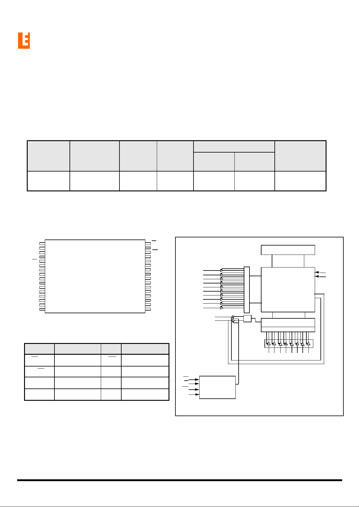
PRODUCT FAMILY
Product
Family
EM620FV8AT
1. The parameter is measured with 30pF test load.
Operating
Temperature
Industrial
(-40 ~ 85oC)
Vcc
Range
2.7V~3.6V
GENERAL DESCRIPTION
The EM620FV8AT families are fabricated by EMLSI’s
advanced full CMOS process technology. The families
support industrial temperature range and Chip Scale
Package for user flexibility of system design. The families also supports low data retention voltage for battery
back-up operation with low data retention current.
Power Dissipation
Speed
1)
55
/ 70ns 15 µA
Standby
(I
, Max)
SB1
Operating
(I
.Max)
CC1
3 mA 32 TSOP1
PKG Type
FUNCTIONAL BLOCK DIAGRAMPIN DESCRIPTION
A11
A9
A8
A13
WE
CS2
A15
VCC
A17
A16
A14
A12
A7
A6
A5
A4
1
2
3
4
5
6
7
8
9
10
11
12
13
14
15
16
32 - TSOP
Type1 - Forward
32
OE
31
A10
30
CS1
29
IO8
28
IO7
27
IO6
26
IO5
25
IO4
24
VSS
23
I/O3
22
I/O2
21
I/O1
20
A0
19
A1
18
A2
17
A3
Name Function Name Function
CS1,CS2 Chip select inputs WE Write Enable input
OE Output Enable input Vcc Power Supply
A0~A17 Address Inputs Vss Ground
I/O1~I/O8 Data Inputs/outputs NC No Connection
Pre-charge Circuit
A
0
A
1
A
2
A
3
A
4
A
5
A
6
A
7
A
8
A
9
I/O1 ~ I/O8
Cont
Data
Memory Array
Row Select
1024 x 2048
I/O Circuit
V
CC
V
SS
Column Select
A10A
11A12A13A14A15
WE
OE
CS1
CS2
Control Logic
A
A
16
17
2
Rev 0.2
merging Memory & Logic Solutions Inc.merging Memory & Logic Solutions Inc.
ABSOLUTE MAXIMUM RATINGS *
Parameter Symbol Ratings Unit
EM620FV8AT Series
Low Power, 256Kx8 SRAM
Voltage on Any Pin Relative to Vss VIN, V
Voltage on Vcc supply relative to Vss V
Power Dissipation P
Operating Temperature T
* Stresses greater than those listed under “Absolute Maximum Ratings” may cause permanent damage to the device. Functional
operation should be restricted to recommended operating condition. Exposure to absolute maximum rating conditions for extended
periods may affect reliability.
OUT
CC
D
A
-0.2 to Vcc+0.3 (Max. 4.0V) V
-0.2 to 4.0V V
1.0 W
-40 to 85
o
C
FUNCTIONAL DESCRIPTION
CS
1
H X X X High-Z Deselected Stand by
X L X X High-Z Deselected Stand by
L H H H High-Z Output Disabled Active
L H L H Data Out Read Active
L H X L Data In Write Active
CS
2
OE WE I/O Mode Power
Note: X means don’t care. (Must be low or high state)
3
Rev 0.2

merging Memory & Logic Solutions Inc.merging Memory & Logic Solutions Inc.
EM620FV8AT Series
Low Power, 256Kx8 SRAM
RECOMMENDED DC OPERATING CONDITIONS
Supply voltage
Ground
Input high voltage
Input low voltage
Parameter Symbol Min Typ Max Unit
V
CC
V
SS
V
IH
V
IL
1)
2.7 3.3 3.6 V
0 0 0 V
2.2 -
3)
-0.2
1. TA= -40 to 85oC, otherwise specified
2. Overshoot: VCC +2.0 V in case of pulse width < 20ns
3. Undershoot: -2.0 V in case of pulse width < 20ns
4. Overshoot and undershoot are sampled, not 100% tested.
CAPACITANCE
1)
(f =1MHz, TA=25oC)
Item Symbol Test Condition Min Max Unit
Input capacitance C
Input/Ouput capacitance C
IN
IO
VIN=0V - 8 pF
VIO=0V - 10 pF
VCC + 0.2
2)
- 0.6 V
V
1. Capacitance is sampled, not 100% tested
DC AND OPERATING CHARACTERISTICS
Parameter Symbol Test Conditions Min Typ Max Unit
Input leakage current I
Output leakage current I
Operating power supply I
Average operating current
Output low voltage V
Output high voltage V
Standby Current (TTL) I
Standby Current (CMOS)
I
I
I
LI
LO
CC
CC1
CC2
OL
OH
SB
SB1
VIN=VSS to V
CS
1=VIH
IIO=0mA, CS1=VIL, CS2=WE =VIH, VIN=VIH or V
CC
, CS2=VIL or OE=V
Cycle time=1µs, 100% duty, I
CS1< 0.2V, CS2>VCC-0.2V,
VIN< 0.2V or VIN>VCC-0.2V
Cycle time = Min, I
CS1=VIL, CS2=V
IOL = 2.1mA
IOH = -1.0mA
CS
CS
or 0V<CS2<0.2V (CS2 controlled),
Other inputs=0~V
(Max. condition : VCC=3.6V @ 85oC)
, CS2=VIL, Other inputs=VIH or V
1=VIH
-0.2V, CS2>VCC-0.2V (CS1 controlled)
1>VCC
IH
=0mA, 100% duty,
IO
IH, VIN=VIL
CC
or V
or WE=VIL, VIO=VSS to V
IL
=0mA,
IO
55ns - - 30
IH
70ns - - 25
IL
LL
LF
-1 - 1 µA
-1 - 1 µA
CC
- - 3 mA
- - 3
- - 0.4 V
2.4 - - V
- - 0.3 mA
-
-
mA
mA
15 µA
4
Rev 0.2

merging Memory & Logic Solutions Inc.merging Memory & Logic Solutions Inc.
AC OPERATING CONDITIONS
Test Conditions (Test Load and Test Input/Output Reference)
Input Pulse Level : 0.4 to 2.2V
Input Rise and Fall Time : 5ns
Input and Output reference Voltage : 1.5V
Output Load (See right) : CL = 100pF+ 1 TTL
CL
1. Including scope and Jig capacitance
2. R1=3070Ω, R2=3150Ω
3. VTM=2.8V
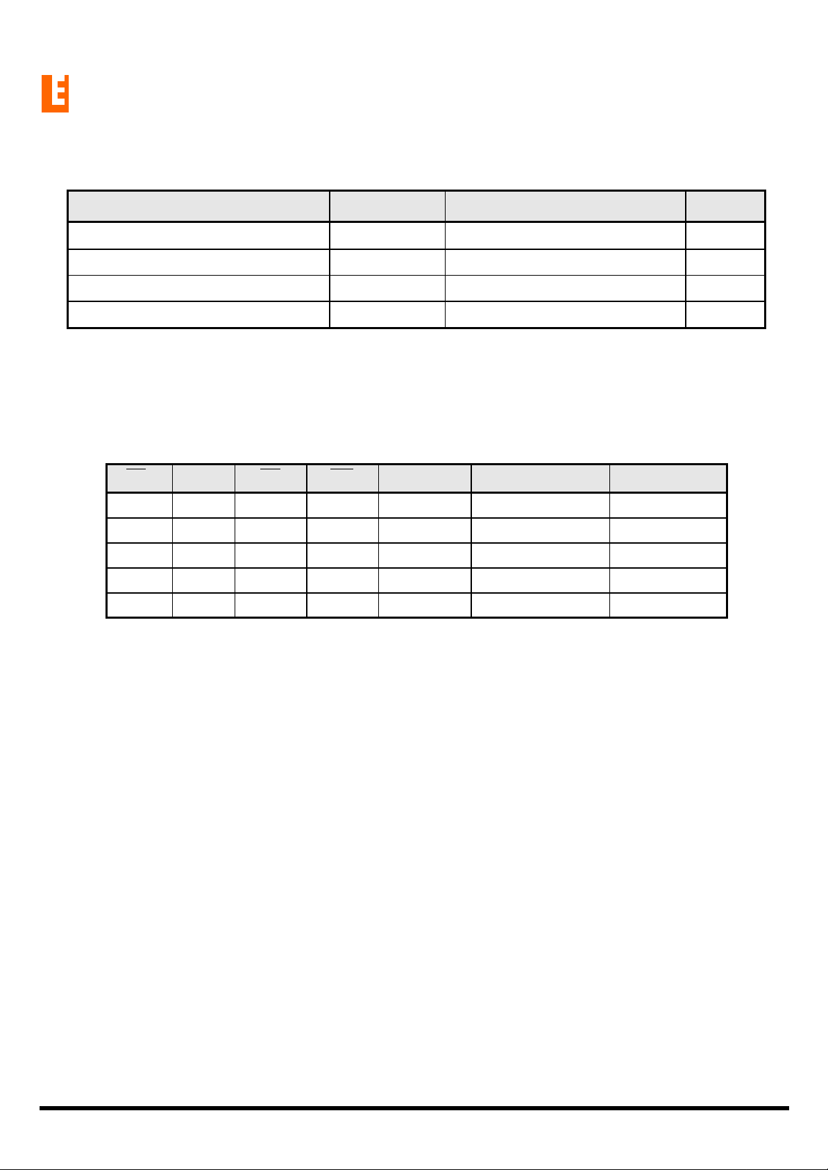
READ CYCLE (Vcc =2.7 to 3.6V, Gnd = 0V, TA = -40oC to +85oC)
1)
= 30pF + 1 TTL
EM620FV8AT Series
Low Power, 256Kx8 SRAM
3)
V
TM
2)
R
1
CL
1)
2)
R
2
Parameter
Read cycle time t
Address access time tAA - 55 - 70 ns
Chip select to output t
Output enable to valid output t
Chip select to low-Z output t
Output enable to low-Z output t
Chip disable to high-Z output t
Output disable to high-Z output t
Output hold from address change t
Symbol
RC
co1, tco2
OE
LZ1, tLZ2
OLZ
HZ1, tHZ2
OHZ
OH
55ns 70ns
Min Max Min Max
55 - 70 - ns
- 55 - 70 ns
- 25 - 35 ns
10 - 10 - ns
5 - 5 - ns
0 20 0 25 ns
0 20 0 25 ns
10 - 10 - ns
Unit
WRITE CYCLE
Parameter
Write cycle time t
Chip select to end of write t
Address setup time t
Address valid to end of write t
Write pulse width t
Write recovery time t
Write to ouput high-Z t
Data to write time overlap t
Data hold from write time t
End write to output low-Z t
(Vcc =2.7 to 3.6V, Gnd = 0V, TA = -40oC to +85oC)
55ns 70ns
Symbol
Min Max Min Max
WC
CW1, tCW2
As
AW
WP
WR
WHZ
DW
DH
OW
55 - 70 - ns
45 - 60 - ns
0 - 0 - ns
45 - 60 - ns
40 - 50 - ns
0 - 0 - ns
0 20 0 20 ns
25 30 ns
0 - 0 - ns
5 - 5 - ns
Unit
5
Rev 0.2

merging Memory & Logic Solutions Inc.merging Memory & Logic Solutions Inc.
TIMING DIAGRAMS
EM620FV8AT Series
Low Power, 256Kx8 SRAM
TIMING WAVEFORM OF READ CYCLE(1). (Address Controlled, CS1=OE=V
t
RC
Address
t
AA
t
OH
Data Out
TIMING WAVEFORM OF READ CYCLE(2) (WE = V
Address
CS1
Previous Data Valid
)
IH
t
RC
t
AA
t
CO
, CS2=WE=V
IL
Data Valid
t
OH
)
IH
CS2
t
HZ
t
OE
OE
t
OLZ
Data Out
NOTES (READ CYCLE)
1. tHZ and t
2. At any given temperature and voltage condition, tHZ(Max.) is less than tLZ(Min.) both for a given device and from device to device
interconnection.
are defined as the outputs achieve the open circuit conditions and are not referanced to output voltage levels.
OHZ
High-Z
Data Valid
t
LZ
t
OHZ
6
Rev 0.2
merging Memory & Logic Solutions Inc.merging Memory & Logic Solutions Inc.
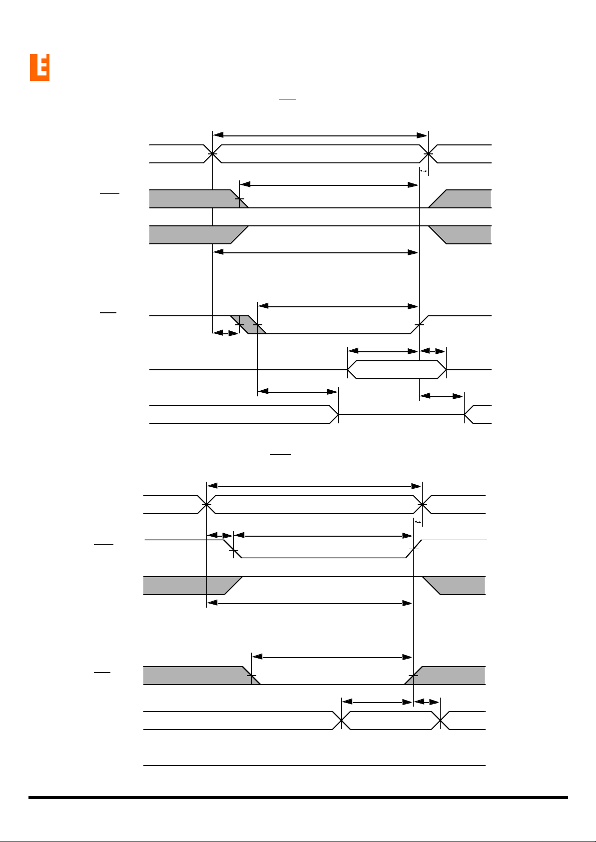
TIMING WAVEFORM OF WRITE CYCLE(1) (WE CONTROLLED)
t
WC
Address
EM620FV8AT Series
Low Power, 256Kx8 SRAM
tCW(2)
CS1
CS2
t
AW
tWP(1)
WE
tAS(3)
Data in
Data out
High-Z
Data Undefined
t
WHZ
TIMING WAVEFORM OF WRITE CYCLE(2) (CS1 CONTROLLED)
t
DW
Data Valid
tWR(4)
t
DH
t
OW
High-Z
Address
CS1
CS2
WE
Data in
Data out
t
WC
tAS(3)
tCW(2) tWR(4)
t
AW
tWP(1)
t
DW
Data Valid
High-Z High-Z
t
DH
7
Rev 0.2
merging Memory & Logic Solutions Inc.merging Memory & Logic Solutions Inc.
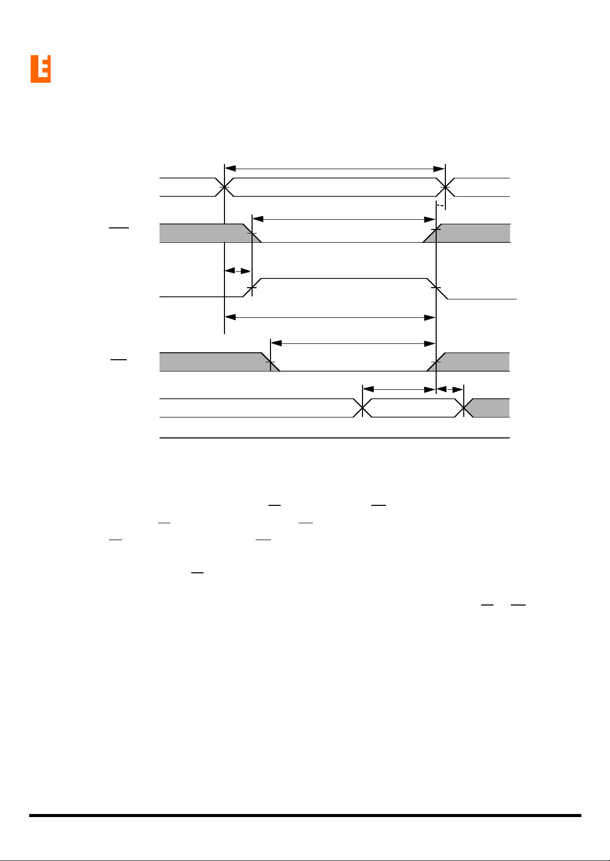
TIMING WAVEFORM OF WRITE CYCLE(3) ( CS2 CONTROLLED)
t
WC
Address
EM620FV8AT Series
Low Power, 256Kx8 SRAM
CS1
CS2
WE
Data in
Data out
NOTES (WRITE CYCLE)
tCW(2)
tAS(3)
t
AW
tWP(1)
t
DW
Data Valid
High-Z High-Z
tWR(4)
t
DH
1. A write occurs during the overlap(tWP) of low CS1, a high CS2 and low WE. A write begins at the latest
transition among CS1 goes low, CS2 goes high and WE goes low. A write ends at the earliest transition
when CS1 goes high, CS2 goes hagh and WE goes high. The tWP is measured from the beginning of write
to the end of write.
2. tCW is measured from the CS1 going low to end of write.
3. tAS is measured from the address valid to the beginning of write.
4. tWR is measured from the end or write to the address change. tWR applied in case a write ends as CS1 or WE
going high.
8
Rev 0.2

merging Memory & Logic Solutions Inc.merging Memory & Logic Solutions Inc.
DATA RETENTION CHARACTERISTICS
Parameter Symbol Test Condition Min Typ Max Unit
I
Test Condition
VCC for Data Retention V
DR
SB1
(Chip Disabled)
EM620FV8AT Series
Low Power, 256Kx8 SRAM
1)
1.5 - 3.6 V
Data Retention Current
Chip Deselect to Data Retention Time t
Operation Recovery Time t
NOTES
1. See the I
measurement condition of datasheet page 4.
SB1
DATA RETENTION WAVE FORM
CS1 Controlled
t
SDR
V
cc
2.7V
2.2V
I
SDR
RDR
DR
VCC=1.5V, I
(Chip Disabled)
See data retention wave form
Data Retention Mode
Test Condition
SB1
1)
- - 5 µA
0 - -
t
RC
t
RDR
- -
ns
V
DR
CS
1
GND
CS2 Controlled
V
cc
2.7V
CS
2
V
DR
0.4V
GND
t
SDR
CS1 > Vcc-0.2V
Data Retention Mode
CS2 < 0.2V
t
RDR
9
Rev 0.2
merging Memory & Logic Solutions Inc.merging Memory & Logic Solutions Inc.
EM620FV8AT Series
Low Power, 256Kx8 SRAM
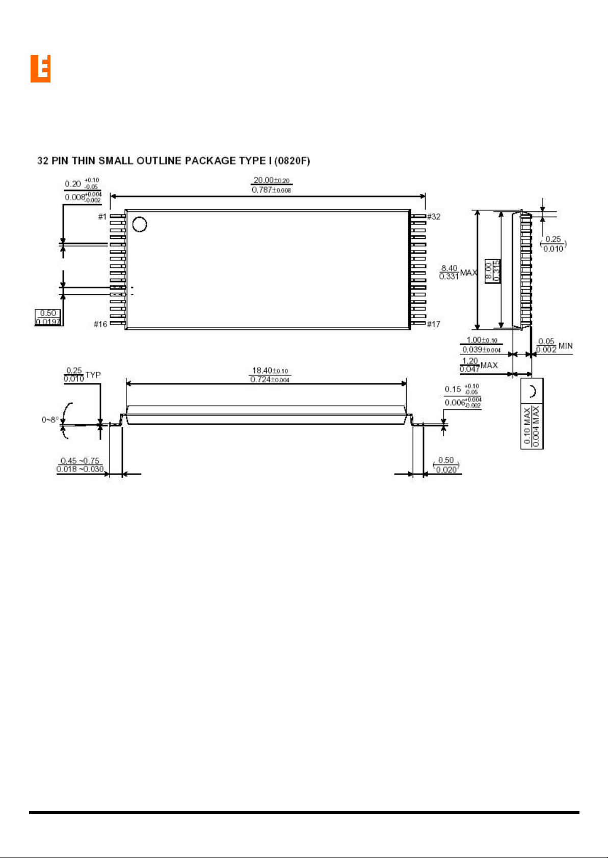
Unit : millimeters/Inches
10
Rev 0.2

merging Memory & Logic Solutions Inc.merging Memory & Logic Solutions Inc.
MEMORY FUNCTION GUIDE
EM X XX X X X XX X X - XX XX
EM620FV8AT Series
Low Power, 256Kx8 SRAM
1. EMLSI Memory
2. Device Type
3. Density
4. Option
5. Technology
6. Operating Voltage
1. Memory Component
2. Device Type
6 ------------------------ Low Power SRAM
7 ------------------------ STRAM
3. Density
1 ------------------------- 1M
2 ------------------------- 2M
4 ------------------------- 4M
8 ------------------------- 8M
16 ----------------------- 16M
32 ----------------------- 32M
64 ----------------------- 64M
4. Option
0 ----------------------- Dual CS
1 ----------------------- Single CS
5. Technology
Blank ------------------ CMOS
F ------------------------ Full CMOS
6. Operating Voltage
Blank ------------------ 5.0V
V ------------------------- 2.7V~3.6V
U ------------------------- 3.0V
S ------------------------- 2.5V
R ------------------------- 2.0V
P ------------------------- 1.8V
7. Orginzation
8 ---------------------- x8 bit
16 ---------------------- x16 bit
32 ---------------------- x32 bit
11. Power
10. Speed
9. Packages
8. Version
7. Orgainzation
8. Version
Blank ----------------- Mother Die
A ----------------------- First revision
B ----------------------- Second revision
C ----------------------- Third revision
D ----------------------- Fourth revision
E ----------------------- Fifth revision
F ----------------------- Sixth revision
9. Package
Blank ---------------------- FPBGA
S ---------------------------- 32 sTSOP1
T ---------------------------- 32 TSOP1
U ---------------------------- 44 TSOP2
W ---------------------------- Wafer
10. Speed
45 ---------------------- 45ns
55 ---------------------- 55ns
70 ---------------------- 70ns
85 ---------------------- 85ns
10 --------------------- 100ns
12 --------------------- 120ns
11. Power
LL ---------------------- Low Low Power
LF ---------------------- Low Low Power(Pb-Free)
L ---------------------- Low Power
S ---------------------- Standard Power
11
Rev 0.2
 Loading...