EMLSI EM620FV16B Service Manual

查询EM610FR16AS-45LF供应商
EM620FV16B Series
Low Power, 128Kx16 SRAM
Document Title
128K x16 bit Low Power and Low Voltage Full CMOS Static RAM
Revision History
Revision No. History Draft Date Remark
0.0 Initial Draft June 7, 2007
0.1 0.1 Revision Remove BYTE option information June 15, 2007
0.2 0.2 Revision Revised VOH(2.2v to 2.4v),tOH(15ns to 10ns),
tOE-55(30ns to 25ns), tWP-55(45ns to 40ns),
tWP-70(55ns to 50ns), tWHZ-70(25ns to 20ns),
ICC(2mA to 3mA), ICC1(2mA to 3mA)
0.3 0.3 Revision VIH level change from 2.0V to 2.2V Aug. 16, 2007
July 2, 2007
Emerging Memory & Logic Solutions Inc.
4F Korea Construction Financial Cooperative B/D, 301-1 Yeon-Dong, Jeju-Si, Jeju-Do, Rep.of Korea Zip Code : 690-719
Tel : +82-64-740-1712 Fax : +82-64-740-1749~1750 / Homepage : www.emlsi.com
The attached data sheets are provided by EMLSI reserve the right to change the specifications and products. EMLSI will answer to your
questions about device. If you have any questions, please contact the EMLSI office.
1

128K x16 Bit Low Power and Low Voltage CMOS Static RAM
FEATURES
- Process Technology : 0.15µm Full CMOS
- Organization :128K x16
- Power Supply Voltage
=> EM620FV16B : 2.7~3.6V
- Low Data Retention Voltage : 1.5V
- Three state output and TTL Compatible
- Packaged product designed for 45/55/70ns
56
EM620FV16B Series
Low Power, 128Kx16 SRAM
EM620FV16B (Dual C/S)
29
GENERAL PHYSICAL SPECIFICATIONS
- Backside die surface of polished bare silicon
- Typical Die Thickness = 725um +/-15um
- Typical top-level metallization :
=> Metal (Ti/AlCu/TiN/ARC SiON/SiO2) : 5.2K Angstroms
- Topside Passivation :
=> Passivation (HDP/pNIT/PIQ) : 5.4K Angstroms
- Wafer diameter : 8 inch
OPTIONS
- C1/W1 : DC Probed Die/Wafer @ Hot Temp
- C2/W2 : DC/AC Probed Die/Wafer @ Hot Temp
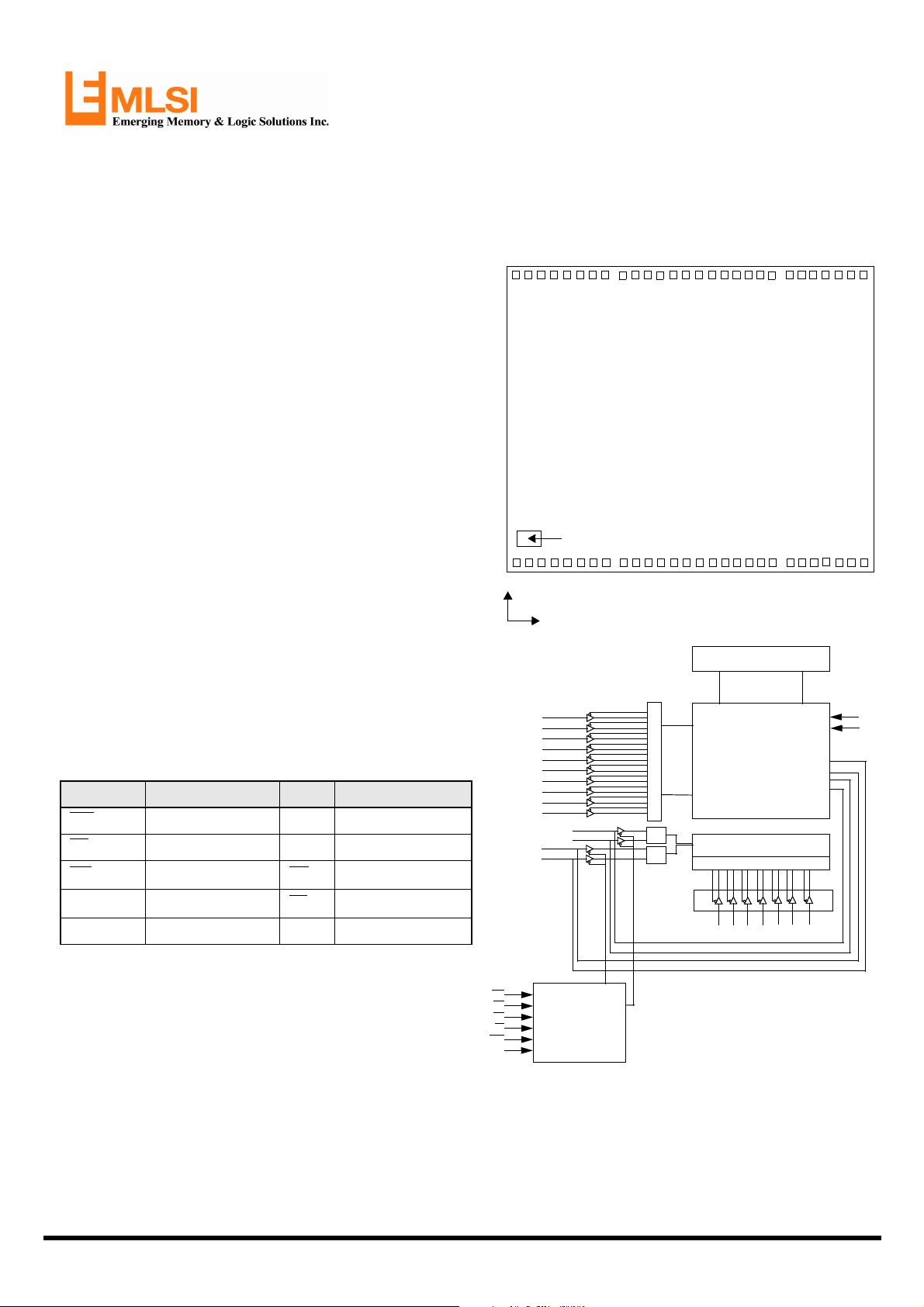
PAD DESCRIPTIONS
Name Function Name Function
CS1,CS2 Chip select inputs Vcc Power Supply
OE Output Enable input Vss Ground
WE Write Enable input UB
A0~A16 Address Inputs LB
I/O0~I/O15 Data Inputs/Outputs NC No Connection
Upper Byte (I/O
Lower Byte (I/O
8~15
0~7
)
)
y
x
I/O0 ~ I/O7
I/O8 ~ I/O15
A
0
A
1
A
2
A
3
A
4
A
5
A
6
A
7
A
8
A
9
EMLSI LOGO
+
Row Select
Data
Cont
Data
Cont
(0.0)
Pre-charge Circuit
Memory Array
1024 x 2048
I/O Circuit
Column Select
A
A
A
11
10
12
281
V
CC
V
SS
A
A
A
A
14
13
15
16
WE
OE
CS1
CS2
UB
LB
Control Logic
BONDING INSTRUCTIONS
The 2M full CMOS SRAM die has total 56pads. Refer to the bond pad location and identification table for X, Y coordinates.
EMLSI recommends using a bond wire on back side of die onto Vss bond pad for improved noise immunity.
2

EM620FV16B Series
Low Power, 128Kx16 SRAM
FUNCTIONAL SPECIFICATIONS
There are 3 classifications for EMLSI die and wafers products, which are C1 and C2 for die and W1 and W2 for wafer, respectively.
Each die and wafer support dedicated characteristics and probe the electrical parameters within their specifications. Followings are
brief information for die and wafer classifications. Please refer to packaged specifications for more information but these parameters
are not guaranteed at bare die and wafer.
− C1 LEVEL DIE OR W1 LEVEL WAFER
The DC parameters are measured by specification for C1 level die or W1 level wafer. The DC parameters measured at 70°C temperature, which called ‘Hot DC Sorting’ Other parameters are not guaranteed and warranted including device reliability. Please refer
to qualification report for device reliability and package level datasheets for electrical parameters.
− C2 LEVEL DIE OR W2 LEVEL WAFER
The DC parameters and selected AC parameters are measured with for C2 level die or W2 level wafer. The DC characteristics of C2
die and W2 wafer is tested based on DC specifications of C1 level die and W1 level wafer. The DC and specified AC parameters are
tested at 70°C temperature, which called ‘Hot DC & Selective AC Sorting’. Other parameters are not guaranteed and warranted
including device reliability. Please refer to qualification report for device reliability and package level datasheets for electrical parameters.
C2 level die and W2 level wafer probe following AC parameter.
− tRC, tAA, tCO
− tWC, tCW
PACKAGING
Individual device will be packed in anti-static trays.
− Chip Trays : A 2-inch square waffle style carrier for die with separate compartments for each die. Commonly referred to as a waffle
pack, each tray has a cavity size selected for the device that allows for easy loading and unloading and prevents
rotation. The tray itself is made of conductive material to reduce the danger of damage to the die from electrostatic
discharge. The chip carriers will be labeled with the following information :
− EMLSI wafer lot number
− EMLSI part number
− Quantity
− Jar Packing : Jar packing is made by EMLSI and used by many customers that we deliver the requested die as wafer. The pack is
consisted of clean paper to wrap the wafer, high cushioned sponge between wafers and hardly fragile plastic box with sponge. Each
pack has typically 24 wafers and then several packs are put into larger box depending on amounts of wafers.
Bond Pad #1 at Top
Die orientation in chip carriers
STORAGE AND HANDLING
EMLSI recommends the die stored in a controlled environment with filtered nitrogen. The carrier must be opened at ESD safe
environment when inspection and assembly.
3

ABSOLUTE MAXIMUM RATINGS *
Parameter Symbol Minimum Unit
EM620FV16B Series
Low Power, 128Kx16 SRAM
Voltage on Any Pin Relative to Vss VIN, V
Voltage on Vcc supply relative to Vss V
Power Dissipation P
Operating Temperature T
*
Stresses greater than those listed above “Absolute Maximum Ratings” may cause permanent damage to the device. Functional operation should be restricted to recommended operating condition. Exposure to absolute maximum rating conditions for extended periods
may affect reliability.
OUT
CC
D
A
-0.2 to 4.0V V
-0.2 to 4.0V V
1.0 W
-40 to 85
o
C
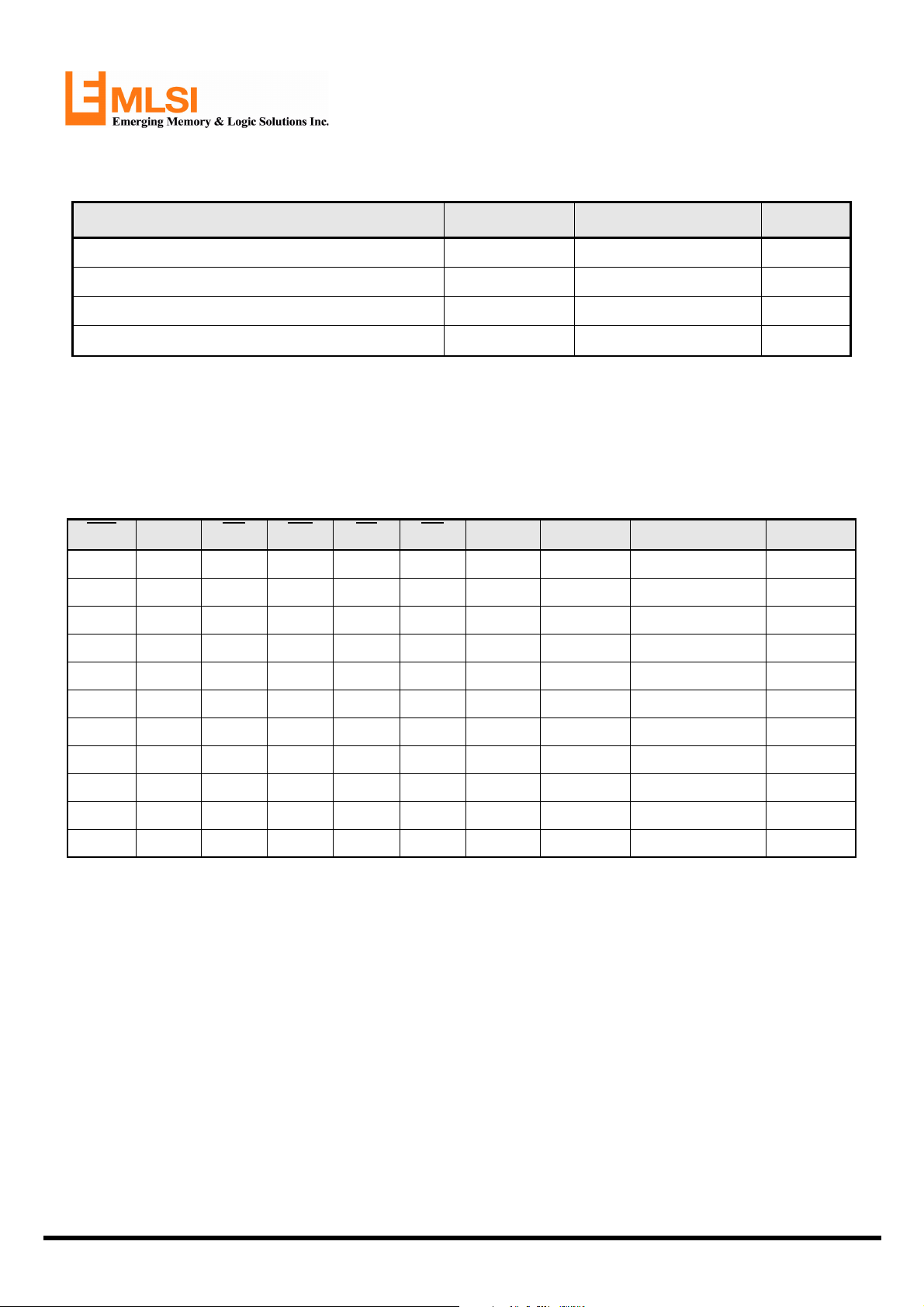
FUNCTIONAL DESCRIPTION
CS1 CS2 OE WE LB UB I/O
0-7
H X X X X X High-Z High-Z Deselected Stand by
X L X X X X High-Z High-Z Deselected Stand by
X X X X H H High-Z High-Z Deselected Stand by
L H H H L X High-Z High-Z Output Disabled Active
L H H H X L High-Z High-Z Output Disabled Active
I/O
8-15
Mode Power
L H L H L H Data Out High-Z Lower Byte Read Active
L H L H H L High-Z Data Out Upper Byte Read Active
L H L H L L Data Out Data Out Word Read Active
L H X L L H Data In High-Z Lower Byte Write Active
L H X L H L High-Z Data In Upper Byte Write Active
L H X L L L Data In Data In Word Write Active
Note: X means don’t care. (Must be low or high state)
4
 Loading...