

User Guide
SI-I/O
Part Number: 0478-0047-03
Issue: 3
www.controltechniques.com

General Information
The manufacturer accepts no liability for any consequences resulting from inappropriate, negligent or incorrect installation or adjustment of the optional
operating parameters of the equipment or from mismatching the variable speed drive with the motor.
The contents of this guide are believed to be correct at the time of printing. In the interests of a commitment to a policy of continuous development and
improvement, the manufacturer reserves the right to change the specification of the product or its performance, or the contents of this guide, without
notice.
All rights reserved. No parts of this guide may be reproduced or transmitted in any form or by any means, electrical or mechanical including
photocopying, recording or by an information storage or retrieval system, without permission in writing from the publisher.
Drive software version
The SI-I/O can only be used with drive software version 01.02.00.xx onwards.

Contents
1 How to use this guide ...........................4
1.1 Intended personnel ...............................................4
1.2 Information ............................................................4
2 Safety information .................................5
2.1 Warnings, Cautions and Notes .............................5
2.2 Electrical safety - general warning ........................5
2.3 System design and safety of personnel ................5
2.4 Environmental limits ..............................................5
2.5 Access ..................................................................5
2.6 Compliance with regulations .................................5
2.7 Adjusting parameters ............................................5
2.8 Stored charge .......................................................6
3 Introduction ...........................................7
3.1 Features ................................................................7
3.2 Option module identification ..................................7
3.3 Conventions used in this guide .............................7
3.4 Digital I/O ..............................................................8
3.5 Analog I/O .............................................................8
3.6 Relays ...................................................................8
3.7 24 V internal power supply ....................................8
4 Mechanical installation .........................9
4.1 General installation ...............................................9
10 Technical Data .....................................36
10.1 Digital inputs/outputs (Terminals 2-5) .................36
10.2 Digital Inputs (Terminals 7-9) ..............................36
10.3 Differential Analog Input (Terminals 7 and 8) ......36
10.4 Single-ended Analog Inputs (Terminals 7-9)
in Voltage input mode .........................................37
10.5 Single-ended Analog Input (Terminal 9) in
Current input mode .............................................37
10.6 Analog Output (Terminal 11) in Voltage
output mode ........................................................37
10.7 Analog Output (Terminal 11) in Current
output mode ........................................................38
10.8 Relays (Terminals 21-23) ....................................38
5 Electrical installation ..........................10
5.1 Terminal descriptions ..........................................10
5.2 Wiring, shield connections ..................................10
6 Single line descriptions ...................... 11
6.1 Single line descriptions .......................................11
6.2 Menu 9 - Resources ............................................14
7 Parameters ...........................................15
7.1 Menu 0 - Module Set-up .....................................15
7.2 Menu 1 - I/O Set-up ............................................18
7.3 Menu 2 - Digital I/O .............................................23
7.4 Menu 3 - Analog I/O ............................................24
7.5 Menu 9 - Resources ............................................27
8 Block diagrams ...................................28
8.1 Functional block diagrams ..................................28
9 Diagnostics ..........................................34
9.1 Overview .............................................................34
SI-I/O User Guide 3
Issue Number: 3

How to use
this guide
Safety
information
Introduction
Mechanical
installation
Electrical
installation
Single line
descriptions
Parameters Block diagrams Diagnostics Technical Data Index
1 How to use this guide
1.1 Intended personnel
This guide is intended for personnel who have the necessary training and experience in system design, installation, commissioning and maintenance.
1.2 Information
This guide contains information covering the identification of the option module, terminal layout for installation, fitting of the option module to the drive,
parameter details, diagnostic information and the specifications of the option module.
4 SI-I/O User Guide
Issue Number: 3

How to use this
WARNING
CAUTION
NOTE
guide
Safety
information
Introduction
Mechanical
installation
Electrical
installation
Single line
descriptions
Parameters Block diagrams Diagnostics Technical Data Index
2 Safety information
2.1 Warnings, Cautions and Notes
A Warning contains information which is essential for avoiding a safety hazard.
A Caution contains information which is necessary for avoiding a risk of damage to the product or other equipment.
A Note contains information which helps to ensure correct operation of the product.
2.2 Electrical safety - general warning
The voltages used in the drive can cause severe electrical shock and/or burns, and could be lethal. Extreme care is necessary at all times when
working with or adjacent to the drive.
Specific warnings are given at the relevant places in this User Guide.
2.3 System design and safety of personnel
The drive is intended as a component for professional incorporation into complete equipment or a system. If installed incorrectly, the drive may
present a safety hazard.
The drive uses high voltages and currents, carries a high level of stored electrical energy, and is used to control equipment which can cause injury.
Close attention is required to the electrical installation and the system design to avoid hazards either in normal operation or in the event of equipment
malfunction. System design, installation, commissioning/start-up and maintenance must be carried out by personnel who have the necessary training
and experience. They must read this safety information and this User Guide carefully.
The STOP and SAFE TORQUE OFF functions of the drive do not isolate dangerous voltages from the output of the drive or from any external option
unit. The supply must be disconnected by an approved electrical isolation device before gaining to the electrical connections.
With the sole exception of the SAFE TORQUE OFF function, none of the drive functions must be used to ensure safety of personnel, i.e.
they must not be used for safety-related functions.
Careful consideration must be given to the functions of the drive which might result in a hazard, either through their intended behavior or through
incorrect operation due to a fault. In any application where a malfunction of the drive or its control system could lead to or allow damage, loss or injury,
a risk analysis must be carried out, and where necessary, further measures taken to reduce the risk - for example, an over-speed protection device in
case of failure of the speed control, or a fail-safe mechanical brake in case of loss of motor braking.
The system designer is responsible for ensuring that the complete system is safe and designed correctly according to the relevant safety
standards.
2.4 Environmental limits
Instructions regarding transport, storage, installation and use of the drive must be complied with, including the specified environmental limits. These
instructions can be found in the relevant drive documentation. Drives must not be subjected to excessive physical force.
2.5 Access
Drive access must be restricted to authorized personnel only. Safety regulations which apply at the place of use must be complied with.
2.6 Compliance with regulations
The installer is responsible for complying with all relevant regulations, such as national wiring regulations, accident prevention regulations and
electromagnetic compatibility (EMC) regulations. Particular attention must be given to the cross-sectional areas of conductors, the selection of fuses
or other protection, and protective ground (earth) connections.
Instructions for achieving compliance with specific EMC standards may be found in the relevant drive documentation.
Within the European Union, all machinery in which this product is used must comply with the following directives:
2006/42/EC: Safety of machinery.
2004/108/EC: Electromagnetic Compatibility.
2.7 Adjusting parameters
Some parameters have a profound effect on the operation of the drive. They must not be altered without careful consideration of the impact on the
controlled system. Measures must be taken to prevent unwanted changes due to error or tampering.
SI-I/O User Guide 5
Issue Number: 3

How to use this
guide
Safety
information
Introduction
Mechanical
installation
Electrical
installation
Single line
descriptions
Parameters Block diagrams Diagnostics Technical Data Index
2.8 Stored charge
The drive contains capacitors which remain charged to a potentially lethal voltage after the AC supply has been disconnected. If the drive has been
energized, the AC supply must be isolated for at least ten minutes before work may continue.
6 SI-I/O User Guide
Issue Number: 3

How to use this
1
2
SI-I/O
guide
Safety
information
Introduction
Mechanical
installation
Electrical
installation
Single line
descriptions
Parameters Block diagrams Diagnostics Technical Data Index
3 Introduction
3.1 Features
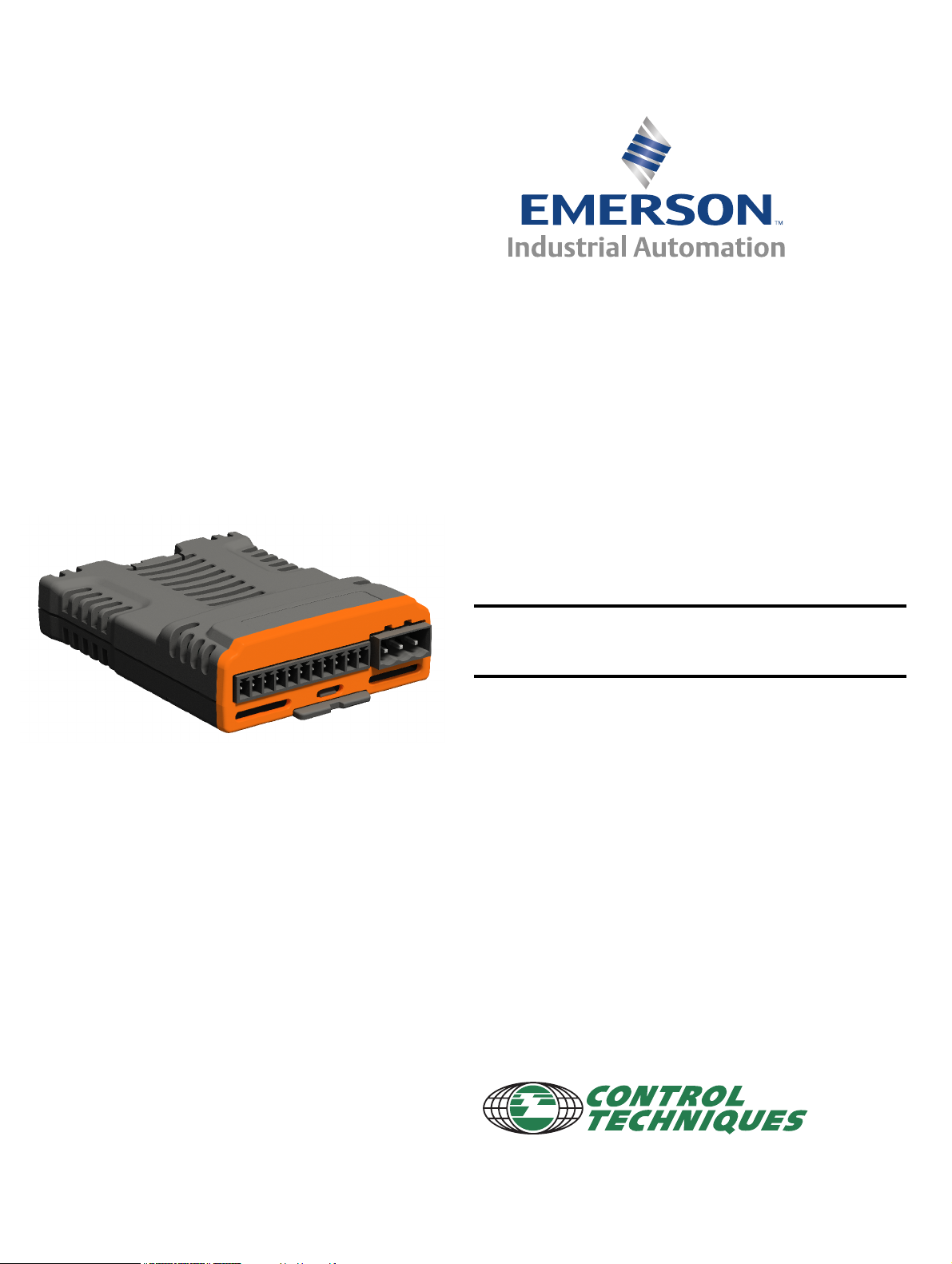
All connections from the Option module to the drive are made via the drive connector. Connections from external equipment to the SI-I/O are made
via a 3-way plugable/removable screw connector for the two relays, and an 11-way plugable/removable screw connector for the digital and analog
I/O.
Figure 3-1 SI-I/O
All parameters associated with the SI-I/O can be found in section 7 Parameters on page 15.
3.2 Option module identification
SI-I/O can be identified by:
1. The label located on the top of the Option module.
2. The color coding across the front of the SI-I/O (Orange).
Figure 3-2 SI-I/O labels
1 Topside module label
2 Underside module label
3.2.1 Date code format
The date code is split into two sections: a letter followed by a number. The letter indicates the year, and the number indicates the week number (within
the year) in which the Option module was built.The letters go in alphabetical order, starting with A in 1990 (B in 1991, C in 1992 etc).
Example:
A date code of V35 would correspond to week 35 of year 2012.
3.3 Conventions used in this guide
The configuration of the host drive and Option module is done using menus and parameters. A menu is a logical collection of parameters that have
similar functionality. In the case of an Options module, the parameters will appear in menu 15, 16 or 17 depending on which slot the module is
installed to. The menu is determined by the number before the decimal point.
The method used to determine the menu or parameter is as follows:
•Pr S.mm.ppp - Where S signifies the Option module slot number and mm.ppp signifies the menu and parameter number of the Option module's
internal menus and parameters.
•Pr MM.ppp - Where MM signifies the menu allocated to the Option module set-up menu and ppp signifies the parameter number.
Pr mm.000 - Signifies parameter number 000 in any drive menu.
All the inputs/outputs in the SI-I/O are user programmable for function and signal processing.
SI-I/O User Guide 7
Issue Number: 3

How to use this
NOTE
NOTE
NOTE
NOTE
guide
Safety
information
Introduction
Mechanical
installation
Electrical
installation
Single line
descriptions
Parameters Block diagrams Diagnostics Technical Data Index
3.4 Digital I/O
By default, the digital inputs/outputs on the Option module are configured to operate in positive logic.
Configuration of the maximum of eight digital inputs for positive/negative logic is carried out by setting Pr S.01.008.
By default, the SI-I/O Module is set up for four programmable digital inputs/outputs. By configuring the analog I/O as digital inputs, it is possible for the
SI-I/O module to have four programmable inputs/outputs and also four digital inputs.
The functionality of these terminals is as follows:
• The logic sense selected can be positive or negative
• The logic state of each input is monitored by a read-only parameter
• The logic state can be inverted
• The digital input can be programmed to any suitable destination bit parameter
• The digital output can be sourced from any suitable bit parameter
• The output can operate either as a push-pull or an open collector output
3.5 Analog I/O
By default, the SI-I/O is set up for three single-ended analog inputs and one analog output or one high resolution differential analog input, one singleended analog input and one analog output.
Analog inputs 1 and 2 can only be configured as ±10 Vdc voltage inputs or digital inputs. When both are configured as analog voltage inputs, they can
be used as a single high resolution differential analog input.
Analog input 3 can operate in voltage mode (±10 Vdc), current mode (0 to 20 mA) or as a digital input.
Analog output 1 can operate in voltage mode (±10 Vdc), current mode (0 to 20 mA) or as a digital input.
The high precision differential analog input and analog output is only supported on Unidrive M600 - M800.
3.6 Relays
The two relays can be used to convey the logic state of any suitable parameter to external equipment. The logic state is processed as follows:
• A suitable source parameter is assigned to each relay
• The logic state can be inverted
• The state of the relay is monitored by a parameter
3.7 24 V internal power supply
If the user load exceeds 400 mA at 24 V, (24 V internal power supply), then an external
24 V power supply will be required which should be connected to the drive’s control terminals 1 and 2.
The user load comprises of:
• The drive’s digital outputs plus the SI-I/O digital outputs
Or
• The drive’s main encoder supply
The maximum output current from the drive’s digital output terminals 22, 24, 25 and 26 is 240 mA at 24 V, exceeding this will result in an ‘Output
overload’ digital output overload trip.
The SI-I/O has a maximum output current of 250 mA at 24 V across all four digital outputs.
If the maximum current of the drive and Option modules is exceeded a ‘PSU 24V' 24 V internal power supply overload trip will result.
8 SI-I/O User Guide
Issue Number: 3

How to use this
1
2
3
guide
Safety
information
Introduction
Mechanical
installation
Electrical
installation
Single line
descriptions
Parameters Block diagrams Diagnostics Technical Data Index
4 Mechanical installation
4.1 General installation
The installation of an Option module is illustrated in Figure 4-1.
Figure 4-1 Installing an Option module
1 2
4.1.1 Installing the first Option module
• Option module slots must be used in the following order: slot 3, slot 2 and slot 1. Orientate the Option module above the drive as shown in (1).
Align and insert the Option module tab into the slot (2). Press down on the Option module until it clicks into place.
Adding Option modules: Populate slot 3 first, then slot 2 and finally slot 1
SI-I/O User Guide 9
Issue Number: 3

How to use this
123456789
PL1
10 11 21 22 23
PL2
+
0V
+
0V
+
0V
+
0V
+
Analog Input 1
Analog Input 2
Analog Input 3
Analog Output 1
0V Common
0V Common
0V Common
0V Common
-
0V
0V Common
Differential Anal
ogInput
+
Differential Anal
ogInput
-
guide
Safety
information
Introduction
Mechanical
installation
Electrical
installation
Single line
descriptions
Parameters Block diagrams Diagnostics Technical Data Index
5 Electrical installation
5.1 Terminal descriptions
Table 5.1 SI-IO terminal descriptions
Table 5.2 11 way user connector and relay pin numbering
PL1 Function PL2 Function
T1 0 V common T21 Relay 1
T2 Digital input/output 1 T22 Relay common
T3 Digital input/output 2 T23 Relay 2
T4 Digital input/output 3 3 way 5.08 mm plugable screw connector
T5 Digital input/output 4
T6 0 V common
T7 Analog input 1/digital input 5
T8 Analog input 2/digital input 6
T9 Analog input 3/digital input 7
T10 0 V common
T11 Analog output 1/digital input 8
11 way 3.81 mm plugable screw connector
5.2 Wiring, shield connections
To prevent noise being induced onto any of the analog inputs or outputs, it is advisable to use twisted pair cable shielded with an overall outer shield.
The shield connections should be terminated at one of the zero volt terminals on the Option module, and to the zero volt connection of the signal
source. The termination of the shield should be kept as short as possible to prevent and noise being induced in this area.
Figure 5-1 Shield connections
10 SI-I/O User Guide
Issue Number: 3

How to use this
guide
Safety
information
Introduction
Mechanical
installation
Electrical
installation
Single line
descriptions
Parameters Block diagrams Diagnostics Technical Data Index
6 Single line descriptions
6.1 Single line descriptions
6.1.1 Menu 0 - Setup
Parameter Range (Ú) Default (Ö)Type
MM.001 Module ID 0 to 999
MM.002 Software Version 00.00.00.00 to 99.99.99.99
MM.003 Hardware Version 00.00 to 99.99
MM.004 Serial Number LS 0 to 99999999
MM.005 Serial Number MS 0 to 99999999
MM.006 Module status Initializing (0), OK (1), Config (2), Error (3)
MM.007 Module reset Off (0) or On (1)
MM.008 Module default Off (0) or On (1)
MM.030 Slot Indicator 0 to 8
MM.031 Slot Menu Number 0 to 255
6.1.2 Menu 1 - I/O Setup
Parameter Range (Ú) Default (Ö)Type
S.01.001 Reset I/O Interface Off (0) or On (1) Off (0) RW Bit NC
S.01.002 Default I/O Interface Off (0) or On (1) Off (0) RW Bit NC
S.01.004 Option Module Status Initializing (0), OK (1), Config (2), Error (3)
S.01.005
I/O Output Enable
Register
S.01.006 I/O Input Register 00000000 to 11111111
S.01.007 I/O Output Register 0000000000 to 1111111111 0000000000 RW Bin US
S.01.008 Digital I/O Logic Polarity Negative Logic (0) or Positive Logic (1) Positive Logic (1) RW Txt US
S.01.009 Open Collector Output Push-Pull (0) or Open Collector (1) Push-Pull (0) RW Txt US
S.01.010 I/O Read Word 0000000000 to 1111111111 0000000000 RO Bin
S.01.011 T2 Digital I/O 1 Mode Digital Input (0) or Digital Output (1) Digital Input (0) RW Txt US
S.01.012 T3 Digital I/O 2 Mode Digital Input (0) or Digital Output (1) Digital Input (0) RW Txt US
S.01.013 T4 Digital I/O 3 Mode Digital Input (0) or Digital Output (1) Digital Input (0) RW Txt US
S.01.014 T5 Digital I/O 4 Mode Digital Input (0) or Digital Output (1) Digital Input (0) RW Txt US
S.01.015
S.01.016
T7 Digital Input 5 /
Analog Input 1 Mode
T8 Digital Input 6 /
Analog Input 2 Mode
Digital Input (0), Volt IN (1), 4-20mA Low (2), 20-
S.01.017
S.01.018
T9 Digital Input 7 /
Analog Input 3 Mode
T11 Digital Input 8 /
Analog Output 1 Mode
4mA Low (3), 4-20mA Hold (4), 20-4mA Hold (5),
0-20mA (6), 20-0mA (7), 4-20mA Trip (8), 20-
Digital Input (0), Volt Out (1), 4-20mA (2), 20-
0000000000 to 1111111111 0000000000 RW Bin US
Digital Input (0) or Volt IN (1) Volt IN (1) RW Txt US
Digital Input (0) or Volt IN (1) Volt IN (1) RW Txt US
4mA Trip (9), 4-20mA (10), 4-20mA (11)
4mA (3), 0-20mA (4), 20-0mA (5),
209
RO Num ND NC PT
RO Num ND NC PT
RO Num ND NC PT
RO Num ND NC PT
RO Num ND NC PT
RO Num ND NC PT
Off (0)
Off (0)
RW Bit NC
RW Bit NC
RO Num ND NC PT
RO Num ND NC PT
RO Txt ND NC PT
RO Bin US
Volt IN (1) RW Txt US
Volt Out (1) RW Txt US
SI-I/O User Guide 11
Issue Number: 3
How to use this
guide
Safety
information
Introduction
Mechanical
installation
Electrical
installation
Single line
descriptions
Parameters Block diagrams Diagnostics Technical Data Index
6.1.3 Menu 2 - Digital I/O
Parameter Range (Ú) Default (Ö)Type
S.02.001 Digital I/O 1 State Off (0) or On (1)
S.02.002 Digital I/O 2 State Off (0) or On (1)
S.02.003 Digital I/O 3 State Off (0) or On (1)
S.02.004 Digital I/O 4 State Off (0) or On (1)
S.02.005 Digital Input 5 State Off (0) or On (1)
S.02.006 Digital Input 6 State Off (0) or On (1)
S.02.007 Digital Input 7 State Off (0) or On (1)
S.02.008 Digital Input 8 State Off (0) or On (1)
S.02.009 Relay 1 State Off (0) or On (1)
S.02.010 Relay 2 State Off (0) or On (1)
S.02.011 Digital I/O 1 Invert Off (0) or On (1) Off (0) RW Bit US
S.02.012 Digital I/O 2 Invert Off (0) or On (1) Off (0) RW Bit US
S.02.013 Digital I/O 3 Invert Off (0) or On (1) Off (0) RW Bit US
S.02.014 Digital I/O 4 Invert Off (0) or On (1) Off (0) RW Bit US
S.02.015 Digital Input 5 Invert Off (0) or On (1) Off (0) RW Bit US
S.02.016 Digital Input 6 Invert Off (0) or On (1) Off (0) RW Bit US
S.02.017 Digital Input 7 Invert Off (0) or On (1) Off (0) RW Bit US
S.02.018 Digital Input 8 Invert Off (0) or On (1) Off (0) RW Bit US
S.02.019 Relay 1 Invert Off (0) or On (1) Off (0) RW Bit US
S.02.020 Relay 2 Invert Off (0) or On (1) Off (0) RW Bit US
S.02.021 Digital I/O 1 Source / Destination 0.00.000 to 4.99.999 0.00.000 RW Num PT US
S.02.022 Digital I/O 2 Source / Destination 0.00.000 to 4.99.999 0.00.000 RW Num PT US
S.02.023 Digital I/O 3 Source / Destination 0.00.000 to 4.99.999 0.00.000 RW Num PT US
S.02.024 Digital I/O 4 Source / Destination 0.00.000 to 4.99.999 0.00.000 RW Num PT US
S.02.025 Digital Input 5 Destination 0.00.000 to 4.99.999 0.00.000 RW Num PT US
S.02.026 Digital Input 6 Destination 0.00.000 to 4.99.999 0.00.000 RW Num PT US
S.02.027 Digital Input 7 Destination 0.00.000 to 4.99.999 0.00.000 RW Num PT US
S.02.028 Digital Input 8 Destination 0.00.000 to 4.99.999 0.00.000 RW Num PT US
S.02.029 Relay 1 Source 0.00.000 to 4.99.999 0.00.000 RW Num PT US
S.02.030 Relay 2 Source 0.00.000 to 4.99.999 0.00.000 RW Num PT US
RO Bit ND NC PT
RO Bit ND NC PT
RO Bit ND NC PT
RO Bit ND NC PT
RO Bit ND NC PT
RO Bit ND NC PT
RO Bit ND NC PT
RO Bit ND NC PT
RO Bit ND NC PT
RO Bit ND NC PT
12 SI-I/O User Guide
Issue Number: 3

How to use this
guide
Safety
information
Introduction
Mechanical
installation
Electrical
installation
Single line
descriptions
Parameters Block diagrams Diagnostics Technical Data Index
6.1.4 Menu 3 - Analog I/O
Parameter Range (Ú) Default (Ö)Type
S.03.001 Analog Input 1 -100.00 to 100.00%
S.03.002 Analog Input 2 -100.00 to 100.00%
S.03.003 Analog Input 3 -100.00 to 100.00%
S.03.004 Differential Analog Input -100.0000 to 100.0000%
S.03.005 Analog Output 1 -100.00 to 100.00%
S.03.006 Analog Output 1 Source 0.00.000 to 4.99.999 0.00.000 RW Num US
S.03.007 Analog Output 1 Scaling 0.000 to 40.000 1.000 RW Num US
S.03.011 Analog Input 1 Offset -100.00 to 100.00% 0.00% RW Num US
S.03.012 Analog Input 1 Scaling 0.000 to 40.000 1.000 RW Num US
S.03.013 Analog Input 1 Invert Off (0) or On (1) Off (0) RW Bit US
S.03.014 Analog Input 1 Minimum -100.00 to 100.00% -100.00% RW Num US
S.03.015 Analog Input 1 Maximum -100.00 to 100.00% 100.00% RW Num US
S.03.016 Analog Input 1 Destination 0.00.000 to 4.99.999 0.00.000 RW Num DE US
S.03.021 Analog Input 2 Offset -100.00 to 100.00% 0.00% RW Num US
S.03.022 Analog Input 2 Scaling 0.000 to 40.000 1.000 RW Num US
S.03.023 Analog Input 2 Invert Off (0) or On (1) Off (0) RW Bit US
S.03.024 Analog Input 2 Minimum -100.00 to 100.00% -100.00% RW Num US
S.03.025 Analog Input 2 Maximum -100.00 to 100.00% 100.00% RW Num US
S.03.026 Analog Input 2 Destination 0.00.000 to 4.99.999 0.00.000 RW Num DE US
S.03.031 Analog Input 3 Offset -100.00 to 100.00% 0.00% RW Num US
S.03.032 Analog Input 3 Scaling 0.000 to 40.000 1.000 RW Num US
S.03.033 Analog Input 3 Invert Off (0) or On (1) Off (0) RW Bit US
S.03.034 Analog Input 3 Minimum -100.00 to 100.00% -100.00% RW Num US
S.03.035 Analog Input 3 Maximum -100.00 to 100.00% 100.00% RW Num US
S.03.036 Analog Input 3 Destination 0.00.000 to 4.99.999 0.00.000 RW Num DE US
S.03.037 Analog Input 3 Current Loop Loss Off (0) or On (1)
S.03.041 Differential Analog Input Offset -100.00 to 100.00% 0.00% RW Num US
S.03.042 Differential Analog Input Scaling 0.000 to 40.000 1.000 RW Num US
S.03.043 Differential Analog Input Invert Off (0) or On (1) Off (0) RW Bit US
S.03.044 Differential Analog Input Minimum -100.00 to 100.00% -100.00% RW Num US
S.03.045 Differential Analog Input Maximum -100.00 to 100.00% 100.00% RW Num US
S.03.046 Differential Analog Input Destination 0.00.000 to 4.99.999 0.00.000 RW Num DE US
RO Num ND NC PT
RO Num ND NC PT
RO Num ND NC PT
RO Num ND NC PT
RO Num ND NC PT
RO Num ND NC PT
SI-I/O User Guide 13
Issue Number: 3

How to use this
guide
Safety
information
Introduction
Mechanical
installation
Electrical
installation
Single line
descriptions
6.2 Menu 9 - Resources
Parameter Range (Ú) Default (Ö)Type
S.09.030 PCB temperature -128 to 127°C
S.09.031 CPU Core Temperature -128 to 127°C
Parameters Block diagrams Diagnostics Technical Data Index
RO Num ND NC PT
RO Num ND NC PT
14 SI-I/O User Guide
Issue Number: 3

How to use this
guide
Safety
information
Introduction
Mechanical
installation
Electrical
installation
Single line
descriptions
Parameters Block diagrams Diagnostics Technical Data Index
7 Parameters
7.1 Menu 0 - Module Set-up
All parameters in S.00.ppp (i.e. menu 0 within the option module menus) are also present in menus 15, 16 or 17 depending on the slot that the
module is installed to e.g. Pr 3.00.007 is also present as 17.007.
The functionality and properties of the parameters are identical between the two menus.
S.00.001 Module ID
Minimum 0 Maximum 65535
Default 209 Units
Type 16 Bit Volatile Update Rate Power-up write
Display Format None Decimal Places 0
Coding RO, ND, NC, PT, BU
Pr S.00.001 displays the ID number for the Option Module. For SI-I/O, this is 209.
S.00.002 Firmware version
Minimum
0 (Display
00.00.00.00)
Maximum
Default Units
Type 32 Bit Volatile Update Rate Power-up write
Display Format Version Number Decimal Places 0
Coding RO, ND, NC, PT
The firmware version of the option module is in the format of ww.xx.yy.zz
99999999 (Display
99.99.99.99)
S.00.003 Hardware version
Minimum 00.00 Maximum 99.99
Default Units
Type 16 Bit Volatile Update Rate Power-up write
Display Format None Decimal Places 2
Coding RO, ND, NC, PT
The firmware version of the option module is in the format of ww.xx.yy.zz
S.00.004 Serial Number LS
S.00.005 Serial Number MS
Minimum 0 Maximum 99999999
Default Units
Type 32 Bit Volatile Update Rate Power-up write
Display Format None Decimal Places 0
Coding RO, ND, NC, PT
The module serial number is available as a pair of 32-bit values where Serial Number LS (Pr S.00.004) provide the least significant 8 decimal digits,
and Serial Number MS (Pr S.00.005) provides the most significant 8 decimal digits. The reconstructed serial number is ((S.00.005 x 100000000) +
S.00.004). For example serial number "0001234567898765" would be stored as S.00.005 = 123456 and S.00.004 = 67898765.
SI-I/O User Guide 15
Issue Number: 3

How to use this
NOTE
guide
Safety
information
Introduction
Mechanical
installation
Electrical
installation
Single line
descriptions
Parameters Block diagrams Diagnostics Technical Data Index
S.00.006 Module Status
Minimum 0 Maximum 101
Default Units
Type 8 Bit Volatile Update Rate Background read
Display Format None Decimal Places 0
Coding RO, TE, ND, NC, PT
This parameter displays the current status of the module. All possible values are shown in the table below.
Value Text Description
0 Initializing Module is currently initializing.
1 Ok Module has initialized and has found no errors.
2 Config
3Error
A configuration error has been detected in one of the
communications protocols or user program
An error has occurred preventing the firmware or user program
from running correctly.
100 Bootloader The bootloader is currently running.
101 Updating
The bootloader is currently performing a firmware update. The
power must not be turned off in this state.
S.00.007 Reset Module
Minimum 0 Maximum 1
Default 0 Units
Type 1 Bit Volatile Update Rate Read every 200 ms
Display Format None Decimal Places 0
Coding RW, NC
Changes to the module's configuration will not take effect until the module has been reset.
• To reset the module:
•Set Pr S.00.007 to On (1).
• When the sequence has been completed, Pr S.00.007 will be reset to Off (0).
The module will reset using the updated configuration.
This sequence does NOT store the module's configuration parameters in the drive or the module's flash memory. This parameter will change back to
Off immediately, and as such the change may not be visible in the display.
S.00.008 Default Module
Minimum 0 Maximum 1
Default 0 Units
Type 1 Bit Volatile Update Rate Read every 200 ms
Display Format None Decimal Places 0
Coding RW, NC
If the host drive is defaulted (see the drive user guide for details), it will also clear the current configuration for the slot the module is installed to.
This can be performed as follows:
•Set Pr S.00.008 to On.
• Reset the module by setting Pr S.00.007 to On.
• Default parameter values for the module will be loaded.
The module will reset using the default values.
S.00.030 Slot Indicator
Minimum 0 Maximum 8
Default Units
Type 8 Bit Volatile Update Rate Written on power-up
Display Format None Decimal Places 0
Coding RO, ND, NC, PT, BU
This parameter shows the slot number that the module is installed in.
16 SI-I/O User Guide
Issue Number: 3

How to use this
guide
Safety
information
Introduction
Mechanical
installation
Electrical
installation
Single line
descriptions
Parameters Block diagrams Diagnostics Technical Data Index
S.00.031 Slot Menu Number
Minimum 0 Maximum 255
Default Units
Type 8 Bit Volatile Update Rate Written on power-up
Display Format None Decimal Places 0
Coding RO, ND, NC, PT, BU
This parameter shows the drive menu number associated with the slot that the module is installed in.
For example:
• If the module is installed in slot 1, this parameter will show 15.
• If the module is installed in slot 2, this parameter will show 16.
• If the module is installed in slot 3, this parameter will show 17.
SI-I/O User Guide 17
Issue Number: 3

How to use this
NOTE
guide
Safety
information
Introduction
Mechanical
installation
Electrical
installation
Single line
descriptions
Parameters Block diagrams Diagnostics Technical Data Index
7.2 Menu 1 - I/O Set-up
Menu 1 contains all the parameters relating to the setup of the I/O interface on the SI-I/O module.
S.01.001 Reset I/O Interface
Minimum 0 Maximum 1
Default 0 Units
Type 1 Bit Volatile Update Rate Read every 200 ms
Display Format None Decimal Places 0
Coding RW, NC
Changes to the module's configuration will not take effect until the module has been reset.
To reset the module:
•Set Pr S.01.001 to On (1).
• When the sequence has been completed, Pr S.01.001 will be reset to Off (0).
• The module will reset using the updated configuration.
This sequence does NOT store the module's configuration parameters in the drive or the module's flash memory. This parameter will change back to
Off immediately, and as such the change may not be visible in the display.
S.01.002 Default I/O Interface
Minimum 0 Maximum 1
Default 0 Units
Type 1 Bit Volatile Update Rate Read every 200 ms
Display Format None Decimal Places 0
Coding RW, NC
If the host drive is defaulted (see the drive user guide for details), it will also clear the current configuration for the slot the module is installed to.
This can be performed as follows:
•Set Pr S.01.002 to On.
• Reset the module by setting Pr S.01.001 to On.
• Default parameter values for the module will be loaded.
The module will reset using the default values.
S.01.004 Option Module Status
Minimum 0 Maximum 2
Default Units
Type 8 Bit Volatile Update Rate Background read
Display Format None Decimal Places 0
Coding RO, TE, ND, NC, PT
This parameter displays the current status of the module. All possible values are shown in the table below.
Value Text Description
0 Running OK The module is healthy.
1 Initializing Indicates that the module is initializing.
Indicates that there is an error in the mapping parameters.
2 Mapping Error
For example, the destination should not be non-existent or
read-only.
3 Error
An error has occurred preventing the firmware or user
program from running correctly.
100 Bootloader The bootloader is currently running.
101 Updating
The bootloader is currently performing a firmware update.
The power must not be turned off in this state.
18 SI-I/O User Guide
Issue Number: 3

How to use this
guide
Safety
information
Introduction
Mechanical
installation
Electrical
installation
Single line
descriptions
Parameters Block diagrams Diagnostics Technical Data Index
S.01.005 I/O Output Enable Register
Minimum
0 (Display
0000000000)
Maximum
1023 (Display
1111111111)
Default 0 Units
Type 16 Bit User Save Update Rate Background read
Display Format Binary Decimal Places 0
Coding RW
Parameter S.01.005 is used to disable or enable relevant bits in the Output Register (Pr S.01.007).
If the bit is set to zero, the relevant bit in the Output Register (Pr S.01.007) is disabled. If the bit is set to 1 then the relevant bit in the Output Register
can be used to directly control the digital output but the conditions below will need to be fulfilled:
• The corresponding bit in the I/O Output Enable Register (Pr S.01.005) is set to 1.
• The I/O must be a digital I/O and configured as an output or is a Relay Output.
• The corresponding I/O Source/Destination parameter must be set to 00.000.
If the above conditions are not met, then the digital output is controlled by the normal logic.
The table below shows how the bits correspond to each function.
Bit 98765432 1 0
Te rm i n al
Te rm i n al
description
T23 T21 T11 T9 T8 T7 T5 T4 T3 T2
Digital
Digital
Relay 2Relay 1Digital
Input
8
Digital
Input
7
Digital
Input
6
Digital
Input
5
I/O 4
I/O 3
Digital
I/O 2
Digital
I/O 1
S.01.006 I/O Input Register
Minimum
0 (Display
00000000)
Maximum
255 (Display
11111111)
Default 0 Units
Type 16 Bit Volatile Update Rate 1 ms write
Display Format Binary Decimal Places 0
Coding RO
The Digital I/O Input Register (Pr S.01.006) is always active and displays the state of all the digital I/O which are configured as inputs.
This register is updated every 1 ms.
The table below shows how the bits correspond to each function.
Bit 76543210
Te rm i n al
Te rm i n al
description
T11T9T8T7T5T4T3T2
Digital
Input 8
Digital
Input 7
Digital
Input 6
Digital
Input 5
Digital
I/O 4
Digital
I/O 3
Digital
I/O 2
Digital
I/O 1
S.01.007 I/O Output Register
Minimum
0 (Display
0000000000)
Maximum
1023 (Display
1111111111)
Default 0 Units
Type 16 Bit User Save Update Rate 2 ms read
Display Format Binary Decimal Places 0
Coding RW
Bits in the I/O Output Register (Pr S.01.007) can be used to control the digital I/O directly. The bits control the output directly and are not modified by
the corresponding Digital I/O Invert function. The bits in the I/O Output Register (Pr S.01.007) only control the corresponding digital output if all the
conditions below are met:
• The corresponding bit in the I/O Output Enable Register (Pr S.01.005) is set to 1.
• The I/O must be a digital I/O and configured as an output or is a Relay Output.
• The corresponding I/O Source/Destination parameter must be set to 00.000.
If the above conditions are not met, then the digital output is controlled by the normal logic.
The table below shows how the bits correspond to each function.
Bit 9876543210
Te rm i n al
Te rm i n al
description
T23 T21 T11 T9 T8 T7 T5 T4 T3 T2
Digital
Digital
Relay 2Relay 1Digital
Input
8
Digital
Input
7
Digital
Input
6
Digital
Input
5
I/O 4
I/O 3
Digital
I/O 2
Digital
I/O 1
SI-I/O User Guide 19
Issue Number: 3

How to use this
guide
Safety
information
Introduction
Mechanical
installation
Electrical
installation
Single line
descriptions
Parameters Block diagrams Diagnostics Technical Data Index
S.01.008 Digital I/O Logic Polarity
Minimum 0 Maximum 1
Default 1 Units
Type 8 Bit User Save Update Rate Background read
Display Format None Decimal Places 0
Coding RW, TE
This parameter controls the logic for all the digital inputs on the module.
Value Text Description
0 Negative Logic Negative Logic
1 Positive Logic Positive Logic
S.01.009 Open Collector Output
Minimum 0 Maximum 1
Default 0 Units
Type 8 Bit User Save Update Rate Background read
Display Format None Decimal Places 0
Coding RW, TE
Value Text Description
0 Push-pull Push-pull output
1 Open Collector Open Collector output
S.01.010 I/O Read Word
Minimum
0 (Display
00000000)
Maximum
255 (Display
11111111)
Default 0 Units
Type 16 Bit Volatile Update Rate Background read
Display Format None Decimal Places 0
Coding RO
The I/O Read Word (Pr S.01.010) reflects the state of digital I/O 1 - 8. Each bit matches the value of the state parameter for the respective digital input
or output so the bit value for the digital inputs will be the state of the actual input before any inversion selection is applied. The bit value for the digital
output will include the state inversion if selected in the invert parameter for the output.
The table below shows how the bits correspond to each function.
Bit 76543210
TerminalT11T9T8T7T5T4T3 T2
Te rm i n al
description
Digital
Input 8
Digital
Input 7
Digital
Input 6
Digital
Input 5
Digital
I/O 4
Digital
I/O 3
Digital
I/O 2
Digital
I/O 1
S.01.011 T2 Digital I/O 1 Mode
S.01.012 T3 Digital I/O 2 Mode
S.01.013 T4 Digital I/O 3 Mode
S.01.014 T5 Digital I/O 4 Mode
Minimum 0 Maximum 1
Default 0 Units
Type 8 Bit User Save Update Rate Background read
Display Format None Decimal Places 0
Coding RW, TE
Digital I/O 1-4 are the standard I/O that are compatible with IEC61131-2 logic levels. When the channel mode is set to zero, the I/O is configured as a
digital input. When the channel mode is set to one, the I/O is configured as a digital output.
Value Text Description
0 Digital Input Digital Input
1 Digital Output Digital Output
20 SI-I/O User Guide
Issue Number: 3

How to use this
NOTE
guide
Safety
information
Introduction
Mechanical
installation
Electrical
installation
Single line
descriptions
Parameters Block diagrams Diagnostics Technical Data Index
S.01.015 T7 Digital Input 5, Analog Input 1 Mode
S.01.016 T8 Digital Input 6, Analog Input 2 Mode
Minimum 0 Maximum 1
Default 1 Units
Type 8 Bit User Save Update Rate Background read
Display Format None Decimal Places 0
Coding RW, TE
Terminals 7 and 8 can be configured as digital inputs, analog voltage inputs or a single differential analog input.
Value Text Description Function of T7 Function of T8
0 Digital Input Digital Input Digital Input 5 Digital Input 6
1 Volt IN Analog Voltage Input Analog Input 1 Analog Input 2
2 Differential
Differential Analog
Voltage Input
Positive Differential
Analog Input
Negative Differential
Analog Input
When Pr S.01.015 or Pr S.01.016 are set to Digital Input (0), terminals T7 or T8 will be configured as digital inputs.
When Pr S.01.015 or Pr S.01.016 are set to Volt IN (1), terminals T7 or T8 will be configured as independent single ended analog voltage inputs.
When either Pr S.01.015 or Pr S.01.016 are set to Differential (2), the terminals T7 and T8 are combined so that they can be used as a high precision
differential analog voltage input with T7 as the positive input and T8 as the negative input. This will disable the single ended analog voltage input
parameters and they will not update.
A combination of setting these parameters to either Digital Input (0) or Volt IN (1) is permitted between the two terminals so that one terminal can be
used as digital input and the other can be configured as a single ended analog voltage input.
Setting either of these parameters to Differential (2) will override any other value in the other mode parameter to configure both inputs as a single
differential analog input.
The value of Differential (2), is only available with SI-I/O firmware V01.00.01.xx and later. To use the differential analog input in previous firmware,
Pr S.01.015 and Pr S.01.016 must both be set to Volt IN (1).
S.01.017 T9 Digital Input 7, Analog Input 3 Mode
Minimum 0 Maximum 11
Default 1 Units
Type 8 Bit User Save Update Rate Background read
Display Format None Decimal Places 0
Coding RW, TE
Terminal 9 can be configured as a digital input, an analog voltage input or an analog current input.
The table below shows all possible values of Pr S.01.017.
Value Text Description
0
Digital Input Digital Input 7
1
Volt IN ±10 V Analog voltage Input
2
4-20 mA Low 4-20 mA switching to equivalent of 4 mA input current on loss
3
20-4 mA Low 20-4 mA switching to equivalent of 20 mA input current on loss
4
4-20 mA Hold 4-20 mA hold at level before loss on loss
5
20-4 mA Hold 20-4 mA hold at level before loss on loss
6
0-20 mA 0-20 mA
7
20-0 mA 20-0 mA
8
4-20 mA Trip 4-20 mA trip on loss
9
20-4 mA Trip 20-4 mA trip on loss
10
4-20 mA 4-20 mA no action on loss
11
20-4 mA 20-4 mA no action on loss
S.01.018 T9 Digital Input 8, Analog Output 1 Mode
Minimum 0 Maximum 5
Default 1 Units
Type 8 Bit User Save Update Rate Background read
Display Format None Decimal Places 0
Coding RW, TE
Terminal 11 can be configured as a digital input, an analog voltage output or an analog current output.
SI-I/O User Guide 21
Issue Number: 3

How to use this
NOTE
guide
Safety
information
Introduction
Mechanical
installation
Electrical
installation
The table below shows all possible values of Pr S.01.018.
Value Text Description
0 Digital Input Digital Input 7
1 Volt Out ±10 V Analog voltage Output
2 4-20 mA 4-20 mA output current
3 20-4 mA 20-4 mA output current
4 0-20 mA 0-20 mA output current
5 20-0 mA 20-0 mA output current
The analog output is only supported on Unidrive M600 - M800.
Single line
descriptions
Parameters Block diagrams Diagnostics Technical Data Index
22 SI-I/O User Guide
Issue Number: 3

How to use this
guide
Safety
information
Introduction
Mechanical
installation
Electrical
installation
Single line
descriptions
Parameters Block diagrams Diagnostics Technical Data Index
7.3 Menu 2 - Digital I/O
Menu 2 on the module controls and displays all parameters associated with the Digital I/O.
S.02.001 Digital I/O 1 State
S.02.002 Digital I/O 2 State
S.02.003 Digital I/O 3 State
S.02.004 Digital I/O 4 State
S.02.005 Digital Input 5 State
S.02.006 Digital Input 6 State
S.02.007 Digital Input 7 State
S.02.008 Digital Input 8 State
S.02.009 Relay 1 State
S.02.010 Relay 2 State
Minimum 0 Maximum 1
Default 0 Units
Type 1 Bit Volatile Update Rate
Display Format None Decimal Places 0
Coding RO, ND, ND, PT
Digital I/O X State shows the state of the digital I/O in question. All I/O use IEC61131-2 logic levels. As default the inputs use positive logic, and so the
state parameter is 0 if the digital I/O is low or 1 if the digital I/O is high. Digital I/O Logic Polarity (Pr S.01.008) can be set to Negative Logic (0) to
change the logic for Digital I/O 1-8, so that the state parameter is 0 if the digital I/O is high and 1 if the digital I/O is low.
The state parameter represents the digital I/O state whether it is configured as an input or as an output. If the digital I/O is configured as an output to
be controlled using the Digital I/O Register (Pr S.01.007), then the state parameter will still show the state of the output even though the source is
zero.
For Relay 1 and 2, the state parameter is 0 if the relay contact is open, the state parameter is 1 if the relay contact is closed.
S.02.011 Digital I/O 1 Invert
S.02.012 Digital I/O 2 Invert
S.02.013 Digital I/O 3 Invert
S.02.014 Digital I/O 4 Invert
S.02.015 Digital Input 5 Invert
S.02.016 Digital Input 6 Invert
S.02.017 Digital Input 7 Invert
S.02.018 Digital Input 8 Invert
S.02.019 Relay 1 Invert
S.02.020 Relay 2 Invert
Minimum 0 Maximum 1
Default 0 Units
Type 1 Bit User Save Update Rate Background read
Display Format None Decimal Places 0
Coding RW
A value of Off (0) or On (1) in Digital I/O X Invert allows the I/O state to be non-inverted or inverted as required.
2 ms read/write - Unidrive M600 - M800
8 ms read/write - Unidrive M200 - M400
S.02.021 Digital I/O 1 Source / Destination
S.02.022 Digital I/O 2 Source / Destination
S.02.023 Digital I/O 3 Source / Destination
S.02.024 Digital I/O 4 Source / Destination
S.02.025 Digital Input 5 Destination
S.02.026 Digital Input 6 Destination
S.02.027 Digital Input 7 Destination
S.02.028 Digital Input 8 Destination
S.02.029 Relay 1 Source
S.02.030 Relay 2 Source
Minimum 0.00.000 Maximum 4.99.999
Default 0.00.000 Units
Type 32 Bit User Save Update Rate Drive Reset read
Display Format Slot Menu Parameter Decimal Places 0
Coding RW, PT, BU
The Digital I/O X Source / Destination parameters provide the routing for the source and/or destination for the digital I/O.Relay X Source provides the
routing for the source of the two relays.
SI-I/O User Guide 23
Issue Number: 3

How to use this
NOTE
NOTE
guide
Safety
information
Introduction
Mechanical
installation
Electrical
installation
Single line
descriptions
Parameters Block diagrams Diagnostics Technical Data Index
7.4 Menu 3 - Analog I/O
Menu 3 on the module controls and displays all parameters associated with the Analog I/O.
S.03.001 Analog Input 1
S.03.002 Analog Input 2
S.03.003 Analog Input 3
Minimum -100.00 Maximum 100.00
Default Units %
Type 16 Bit Volatile Update Rate 250 µs write
Display Format None Decimal Places 2
Coding RO, FI, ND, NC, PT
Analog inputs 1, 2 and 3 have a resolution of 12 bits. The input can operate in different modes as defined the mode selected in Pr S.01.015 to Pr
S.01.017 including current modes.
The "Input Level" is defined for the different modes as shown in the table below.
Mode Input Level
Volt IN (Input Voltage / 10 V) x 100.00 %
0-20mA (Input Current / 20 mA) x 100.00 %
20-0mA ((20 mA – Input Current) / 20 mA) x 100.00 %
4-20mA ((Input Current – 4 mA) / 16 mA) x 100.00 %
20-4mA ((20 mA – Input Current) / 16 mA) x 100.00 %
Analog Inputs 1-3 (Pr S.03.001 to Pr S.03.003) are derived as follows (Analog Input 1 is used for this example):
is the value after the minimum and maximum limits are applied.
A
1
If Analog Input 1 Minimum (Pr S.03.014) ≥ Analog Input 1 Maximum (Pr S.03.015) then: A
If Analog Input 1 Minimum (Pr S.03.014) < 0.00% and Analog Input 1 Maximum (Pr S.03.015) > 0.00 % then:
Input Level is limited between - Analog Input 1 Minimum (Pr S.03.014) and + Analog Input 1 Maximum (Pr S.03.015).
= Input Level x (100.00 % / Analog Input 1 Maximum (Pr S.03.015)
A
1
Otherwise:
Input Level is limited between Analog Input 1 Minimum (Pr S.03.014) and Analog Input 1 Maximum (Pr S.03.015).
= [(Input Level - Analog Input 1 Minimum (Pr S.03.014)) x 100.00 %] / [Analog Input 1 Maximum (Pr S.03.015) - Analog Input 1 Minimum (Pr
A
1
S.03.014)].
= 0.00 % whatever the input level is.
1
S.03.004 Differential Analog Input
Minimum -100.0000 Maximum 100.0000
Default Units %
Type 32 Bit Volatile Update Rate 4 ms write
Display Format None Decimal Places 4
Coding RO, ND, NC, PT
The Differential Analog Input has a resolution of 16 bits. The minimum resolution of Pr S.03.004 is 0.0030518 % (100 / 215 %).
The level of Differential Analog Input (Pr S.03.004) is calculated in the same way as Analog Inputs 1-3 (Pr S.03.001 - Pr S.03.003).
The differential analog input is only available on Unidrive M600 - M800.
S.03.005 Analog Output 1
Minimum -100.00 Maximum 100.00
Default 0.00 Units %
Type 16 Bit Volatile Update Rate Background read
Display Format None Decimal Places 2
Coding RO, PT
Analog Output 1 (Pr S.03.005) has a resolution of 12 bits plus sign. Analog Output 1 (Pr S.03.005) shows the value passed by Analog Output 1
Source (Pr S.03.006) which is then scaled by Analog Output 1 Scaling (Pr S.03.007) and clamped between -100.00 and 100.00%.
The analog output is only available on Unidrive M600 - M800.
24 SI-I/O User Guide
Issue Number: 3

How to use this
NOTE
NOTE
guide
Safety
information
Introduction
Mechanical
installation
Electrical
installation
Single line
descriptions
Parameters Block diagrams Diagnostics Technical Data Index
S.03.006 Analog Output 1 Source
Minimum 0.00.000 Maximum 4.99.999
Default 0.00.000 Units
Type 32 Bit User Save Update Rate Background read
Display Format
Slot Menu
Parameter
Decimal Places
Coding RW, BU
Analog Output 1 Source (Pr S.03.006) defines the source parameter for T11 analog output 1.
The analog output is only available on Unidrive M600 - M800.
S.03.007 Analog Output 1 Scaling
Minimum 0.000 Maximum 40.000
Default 1.000 Units
Type 16 Bit User Save Update Rate Background read
Display Format None Decimal Places 3
Coding RW, BU
Analog Output 1 Scaling (Pr S.03.007) defines the scaling that is applied to T11 analog output 1.
The analog output is only available on Unidrive M600 - M800.
S.03.011 Analog Input 1 Offset
S.03.021 Analog Input 2 Offset
S.03.031 Analog Input 3 Offset
S.03.041 Differential Analog Input Offset
Minimum -100.00 Maximum 100.00
Default 0.00 Units %
Type 16 Bit User Save Update Rate Background read
Display Format None Decimal Places 2
Coding RW
S.03.012 Analog Input 1 Scaling
S.03.022 Analog Input 2 Scaling
S.03.032 Analog Input 3 Scaling
S.03.042 Differential Analog Input Scaling
Minimum 0.000 Maximum 40.000
Default 1.000 Units
Type 16 Bit User Save Update Rate Background read
Display Format None Decimal Places 3
Coding RW, BU
SI-I/O User Guide 25
Issue Number: 3

How to use this
guide
Safety
information
Introduction
Mechanical
installation
Electrical
installation
Single line
descriptions
Parameters Block diagrams Diagnostics Technical Data Index
S.03.013 Analog Input 1 Invert
S.03.023 Analog Input 2 Invert
S.03.033 Analog Input 3 Invert
S.03.043 Differential Analog Input Invert
Minimum 0 Maximum 1
Default 0 Units
Type 1 Bit User Save Update Rate Background read
Display Format None Decimal Places
Coding RW
All of the Analog Inputs will operate in the same way as shown below but only Analog Input 1 is used for reference.
Analog Input 1 (Pr S.03.001) is modified by Analog Input 1 Offset (Pr S.03.011), the Analog Input 1 Scaling (Pr S.03.012) and Analog Input 1 Invert
(Pr S.03.013) before it is routed to its destination as follows:
= Analog Input 1 (Pr S.03.001) + Analog Input 1 Offset (Pr S.03.011)
A
1O
A
is the value after the offset has been applied and is limited between -100.00 and 100.00 %
1O
A
= A1O x Analog Input 1 Scaling (Pr S.03.012)
1S
A
is the value after the scaling and the offset have been applied and is limited between -100.00 and 100.00 %.
1S
If Analog Input 1 Invert (Pr S.03.013) = 0 then A
= A1S otherwise A1I = -A
1I
1S
A1I is the value after the invert, scaling and offset have been applied and is the final value that is routed to the destination defined by Analog Input 1
Destination (Pr S.03.016).
S.03.014 Analog Input 1 Minimum
S.03.024 Analog Input 2 Minimum
S.03.034 Analog Input 3 Minimum
S.03.044 Differential Analog Input Minimum
Minimum -100.00 Maximum 100.00
Default -100.00 Units %
Type 16 Bit User Save Update Rate Background read
Display Format None Decimal Places 2
Coding RW
S.03.015 Analog Input 1 Maximum
S.03.025 Analog Input 2 Maximum
S.03.035 Analog Input 3 Maximum
S.03.045 Differential Analog Input Maximum
Minimum -100.00 Maximum 100.00
Default 100.00 Units %
Type 16 Bit User Save Update Rate Background read
Display Format None Decimal Places 2
Coding RW
Pr S.03.014 and Pr S.03.015 control the minimum and maximum limits for Analog Input 1. See Analog Input 1 (Pr S.03.001) for more details.
S.03.016 Analog Input 1 Destination
S.03.026 Analog Input 2 Destination
S.03.036 Analog Input 3 Destination
S.03.046 Differential Analog Input Destination
Minimum 0.00.000 Maximum 4.99.999
Default 0.00.000 Units
Type 32 Bit User Save Update Rate Drive reset read
Display Format
Slot Menu
Parameter
Decimal Places
Coding RW, BU
These parameters set the destination for each analog input in question. See Analog Input 1 (Pr S.03.001) for more details.
26 SI-I/O User Guide
Issue Number: 3

How to use this
guide
Safety
information
Introduction
Mechanical
installation
Electrical
installation
Single line
descriptions
Parameters Block diagrams Diagnostics Technical Data Index
S.03.037 Analog Input 3 Current Loop Loss
Minimum 0 Maximum 1
Default Units
Type 1 Bit Volatile Update Rate Background write
Display Format None Decimal Places
Coding RO, ND
If T9 Digital Input 7 / Analog Input 3 Mode (Pr S.01.017) is set to any of the 4-20 mA or 20-4 mA modes and the current falls below 3mA, then Analog
Input 3 Current Loop Loss (Pr S.03.037) will be set to On (1). If the current is greater than 3 mA or any other mode is selected, then Analog Input 3
Current Loop Loss (Pr S.03.037) will be set to Off (0).
7.5 Menu 9 - Resources
S.09.030 PCB Temperature
S.09.031 CPU Core Temperature
Minimum -128 Maximum 127
Default 0 Units °C
Type 8 Bit Volatile Update Rate Background write
Display Format Decimal Places
Coding RO, NC, PT
Pr S.09.030 and S.09.031 display the current temperature of the 2 internal thermistors inside the module.
SI-I/O User Guide 27
Issue Number: 3

How to use this
mm.ppp
mm.ppp
Key
Read-write
(RW)
parameter
Read-only (RO)
parameter
Input
terminals
Output
terminals
The parameters are all shown in their default settings
T2 Digital
I/O 1 state
Digital I/O
logic polarity
Open
collector
output
T2 Digital
I/O 1 mode
select
S.01.011
??.???
??.???
Any unprotected
bit parameter
??.???
??.???
x(-1)
x(-1)
T2 Digital I/O
1 invert
T2 Digital I/O
1 destination
/ source
S.02.001
Any bit
paramter
T3 Digital I/O 2
T2
S.01.008
S.01.009
S.02.011
S.02.021
T3 Digital
I/O 2 state
Digital I/O
logic polarity
Open
collector
output
T3 Digital
I/O 2 mode
select
S.01.012
??.???
??.??? Any unprotected
bit parameter
??.???
??.???
x(-1)
x(-1)
T3 Digital I/O
2 invert
T3 Digital I/O
2 destination
/ source
S.02.002
Any bit
paramter
T3
S.01.008
S.01.009
S.02.012
S.02.022
T2 Digital I/O 1
guide
Safety
information
Introduction
8 Block diagrams
8.1 Functional block diagrams
Figure 8-1 Digital I/O 1/2
Mechanical
installation
Electrical
installation
Single line
descriptions
Parameters
Block diagrams Diagnostics Technical Data Index
28 SI-I/O User Guide
Issue Number: 3

How to use this
mm.ppp
mm.ppp
Key
Read-write
(RW)
parameter
Read-only (RO)
parameter
Input
terminals
Output
terminals
The parameters are all shown in their default settings
T4 Digital
I/O 3 state
Digital I/O
logic polarity
Open
collector
output
T4 Digital
I/O 1 mode
select
S.01.013
??.???
??.???
Any unprotected
bit parameter
??.???
??.???
x(-1)
x(-1)
T4 Digital I/O
3 invert
T4 Digital I/O 3
destination/source
S.02.003
Any bit
paramter
T5 Digital I/O 4
T4 S.01.008 S.01.009
S.02.013
S.02.023
T5 Digital
I/O 4 state
Digital I/O
logic polarity
Open
collector
output
T5 Digital
I/O 4 mode
select
S.01.014
??.???
??.???
Any unprotected
bit parameter
??.???
??.???
x(-1)
x(-1)
T5 Digital I/O 4
invert
T5 Digital I/O 4
destination/source
S.02.004
Any bit
paramter
T5
S.01.008 S.01.009
S.02.014
S.02.024
T4 Digital I/O 3
guide
Figure 8-2 Digital I/O 3/4
Safety
information
Introduction
Mechanical
installation
Electrical
installation
Single line
descriptions
Parameters
Block diagrams Diagnostics Technical Data Index
SI-I/O User Guide 29
Issue Number: 3

How to use this
mm.ppp
mm.ppp
Key
Read-write
(RW)
parameter
Read-only (RO)
parameter
Input
terminals
Output
terminals
The parameters are all shown in their default settings
T7 Digital
input 5 invert
T7 Digital input 5
destination/source
Digital I/O
logic polarity
Open
collector
output
T7 Digital Input 5,
Analog Input 1 Mode
S.01.015
S.02.005
S.02.015 S.02.025
T7
S.01.008 S.01.009
??.???
??.???
Any unprotected
Any bit
parameter
bit parameter
x(-1)
T7 Digital Input 5
T7 Digital
Input 5 State
T8 Digital
input 6 invert
T8 Digital input 6
destination/source
Digital I/O
logic polarity
Open
collector
output
T8 Digital Input 6,
Analog Input 2 Mode
S.01.016
S.02.006
S.02.016 S.02.026
T8
S.01.008 S.0 1.009
??.???
??.???
Any unprotected
Any bit
parameter
bit parameter
x(-1)
T8 Digital
Input 6 state
T9 Digital
Input 7 state
T11 Digital
Input 8 state
T8 Digital Input 6
T9 Digital
input 7 invert
T9 Digital input 7
destination/source
Digital I/O
logic polarity
Open
collector
output
T9 Digital Input 7,
Analog Input 3 Mode
S.01.017
S.02.007
S.02.017
S.02.027
T9 S.01.008 S.01.009
??.???
??.???
Any unprotected
Any bit
parameter
bit parameter
x(-1)
T9 Digital Input 7
T11 Digital
input 8 invert
T11 Digital input 8
destination/source
Digital I/O
logic polarity
Open
collector
output
T8 Digital Input 8,
Analog Output Mode
S.01.018
S.02.008
S.02.018
S.02.028
T11
S.01.008
S.01.009
??.???
??.???
Any unprotected
Any bit
parameter
bit parameter
x(-1)
T11 Digital Input 8
To analog
input 1
To a na log
input 2
To analog
input 3
To analog
output
guide
Safety
information
Figure 8-3 Digital input 5/6/7/8
Introduction
Mechanical
installation
Electrical
installation
Single line
descriptions
Parameters
Block diagrams Diagnostics Technical Data Index
30 SI-I/O User Guide
Issue Number: 3

How to use this
mm.ppp
mm.ppp
Key
Read-write
(RW)
parameter
Read-only (RO)
parameter
Input
terminals
Output
terminals
The parameters are all shown in their default settings
??.???
??.???
x(-1)
Differential Analog
input destination
Differential Analog
input invert
Differential Analog
input offset
Differential
Analog input
scaling
Differential
Analog input
Differential
Analog input
maximum
Differential
Analog input
minimum
S.03.046
S.01.015
S.03.041
S.03.043
S.03.045
S.03.044
Differential
analog input
destination
Any unprotected
variable parameter
S.01.016
S.03.004
T7 Digital input 5,
Analog input 1 mode
T8 Digital input 6,
Analog input 2 mode
+
+
+
-
2
2
T7
T8
A/D
S.03.042
??.???
??.???
x(-1)
T7 Analog
input 1 destination
T7 Analog
input 1 invert
T7 Analog
input 1 offset
T7 Analog
input 1
scaling
T7 Analog
input 1
T7 Analog input
1 maximum
T7 Analog input
1 minimum
S.03.016
S.03.011
S.03.013
S.03.015
S.03.014
Analog input 1
destination
Any unprotected
variable parameter
S.03.001
T7 Digital input 5,
Analog input 1 mode
+
+
1
S.01.015
T7
A/D
S.03.012
??.???
??.???
x(-1)
T8 Analog input
2 destination
T8 Analog
input 2 invert
T8 Analog
input 2 offset
T8 Analog
input 2
scaling
T8 Analog
input 2
T8 Analog input
2 maximum
T8 Analog input
2 minimum
S.03.026
S.03.021
S.03.023
S.03.025
S.03.024
Analog input 2
destination
Any unprotected
variable parameter
S.03.002
T8 Digital input 6,
Analog input 2 mode
+
+
1
S.01.016
T8
A/D
S.03.022
Figure 8-4 Analog input 1/2, differential analog input
guide
information
Safety
Introduction
Mechanical
installation
Electrical
installation
Single line
descriptions
Parameters
Block diagrams Diagnostics Technical Data Index
SI-I/O User Guide 31
Issue Number: 3

How to use this
mm.ppp
mm.ppp
Key
Read-write
(RW)
parameter
Read-only (RO)
parameter
Input
terminals
Output
terminals
The parameters are all shown in their default settings
??.???
??.???
x(-1)
T9 Analog
input 3 destination
T9 Analog
input 3 invert
T9 Analog
input 3 offset
T9 Analog
input 3
maximum
T9 Analog
input 3
minimum
T9 digital input 7
Analog input 3 mode
T9 Analog
input 3 scaling
Analog input
3 current loop
loss
S.03.036
S.03.031 S.03.033
S.03.035
S.03.034
Analog input
3 destination
Any unprotected
variable parameter
T9 Analog
input 3
+
+
A/D
S.03.032
Volt IN
4-20 mA Low
4-20 mA Hold
20-4 mA Hold
0-20 mA
20-0 mA
4-20 mA Trip
20-4 mA Trip
4-20 mA
20-4 mA
20-4 mA Low
T9
S.01.017
11
10
9
8
7
6
5
4
3
2
1
T11 Analog
output 1
scaling
T11 Analog
output 1 source
T11 Analog
output 1
??.???
??.???
S.03.036
Any unprotected
variable parameter
A/D
T11 digital input 8
DAC output 1 mode
Volt OUT
20-4 mA
0-20 mA
20-0 mA
4-20 mA
T11
S.01.018
5
4
3
2
1
S.03.007
S.03.003
S.03.037
S.03.005
guide
Safety
information
Introduction
Mechanical
installation
Figure 8-5 Analog input 3 and analog output 1
Electrical
installation
Single line
descriptions
Parameters
Block diagrams Diagnostics Technical Data Index
32 SI-I/O User Guide
Issue Number: 3

How to use this
mm.ppp
mm.ppp
Key
Read-write
(RW)
parameter
Read-only (RO)
parameter
Input
terminals
Output
terminals
The parameters are all shown in their default settings
T22
T21
T23
Relay 1
source
Relay 1
state
Relay 1
invert
S.02.019
??.???
??.???
x(-1)
Any bit
paramter
S.02.029
Relay 2
source
Relay 2
state
Relay 2
invert
S.02.020
??.???
??.???
x(-1)
Any bit
paramter
S.02.030
S.02.009
S.02.010
guide
Safety
information
Figure 8-6 Relay output
Introduction
Mechanical
installation
Electrical
installation
Single line
descriptions
Parameters
Block diagrams Diagnostics Technical Data Index
SI-I/O User Guide 33
Issue Number: 3

How to use this
guide
Safety
information
Introduction
Mechanical
installation
Electrical
installation
Single line
descriptions
Parameters Block diagrams
Diagnostics Technical Data Index
9 Diagnostics
9.1 Overview
This section provides basic diagnostic information intended to resolve the most common problems encountered when setting up an SI-I/O option
module.
Drive trip display codes
If the option module detects an error during operation, it will force a trip on the drive. However, the trip string displayed on the drive will only indicate
which slot initiated the trip. The exact reason for the trip will be indicated in the drive trip code parameters (Pr 10.020 and Pr 10.070).
Table 9.1 shows the possible trips that will be displayed on the drive when a problem is detected with the option module or when the option module
initiates a trip.
Table 9.1 Digital I/O - 1-4
Trip Description
SlotX HF The drive has detected that an option module is present but is unable to communicate with it due to a hardware fault.
SlotX Error User trip generated by the option module
SlotX Not
Fitted
SlotX
Different
9.1.1 Module error codes
If the option module detects an internal error during operation, it will force a trip on the drive and provide a sub-trip string for a clearer definition of the
trip. Table 9.2 shows the possible module error codes.
Table 9.2 Module error codes
Value Text Description
200 SW fault Software fault
201 BG Orun Background task overrun
202 FW invalid
203 Drv unknown Unknown drive type
204 Drv unsupported Unsupported drive type
205 Mode unknown Unknown mode
206 Mode unsupported Unsupported mode
207 FLASH corrupt Corrupted Non-volatile Flash
208 Dbase init Database initialization error
209 FS init File system initialization error
210 Memory alloc Memory allocation error
211 Filesystem File system error
212 Configuration Configuration file error
213 OHt Overheated
214 TO drv
215 eCMP eCMP comms failure
216 TO eCMP slot 1 Slot 1 eCMP timeout
217 TO eCMP slot 2 Slot 2 eCMP timeout
218 TO eCMP slot 3 Slot 3 eCMP timeout
219 TO eCMP slot 4 Slot 4 eCMP timeout
220 Output overload Digital output overload
This trip will occur if a drive slot was previously configured with an option module but on power up, no option module was detected.
This trip will occur if a drive slot was previously configured with an option module but on power up, a different option module was
detected. Replacing the option module with another one of the same ID number will not initiate this trip.
The trip will also occur if an option module is installed to a previously unused slot.
Invalid firmware for hardware
version
The drive has not responded
with the watchdog period
34 SI-I/O User Guide
Issue Number: 3

How to use this
guide
Safety
information
Introduction
Mechanical
installation
Electrical
installation
Single line
descriptions
Parameters Block diagrams
Diagnostics Technical Data Index
9.1.2 I/O error codes
If the Option module detects an I/O error during operation, it will force a trip on the drive and provide a sub-trip string for a clearer definition of the trip.
Table 9.3 shows all possible I/O error codes.
Table 9.3 I/O error codes
Value Text Description
100 DIO Overload Digital Input/Output overload
101 Cur LoopLoss Analog Input 3 has entered the Current Loop Loss condition
102 T9 OverVolt The over voltage condition has been detected on terminal 9
103 Param Occupied There is a destination conflict between two destination parameters on the module
SI-I/O User Guide 35
Issue Number: 3

How to use this
guide
Safety
information
Introduction
Mechanical
installation
Electrical
installation
Single line
descriptions
10 Technical Data
10.1 Digital inputs/outputs (Terminals 2-5)
Default function Positive logic mode
Type Positive or negative logic inputs or Negative logic push-pull or open collector outputs
Absolute maximum voltage range -18 V to +36 V
Update time 2 ms for Unidrive M600 - M800
8 ms for Unidrive M200 - M400
Operating as an input
Logic mode controlled by Pr S.01.008
Voltage range 0 V to +24 V
Impedance >2 mA @ +15 Vdc from IEC61131-2, clause 3.3.1 type 1
Input thresholds 10 V ±0.8 V
Operating as an output
Mode controlled by Pr S.01.009
Current limits 100 mA for Digital I/O 1&2
100 mA for Digital I/O 3&4
Isolation Not isolated from control circuit
Overvoltage protection Series resistor, filter capacitor and clamping diodes
Parameters Block diagrams Diagnostics
Technical Data Index
10.2 Digital Inputs (Terminals 7-9)
Default function Positive logic mode
Type Positive or negative logic inputs
Absolute maximum voltage range -18 V to +36 V
Update time 2 ms for Unidrive M600 - M800
8 ms for Unidrive M200 - M400
Operating as an input
Logic mode controlled by Pr S.01.008
Voltage range 0 V to +24 V
Impedance >2 mA @ +15 V dc from IEC61131-2, clause 3.3.1 type 1
Input thresholds 10 V ± 0.8 V
10.3 Differential Analog Input (Terminals 7 and 8)
(Unidrive M600 - M800 only)
Type Bipolar differential analog input
Full scale voltage range ±10 V ± 1 %
Absolute maximum voltage range -18 V to +36 V
Differential Input resistance >100k Ω
Resolution 16 bit
Maximum offset 50 mV
Maximum nonlinearity 0.3 % of input
Input filter bandwidth single pole ≈1 kHz
Sample period 2 ms
Over voltage protection Not isolated from control circuit
36 SI-I/O User Guide
Issue Number: 3

How to use this
guide
Safety
information
Introduction
Mechanical
installation
Electrical
installation
Single line
descriptions
Parameters Block diagrams Diagnostics
10.4 Single-ended Analog Inputs (Terminals 7-9) in Voltage input mode
Type Bipolar single-ended analog voltage input
Full scale voltage range ±10 V ± 1 %
Absolute maximum voltage range -18 V to +36 V
Input resistance >20k Ω
Resolution 12 bit
Maximum offset 50 mV
Maximum nonlinearity 0.3 % of input
Sample period 2 ms for Unidrive M600 - M800
8 ms for Unidrive M200 - M400
Over voltage protection Over voltage protected by clamping diodes
Input filter bandwidth ≈1 kHz
10.5 Single-ended Analog Input (Terminal 9) in Current input mode
Type Bipolar single-ended analog current input
Full scale current range 0-20 mA ± 1%
Absolute maximum voltage range -18 V to +36 V
Input resistance 120 Ω
Resolution ±1 %
Maximum input current 30 mA
Maximum nonlinearity 0.3 % of input
Sample period 2 ms for Unidrive M600 - M800
8 ms for Unidrive M200 - M400
Over current protection Over current protection @ 27.5 mA
Technical Data Index
10.6 Analog Output (Terminal 11) in Voltage output mode
(Unidrive M600 - M800 only)
Type Bipolar single-ended analog voltage output
Full scale output voltage range ±10 V ± 1 %
Absolute maximum voltage range -18 V to +36 V
Output resistance <200 Ω
Resolution 12 bit+
Maximum current ±30 mA short-circuit protected
Minimum load resistance 1k Ω
Maximum load capacitance 150 nF
Gain accuracy 2 % typical
Offset ±50 mV
Maximum gain asymmetry 0.1 %
Setting time to within 100mV after a
10V change
Setting time to within 10mV after a
10V change
Update time 2 ms
Isolation Not isolated from control circuit
300 µs
3 ms
SI-I/O User Guide 37
Issue Number: 3

How to use this
WARNING
guide
Safety
information
Introduction
Mechanical
installation
Electrical
installation
Single line
descriptions
Parameters Block diagrams Diagnostics
10.7 Analog Output (Terminal 11) in Current output mode
(Unidrive M600 - M800 only)
Type Monopole single-ended analog current output
Full scale output voltage range 0-20 mA ± 1 %
Absolute maximum voltage range ±36 V
Output resistance <200 Ω
Minimum load resistance 200 Ω
Maximum load resistance 600 Ω
Resolution 12 bit
Maximum current ±30 mA short-circuit protected
Offset ±1 mA
Maximum gain asymmetry 0.1 %
Update time 2 ms
Isolation Not isolated from control circuit
10.8 Relays (Terminals 21-23)
Voltage rating 240 Vac, Installation category II
Contact maximum current rating 2 A AC 240 V
5 A DC 30 V resistive load
0.5 A DC 30 V inducting load (L/R = 40 ms)
Contact form Closed when power applied
Update time 2 ms for Unidrive M600 - M800
8 ms for Unidrive M200 - M400
Technical Data Index
Category 1 installations must have suppression to limit supply-borne transients to a maximum of 1,500 V peak.
38 SI-I/O User Guide
Issue Number: 3

Index
Numerics
24V internal power supply .........................................................8
A
Access .......................................................................................5
Adjusting parameters ................................................................5
Analog I/O .................................................................................8
C
Compliance with regulations .....................................................5
Conventions used in this guide
.................................................7
D
Date code ..................................................................................7
Diagnostics ..............................................................................34
Digital I/O
Drive software
..................................................................................8
...........................................................................2
E
Electrical safety .........................................................................5
Environmental limits ..................................................................5
F
Features ....................................................................................7
Functional block diagrams .......................................................28
G
General installation ...................................................................9
T
Technical Data ........................................................................ 36
Terminal descriptions ............................................................. 10
W
Warnings, Cautions and Notes ................................................. 5
Wiring, shield connections ...................................................... 10
I
I/O error codes ........................................................................35
Installing the first Option module ...............................................9
Intended personnel ...................................................................4
M
Menu 0 - Setup ........................................................................11
Menu 1 - I/O Set-up
Menu 2 - Digital I/O .................................................................23
Menu 3 - Analog I/O
Menu 9 - Resources
Module error codes .................................................................34
.................................................................18
................................................................24
................................................................27
N
Notes .........................................................................................5
O
Option module identification ......................................................7
P
Parameters - adjusting ..............................................................5
R
Relays .......................................................................................8
S
Safety Information ................................................................ 4, 5
Safety information
Single line descriptions
Stored charge
System design and safety of personnel
.....................................................................5
...........................................................11
............................................................................6
....................................5
SI-I/O User Guide 39
Issue Number: 3

0478-0047-03
 Loading...