

Page 1
Design Guide & Applications Manual
For VI-200 and VI-J00 Family DC-DC Converters and Configurable Power Supplies
vicorpower.com 800-735-6200 Applications Engineering 1-800-927-9474 Rev. 2.1
Page 18 of 88
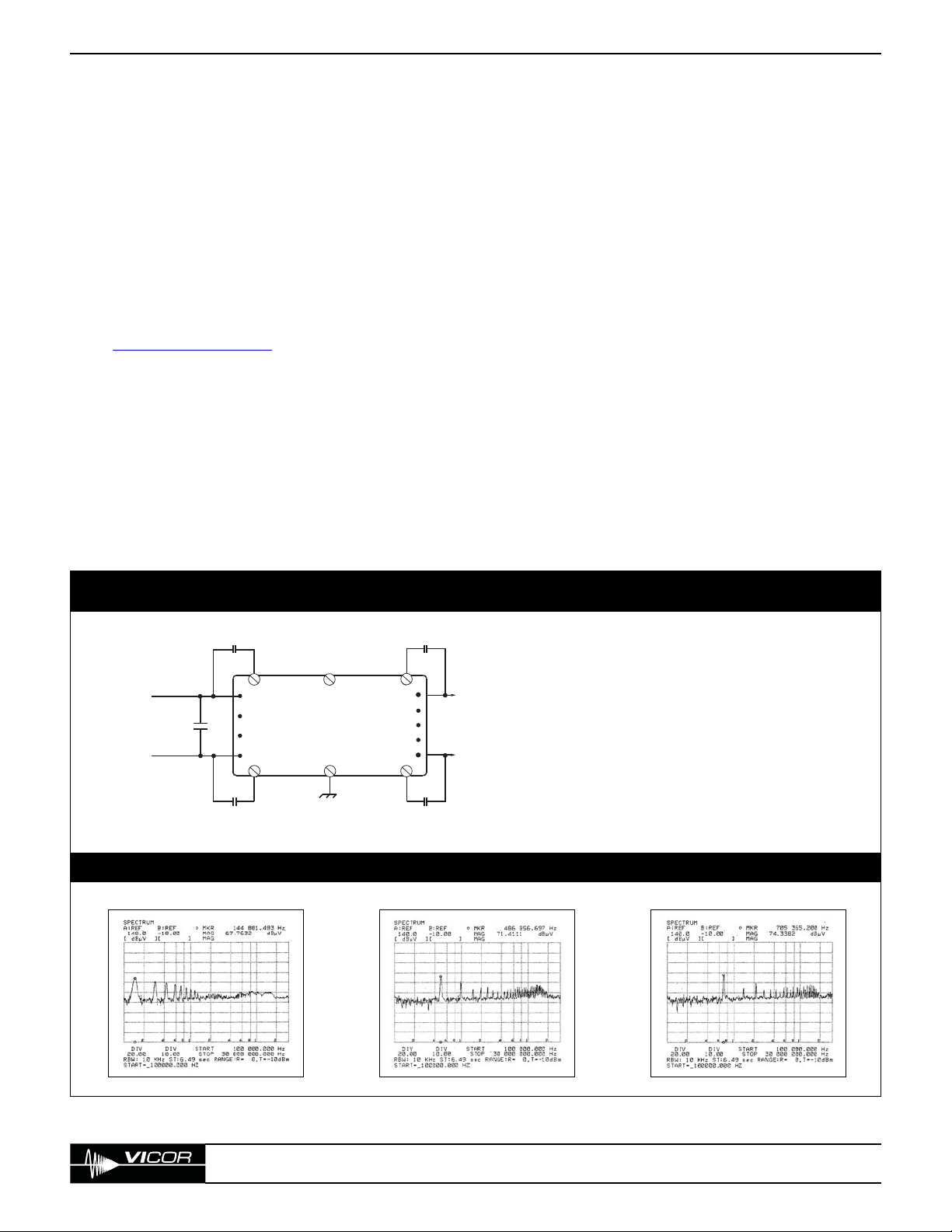
Figure 9–1 — Conducted input noise, no additional filtering
3 Amp Load 15 Amp Load 30 Amp Load
CONDUCTED NOISE
Conducted noise is the AC current flowing between the
source voltage and the power supply. It includes both
common-mode and differential-mode noise. Vicor zerocurrent-switching converters are 20 – 40 dB lower in
conducted noise than a traditional board-mounted PWM
converter; however, if a specific EMC specification such as
FCC or VDE must be met, additional filtering may be required.
Since the noise generated is ten to a hundred times lower
than fixed frequency converters, an existing filter should
provide equal or better performance when the conditions
in the
Module Do’s and Don’ts section are followed.
(Section 3)
In the event the system does not contain an existing filter,
the following will provide valuable information relative to
the attainment of system conducted noise objectives.
System requirements, such as Tempest (military) or UL544 /
EN60601 (medical), require a somewhat different approach.
Medical requirements vary as a function of the application
and country — please contact Vicor Applications
Engineering for additional details.
Common-Mode Noise with No Additional Filtering.
Common mode conducted noise current is the
unidirectional (in phase) component in both the +IN and
–IN pins to the module. This current circulates from the
converter via the power input leads to the DC source and
returns to the converter via the grounded baseplate or
output lead connections. This represents a potentially
large loop cross-sectional area which, if not effectively
controlled, can generate magnetic fields. Common-mode
noise is a function of the dv/dt across the main switch in
the converter and the effective input to baseplate and
input to output capacitance of the converter.
The most effective means to reduce common-mode current
is to bypass both input leads to the baseplate with
Y-capacitors (C2), keeping the leads short to reduce
parasitic inductance. Additionally, a common-mode choke
(L1) is usually required to meet FCC/ VDE A or B. (Figure
9–2)
9. EMC Considerations
Conducted Noise vs. Load
Typical Vicor Module
48 V Input, 5 V Output (VI-230-CV)
+OUT
+S
TRIM
–S
–OUT
C3
C3
Conditions:
C1 = 100 μF
C2 = 4,700 pF
C3 = 0.01 μF
Light Load = 3 A
Nominal Line = 48 V Nominal Load = 15 A
Full Load = 30 A
C1
C2
C2
+IN
GATE
IN
GATE
OUT
–IN
Page 2
Design Guide & Applications Manual
For VI-200 and VI-J00 Family DC-DC Converters and Configurable Power Supplies
vicorpower.com 800-735-6200 Applications Engineering 1-800-927-9474 Rev. 2.1
Page 19 of 88
9. EMC Considerations
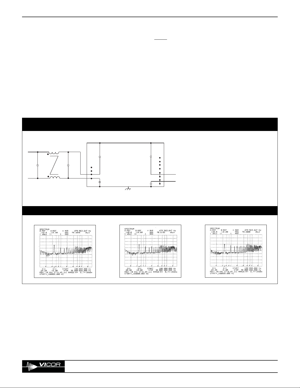
Common-Mode Noise with Common-Mode Choke.
There are no special precautions that must be exercised in
the design of input filters for Vicor converters. In fact, if
the system contains an EMC filter designed for typical
fixed frequency converters, it should be sufficient as is
(although not optimal in terms of size), as zero-currentswitching converters inherently generate significantly less
conducted noise.
The plots in Figure 9–2 are representative of fixed
frequency converters with input filtering.
NOTE: In most cases, a fixed frequency converter
generates more input conducted noise with a filter
than Vicor’s zero-current-switching converter without
a filter. Also note that fixed frequency converters
using a construction technique involving control
circuitry on the same metal plate as power processing
components will generate significantly more input
noise than shown.
Figure 9–2 — Conducted input noise, typical fixed frequency converter with filter
3 Amp Load 15 Amp Load 30 Amp Load
Typical Fixed Frequency Converter (PWM)
48 V Input, 5 V Output
Conducted Noise vs. Load
C3
L1
C1
C2
+IN
–IN
–OUT
+OUT
C4
Conditions:
C1 = 2.2 μF
C2 = 100 μF
C3 = Internal
C4 = Internal
L1 = 3 mH
Nominal Line = 48 V
Light Load = 3 A
Nominal Load = 15 A
Full Load = 30 A
C3
C4
Page 3
Design Guide & Applications Manual
For VI-200 and VI-J00 Family DC-DC Converters and Configurable Power Supplies
vicorpower.com 800-735-6200 Applications Engineering 1-800-927-9474 Rev. 2.1
Page 20 of 88
9. EMC Considerations
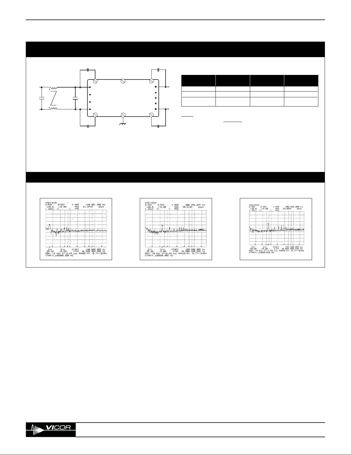
3 Amp Load 15 Amp Load 30 Amp Load
Conducted Noise vs. Load
Figure 9–3 — Conducted input noise, with common-mode choke
Typical Vicor Module (VI-230-CV)
48 V Input, 5 V Output
Three common-mode chokes are offered as standard accessories.
NOTE
: Common-mode filters may be common to one or
more modules, but only one
should be used with modules
interconnected via GATE IN’s or, GATE OUT to GATE IN. As
an example, Driver / Booster arrays or Drivers with GATE IN’s
tied together to provide a common disable function.
Part Inductance Maximum Resistance
Number Each Winding DC Current Each Winding
31743 1,000 µH 12 Amperes 6.5 mΩ
31742 3,000 µH 7 Amperes 18 mΩ
31943 2,163 µH 1 Ampere 42 mΩ
C2
a
L1
C4
C1 = 100 μF
C2a – C2b = 4,700 pF (Vicor Part # 01000)
C3a – C3b = 0.01 μF (Vicor Part # 04872)
C4 = 2.2 μF
L1 = 3,000 μH (Vicor Par t # 31742)
C1
C2
+IN
GATE
IN
GATE
OUT
–IN
b
C3
a
+OUT
+S
TRIM
–S
–OUT
C3
b
Conditions
Light Load = 3 A
Nominal Load = 15 A
Full Load = 30 A
Page 4

Design Guide & Applications Manual
For VI-200 and VI-J00 Family DC-DC Converters and Configurable Power Supplies
vicorpower.com 800-735-6200 Applications Engineering 1-800-927-9474 Rev. 2.1
Page 21 of 88
9. EMC Considerations
Differential and Common-Mode Filter with More
than One Module. No special precautions are needed
when using two or more modules. The filter required will
have the same characteristics as a single module filter,
however the wire size on the magnetics will need to
reflect the increased input current. Shown below is the
input conducted noise for two modules sharing a
common input source.
Figure 9–4 — Conducted noise, multiple zero-current-switching converters
3 Amp / 3 Amp Load
3 Amp / 6 Amp Load
15 Amp / 15 Amp Load
3 Amp / 30 Amp Load
15 Amp / 30 Amp Load 30 Amp / 30 Amp Load
Differential and Common-Mode Filter with More than One Module
48 V Inputs, 5 V Outputs (Two Vicor VI-230-CV Modules)
Conducted Noise vs. Load
Three common-mode chokes are offered as standard accessories.
NOTE
: Common-mode filters may be common to one or
more modules, but only one should be used with modules
interconnected via GATE IN’s or, GATE OUT to GATE IN. As
an example, Driver / Booster arrays or Drivers with GATE IN’s
tied together to provide a common disable function.
Part Inductance Maximum Resistance
Number Each Winding DC Current Each Winding
31743 1,000 µH 12 Amperes 6.5 mΩ
31742 3,000 µH 7 Amperes 18 mΩ
31943 2,163 µH 1 Ampere 42 mΩ
C2
a
L2C4L1
C1
a
C1
C1a – C1b = 47 μF
C2a – C2d = 4,700 pF (Vicor Part # 01000)
C3a – C3d = 0.01 μF (Vicor Part # 04872)
C4 = 2.2 μF
L1 = 3,000 μH (Vicor Part # 31742)
L2 = 20 μH
+IN
GATE
IN
GATE
OUT
–IN
C2
b
C2
c
+IN
GATE
IN
b
GATE
OUT
–IN
C2
d
C3
a
+OUT
+S
T
–S
–OUT
C3
b
C3
c
+OUT
+S
T
–S
–OUT
C3
d
Conditions
Light Load = 3 A
Nominal Load = 15 A
Full Load = 30 A
Load 1
Load 2
Page 5

Design Guide & Applications Manual
For VI-200 and VI-J00 Family DC-DC Converters and Configurable Power Supplies
vicorpower.com 800-735-6200 Applications Engineering 1-800-927-9474 Rev. 2.1
Page 22 of 88
3 Amp Load 15 Amp Load 30 Amp Load
9. EMC Considerations
Differential-Mode Noise Filter. Differential-mode
conducted noise current is the component of current,
at the input power pin, which is opposite in direction or
phase with respect to the other input power pin.
All Vicor converters have an internal differential-mode LC
filter which, in conjunction with a small external capacitor
C1 (minimum value in µF) = 400 / Vin,
reduces differential-mode conducted noise. The external
capacitor should be placed close to the module to reduce
loop cross-sectional area.
Care should be taken to reduce the loop cross-sectional
area of differential-mode current flowing between the
source and C1. Since differential-mode input current is by
definition opposite in phase, twisting the input leads
causes noise cancellation. PCB power planes can reduce
radiated noise if the traces are on opposite sides of the
PCB directly over one another. If differential mode inductance
is used, it may be common to one or more modules.
C2
a
C1
C2
b
C3
b
C3
a
L1
C4
L2
C1 = 100 µF
C2a – C2b = 4,700 pF (Vicor Part # 01000)
C3a – C3b = 0.01 µF (Vicor Part # 04872)
C4 = 2.2 µF
L1 = 20 µH
L2 = 20 µH
+IN
GATE
IN
GATE
OUT
–IN
+OUT
+S
TRIM
–S
–OUT
Conditions
Light Load = 3 A
Nominal Load = 15 A
Full Load = 30 A
Figure 9–5 — Conducted noise, differential-mode filtering
Conducted Noise vs. Load
Differential-Mode Filter
Typical Vicor Module (VI-230-CV) 48 V Input, 5 V Output
Page 6

Design Guide & Applications Manual
For VI-200 and VI-J00 Family DC-DC Converters and Configurable Power Supplies
vicorpower.com 800-735-6200 Applications Engineering 1-800-927-9474 Rev. 2.1
Page 23 of 88
9. EMC Considerations
RADIATED NOISE
Radiated noise may be either electric field or magnetic
field. Magnetic radiation is caused by high di/dt and is
generally what is measured by FCC, VDE or MIL-STD-461.
Vicor converters utilize zero-current-switching, with the
advantage over PWM non-zero-current-switching being
that zero-current-switching topologies contain minimal
discontinuities in the switched current waveforms,
resulting in lower di/dt’s. Electric field radiation (caused by
dv/dt) is “near-field,” i.e., it decays rapidly as a function of
distance and as a result does not typically affect radiated
measurements.
Radiation can be minimized by proper board layout. Keep
all leads with AC current short, twisted or routed as
overlapping planes to minimize loop cross-sectional area.
Also keep in mind the effects of capacitive coupling —
even when not expected. Do not put an unshielded filter
on the opposite side of the PCB from the module.
Conducted noise can be capacitively coupled around the
filter. Do not route input and output leads in the same
cable bundle. Again, no special precautions, just good
design practice.
NOISE CONSIDERATIONS
All switchmode power supplies generate a certain amount
of “noise”, yet it remains one of the least understood
parameters in power conversion.
VI-200s and VI-J00s both use the same topology, so their
operation is very similar. These products are zero-currentswitching converters — i.e., the current is zero when the
main switch is turned on or off. While the switch is on,
the current through the switch or the primary of the
transformer is a half-wave rectified sine wave. Similar in
operation to a resonant converter, these products are
commonly referred to as quasi-resonant converters. The
LC resonant frequency is fixed so the on-time of the
switch is about 500 ns. When the switch turns on, energy
builds up in the leakage inductance of the transformer (L)
and then “transferred” into the capacitor on the
secondary side of the module. (C, Figure 9–6) The energy
processed in each pulse is fixed, and is ultimately the
energy stored in this capacitor, 1/2 CV
2
. Since the energy
in every pulse is fixed, the repetition rate of the pulse train
is varied as a function of load to regulate the output
voltage. Maximum repetition rate occurs at minimum line,
full load and is approximately twice the LC time period or
1 µs. If the load drops by 50%, then the repetition rate is
approximately one-half of maximum (since the energy in
every pulse is fixed). Therefore the pulse repetition rate
varies linearly with load, to a first order approximation.
Since the energy in every pulse is related to the square of
the applied voltage (CV
2
), the pulse repetition rate varies
as approximately the square of the line voltage. For
example, a 300 V input unit can vary from 200 – 400 V,
or a factor of two, therefore it follows that the repetition
rate must vary by approximately a factor of four to regulate
the output. As previously established, the current in the
primary is a half-wave rectified sine wave, but the voltage
on the primary is a square wave. Since this voltage is a
square wave, it contains harmonics of the fundamental
switching frequency. It also includes frequencies, that extend
to 70 MHz.
These frequencies can be of interest in the following
circumstances. Rapidly changing voltages (high dv/dt) can
generate E-fields (primarily near-field) which do not usually
cause system noise problems since they significantly
decrease as a function of distance. For this reason, E-fields
are not measured by agencies such as the FCC or VDE.
These agencies do, however, measure the magnetic
radiation caused by high frequency currents in a conductor.
The half-wave rectified sine wave in the transformer is an
example of this, but since there are minimal discontinuities
in the current waveform and the loop cross-sectional area
is very small, the resultant E-field is very small. E-fields can
be a problem if sensitive circuitry is located near the
module. In this case, a shield can be positioned under the
label side of the module as a discrete element or as a
ground plane on the PCB. The other effect that occurs as
a result of the 50 – 70 MHz component on the main
switch is common-mode noise. (Figure 9–7)
Figure 9–6 — Basic zero-current-switching converter topology
(VI-200 / VI-J00)
Figure 9–7 — The shield layer serves to reduce the capacitance
Vs
+IN
Vp
–IN
L
+ OUT
C
Ip
–OUT
Parasitic
Capacitance
FET
Ceramic
Baseplate
Rectifier
ShieldShield
Ceramic
Page 7

Design Guide & Applications Manual
For VI-200 and VI-J00 Family DC-DC Converters and Configurable Power Supplies
vicorpower.com 800-735-6200 Applications Engineering 1-800-927-9474 Rev. 2.1
Page 24 of 88
Figure 9–8 — Noise coupling model
9. EMC Considerations
To Scope
Ground Ring on Probe
To Scope
or
Insert probe into female receptacle
(Vicor P/N 06207) for proper output
differential noise measurement technique
Figure 9–9 — Output ripple measurement technique
The dv/dt of the switch (FET) is a noise generator. This
FET is mounted on a two layer insulating and shielding
assembly which is attached to the baseplate. Since ceramic
is a dielectric, there is capacitance from the FET to the
baseplate. (Figure 9–7) The output rectifiers are also tied
to the baseplate with ceramic insulators, adding additional
capacitance. The dv/dt of the FET is differentiated by these
two series capacitors, resulting in a spike of noise current
at 50 – 70 MHz that flows from primary to secondary.
(Figure 9– 8) This noise current is common-mode as opposed
to differential, and therefore should not affect the operation
of the system. It should be noted, however, that oscilloscopes
have a finite ability to reject common-mode signals, and
these signals can be abnormally emphasized by the use of
long ground leads on the scope probe.
MEASURING OUTPUT NOISE
Long ground leads adversely impact the common-mode
rejection capability of oscilloscopes because the ground
lead has inductance not present on the signal lead. These
differing impedances take common-mode signals and
convert them to differential signals that show up on the
trace. To check for common-mode noise, place the
oscilloscope probe on the ground lead connection of the
probe while the ground lead is tied to output return.
(Figure 9–9) If the noise is common-mode, there will still
be “noise” observed at the same test point.
NOTE
: The output return must be at the same relative
potential as the earth ground of the oscilloscope or
damaging current may flow through the oscilloscope
ground lead.
Capacitors are required from the +/–IN to the baseplate
thereby shunting common-mode current, thus reducing
noise current on the input power lines. The capacitor must
have very short leads since the frequency is high. It must
also be a good capacitor (i.e., ceramic or other material
that has a low ESR / ESL). This type of capacitor is most
important on high input voltage units since the “dv”
is larger, but is required for all units. For off-line
applications this capacitor must have the appropriate
safety agency approvals.
A capacitor from +/–Vout to the baseplate, is required
since the output rectifier has a changing voltage on it,
and, like the FET, can generate common-mode noise.
This capacitor is similarly recommended for high output
voltage units (48 V).
Common-mode noise is not differential with respect to
the output. It does, however, flow in both input and
output leads of the power supply and is a noise parameter
that is measured by the FCC or VDE. It can cause power
systems to fail radiated emission tests, so it must be dealt
with. Bypass capacitors to the baseplate with a commonmode filter on the input of the module or the main input
of the power supply is required.
The common-mode filter is typically placed on the input as
opposed to the output. Theoretically, since this current
flows from primary to secondary, the choke could be
placed in either the input or the output, but is preferably
placed in the input leads for the following reasons:
1) input currents are smaller since the input voltage is
usually higher;
2) line regulation of the module can correct for voltage
drops across the choke; and
3) if the choke is on the output and the senses are
connected to the other side of it, the stability of the
loop may be impacted.
Differential output noise is the AC component of the
output voltage that is not common to both outputs. The
noise is comprised of both low frequency, line-related
noise (typically 120 Hz) and high frequency switching noise.
V
p
I
CM
Primary Secondary
V
p
I
V
p
Baseplate
C
FET
I
CM
C
FET
DM
C
External
Ycaps Ycaps
C
Rectifier
C
Rectifier
C
External
Page 8

Design Guide & Applications Manual
For VI-200 and VI-J00 Family DC-DC Converters and Configurable Power Supplies
vicorpower.com 800-735-6200 Applications Engineering 1-800-927-9474 Rev. 2.1
Page 25 of 88
9. EMC Considerations
No Additional Filter 2% p-p (Typical) 1% p-p (Typical) 0.2% p-p (Typical)
Low ESR Output Cap. 1% p-p (Typical) 0.5% p-p (Typical) 0.1% p-p (Typical)
LC Output Filter 0.4% p-p (Typical) 0.2% p-p (Typical) 0.05% p-p (Typical)
RAM Filter (VI-200) <3 mV p-p (Maximum) <3 mV p-p (Maximum) <3 mV p-p (Maximum)
RAM Filter (VI-J00) <10 mV (Maximum) <10 mV (Maximum) <10 mV (Maximum)
Table 9–1 — Output filter options and output voltage and ripple
3 Amp Load 15 Amp Load 30 Amp Load
High Frequency Switching Noise. Peak-to-peak output
voltage ripple is typically 2% or less (1% for 12 V outputs
and above). Hence additional output filtering is generally
not required. Digital systems rarely need additional
filtering. However some analog systems, such as
ultrasound systems, will probably require additional output
filtering. See additional output filter choices in Table 9–1.
Line Related Output Noise. Line related output noise
can be determined from the converter specification —
Input Ripple Rejection. As an example, a VI-260-CV
(300 Vin to 5 Vout) has a rejection specification at 120 Hz
of 30 + 20 Log (Vin / Vout). Vin = 300 and Vout = 5,
hence its rejection is 30 + 35.56 = 65.56 dB, which
provides an attenuation factor of 1.89 k. Therefore, if the
input to the converter has 30 V p-p of ripple, the output
p-p ripple would be 15.8 mV. It is not practical to
attenuate this component further with passive filtering
due to its low frequency, hence active filtering is required.
The RAM contains both a passive filter for high frequency
noise and an active filter for low frequency noise.
Figure 9–10 — Output noise, no additional output filtering
Output Ripple vs. Load
Differential Output Filtering
Typical Vicor Module (VI-230-CV) 48 V Input, 5 V Output
5 V Outputs 12 – 15 V Outputs 24 – 48 V Outputs
C1
C2
C2
a
b
+IN
GATE
OUT
GATE
IN
–IN
+OUT
+S
TRIM
–S
–OUT
C3
C3
a
C1 = 100 µF
C2a – C2b = 4,700 pF (Vicor Part # 01000)
C3a – C3b = 0.01 µF (Vicor Part # 04872)
b
Conditions
Light Load = 3 A
Nominal Load = 15 A
Full Load = 30 A
Page 9

Design Guide & Applications Manual
For VI-200 and VI-J00 Family DC-DC Converters and Configurable Power Supplies
vicorpower.com 800-735-6200 Applications Engineering 1-800-927-9474 Rev. 2.1
Page 26 of 88
9. EMC Considerations
NOTE: A low ESR capacitor should be used on the output, preferably tantalum.
3 Amp Load 15 Amp Load 30 Amp Load
Figure 9–11 — Output noise, additional output capacitance
Output Ripple vs. Load
Addition of Output Capacitor
Typical Vicor Module (VI-230-CV) 48 V Input, 5 V Output
+OUT
+S
TRIM
–S
–OUT
C3
C3
a
C1 = 100 µF
C4
b
C2a – C2b = 4,700 pF (Vicor Part # 01000)
C3a – C3b = 0.01 µF (Vicor Part # 04872)
C4 = 270 µF (Tant.)
C1
C2
C2
a
b
+IN
GATE
IN
GATE
OUT
–IN
Conditions
Light Load = 3 A
Nominal Load = 15 A
Full Load = 30 A
Page 10

Design Guide & Applications Manual
For VI-200 and VI-J00 Family DC-DC Converters and Configurable Power Supplies
vicorpower.com 800-735-6200 Applications Engineering 1-800-927-9474 Rev. 2.1
Page 27 of 88
9. EMC Considerations
Figure 9–12 — Output noise, additional output inductor and capacitor (L-C Filter)
Output Ripple vs. Load
LC Output Filter
Typical Vicor Module (VI-230-CV) 48 V Input, 5 V Output
3 Amp Load 15 Amp Load 30 Amp Load
C1
C2
C2
a
b
+IN
GATE
IN
GATE
OUT
–IN
+OUT
+S
TRIM
–S
–OUT
C3
C3
a
L1
C4
b
C1 = 100 µF
C2a – C2b = 4,700 pF (Vicor Part # 01000)
C3a – C3b = 0.01 µF (Vicor Part # 04872)
C4 = 270 µF (Tant.)
L1 = 200 nH (Vicor Part # 30268)
Conditions
Light Load = 3 A
Nominal Load = 15 A
Full Load = 30 A
Page 11

Design Guide & Applications Manual
For VI-200 and VI-J00 Family DC-DC Converters and Configurable Power Supplies
vicorpower.com 800-735-6200 Applications Engineering 1-800-927-9474 Rev. 2.1
Page 28 of 88
9. EMC Considerations
RAM / MI-RAM OPERATION
The RAM/ MI-RAM attenuates output noise in two ways.
First, an LC filter in the RAM/ MI-RAM attenuates high
frequency components associated with the switching
frequency. Secondly, the RAM/ MI-RAM contains an active
filter that attenuates low frequency components associated
with the input to the converter. These frequencies are on
the order of 60 – 120 Hz and harmonics would require
very large output LC if a passive approach were to be
used. Essentially, the active circuit looks at the output
ripple from the converter, multiplies it by –1 (inverts) and
adds it to the output. This effectively cancels out the low
frequency components.
The RAM does not contain any common-mode filtering,
so whatever common-mode noise is present is passed
through. It only provides differential filtering of noise that
is present on one output pin relative to the other.
The use of the RAM/ MI-RAM is very straightforward, but
a couple of precautions should be noted. The LC filter is in
the positive output lead, so if that lead is shorted then the
high frequency attenuation is compromised. The active
circuit is in the negative output lead, so if that lead is
shorted the low frequency attenuation is compromised.
The RAM must be used with a common-mode choke at
the input of the converter.
The RAM is intended to be used with the Vicor VI-200/
VI-J00, and the MI-RAM is intended to be used with Vicor
MI-200/ MI-J00 Family of DC-DC converter modules. It is
also available in a chassis mounted version as VI-LRAM-xx
(MegaMod package) or VI-RAM-xx-B1 (BusMod package).
NOTE
: Do not use if load is inductive as instability
may result. The addition of the RAM will increase the
converter’s current limit setpoint by ~ 14%.
3 Amp Load 15 Amp Load
30 Amp Load
(Overload Condition)
Figure 9–13 — Output noise, with Ripple Attenuator Module (RAM)
Output Ripple vs. Load
RAM Output Filter
Typical Vicor Module (VI-230-CV) 48 V Input, 5 V Output with VI-RAM-C2
C2
a
C3
a
L1
+
C1
–
C2
b
+IN
GATE
IN
GATE
OUT
–IN
+OUT
+S
TRIM
–S
–OUT
C3
C4
b
+IN
+OUT
+S IN
–S IN
+
–IN
+S
RAM
–S
–OUT
C1 = 100 µF
C2a – C2b = 4,700 pF (Vicor Part # 01000)
C3a – C3b = 0.01 µF (Vicor Part # 33643)
C4 = 220 µF (Electrolytic)
Conditions
Light Load = 3 A
Full Load = 15 A
Overload Condition = 30 A
 Loading...