

Page 1
ADL Embedded Solutions GmbH, Eiserfelder Str. 316, ADL Embedded Solutions Inc. 4411 Morena Blvd., Suite 101
57080 Siegen, Germany San Diego, CA 92117-4345
P. +49 (0) 271 250 810 0 F. +49 (0) 271 250 810 20 P. +1 858 490-0597 F. +1 858 490-0599
e-mail: sales@adl-europe.com; web: http://www.adl-europe.com e-mail: sales@adl-usa.com; web: http://www.adl-usa.com
ADLE3800PC
Manual
rev. 1.0
Page 2

Page 3

Contents
Beckhoff New Automation Technology ADLE3800PC page 3
Contents
0 Document History................................................................................................................................. 6
1 Introduction .......................................................................................................................................... 7
1.1 Important Notes ............................................................................................................................ 7
1.2 Technical Support ......................................................................................................................... 7
1.3 Warranty ....................................................................................................................................... 7
1.4 Return Authorization ..................................................................................................................... 7
1.5 Description of Safety Symbols ...................................................................................................... 8
1.6 RoHS ............................................................................................................................................ 8
1.7 FCC Approval for Canada ............................................................................................................ 8
1.8 FCC Approvals for the United States of America ......................................................................... 8
2 Overview ............................................................................................................................................ 10
2.1 Features ...................................................................................................................................... 10
2.1.1 Specifications and Documents ........................................................................................... 11
3 Connectors ......................................................................................................................................... 12
3.1 Connector Map ........................................................................................................................... 13
3.2 Power Supply .............................................................................................................................. 14
3.3 System/SM-Bus .......................................................................................................................... 15
3.4 Memory ....................................................................................................................................... 16
3.5 PCI/104-Express Bus ................................................................................................................. 19
3.6 PCI-Express Mini Card with mSATA .......................................................................................... 21
3.7 DVI/HDMI/VGA ........................................................................................................................... 22
3.8 DisplayPort.................................................................................................................................. 23
3.9 USB 2.0 ....................................................................................................................................... 24
3.10 USB 3.0 ....................................................................................................................................... 25
3.11 LAN ............................................................................................................................................. 26
3.12 Audio ........................................................................................................................................... 27
3.13 SATA Interfaces .......................................................................................................................... 28
3.14 COM1 and COM2 ....................................................................................................................... 29
3.15 GPIO ........................................................................................................................................... 30
3.16 Monitoring Functions .................................................................................................................. 31
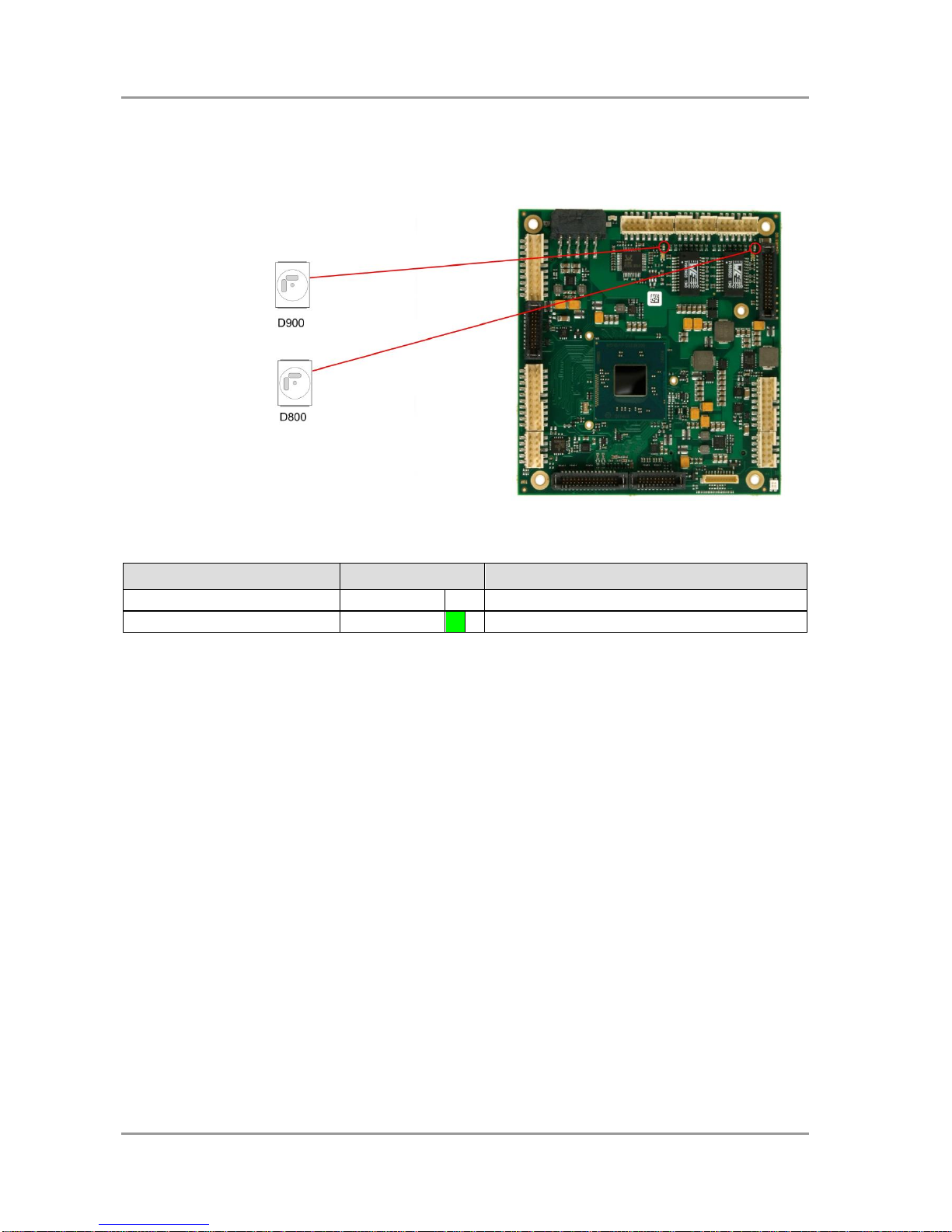
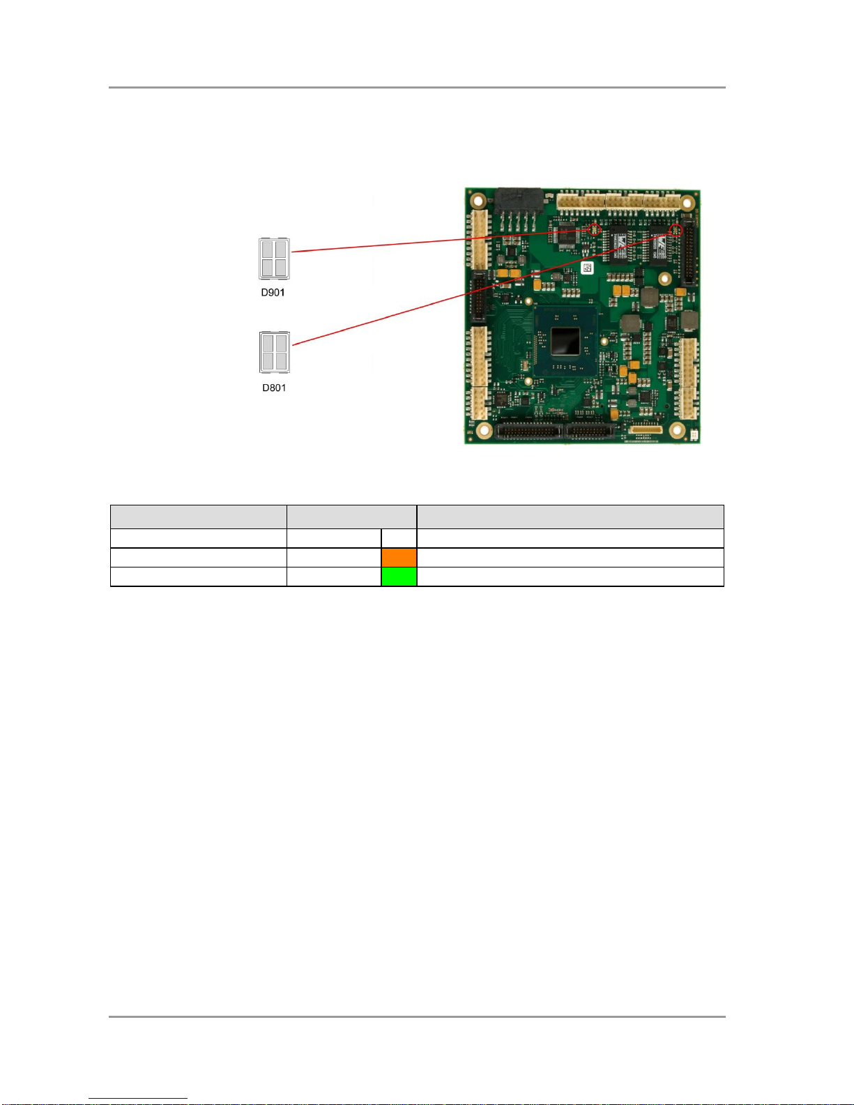
4 State LEDs ......................................................................................................................................... 32
4.1 HD LED ....................................................................................................................................... 32
4.2 RGB LED .................................................................................................................................... 33
4.3 LAN Activity LED ........................................................................................................................ 34
4.4 LAN Speed LED ......................................................................................................................... 35
5 BIOS Settings ..................................................................................................................................... 36
5.1 General Remarks ........................................................................................................................ 36
5.2 Main ............................................................................................................................................ 37
5.3 Advanced .................................................................................................................................... 38
5.3.1 ACPI Settings...................................................................................................................... 40
5.3.2 H/W Monitor ........................................................................................................................ 41
5.3.3 CPU Configuration .............................................................................................................. 43
5.3.4 PPM Configuration .............................................................................................................. 47
5.3.5 SATA Configuration ............................................................................................................ 48
5.3.6 Miscellaneous Configuration ............................................................................................... 49
5.3.7 LPSS & SCC Configuration ................................................................................................ 50
Page 4

Contents
page 4 Beckhoff New Automation Technology ADLE3800PC
5.3.8 Network Stack ..................................................................................................................... 52
5.3.9 Power Controller Options .................................................................................................... 53
5.3.10 CSM Configuration ............................................................................................................. 55
5.3.11 SDIO Configuration ............................................................................................................. 56
5.3.12 USB Configuration .............................................................................................................. 57
5.3.13 Security Configuration ........................................................................................................ 58
5.4 Chipset ........................................................................................................................................ 59
5.4.1 North Bridge ........................................................................................................................ 60
5.4.2 South Bridge ....................................................................................................................... 64
5.5 Security ....................................................................................................................................... 68
5.5.1 Secure Boot menu .............................................................................................................. 69
5.6 Boot ............................................................................................................................................. 72
5.7 Save & Exit ................................................................................................................................. 73
5.8 BIOS Update ............................................................................................................................... 74
6 Mechanical Drawings ......................................................................................................................... 75
6.1 PCB: Mounting Holes ................................................................................................................. 75
6.2 PCB: Pin 1 Dimensions - Top ..................................................................................................... 76
6.3 PCB: Pin 1 Dimensions - Bottom ................................................................................................ 77
6.4 PCB: Heat Sink/Die Center ......................................................................................................... 78
6.5 Heat Spreader: Chassis Mount................................................................................................... 79
7 Technical Data ................................................................................................................................... 80
7.1 Electrical Data ............................................................................................................................. 80
7.2 Environmental Conditions ........................................................................................................... 80
7.3 Thermal Specifications ............................................................................................................... 81
I Annex: Post-Codes ............................................................................................................................ 83
II Annex: Resources .............................................................................................................................. 84
IO Range ................................................................................................................................................ 84
Memory Range ....................................................................................................................................... 84
Interrupt .................................................................................................................................................. 84
PCI Devices ............................................................................................................................................ 85
SMB Devices .......................................................................................................................................... 85
Page 5

Important Notes Chapter: Document History
ADL Embedded Solutions ADLE3800PC page 5
Page 6

Chapter: Document History Important Notes
page 6 ADL Embedded Solutions ADLE3800PC
0 Document History
Version
Changes
0.1
first pre-release
1.0
first complete version
All company names, brand names, and product names referred to in this manual are registered or
unregistered trademarks of their respective holders and are, as such, protected by national and
international law.
Page 7

Important Notes Chapter: Introduction
ADL Embedded Solutions ADLE3800PC page 7
1 Introduction
1.1 Important Notes
Please read this manual carefully before you begin installation of this hardware device. To avoid
Electrostatic Discharge (ESD) or transient voltage damage to the board, adhere to the following rules at
all times:
o You must discharge your body from electricity before touching this board.
o Tools you use must be discharged from electricity as well.
o Please ensure that neither the board you want to install, nor the unit on which you want to install this
board, is energized before installation is completed.
o Please do not touch any devices or components on the board.
As soon as the board is connected to a working power supply, touching
the board may result in electrical shock, even if the board has not been
switched on yet. Please also note that the mounting holes for heat sinks
are connected to ground, so when using an externally AC powered device, a substantial ground
plane differential can occur if the external device's AC power supply or cable does not include an
earth ground. This could also result in electrical shock when touching the device and the heat
sink simultaneously.
1.2 Technical Support
Technical support for this product can be obtained in the following ways:
o By contacting our support staff at +1 858-490-0597 or +49 (0) 271 250 810 0
o By contacting our staff via e-mail at support@adl-usa.com or support@adl-europe.com
o Via our website at www.adl-usa.com/support or www.adl-europe.com/support
1.3 Warranty
This product is warranted to be free of defects in workmanship and material. ADL Embedded Solutions'
sole obligation under this warranty is to provide replacement parts or repair services at no charge, except
shipping cost. Such defects which appear within 12 months of original shipment of ADL Embedded
Solutions will be covered, provided a written claim for service under warranty is received by ADL
Embedded Solutions no less then 30 days prior to the end of the warranty period of within 30 days of
discovery of the defect – whichever comes first. Warranty coverage is contingent upon proper handling
and operation of the product. Improper use such as unauthorized modifications or repair, operation
outside of specified ratings, or physical damage may void any service claims under warranty.
1.4 Return Authorization
All equipment returned to ADL Embedded Solutions for evaluation, repair, credit return, modification, or
any other reason must be accompanied by a Return Material Authorization (RMA) number. ADL
Embedded Solutions requires a completed RMA request form to be submitted in order to issue an RMA
number. The form can be found under the Support section at our website: www.adl-usa.com or
www.adl-europe.com. Submit the completed form to support@adl-usa.com or fax to +1 858-490-0599 for
the USA office, or to rma@adl-europe.com or fax to +49 (0) 271 250 810 20 to request an RMA from the
European office in Germany. Following a review of the information provided, ADL Embedded Solutions
will issue an RMA number.
WARNING
Page 8

Chapter: Introduction Description of Safety Symbols
page 8 ADL Embedded Solutions ADLE3800PC
1.5 Description of Safety Symbols
The following safety symbols are used in this documentation. They are intended to alert the reader to the
associated safety instructions.
DANGER indicates a hazardous situation which, if not avoided, will
result in death or serious injury.
WARNING indicates a hazardous situation which, if not avoided, could
result in death or serious injury.
CAUTION indicates a hazardous situation which, if not avoided, could
result in minor or moderate injury.
NOTICE is used to address practices not related to physical injury.
1.6 RoHS
The PCB and all components are RoHS compliant (RoHS = Restriction of Hazardous Substances
Directive). The soldering process is lead free.
1.7 FCC Approval for Canada
FCC: Canadian Notice
This equipment does not exceed the Class A limits for radiated emissions as described in the Radio
Interference Regulations of the Canadian Department of Communications.
1.8 FCC Approvals for the United States of America
FCC: Federal Communications Commission Radio Frequency Interference Statement
This equipment has been tested and found to comply with the limits for a Class A digital device, pursuant
to Part 15 of the FCC Rules. These limits are designed to provide reasonable protection against harmful
interference when the equipment is operated in a commercial environment. This equipment generates,
uses, and can radiate radio frequency energy and, if not installed and used in accordance with the
instruction manual, may cause harmful interference to radio communications. Operation of this equipment
in a residential area is likely to cause harmful interference in which case the user will be required to
correct the interference at his own expense.
DANGER
WARNING
CAUTION
NOTICE
Page 9

FCC Approvals for the United States of America Chapter: Introduction
ADL Embedded Solutions ADLE3800PC page 9
Page 10
Chapter: Overview Features
page 10 ADL Embedded Solutions ADLE3800PC
2 Overview
2.1 Features
The ADLE3800PC is a highly complex motherboard in the PC/104™ form factor, complying with the
state-of-the-art "PCIe/104™" standard. It's based on a System-On-Chip (SoC) of Intel®'s Atom E3800
product family. Modern low voltage DDR3 technology provides top-notch memory performance,
accomodating up to 8 GByte of RAM (DDR3L-1600) via SO-DIMM204. PCI-Express is available through
the PCI/104-Express Type 2 connector, offering two x1 lanes for connecting all kinds of corresponding
expansion cards in a PCIe/104™ stack-down fashion. For connecting graphics devices, several interfaces
are available: CRT, HDMI and DisplayPort. Additional interfaces include two serial ports, two Gigabit
Ethernet interfaces (LAN), two SATA channels (up to 3Gb/s), an audio interface (HDA 7.1), eight USB2.0channels and one USB3.0-channels. There are also 16 discrete programmable GPIO signals available.
1x
SoDIMM204
DDR3L-
1333
MEMORY
Power VCCCore;
DDRVTT; GFXVCC;
1.05V; 1.5V; 1.8V; 3.3V
BIOS
SATA1-2
RealTek®
ALC889
HDA Link
USB 2, 3, 5 & 6
1.5GB/3.0GB
Intel®
i210
LAN1
10/100/1000
SMBus
SPI
NXP®
PCA9535
SMBus
16x GPIO
MIC 1/2
5.1 Audio
AUX l/r
SPDIF i/o
PIC3
(24FJ256GB210)
FAN
DVI/HDMI
DVI/HDMI/DP
P
C
Ie
(x1
)
Intel® Atom™
E3827, E3845,
E3815
USB1
USB2.0
PCIe/104 connector (type 2)
PCIe Mini Card
1x mSATA, 1x USB2.0
Intel®
i210
10/10
0/100
0
LAN2
USB2.0
USB3.0
SMBus
COM 1-2
LPC
2x USB
2x (1x) PCIe x1
Page 11

Features Chapter: Overview
ADL Embedded Solutions ADLE3800PC page 11
2.1.1 Specifications and Documents
In making this manual and for further reading of technical documentation, the following documents,
specifications and web-pages were used and are recommended.
PC/104™ Specification
Version 2.5
www.pc104.org
PC/104-Plus™ Specification
Version 2.0
www.pc104.org
PCI/104-Express™ Specification
Version 2.01
www.pc104.org
PCI Specification
Version 2.3 and 3.0
www.pcisig.com
ACPI Specification
Version 5.0
www.acpi.info
ATA/ATAPI Specification
Version 7 Rev. 1
www.t13.org
USB Specifications
www.usb.org
SM-Bus Specification
Version 2.0
www.smbus.org
Intel® Chipset Description
Intel® 8 Series Chipset Datasheet
www.intel.com
Intel® Chip Description
i210 Datasheet
www.intel.com
Realtek® Chip Description
ALC885/889 Datasheet
www.realtek.com.tw
Chrontel® Chip Description
Chrontel 7318C Datasheet
www.chrontel.com
American Megatrends®
Aptio™ Text Setup Environment (TSE) User Manual
www.ami.com
American Megatrends®
Aptio™ 4.x Status Codes
www.ami.com
Page 12

Chapter: Connectors Features
page 12 ADL Embedded Solutions ADLE3800PC
3 Connectors
This section describes all the connectors found on the ADLE3800PC.
Page 13
Connector Map Chapter: Connectors
ADL Embedded Solutions ADLE3800PC page 13
3.1 Connector Map
Please use the connector map below for quick reference. Only connectors on the component side are
shown. For more information on each connector refer to the table below.
Ref.-No.
Function
Page
P500
"SATA Interfaces"
p. 28
P501
"USB 3.0"
p. 25
P700/2
"COM1 and COM2"
p. 29
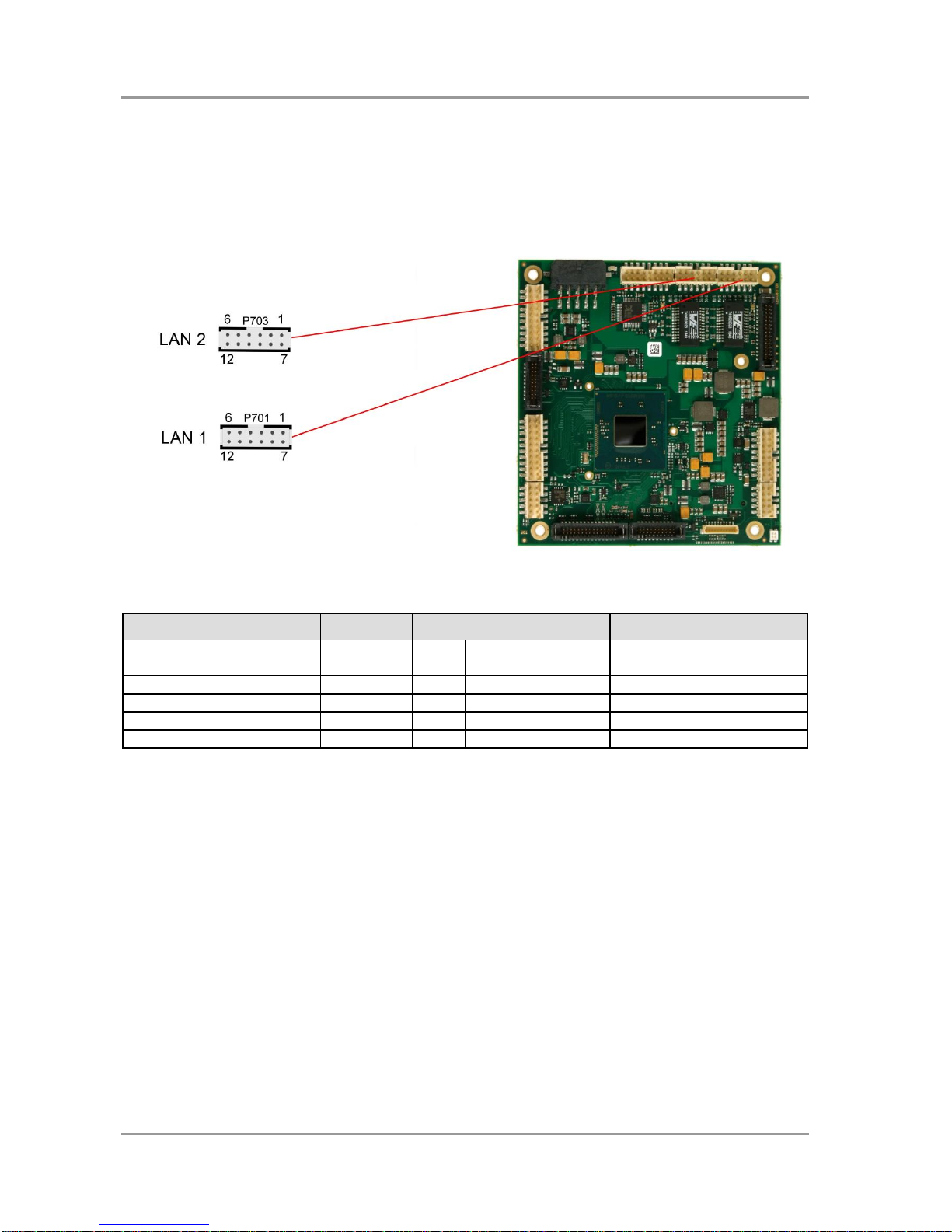
P701/3
"LAN"
p. 26
P704
"Audio"
p. 27
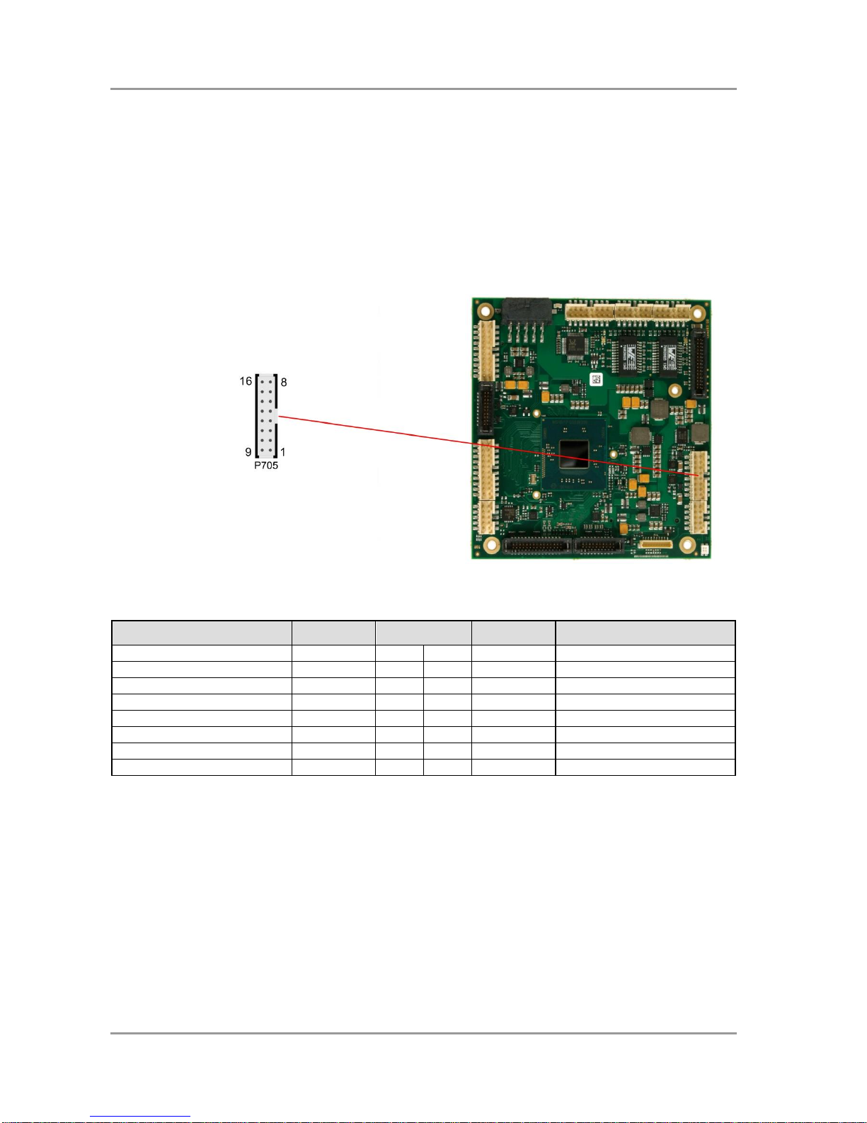
P705
"USB 2.0"
p. 24
P1200
"DVI/HDMI/VGA"
p. 22
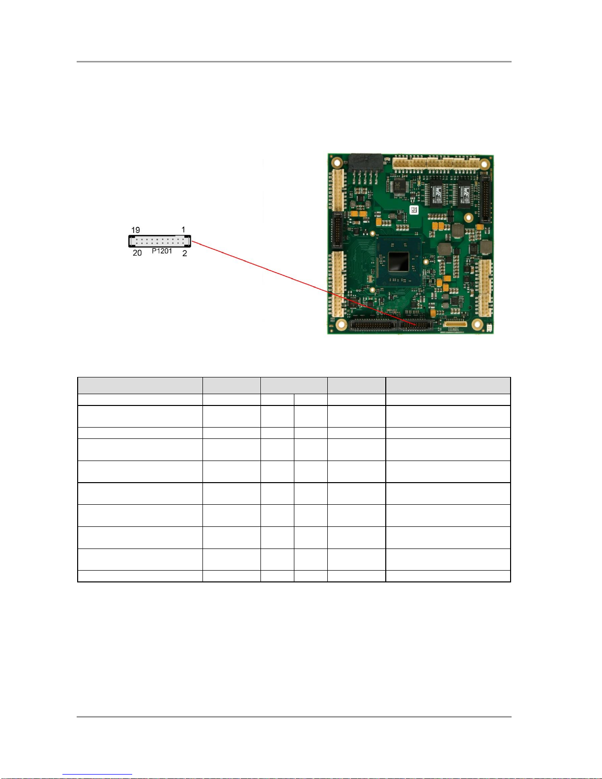
P1201
"DisplayPort"
p. 23
P1300
"GPIO"
p. 30
P1301
"Power Supply"
p. 14
P1302
"System/SM-Bus"
p. 15
P1303
"Monitoring Functions"
p. 31
U600*
"Memory"
p. 16
P1100*
"PCI/104-Express Bus"
p. 19
P1101*
"PCI-Express Mini Card with mSATA"
p. 21
* not pictured (see bottom of the board)
Page 14
Chapter: Connectors Power Supply
page 14 ADL Embedded Solutions ADLE3800PC
3.2 Power Supply
The power supply of the hardware module is realized via a 2x5-pin connector (Molex PS 43045-10xx,
mating connector: Molex PS 43025-10xx). Both 5V VCC/SVCC and 12V need to be provided. The 12V
input can be left unconnected if not required by attached peripherals.
The ADLE3800PC includes circuitry that will notify an intelligent power
supply to shut down if the processor reaches a critical temperature. This
is achieved by deasserting the (low-active) PS_ON# signal found on the
SM-Bus connector. When PS_ON# is no longer pulled low, an intelligent power supply would take
this as a signal to shut down power. For this to work, PS_ON# must be connected to the power
supply's PS_ON input. If PS_ON# is not otherwise connected, the ADLE3800PC can be damaged
beyond repair if a thermal shutdown event occurs. In rare instances, if power is not shut down,
the board will continue to heat up until failure occurs.
Since this is a 90 degree connector, the symbol in the drawing below
represents the connector face as seen from the side (PCB on bottom)
rather than from above.
Description
Name
Pin
Name
Description
12 volt supply
12V 1 6
12V
12 volt supply
ground
GND
2 7 GND
ground
ground
GND
3 8 SVCC
standby-supply 5V
ground
GND
4 9 GND
ground
5 volt supply
VCC
5
10
VCC
5 volt supply
NOTICE
NOTICE
Page 15
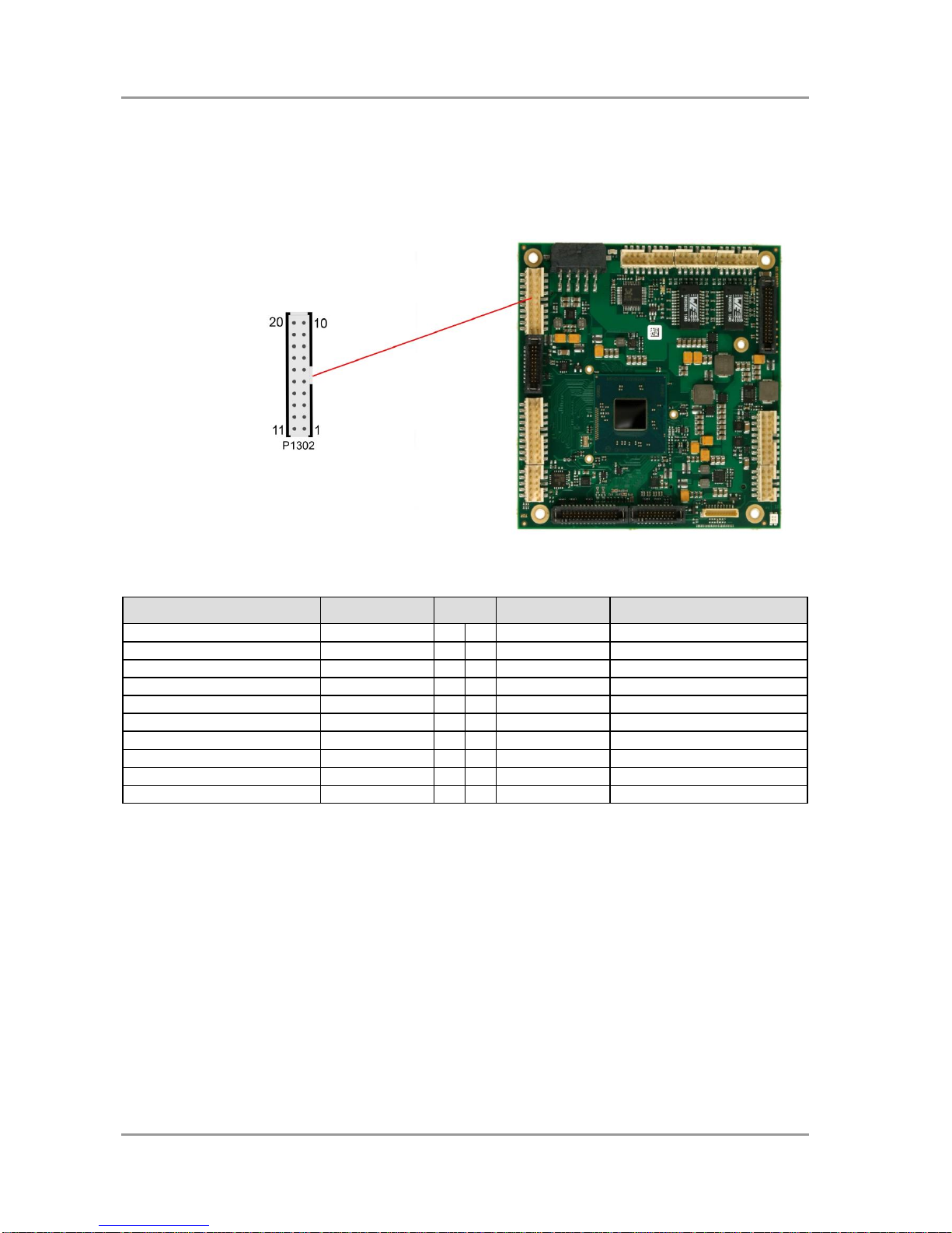
System/SM-Bus Chapter: Connectors
ADL Embedded Solutions ADLE3800PC page 15
3.3 System/SM-Bus
Both SM-Bus signals, and signals e.g. speaker are provided through a 2x10pin connector (FCI
98424-G52-20LF, mating connector e.g. FCI 90311-020LF). For the #PSON signal, please refer to the
cautionary note in the chapter "Power Supply" (page 14).
Pinout 2x10 system connector:
Dsecription
Name
Pin
Name
Description
ATX Powerbutton
ATXPWRBTN#
1
11
GND
ground
reset to ground
RSTBTN#
2
12
GND
ground
battery
BATT
3
13
GND
ground
speaker
SPEAKER
4
14
VCC
5V supply
SATA LED
SATALED#
5
15
3.3V
3.3V supply
Rot / LED0
RED/LED 0
6
16
GREEN/LED1
green / LED1
Blau / LED2
BLUE/LED2
7
17
S3.3V
standby supply 3.3V
PS-ON
PSON#
8
18
S3.3V
standby supply 3.3V
Systembus clock
SMB-CLK
9
19
SMB-ALERT
Systembus alert
Systembus data
SMB-DAT
10
20
GND
ground
Page 16
Chapter: Connectors Memory
page 16 ADL Embedded Solutions ADLE3800PC
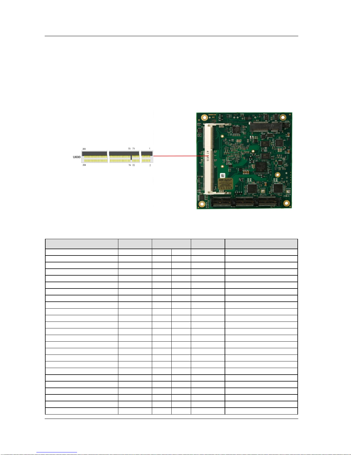
3.4 Memory
There is one conventional SO-DIMM204 socket available to equip the board with memory (DDR3L-1333).
It is located on the bottom side of the board. For technical and mechanical reasons it is possible that
particular memory modules cannot be employed. Please ask your sales representative for recommended
memory modules.
With currently available SO-DIMM modules a memory extension up to 8 GByte is possible. The timing
parameters for different memory modules are automatically set by BIOS.
Pinout SO-DIMM204:
Description
Name
Pin
Name
Description
memory reference current
REF-DQ
1 2 GND
ground
ground
GND
3 4 DQ4
data 4
data 0
DQ0
5 6 DQ5
data 5
data 1
DQ1
7 8 GND
ground
ground
GND
9
10
DQS0#
data strobe 0 -
data mask 0
DM0
11
12
DQS0
data strobe 0 +
ground
GND
13
14
GND
ground
data 2
DQ2
15
16
DQ6
data 6
data 3
DQ3
17
18
DQ7
data 7
ground
GND
19
20
GND
ground
data 8
DQ8
21
22
DQ12
data 12
data 9
DQ9
23
24
DQ13
data 13
ground
GND
25
26
GND
ground
data strobe 1 -
DQS1#
27
28
DM1
data mask 1
data strobe 1 +
DQS1
29
30
RESET#
Reset
ground
GND
31
32
GND
ground
data 10
DQ10
33
34
DQ14
data 14
data 11
DQ11
35
36
DQ15
data 15
ground
GND
37
38
GND
ground
data 16
DQ16
39
40
DQ20
data 20
data 17
DQ17
41
42
DQ21
data 21
ground
GND
43
44
GND
ground
data strobe 2 -
DQS2#
45
46
DM2
data mask 2
data strobe 2 +
DQS2
47
48
GND
ground
ground
GND
49
50
DQ22
data 22
Page 17

Memory Chapter: Connectors
ADL Embedded Solutions ADLE3800PC page 17
Description
Name
Pin
Name
Description
data 18
DQ18
51
52
DQ23
data 23
data 19
DQ19
53
54
GND
ground
ground
GND
55
56
DQ28
data 28
data 24
DQ24
57
58
DQ29
data 29
data 25
DQ25
59
60
GND
ground
ground
GND
61
62
DQS3#
data strobe 3 -
data mask 3
DQM3
63
64
DQS3
data strobe 3 +
ground
GND
65
66
GND
ground
data 26
DQ26
67
68
DQ30
data 30
data 27
DQ27
69
70
DQ31
data 31
ground
GND
71
72
GND
ground
clock enables 0
CKE0
73
74
CKE1
clock enables 1
1.5 volt supply
1.5V
75
76
1.5V
1.5 volt supply
reserved
N/C
77
78
(A15)
reserved
SDRAM bank 2
BA2
79
80
A14
address 14
1.5 volt supply
1.5V
81
82
1.5V
1.5 volt supply
address 12 (burst chop)
A12/BC#
83
84
A11
address 11
address 9
A9
85
86
A7
address 7
1.5 volt supply
1.5V
87
88
1.5V
1.5 volt supply
address 8
A8
89
90
A6
address 6
address 5
A5
91
92
A4
address 4
1.5 volt supply
1.5V
93
94
1.5V
1.5 volt supply
address 3
A3
95
96
A2
address 2
address 1
A1
97
98
A0
address 0
1.5 volt supply
1.5V
99
100
1.5V
1.5 volt supply
Clock 0 +
CK0
101
102
CK1
clock 1 +
Clock 0 -
CK0#
103
104
CK1#
clock 1 -
1.5 volt supply
1.5V
105
106
1.5V
1.5 volt supply
address 10 (auto precharge)
A10/AP
107
108
BA1
SDRAM bank 1
SDRAM Bank 0
BA0
109
110
RAS#
row address strobe
1.5 volt supply
1.5V
111
112
1.5V
1.5 volt supply
write enable
WE#
113
114
S0#
chip select 0
column address strobe
CAS#
115
116
ODT0
on die termination 0
1.5 volt supply
1.5V
117
118
1.5V
1.5 volt supply
address 13
A13
119
120
ODT1
on die termination 1
Chip Select 1
S1#
121
122
N/C
reserved
1.5 volt supply
1.5V
123
124
1.5V
1.5 volt supply
reserved
(TEST)
125
126
REF-CA
reference current
ground
GND
127
128
GND
ground
data 32
DQ32
129
130
DQ36
data 36
data 33
DQ33
131
132
DQ37
data 37
ground
GND
133
134
GND
ground
data strobe 4 -
DQS4#
135
136
DQM4
data mask 4
data strobe 4 +
DQS4
137
138
GND
ground
ground
GND
139
140
DQ38
data 38
data 34
DQ34
141
142
DQ39
data 39
data 35
DQ35
143
144
GND
ground
ground
GND
145
146
DQ44
data 44
data 40
DQ40
147
148
DQ45
data 45
data 41
DQ41
149
150
GND
ground
ground
GND
151
152
DQS5#
data strobe 5 -
data mask 5
DQM5
153
154
DQS5
data strobe 5 +
ground
GND
155
156
GND
ground
data 42
DQ42
157
158
DQ46
data 46
data 43
DQ43
159
160
DQ47
data 47
Page 18

Chapter: Connectors Memory
page 18 ADL Embedded Solutions ADLE3800PC
Description
Name
Pin
Name
Description
ground
GND
161
162
GND
ground
data 48
DQ48
163
164
DQ52
data 52
data 49
DQ49
165
166
DQ53
data 53
ground
GND
167
168
GND
ground
data strobe 6 -
DQS6#
169
170
DQM6
data mask 6
data strobe 6
DQS6
171
172
GND
ground
ground
GND
173
174
DQ54
data 54
data 50
DQ50
175
176
DQ55
data 55
data 51
DQ51
177
178
GND
ground
ground
GND
179
180
DQ60
data 60
data 56
DQ56
181
182
DQ61
data 61
data 57
DQ57
183
184
GND
ground
ground
GND
185
186
DQS7#
data strobe 7 -
data mask 7
DQM7
187
188
DQS7
data strobe 7 +
ground
GND
189
190
GND
ground
data 58
DQ58
191
192
DQ62
data 62
data 59
DQ59
193
194
DQ63
data 63
ground
GND
195
196
GND
ground
SPD address 0
SA0
197
198
EVENT#
Event
3.3 volt supply
3.3V
199
200
SDA
SMBus data
SPD address 1
SA1
201
202
SCL
SMBus clock
termination current
VTT
203
204
VTT
termination current
Page 19

PCI/104-Express Bus Chapter: Connectors
ADL Embedded Solutions ADLE3800PC page 19
3.5 PCI/104-Express Bus
Expansion modules for the PCI-Express bus can be connected to the board using the PCI/104-Express™
connector. This is a "type 2" connector with only those signals connected that are supported by the
chipset. "Stacking Error" functionality is available. For specifics, please refer to the PCI/104-Express™
documentation (rev. 2.01).
Pinout PCI104-Express connector (type 2):
Description
Name
Pin
Name
Description
USB Overcurrent
USBOC#
1 2 PERST#
PCIe reset
3.3V supply
3.3V
3 4 3.3V
3.3V supply
USB7 +
USB7
5 6 USB8
USB8 +
USB7 -
USB7#
7 8 USB8#
USB8 -
ground
GND
9
10
GND
ground
transmit lane 2 +
PEx1_1T
11
12
PEx1_0T
transmit lane 1 +
transmit lane 2 -
PEx1_1T#
13
14
PEx1_0T#
transmit lane 1 -
ground
GND
15
16
GND
ground
reserved
N/C
17
18
N/C
reserved
reserved
N/C
19
20
N/C
reserved
ground
GND
21
22
GND
ground
receive lane 2 +
PEx1_1R
23
24
PEx1_0R
receive lane 1 +
receive lane 2 -
PEx1_1R#
25
26
PEx1_0R#
receive lane 1 -
ground
GND
27
28
GND
ground
reserved
N/C
29
30
N/C
reserved
reserved
N/C
31
32
N/C
reserved
ground
GND
33
34
GND
ground
clock slot 2 +
PEx1_1C
35
36
PEx1_0C
clock slot 1 +
clock slot 2 -
PEx1_1C#
37
38
PEx1_0C#
clock slot 1 -
5V standby supply
SVCC
39
40
SVCC
5V standby supply
reserved
N/C
41
42
N/C
reserved
reserved
N/C
43
44
N/C
reserved
CPU direction
CPU_DIR
45
46
PWRGOOD
Powergood
SMBus data
SMBDAT
47
48
N/C
reserved
SMBus clock
SMBCLK
49
50
N/C
reserved
SMBus alert
SMBALERT
51
52
PSON#
PS ON
link reactivation
PEWAKE#
53
54
ST1-ERR#
stacking error 1
Page 20

Chapter: Connectors PCI/104-Express Bus
page 20 ADL Embedded Solutions ADLE3800PC
Description
Name
Pin
Name
Description
ground
GND
55
56
GND
ground
reserved
N/C
57
58
N/C
reserved
reserved
N/C
59
60
N/C
reserved
ground
GND
61
62
GND
ground
reserved
N/C
63
64
N/C
reserved
reserved
N/C
65
66
N/C
reserved
ground
GND
67
68
GND
ground
reserved
N/C
69
70
N/C
reserved
reserved
N/C
71
72
N/C
reserved
ground
GND
73
74
GND
ground
reserved
N/C
75
76
N/C
reserved
reserved
N/C
77
78
N/C
reserved
ground
GND
79
80
GND
ground
reserved
N/C
81
82
N/C
reserved
reserved
N/C
83
84
N/C
reserved
ground
GND
85
86
GND
ground
reserved
N/C
87
88
N/C
reserved
reserved
N/C
89
90
N/C
reserved
ground
GND
91
92
GND
ground
reserved
N/C
93
94
N/C
reserved
reserved
N/C
95
96
N/C
reserved
ground
GND
97
98
GND
ground
reserved
N/C
99
100
N/C
reserved
reserved
N/C
101
102
N/C
reserved
ground
GND
103
104
GND
ground
stacking error 2
ST2-ERR#
105
106
LPCCLK
PCI clock
ground
GND
107
108
GND
ground
reserved
N/C
109
110
N/C
reserved
reserved
N/C
111
112
N/C
reserved
ground
GND
113
114
GND
ground
reserved
N/C
115
116
N/C
reserved
reserved
N/C
117
118
N/C
reserved
ground
GND
119
120
GND
ground
reserved
N/C
121
122
N/C
reserved
reserved
N/C
123
124
N/C
reserved
ground
GND
125
126
GND
ground
reserved
N/C
127
128
N/C
reserved
reserved
N/C
129
130
N/C
reserved
ground
GND
131
132
GND
ground
reserved
N/C
133
134
N/C
reserved
reserved
N/C
135
136
N/C
reserved
ground
GND
137
138
GND
ground
reserved
N/C
139
140
N/C
reserved
reserved
N/C
141
142
N/C
reserved
ground
GND
143
144
GND
ground
LPC address/data 0
LPCAD0
145
146
LPCDRQ#
LPC DMA request
LPC address/data 1
LPCAD1
147
148
LPCSIRQ#
LPC serial IRQ
ground
GND
149
150
GND
ground
LPC address/data 2
LPCAD2
151
152
LPCFRAME#
LPC frame
LPC address/data 3
LPCAD3
153
154
RTCBATT
battery 3.3V
ground
GND
155
156
GND
ground
5V supply
VCC
C1
5V supply
VCC
C2
12V supply
12V
C3
Page 21
PCI-Express Mini Card with mSATA Chapter: Connectors
ADL Embedded Solutions ADLE3800PC page 21
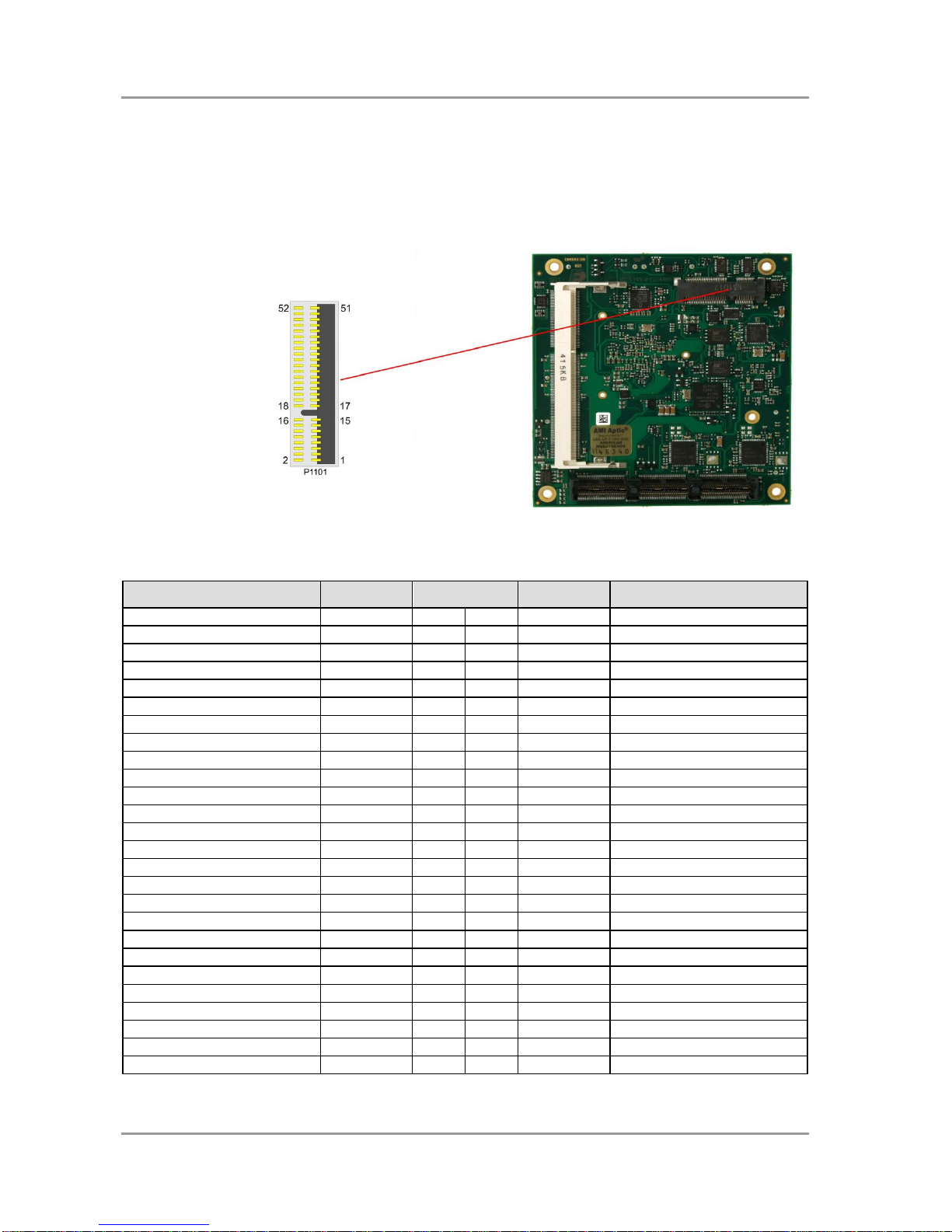
3.6 PCI-Express Mini Card with mSATA
As a soldering option, the ADLE3800PC can be equipped with PCI-Express Mini Card connector to
interface with approved peripherals, such as Wi-FI and storage cards via miniPCIe. In addition the PCIe
Mini Card connector supports storage modules via mSATA.
Description
Name
Pin
Name
Description
PCIe Wake
PEWAKE#
1 2 S3.3V
3.3V standby supply
reserved
N/C 3 4
MPCIeEN
configuration mPCIe#
reserved
N/C 5 6
1.5V
1.5V supply
clock enable
PEMCLKen#
7 8 N/C
reserved
ground
GND
9
10
N/C
reserved
clock -
PECLKMC#
11
12
N/C
reserved
clock +
PECLKMC
13
14
N/C
reserved
ground
GND
15
16
N/C
reserved
reserved
N/C
17
18
GND
ground
reserved
N/C
19
20
WDISABLE#
wireless disable
ground
GND
21
22
PERST#
PCIe reset
PCIe receive -
PERMC#
23
24
S3.3V
3.3V standby supply
PCIe receive +
PERMC
25
26
GND
ground
ground
GND
27
28
1.5V
1.5V supply
ground
GND
29
30
SMB-CLK
SM-Bus clock
PCIe transmit -
PETMC#
31
32
SMB-DAT
SM-Bus data
PCIe transmit +
PETMC
33
34
GND
ground
ground
GND
35
36
USBMC#
USB -
ground
GND
37
38
USBMC
USB +
3.3V supply
S3.3V
39
40
GND
ground
3.3V supply
S3.3V
41
42
N/C
reserved
ground
GND
43
44
N/C
reserved
reserved
N/C
45
46
N/C
reserved
reserved
N/C
47
48
1.5V
1.5V supply
reserved
N/C
49
50
GND
ground
configuration MSATA
MSATA#
51
52
S3.3V
3.3V standby supply
Page 22
Chapter: Connectors DVI/HDMI/VGA
page 22 ADL Embedded Solutions ADLE3800PC
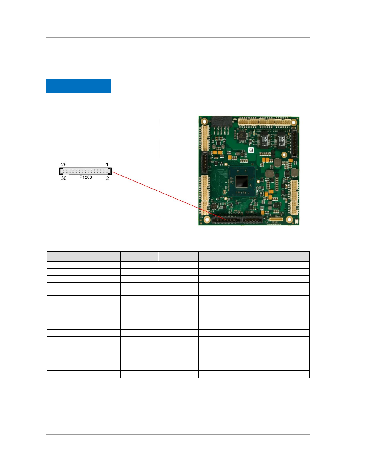
3.7 DVI/HDMI/VGA
The ADLE3800PC provides a DVI/HDMI/VGA interface which is realized as a 2x15pin header
(TFM-115-02-S-D-WT, mating connector e.g. SFM-115-02-S-D-xx).
For parallel use of DVI- and CRT signals a custom cable design will be
required. Please ask your distributor for recommended products.
Pinout 2x15 connector DVI/HDMI/VGA:
Description
Name
Pin
Name
Description
Red
Red 1 2
GND
ground
Green
Green
3
4
CS-DDDA
DDC data
Blue
Blue
5
6
CS-DDCK
DDC clock
CS-VSYNC (Vertical
synchronization)
CS-VSYNC
7
8
GND
ground
CS-HSYNC (Horizontal
synchronization)
CS-HSYNC
9
10
GND
ground
5 volt supply
VCC
11
12
GND
ground
Hot Plug Detect
HPD
13
14
N/A
reserved
DDC clock
DDCCLK
15
16
DDCDAT
DDC data +
5 volt supply
VCC
17
18
GND
ground
ground
GND
19
20
TMDSCLK#
TMDS clock -
TMDS data -
TMDS#0
21
22
TMDSCLK
TMDS clock
TMDS data +
TMDS0
23
24
GND
ground
ground
GND
25
26
TMDS#1
TMDS data -
TMDS data -
TMDS#2
27
28
TMDS1
TMDS data +
TMDS data +
TMDS2
29
30
GND
ground
NOTICE
Page 23
DisplayPort Chapter: Connectors
ADL Embedded Solutions ADLE3800PC page 23
3.8 DisplayPort
The ADLE3800PC offers a DisplayPort interface which is realized as 2x10pin connector
(TFM-110-02-S-D-WT, mating connector SFM-110-02-S-D-xx). This interface can also be operated in
HDMI/DVI mode. To achieve this, pin 2 must be connected to 3.3V (e.g. pin 5).
Pinout 2x10pin DisplayPort connector:
Description
Name
Pin
Name
Description
Hotplug detect
DPHPD
1 2 HDMIEN
HDMI enable
DP Aux + / EDID Clock
DPAUX/DDC
K
3 4 DPAUX#/DD
DA
DP Aux - / EDID data
3.3V supply
3.3V
5 6 GND
Ground
Ground
GND
7 8 DPL3#/TMD
SCLK#
DP Lane 3 - / HDMI Clock -
DP Lane 2 - / HDMI 0 -
DPL2#/TMD
S0#
9
10
DPL3/TMDS
CLK
DP Lane 3 + / HDMI Clock +
DP Lane 2 + / HDMI 0 +
DPL2/TMDS
0
11
12
GND
Ground
Ground
GND
13
14
DPL1#/TMD
S1#
DP Lane 1 - / HDMI 1 -
DP Lane 0 - / HDMI 2 -
DPL0#/TMD
S2#
15
16
DPL1/TMDS
1
DP Lane 1 + / HDMI 1 +
DP Lane 0 + / HDMI 2 +
DPL0/TMDS
2
17
18
GND
Ground
Reserved
N/C
19
20
GND
Ground
Page 24
Chapter: Connectors USB 2.0
page 24 ADL Embedded Solutions ADLE3800PC
3.9 USB 2.0
USB channels 2, 3, 5 and 6 are provided via two 2x8pin connectors (FCI 98424-G52-16LF, mating
connector e.g. FCI 90311-016LF).
All USB-channels support USB 2.0. You may note that the setting of USB keyboard or USB mouse
support in the BIOS-setup is only necessary and advisable, if the OS offers no USB-support. BIOS-setup
can be changed with a USB keyboard without enabling USB keyboard support. Running a USB
supporting OS (such as Microsoft® Windows®) with these features enabled may lead to significant
performance or functionality limitations.
Every USB interface provides up to 500 mA current and is protected by an electronically resettable fuse.
Pinout USB 2, 3, 5 and 6:
Description
Name
Pin
Name
Description
5V for USB2
USB2 VCC
1 9 USB3VCC
5V for USB3
USB- data lane 2
USB2#
2
10
USB3#
USB- data lane 3
USB+ data lane 2
USB2
3
11
USB3
USB+ data lane 3
ground
GND
4
12
GND
ground
ground
GND
5
13
GND
ground
USB+ data lane 5
USB5
6
14
USB6
USB+ data lane 6
USB- data lane 5
USB5#
7
15
USB6#
USB- data lane 6
5V for USB5
USB5VCC
8
16
USB6VCC
5V for USB6
Page 25

USB 3.0 Chapter: Connectors
ADL Embedded Solutions ADLE3800PC page 25
3.10 USB 3.0
USB channel 1 is provided via a two 2x10 pin connector (TFM-110-02-S-D-WT, mating connector e.g.
SFM-110-02-S-D-xx).
The USB-channel supports USB 3.0. You may note that the setting of USB keyboard or USB mouse
support in the BIOS-setup is only necessary and advisable, if the OS offers no USB-support. BIOS-setup
can be changed with a USB keyboard without enabling USB keyboard support. Running a USB
supporting OS (such as Microsoft® Windows®) with these features enabled may lead to significant
performance or functionality limitations.
Every USB interface provides up to 900 mA current and is protected by an electronically resettable fuse.
Pinout USB3.0 connector for port X:
Description
Name
Pin
Name
Description
reserved
N/C 1 2
N/C
reserved
USB x data +
USB3-x.D+
3 4 N/C
reserved
USB x data -
USB3-x.D-
5 6 GND
ground
ground
GND
7 8 N/C
reserved
USB x transmit +
SSTXx+
9
10
N/C
reserved
USB x transmit -
SSTXx-
11
12
GND
ground
ground
GND
13
14
N/C
reserved
USB x receive +
SSRX+
15
16
N/C
reserved
USB x receive -
SSRX-
17
18
N/C
reserved
power supply
VCC
19
20
N/C
reserved
Page 26
Chapter: Connectors LAN
page 26 ADL Embedded Solutions ADLE3800PC
3.11 LAN
Both LAN interfaces are provided via a 2x6pin connector (FCI 98424-G52-12LF, mating connector e.g.
FCI 90311-012LF). The interfaces support 10BaseT, 100BaseT, and 1000BaseT compatible network
components with automatic bandwidth selection. Additional outputs are provided for status LEDs.
Auto-negotiate and auto-cross functionality is available, PXE and RPL are available on request.
Pinout LAN interface:
Description
Name
Pin
Name
Description
LAN activity
LINKACT
1 7 SPEED1000
LAN speed 1000Mbit
LAN channel 1 plus
LAN1
2 8 LAN0
LAN channel 0 plus
LAN channel 1 minus
LAN1#
3 9 LAN0#
LAN channel 0 minus
LAN channel 3 plus
LAN3
4
10
LAN2
LAN channel 2 plus
LAN channel 3 minus
LAN3#
5
11
LAN2#
LAN channel 2 minus
LAN speed 100Mbit
SPEED100
6
12
3.3V
3.3 volt supply
Page 27

Audio Chapter: Connectors
ADL Embedded Solutions ADLE3800PC page 27
3.12 Audio
The ADLE3800PC's audio functions are provided via a 2x8pin connector (FCI 98424-G52-16LF, mating
connector e.g. FCI 90311-016LF). This interface provides eight output channels for full 7.1 sound output.
Two microphone inputs and two AUX inputs are also available.
The signals "SPDIFI" and "SPDIFO" provide digital input and output. If a transformation to a coaxial or
optical connector is necessary this must be performed externally.
Pinout Audio:
Description
Name
Pin
Name
Description
digital output SPDIF
SPDIFO
1 9 3.3V
3.3 volt supply
digital input SPDIF
SPDIFI
2
10
S_AGND
analog ground sound
sound output right
LOUT_R
3
11
LOUT_L
sound output left
AUX input right
AUXA_R
4
12
AUXA_L
AUX input left
microphone input 1
MIC1
5
13
MIC2
microphone input 2
surround out right
SOUT_R
6
14
SOUT_L
surround out left
center output
CENOUT
7
15
LFEOUT
LFE output
side surround out right
SSOUT_R
8
16
SSOUT_L
side surround out left
Page 28

Chapter: Connectors SATA Interfaces
page 28 ADL Embedded Solutions ADLE3800PC
3.13 SATA Interfaces
The ADLE3800PC provides two SATA interfaces allowing transfer rates of up to 3 Gbit per second.
These interfaces are made available via two 7 pin connectors.
The required settings are made in the BIOS setup.
Pinout SATA 2x15:
Description
Name
Pin
Pin
Name
Description
ground
GND
1 2 GND
ground
SATA1 transmit +
SATA1TX
3 4 SATA2TX
SATA2 transmit +
SATA1 transmit -
SATA1TX#
5 6 SATA2TX#
SATA2 transmit -
ground
GND
7 8 GND
ground
SATA1 receive -
SATA1RX#
9
10
SATA2RX#
SATA2 receive -
SATA1 transmit +
SATA1RX
11
12
SATA2RX
SATA2 receive +
ground
GND
13
14
GND
ground
reserved
N/C
15
16
N/C
reserved
ground
GND
17
18
GND
ground
reserved
N/C
19
20
N/C
reserved
reserved
N/C
21
22
N/C
reserved
ground
GND
23
24
GND
ground
reserved
N/C
25
26
N/C
reserved
reserved
N/C
27
28
N/C
reserved
ground
GND
29
30
GND
ground
Page 29

COM1 and COM2 Chapter: Connectors
ADL Embedded Solutions ADLE3800PC page 29
3.14 COM1 and COM2
The serial interfaces COM1 and COM2 are provided via a 2x5pin connector (FCI 98424-G52-10LF,
mating connector e.g. FCI 90311-010LF).
Description
Name
Pin
Name
Description
reserved
N/C 1 6
N/C
reserved
receive data
RXD
2 7 RTS
request to send
transmit data
TXD
3 8 CTS
clear to send
reserved
N/C 4 9
N/C
reserved
ground
GND
5
10
SVCC
5V standby supply
Page 30

Chapter: Connectors GPIO
page 30 ADL Embedded Solutions ADLE3800PC
3.15 GPIO
The General Purpose Input/Output interface is made available through a 2x10 pin connector (FCI
98424-G52-20LF, mating connector e.g. FCI 90311-020LF). To make use of this interface the SIO unit
must be programmed accordingly. Please refer to your sales representative for information on available
software support.
Pinout GPIO connector:
Description
Name
Pin
Name
Description
ground
GND
1
11
3.3V
3.3V supply
GP Input/Output A00
GPIOA.0
2
12
GPIOB.0
GP Input/Output B00
GP Input/Output A01
GPIOA.1
3
13
GPIOB.1
GP Input/Output B01
GP Input/Output A02
GPIOA.2
4
14
GPIOB.2
GP Input/Output B02
GP Input/Output A03
GPIOA.3
5
15
GPIOB.3
GP Input/Output B03
GP Input/Output A04
GPIOA.4
6
16
GPIOB.4
GP Input/Output B04
GP Input/Output A05
GPIOA.5
7
17
GPIOB.5
GP Input/Output B05
GP Input/Output A06
GPIOA.6
8
18
GPIOB.6
GP Input/Output B06
GP Input/Output A07
GPIOA.7
9
19
GPIOB.7
GP Input/Output B07
3.3V supply
3.3V
10
20
GND
ground
Page 31

Monitoring Functions Chapter: Connectors
ADL Embedded Solutions ADLE3800PC page 31
3.16 Monitoring Functions
Additional monitoring functions, such as the status of the fan or of other devices connected over SM-Bus
(e. g. temperature sensor), are accessible via an 10 pin connector (JST BM10B-SRSS-TB, mating
connector: SHR-10V-S(-B)).
Pin
Name
Description
1
3.3V
3.3V supply
2
CS-SMB-CLK
SMBus clock
3
CS-SMB-DAT
SMBus data
4
GND
ground
5
VCC
5V supply
6
FANPWM
FAN control
7
TACH
FAN monitoring
8
N/C
reserved
9
N/C
reserved
10
N/C
reserved
Page 32

Chapter: State LEDs HD LED
page 32 ADL Embedded Solutions ADLE3800PC
4 State LEDs
4.1 HD LED
Harddisk activity is signalled by a dedicated LED.
Page 33
RGB LED Chapter: State LEDs
ADL Embedded Solutions ADLE3800PC page 33
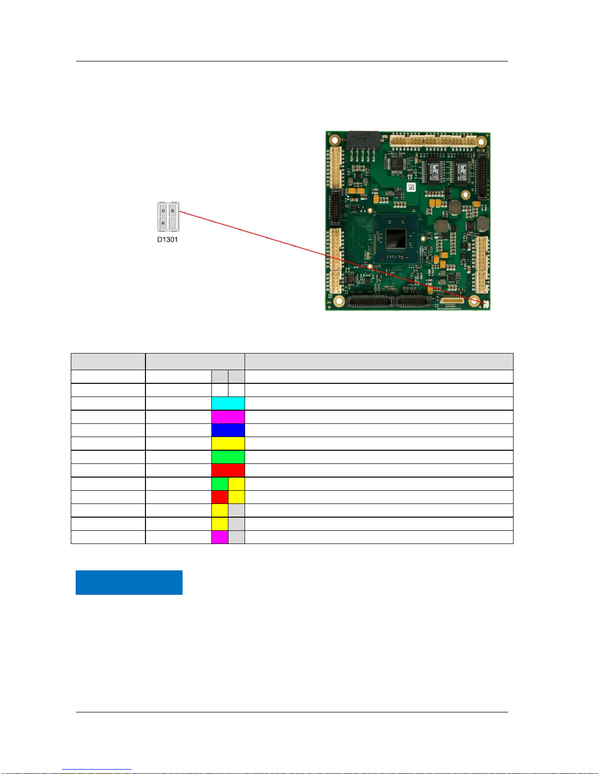
4.2 RGB LED
The ADLE3800PC has a tricolor LED, which signals status messages by using different colors and flash
intervals.
Status Codes RGB LED:
Color
Interval
Meaning
non
solid
Invalid system state
White
once
Powerfail
Cyan
solid
Reserved
Magenta
solid
if present: SUPS active
Blue
solid
Reserved
Yellow
solid
S5 state
Green
solid
S0 state
Red
solid
Reset/Start
Green/Yellow
flashing
Bootloader operates normal
Red/Yellow
flashing
Bootloader is being started (starting sequence still running)
Yellow
flashing (6s)
S4 state
Yellow
flashing (3s)
S3 state
Magenta
flashing (0,5s)
if present: SUPS test of capacity
If the board appears to be in Reset (Red LED lit) then this could also
indicate a PCI104-Express "stacking error". Such an error could occur
when the stack contains a peripheral card which has the wrong type of
connector (PCI104-Express Type 1 instead of Type 2 or vice versa).
NOTICE
Page 34
Chapter: State LEDs LAN Activity LED
page 34 ADL Embedded Solutions ADLE3800PC
4.3 LAN Activity LED
The ADLE3800PC has two unicolor LEDs, which signal LAN activity of the current LAN port.
LAN link activity:
Color
Interval
Meaning
none
solid
no LAN activity
green
flashing
LAN active
Page 35
LAN Speed LED Chapter: State LEDs
ADL Embedded Solutions ADLE3800PC page 35
4.4 LAN Speed LED
Two bicolor LEDs show the links speed of the current LAN port.
LAN speed:
Color
Interval
Meaning
none
solid
10 Mbit/s
orange
solid
100 Mbit/s
green
solid
1000 Mbit/s
Page 36

Chapter: BIOS Settings General Remarks
page 36 ADL Embedded Solutions ADLE3800PC
5 BIOS Settings
5.1 General Remarks
In each setup page, standard values for all setup entries can be loaded. Previously saved settings are
loaded by pressing F2 and factory defaults are loaded with F3. Both F2 and F3, and also F4 ("Save &
Exit") always affect the whole set of setup entries.
Setup entries starting with a „►" sign represent submenus. Navigation between entries is done using the
arrow keys on the keyboard, with the <Enter> key being used to select an entry, which either opens up a
dialog box or opens a whole new submenu of setup entries.
Each setup entry has a short help text associated with it. This is displayed in the upper right hand corner
of the screen.
Page 37

Main Chapter: BIOS Settings
ADL Embedded Solutions ADLE3800PC page 37
5.2 Main
Aptio Setup Utility - Copyright (C) 2016 American Megatrends, Inc.
MAIN Advanced Chipset Security Boot Save & Exit
┌─────────────────────────────────────────────────────────────────┬────────────────────────────────┐
│ │Set the Date. Use Tab to │
│ Board Information │switch between Data elements. │
│ Board ADLE3800PC │ │
│ Revision f │ │
│ Bios Version 0.08 │ │
│ │ │
│ CPU Configuration │ │
│ Microcode Patch 321 │ │
│ BayTrail SoC B2 Stepping │ │
│ │ │
│ Memory Information │ │
│ Total Memory 8192 MB (LPDDR3) │ │
│ │────────────────────────────────│
│ System Date [Sun 12/05/2014] │→←: Select Screen │
│ System Time [00:47:04] │↑↓: Select Item │
│ │Enter: Select │
│ │+/-: Change Opt. │
│ │F1: General Help │
│ │F2: Previous Values │
│ │F3: Optimized Defaults │
│ │F4: Save & Exit │
│ │ESC: Exit │
│ │ │
│ │ │
│ │ │
│ │ │
└─────────────────────────────────────────────────────────────────┴────────────────────────────────┘
Version 2.17.1249. Copyright (C) 2016 American Megatrends, Inc.
Board
Options: none
Revision
Options: none
Bios Version
Options: none
Microcode Patch
Options: none
BayTrail SoC
Options: none
Total Memory
Options: none
System Date
Options: The system date can be adjusted here.
System Time
Options: The system time can be adjusted here.
Page 38

Chapter: BIOS Settings Advanced
page 38 ADL Embedded Solutions ADLE3800PC
5.3 Advanced
Aptio Setup Utility - Copyright (C) 2013 American Megatrends, Inc.
Main ADVANCED Chipset Security Boot Save & Exit
┌─────────────────────────────────────────────────────────────────┬────────────────────────────────┐
│ Power-Supply Type [ATX] │Select the Type of the Power │
│► ACPI Settings │Supply: AT/ATX │
│► Hardware Monitor │ │
│► CPU Configuration │ │
│► PPM Configuration │ │
│► SATA Configuration │ │
│► Miscellaneous Configuration │ │
│► LPSS & SCC Configuration │ │
│► Network Stack Configuration │ │
│► Power Controller Options │ │
│► CSM Configuration │ │
│► SDIO Configuration │ │
│► USB Configuration │────────────────────────────────│
│► Security Configuration │→←: Select Screen │
│ │↑↓: Select Item │
│ │Enter: Select │
│ │+/-: Change Opt. │
│ │F1: General Help │
│ │F2: Previous Values │
│ │F3: Optimized Defaults │
│ │F4: Save & Exit │
│ │ESC: Exit │
│ │ │
│ │ │
│ │ │
│ │ │
└─────────────────────────────────────────────────────────────────┴────────────────────────────────┘
Version 2.16.1242. Copyright (C) 2013 American Megatrends, Inc.
PCI RT32 Service
Options: Enabled / Disabled
ACPI Settings
Sub menu: see "ACPI Settings" (page 40)
H/W Monitor
Sub menu: see "H/W Monitor" (page 41)
CPU Configuration
Sub menu: see "CPU Configuration" (page 43)
PPM Configuration
Sub menu: see "PPM Configuration" (page 47)
SATA Configuration
Sub menu: see "SATA Configuration" (page 48)
Miscellaneous Configuration
Sub menu: see "Miscellaneous Configuration" (page 49)
LPSS & SCC Configuration
Sub menu: see "LPSS & SCC Configuration" (page 50)
Network Stack Configuration
Sub menu: see "Network Stack" (page 52)
Power Controller Options
Sub menu: see "Power Controller Options" (page 53)
CSM Configuration
Sub menu: see "CSM Configuration" (page 55)
Page 39

Advanced Chapter: BIOS Settings
ADL Embedded Solutions ADLE3800PC page 39
SDIO Configuration
Sub menu: see "SDIO Configuration" (page 56)
USB Configuration
Sub menu: see "USB Configuration" (page 57)
Security Configuration
Sub menu: see "Security Configuration" (page 58)
Page 40

Chapter: BIOS Settings Advanced
page 40 ADL Embedded Solutions ADLE3800PC
5.3.1 ACPI Settings
Aptio Setup Utility - Copyright (C) 2016 American Megatrends, Inc.
Advanced
┌─────────────────────────────────────────────────────────────────┬────────────────────────────────┐
│ ACPI Settings │Enables or Disables BIOS ACPI │
│ │Auto Configuration. │
│ Enable ACPI Auto Configuration [Disabled] │ │
│ │ │
│ Enable Hibernation [Enabled] │ │
│ ACPI Sleep State [Suspend Disabled] │ │
│ Lock Legacy Resources [Disabled] │ │
│ │ │
│ │ │
│ │ │
│ │ │
│ │ │
│ │────────────────────────────────│
│ │→←: Select Screen │
│ │↑↓: Select Item │
│ │Enter: Select │
│ │+/-: Change Opt. │
│ │F1: General Help │
│ │F2: Previous Values │
│ │F3: Optimized Defaults │
│ │F4: Save & Exit │
│ │ESC: Exit │
│ │ │
│ │ │
│ │ │
│ │ │
└─────────────────────────────────────────────────────────────────┴────────────────────────────────┘
Version 2.17.1249. Copyright (C) 2016 American Megatrends, Inc.
Enable ACPI Auto Configuration
Options: Enabled / Disabled
Enable Hibernation
Options: Enabled / Disabled
ACPI Sleep State
Options: Suspend Disabled / S1 (CPU Stop Clock)
Lock Legacy Resources
Options: Enabled / Disabled
Page 41

Advanced Chapter: BIOS Settings
ADL Embedded Solutions ADLE3800PC page 41
5.3.2 H/W Monitor
Aptio Setup Utility - Copyright (C) 2013 American Megatrends, Inc.
Advanced
┌─────────────────────────────────────────────────────────────────┬────────────────────────────────┐
│ Pc Health Status │ │
│ │ │
│ CPU dig. : +44 'C │ │
│ 1.05V : +1.04 V │ │
│ VCCCORE : +0.71 V │ │
│ 5V : +5.05 V │ │
│ 12V : +12.18 V │ │
│ VBATT : +0.3 │ │
│ FAN 1 : N/A │ │
│ FAN 2 : N/A │ │
│ FAN 3 : N/A │ │
│ MB Temp : +44 'C │ │
│ Memory Temp : +44 'C │────────────────────────────────│
│ PwrCtrlTemp : +47 'C │→←: Select Screen │
│ PwrCtrlVCC : +7.70 V │↑↓: Select Item │
│ │Enter: Select │
│ │+/-: Change Opt. │
│ │F1: General Help │
│ │F2: Previous Values │
│ │F3: Optimized Defaults │
│ │F4: Save & Exit │
│ │ESC: Exit │
│ │ │
│ │ │
│ │ │
│ │ │
└─────────────────────────────────────────────────────────────────┴────────────────────────────────┘
Version 2.16.1242. Copyright (C) 2013 American Megatrends, Inc.
CPU dig.
Options: none
1.05V
Options: none
VCCCORE
Options: none
5V
Options: none
12V
Options: none
AUX FAN Speed
Options: none
VBATT
Options: none
FAN 1
Options: none
FAN 2
Options: none
FAN 3
Options: none
MB Temp
Options: none
Page 42

Chapter: BIOS Settings Advanced
page 42 ADL Embedded Solutions ADLE3800PC
Memory Temp
Options: none
PwrCtrlTemp
Options: none
PwrCtrlVCC
Options: none
Page 43

Advanced Chapter: BIOS Settings
ADL Embedded Solutions ADLE3800PC page 43
5.3.3 CPU Configuration
Aptio Setup Utility - Copyright (C) 2013 American Megatrends, Inc.
Advanced
┌─────────────────────────────────────────────────────────────────┬────────────────────────────────┐
│ CPU Configuration │Socket specific CPU Information │
│ │ │
│► Socket 0 CPU Information │ │
│► CPU Thermal Configuration │ │
│ │ │
│ CPU Speed 1467 MHz │ │
│ 64-bit Supported │ │
│ │ │
│ Active Processor Cores [All] │ │
│ Limit CPUID Maximum [Disabled] │ │
│ Execute Disable Bit [Enabled] │ │
│ Hardware Prefetcher [Enabled] │ │
│ Adjacent Cache Line Prefetch [Enabled] │ │
│ Intel Virtualization Technology [Enabled] │ │
│ Power Technology [Custom] │ │
│ EIST [Enabled] │────────────────────────────────│
│ P-STATE Coordination [HW_ALL] │→←: Select Screen │
│ CPU C6 report [Enabled] │↑↓: Select Item │
│ Package C State limit [No Limit] │Enter: Select │
│ │+/-: Change Opt. │
│ │F1: General Help │
│ │F2: Previous Values │
│ │F3: Optimized Defaults │
│ │F4: Save & Exit │
│ │ESC: Exit │
│ │ │
│ │ │
│ │ │
└─────────────────────────────────────────────────────────────────┴────────────────────────────────┘
Version 2.16.1242. Copyright (C) 2013 American Megatrends, Inc.
Socket 0 CPU Information
Sub menu: see "Socket CPU Information" (page 45)
CPU Thermal Configuration
Sub menu: see "CPU Thermal Configuration" (page 46)
CPU Speed
Options: none
64-bit
Options: none
Active Processor Cores
Options: All / One / Two / Three
Limit CPUID Maximum
Options: Enabled / Disabled
Execute Disable Bit
Options: Enabled / Disabled
Hardware Prefetcher
Options: Disabled / Enabled
Adjacent Cache Line Prefetch
Options: Disabled / Enabled
Intel Virtualization Technology
Options: Enabled / Disabled
Power Technology
Options: Disable / Energy Efficient / Custom
Page 44

Chapter: BIOS Settings Advanced
page 44 ADL Embedded Solutions ADLE3800PC
EIST
Options: Disabled / Enabled
P-STATE Coordination
Options: HW_ALL / SW_ALL / SW_ANY
C6 report
Options: Disabled / Enabled
Package C State limit
Options: C0 / C1 / C3 / C6 / C7 / No Limit
Page 45

Advanced Chapter: BIOS Settings
ADL Embedded Solutions ADLE3800PC page 45
5.3.3.1 Socket CPU Information
Aptio Setup Utility - Copyright (C) 2016 American Megatrends, Inc.
Advanced
┌─────────────────────────────────────────────────────────────────┬────────────────────────────────┐
│ Socket 0 CPU Information │ │
│ │ │
│ Intel(R) Atom(TM) CPU E3845 @ 1.91GHz │ │
│ CPU Signature 30679 │ │
│ Microcode Patch 901 │ │
│ Max CPU Speed 1910 MHz │ │
│ Min CPU Speed 500 MHz │ │
│ Processor Cores 4 │ │
│ Intel HT Technology Not Supported │ │
│ Intel VT-x Technology Supported │ │
│ │ │
│ L1 Data Cache 24 kB x 4 │ │
│ L1 Code Cache 32 x kB 4 │ │
│ L2 Cache 1024 kB x 2 │ │
│ L3 Cache Not Present │ │
│ │────────────────────────────────│
│ │→←: Select Screen │
│ │↑↓: Select Item │
│ │Enter: Select │
│ │+/-: Change Opt. │
│ │F1: General Help │
│ │F2: Previous Values │
│ │F3: Optimized Defaults │
│ │F4: Save & Exit │
│ │ESC: Exit │
│ │ │
│ │ │
│ │ │
└─────────────────────────────────────────────────────────────────┴────────────────────────────────┘
Version 2.17.1249. Copyright (C) 2016 American Megatrends, Inc.
CPU Signature
Options: none
Microcode Patch
Options: none
Max CPU Speed
Options: none
Min CPU Speed
Options: none
Processor Cores
Options: none
Intel HT Technology
Options: none
Intel VT-x Technology
Options: none
L1 Data Cache
Options: none
L1 Code Cache
Options: none
L2 Cache
Options: none
L3 Cache
Options: none
Page 46

Chapter: BIOS Settings Advanced
page 46 ADL Embedded Solutions ADLE3800PC
5.3.3.2 CPU Thermal Configuration
Aptio Setup Utility - Copyright (C) 2016 American Megatrends, Inc.
Advanced
┌─────────────────────────────────────────────────────────────────┬────────────────────────────────┐
│ CPU Thermal Configuration │Enabled/Disable Digital │
│ DTS [Disabled] │Thermal Sensor. │
│ │ │
│ │ │
│ │ │
│ │ │
│ │ │
│ │ │
│ │ │
│ │ │
│ │ │
│ │ │
│ │ │
│ │ │
│ │ │
│ │────────────────────────────────│
│ │→←: Select Screen │
│ │↑↓: Select Item │
│ │Enter: Select │
│ │+/-: Change Opt. │
│ │F1: General Help │
│ │F2: Previous Values │
│ │F3: Optimized Defaults │
│ │F4: Save & Exit │
│ │ESC: Exit │
│ │ │
│ │ │
│ │ │
└─────────────────────────────────────────────────────────────────┴────────────────────────────────┘
Version 2.17.1249. Copyright (C) 2016 American Megatrends, Inc.
DTS
Options: Enabled / Disabled
Page 47

Advanced Chapter: BIOS Settings
ADL Embedded Solutions ADLE3800PC page 47
5.3.4 PPM Configuration
Aptio Setup Utility - Copyright (C) 2013 American Megatrends, Inc.
Advanced
┌─────────────────────────────────────────────────────────────────┬────────────────────────────────┐
│ PPM Configuration │Enable/Disable Intel SpeedStep │
│ │ │
│ EIST [Enabled] │ │
│ CPU C state Report [Enabled] │ │
│ Enhanced C state [Enabled] │ │
│ Max CPU C-state [ C7] │ │
│ S0ix [Disabled] │ │
│ │ │
│ │ │
│ │ │
│ │ │
│ │ │
│ │ │
│ │ │
│ │ │
│ │────────────────────────────────│
│ │→←: Select Screen │
│ │↑↓: Select Item │
│ │Enter: Select │
│ │+/-: Change Opt. │
│ │F1: General Help │
│ │F2: Previous Values │
│ │F3: Optimized Defaults │
│ │F4: Save & Exit │
│ │ESC: Exit │
│ │ │
│ │ │
│ │ │
└─────────────────────────────────────────────────────────────────┴────────────────────────────────┘
Version 2.16.1242. Copyright (C) 2013 American Megatrends, Inc.
EIST
Options: Disabled / Enabled
CPU C state Report
Options: Disabled / Enabled
Enhanced C state
Options: Disabled / Enabled
Max CPU C-state
Options: C7 / C6 / C1
S0ix
Options: Disabled / Enabled
Page 48

Chapter: BIOS Settings Advanced
page 48 ADL Embedded Solutions ADLE3800PC
5.3.5 SATA Configuration
Aptio Setup Utility - Copyright (C) 2013 American Megatrends, Inc.
Advanced
┌─────────────────────────────────────────────────────────────────┬────────────────────────────────┐
│ SATA Configuration │Enable / Disable Serial ATA │
│ │ │
│ Serial-ATA (SATA) [Enabled] │ │
│ SATA Test Mode [Disabled] │ │
│ │ │
│ SATA Speed Support [Gen1] │ │
│ SATA ODD Port [No ODD] │ │
│ SATA Mode [AHCI Mode] │ │
│ │ │
│ Serial-ATA Port 0 [Enabled] │ │
│ SATA Port0 HotPlug [Disabled] │ │
│ │ │
│ Serial-ATA Port 1 [Enabled] │ │
│ SATA Port1 HotPlug [Disabled] │ │
│ │ │
│ SATA Port0 │────────────────────────────────│
│ Not Present │→←: Select Screen │
│ │↑↓: Select Item │
│ SATA Port1 │Enter: Select │
│ Not Present │+/-: Change Opt. │
│ │F1: General Help │
│ │F2: Previous Values │
│ │F3: Optimized Defaults │
│ │F4: Save & Exit │
│ │ESC: Exit │
│ │ │
│ │ │
│ │ │
└─────────────────────────────────────────────────────────────────┴────────────────────────────────┘
Version 2.16.1242. Copyright (C) 2013 American Megatrends, Inc.
Serial-ATA (SATA)
Options: Enabled / Disabled
SATA Test Mode
Options: Enabled / Disabled
SATA Speed Support
Options: Gen1 / Gen2
SATA ODD Port
Options: Port0 ODD / Port1 ODD / No ODD
SATA Mode
Options: IDE Mode / AHCI Mode
Serial-ATA Port X
Options: Enabled / Disabled
SATA PortX HotPlug
Options: Enabled / Disabled
Page 49

Advanced Chapter: BIOS Settings
ADL Embedded Solutions ADLE3800PC page 49
5.3.6 Miscellaneous Configuration
Aptio Setup Utility - Copyright (C) 2013 American Megatrends, Inc.
Advanced
┌─────────────────────────────────────────────────────────────────┬────────────────────────────────┐
│ Miscellaneous Configuration │Enable or Disable the Hight │
│ High Precision Timer [Enabled] │Precision Event Timer │
│ Boot Timer with HPET Timer [Disabled] │ │
│ PCI Express Dynamic Clock Gating [Disabled] │ │
│ │ │
│ │ │
│ │ │
│ │ │
│ │ │
│ │ │
│ │ │
│ │ │
│ │ │
│ │ │
│ │ │
│ │────────────────────────────────│
│ │→←: Select Screen │
│ │↑↓: Select Item │
│ │Enter: Select │
│ │+/-: Change Opt. │
│ │F1: General Help │
│ │F2: Previous Values │
│ │F3: Optimized Defaults │
│ │F4: Save & Exit │
│ │ESC: Exit │
│ │ │
│ │ │
│ │ │
└─────────────────────────────────────────────────────────────────┴────────────────────────────────┘
Version 2.16.1242. Copyright (C) 2013 American Megatrends, Inc.
High Precision Timer
Options: Disabled / Enabled
Boot Timer with HPET Timer
Options: Enabled / Disabled
PCI Express Dynamic Clock Gating
Options: Enabled / Disabled
Page 50

Chapter: BIOS Settings Advanced
page 50 ADL Embedded Solutions ADLE3800PC
5.3.7 LPSS & SCC Configuration
Aptio Setup Utility - Copyright (C) 2013 American Megatrends, Inc.
Advanced
┌─────────────────────────────────────────────────────────────────┬────────────────────────────────┐
│ LPSS & SCC Devices Mode [PCI mode] │LPSS & SCC Devices Mode │
│ │Settings │
│ SCC Configuration │ │
│ SCC eMMC Support [eMMC AUTO MODE] │ │
│ SCC eMMC 4.5 DDR50 Support [Enabled] │ │
│ SCC eMMC 4.5 HS200 Support [Disabled] │ │
│ SCC SD Card Support [Enabled] │ │
│ SDR25 Support for SDCard [Disabled] │ │
│ DDR50 Support for SDCard [Enabled] │ │
│ MIPI HSI Support [Disabled] │ │
│ │ │
│ LPSS Configuration │ │
│ LPSS DMA #1 Support [Enabled] │ │
│ LPSS DMA #2 Support [Enabled] │ │
│ LPSS I2C #1 Support [Enabled] │ │
│ LPSS I2C #2 Support [Enabled] │────────────────────────────────│
│ │→←: Select Screen │
│ I2C touch Device Address [Auto] │↑↓: Select Item │
│ LPSS HSUART #1 Support [Enabled] │Enter: Select │
│ LPSS HSUART #2 Support [Disabled] │+/-: Change Opt. │
│ │F1: General Help │
│ │F2: Previous Values │
│ │F3: Optimized Defaults │
│ │F4: Save & Exit │
│ │ESC: Exit │
│ │ │
│ │ │
│ │ │
└─────────────────────────────────────────────────────────────────┴────────────────────────────────┘
Version 2.16.1242. Copyright (C) 2013 American Megatrends, Inc.
LPSS & SCC Devices Mode
Options: ACPI mode / PCI mode
SCC eMMC Support
Options: Enable eMMC 4.5 Support / Enable eMMC 4.41 Support / eMMC AUTO MODE /
Disabled
SCC eMMC 4.5 DDR50 Support
Options: Enabled / Disabled
SCC eMMC 4.5 HS200 Support
Options: Enabled / Disabled
SCC SD Card Support
Options: Enabled / Disabled
SDR25 Support for SDCard
Options: Disabled
DDR50 Support for SDCard
Options: Enabled / Disabled
MIPI HSI Support
Options: Enabled / Disabled
LPSS DMA #X Support
Options: Enabled / Disabled
LPSS I2C #X Support
Options: Enabled
Page 51

Advanced Chapter: BIOS Settings
ADL Embedded Solutions ADLE3800PC page 51
LPSS HSUART #X Support
Options: Enabled / Disabled
Page 52

Chapter: BIOS Settings Advanced
page 52 ADL Embedded Solutions ADLE3800PC
5.3.8 Network Stack
Aptio Setup Utility - Copyright (C) 2013 American Megatrends, Inc.
Advanced
┌─────────────────────────────────────────────────────────────────┬────────────────────────────────┐
│ Network stack [Enabled] │Enable/Disable UEFI network │
│ IPv4 PXE Support [Enabled] │stack │
│ IPv6 PXE Support [Enabled] │ │
│ PXE boot wait time 0 │ │
│ │ │
│ │ │
│ │ │
│ │ │
│ │ │
│ │ │
│ │ │
│ │ │
│ │────────────────────────────────│
│ │→←: Select Screen │
│ │↑↓: Select Item │
│ │Enter: Select │
│ │+/-: Change Opt. │
│ │F1: General Help │
│ │F2: Previous Values │
│ │F3: Optimized Defaults │
│ │F4: Save & Exit │
│ │ESC: Exit │
│ │ │
│ │ │
│ │ │
│ │ │
└─────────────────────────────────────────────────────────────────┴────────────────────────────────┘
Version 2.16.1242. Copyright (C) 2013 American Megatrends, Inc.
Network stack
Options: Disabled / Enabled
IPv4 PXE Support
Options: Disabled / Enabled
IPv6 PXE Support
Options: Disabled / Enabled
PXE boot wait time
Options: 0..5
Page 53

Advanced Chapter: BIOS Settings
ADL Embedded Solutions ADLE3800PC page 53
5.3.9 Power Controller Options
Aptio Setup Utility - Copyright (C) 2013 American Megatrends, Inc.
Advanced
┌─────────────────────────────────────────────────────────────────┬────────────────────────────────┐
│ Bootloader Version 1.00-23 │Select Power line for external │
│ Firmware Version 1.00-43 │USB devices, if powered-down │
│ Mainboard Serial No 0948251130007 │ │
│ Mainboard Prod. Date (Week.Year) 14.14 │ │
│ Mainboard BootCount 114 │ │
│ Mainboard Operation Time 10470min (17h) │ │
│ Voltage (Min/Max) 3.10V / 4.80V │ │
│ Temperature (Min/Max) 24'C /59'C │ │
│ │ │
│ ext. USB-Port Voltage [Off in S3-5] │ │
│ int. USB-Port Voltage [Off in S3-5] │ │
│ │ │
│ WatchDogTimer Mode [Normal Mode] │────────────────────────────────│
│ WDT OSBOOT Timeout [Disabled] │→←: Select Screen │
│ │↑↓: Select Item │
│ │Enter: Select │
│ │+/-: Change Opt. │
│ │F1: General Help │
│ │F2: Previous Values │
│ │F3: Optimized Defaults │
│ │F4: Save & Exit │
│ │ESC: Exit │
│ │ │
│ │ │
│ │ │
│ │ │
└─────────────────────────────────────────────────────────────────┴────────────────────────────────┘
Version 2.16.1242. Copyright (C) 2013 American Megatrends, Inc.
Bootloader Version
Options: none
Firmware Version
Options: none
Mainboard Serial No
Options: none
Mainboard Prod. Date (Week.Year)
Options: none
Mainboard Boot Count
Options: none
Mainboard Operation Time
Options: none
Voltage (Min/Max)
Options: none
Temperature (Min/Max)
Options: none
ext. USB-Port Voltage
Options: Off in S3-5 / by SVCC
int. USB-Port Voltage
Options: Off in S3-5 / by SVCC
WatchDogTimer Mode
Options: Normal Mode / Compatibility Mode
Page 54

Chapter: BIOS Settings Advanced
page 54 ADL Embedded Solutions ADLE3800PC
WDT OSBoot Timeout
Options: Disabled / 45 Seconds ... 255 Seconds
Page 55

Advanced Chapter: BIOS Settings
ADL Embedded Solutions ADLE3800PC page 55
5.3.10 CSM Configuration
Aptio Setup Utility - Copyright (C) 2013 American Megatrends, Inc.
Advanced
┌─────────────────────────────────────────────────────────────────┬────────────────────────────────┐
│ Compatibility Support Module Configuration │Enable/Disable CSM Support. │
│ │ │
│ CSM Support [Enabled] │ │
│ │ │
│ CSM16 Module Version 07.71 │ │
│ │ │
│ GateA20 Active [Upon Request] │ │
│ Option ROM Messages [Force BIOS] │ │
│ INT19 Trap Response [Immediate] │ │
│ │ │
│ Boot option filter [UEFI and Legacy] │ │
│ │ │
│ Option ROM execution order │────────────────────────────────│
│ │→←: Select Screen │
│ Network [UEFI only] │↑↓: Select Item │
│ Storage [UEFI only] │Enter: Select │
│ Video [Legacy only] │+/-: Change Opt. │
│ Other PCI devices [UEFI only] │F1: General Help │
│ │F2: Previous Values │
│ │F3: Optimized Defaults │
│ │F4: Save & Exit │
│ │ESC: Exit │
│ │ │
│ │ │
│ │ │
│ │ │
└─────────────────────────────────────────────────────────────────┴────────────────────────────────┘
Version 2.16.1242. Copyright (C) 2013 American Megatrends, Inc.
CSM Support
Options: Disabled / Enabled
CSM16 Module Version
Options: none
GateA20 Active
Options: Upon Request / Always
Option ROM Messages
Options: Force BIOS / Keep Current
INT9 Trap Response
Options: Immediate / Postponed
Boot option filter
Options: UEFI and Legacy / Legacy only / UEFI only
Network
Options: Do not launch / UEFI only / Legacy only
Storage
Options: Do not launch / UEFI only / Legacy only
Video
Options: Do not launch / UEFI only / Legacy only
Other PCI devices
Options: Do not launch / UEFI / Legacy
Page 56

Chapter: BIOS Settings Advanced
page 56 ADL Embedded Solutions ADLE3800PC
5.3.11 SDIO Configuration
Aptio Setup Utility - Copyright (C) 2013 American Megatrends, Inc.
Advanced
┌─────────────────────────────────────────────────────────────────┬────────────────────────────────┐
│ SDIO Configuration │Auto Option: Access SD device │
│ │in DMA mode if controller │
│ SDIO Access Mode [AUTO] │supports it, otherwise in PIO │
│ │mode. DMA Option: Access SD │
│ │device in DMA mode.PIO Option: │
│ │Access SD device in PIO mode. │
│ │ │
│ │ │
│ │ │
│ │ │
│ │ │
│ │ │
│ │────────────────────────────────│
│ │→←: Select Screen │
│ │↑↓: Select Item │
│ │Enter: Select │
│ │+/-: Change Opt. │
│ │F1: General Help │
│ │F2: Previous Values │
│ │F3: Optimized Defaults │
│ │F4: Save & Exit │
│ │ESC: Exit │
│ │ │
│ │ │
│ │ │
│ │ │
└─────────────────────────────────────────────────────────────────┴────────────────────────────────┘
Version 2.16.1242. Copyright (C) 2013 American Megatrends, Inc.
SDIO Access Mode
Options: Auto / DMA / PIO
Page 57

Advanced Chapter: BIOS Settings
ADL Embedded Solutions ADLE3800PC page 57
5.3.12 USB Configuration
Aptio Setup Utility - Copyright (C) 2013 American Megatrends, Inc.
Advanced
┌─────────────────────────────────────────────────────────────────┬────────────────────────────────┐
│ USB Configuration │Enables Legacy USB support. │
│ │AUTO option disables legacy │
│ USB Module Version 8.11.01 │support if no USB devices are │
│ │connected. DISABLE option will │
│ USB Devices: │keep USB devices available │
│ 1 Keyboard, 2 Hubs │only for EFI applications. │
│ │ │
│ Legacy USB Support [Enabled] │ │
│ XHCI Hand-off [Enabled] │ │
│ EHCI Hand-off [Disabled │ │
│ USB Mass Storage Driver Support [Enabled] │ │
│ Port 60/64 Emulation [Enabled] │ │
│ │────────────────────────────────│
│ USB hardware delays and time-outs: │→←: Select Screen │
│ USB transfer time-out [20 sec] │↑↓: Select Item │
│ Device reset time-out [20 sec] │Enter: Select │
│ Device power-up delay [Manual] │+/-: Change Opt. │
│ Device power-up delay in seconds 5 │F1: General Help │
│ │F2: Previous Values │
│ │F3: Optimized Defaults │
│ │F4: Save & Exit │
│ │ESC: Exit │
│ │ │
│ │ │
│ │ │
│ │ │
└─────────────────────────────────────────────────────────────────┴────────────────────────────────┘
Version 2.16.1242. Copyright (C) 2013 American Megatrends, Inc.
USB Devices
Options: none
Legacy USB Support
Options: Enabled / Disabled / Auto
XHCI Hand-off
Options: Enabled / Disabled
EHCI Hand-off
Options: Enabled / Disabled
Mass Storage Driver Support
Options: Disabled / Enabled
Port 60/64 Emulation
Options: Disabled / Enabled
USB transfer time-out
Options: 5 sec / 10 sec / 20 sec
Device reset time-out
Options: 10 sec / 20 sec / 30 sec / 40 sec
Device power-up delay
Options: Auto / Manual
Device power-up delay in seconds
Options: 1..40
Page 58

Chapter: BIOS Settings Advanced
page 58 ADL Embedded Solutions ADLE3800PC
5.3.13 Security Configuration
Aptio Setup Utility - Copyright (C) 2013 American Megatrends, Inc.
Advanced
┌─────────────────────────────────────────────────────────────────┬────────────────────────────────┐
│ Intel(R) TXE Configuration │Send EOP Message Before Enter OS│
│ TXE [Enabled] │ │
│ TXE HMRFPO [Disabled] │ │
│ TXE Firmware Update [Enabled] │ │
│ TXE EOP Message [Enabled] │ │
│ TXE Unconfiguration Perform │ │
│ │ │
│ │ │
│ │ │
│ │ │
│ │ │
│ │ │
│ │────────────────────────────────│
│ │→←: Select Screen │
│ │↑↓: Select Item │
│ │Enter: Select │
│ │+/-: Change Opt. │
│ │F1: General Help │
│ │F2: Previous Values │
│ │F3: Optimized Defaults │
│ │F4: Save & Exit │
│ │ESC: Exit │
│ │ │
│ │ │
│ │ │
│ │ │
└─────────────────────────────────────────────────────────────────┴────────────────────────────────┘
Version 2.16.1242. Copyright (C) 2013 American Megatrends, Inc.
TXE
Options: Enabled / Disabled
TXE HMRFPO
Options: Enabled / Disabled
TXE Firmware Update
Options: Enabled / Disabled
TXE EOP Message
Options: Enabled / Disabled
TXE Unconfiguration Perform
Options: none
Page 59

Chipset Chapter: BIOS Settings
ADL Embedded Solutions ADLE3800PC page 59
5.4 Chipset
Aptio Setup Utility - Copyright (C) 2013 American Megatrends, Inc.
Main Advanced CHIPSET Boot Security Save & Exit
┌─────────────────────────────────────────────────────────────────┬────────────────────────────────┐
│► North Bridge │North Bridge Parameters │
│► South Bridge │ │
│ │ │
│ │ │
│ │ │
│ │ │
│ │ │
│ │ │
│ │ │
│ │ │
│ │ │
│ │ │
│ │────────────────────────────────│
│ │→←: Select Screen │
│ │↑↓: Select Item │
│ │Enter: Select │
│ │+/-: Change Opt. │
│ │F1: General Help │
│ │F2: Previous Values │
│ │F3: Optimized Defaults │
│ │F4: Save & Exit │
│ │ESC: Exit │
│ │ │
│ │ │
│ │ │
│ │ │
└─────────────────────────────────────────────────────────────────┴────────────────────────────────┘
Version 2.16.1242. Copyright (C) 2013 American Megatrends, Inc.
North Bridge
Sub menu: see "North Bridge" (page 60)
South Bridge
Sub menu: see "South Bridge" (page 64)
Page 60

Chapter: BIOS Settings Chipset
page 60 ADL Embedded Solutions ADLE3800PC
5.4.1 North Bridge
Aptio Setup Utility - Copyright (C) 2013 American Megatrends, Inc.
Chipset
┌─────────────────────────────────────────────────────────────────┬────────────────────────────────┐
│► Intel IGD Configuration │Config Intel IGD Settings. │
│► Graphics Power Management Control │ │
│ │ │
│ Memory Information │ │
│ │ │
│ Total Memory 8192 MB (LPDDR3) │ │
│ │ │
│ Memory Slot0 8192 MB (LPDDR3) │ │
│ Memory Slot1 Not Present │ │
│ │ │
│ Max TOLUD [Dynamic] │ │
│ │────────────────────────────────│
│ │→←: Select Screen │
│ │↑↓: Select Item │
│ │Enter: Select │
│ │+/-: Change Opt. │
│ │F1: General Help │
│ │F2: Previous Values │
│ │F3: Optimized Defaults │
│ │F4: Save & Exit │
│ │ESC: Exit │
│ │ │
│ │ │
│ │ │
│ │ │
│ │ │
└─────────────────────────────────────────────────────────────────┴────────────────────────────────┘
Version 2.16.1242. Copyright (C) 2013 American Megatrends, Inc.
Intel IGD Configuration
Sub menu: see "Intel IGD Configuration" (page 61)
Graphics Power Management Control
Sub menu: see "Graphics Power Management Control" (page 63)
Total Memory
Options: none
Memory SlotX
Options: none
Max TOLUD
Options: Dynamic / 1GB / 1.25GB / .. / 3GB
Page 61

Chipset Chapter: BIOS Settings
ADL Embedded Solutions ADLE3800PC page 61
5.4.1.1 Intel IGD Configuration
Aptio Setup Utility - Copyright (C) 2013 American Megatrends, Inc.
Chipset
┌─────────────────────────────────────────────────────────────────┬────────────────────────────────┐
│ GOP Configuration │Enable: Enable Integrated │
│ Enable GOP-driver via CSM Configuration-Video │Graphics Device (IGD) when │
│ │selected as the Primary Video │
│ Intel IGD Configuration │Adaptor. Disable: Always │
│ │disable IGD │
│ Integrated Graphics Device [Enabled] │ │
│ │ │
│ IGD Turbo Enable [Enabled] │ │
│ Primary Display [IGD] │ │
│ GFX Boost [Disabled] │ │
│ PAVC [LITE Mode] │ │
│ DVMT Pre-Allocated [64M] │────────────────────────────────│
│ DVMT Total Gfx Mem [256MB] │→←: Select Screen │
│ Aperture Size [256MB] │↑↓: Select Item │
│ DOP CG [Enabled] │Enter: Select │
│ GTT Size [2MB] │+/-: Change Opt. │
│ IGD Thermal [Disabled] │F1: General Help │
│ Spread Spectrum Clock [Disabled] │F2: Previous Values │
│ │F3: Optimized Defaults │
│ ISP Enable/Disable [Enabled] │F4: Save & Exit │
│ ISP PCI Device Selection [Disabled] │ESC: Exit │
│ │ │
│ Vcc, Vnn Configuration for Power state2: │ │
│ Vcc_Vnn Config for Power state2 [Disabled] │ │
│ │ │
│ │ │
└─────────────────────────────────────────────────────────────────┴────────────────────────────────┘
Version 2.16.1242. Copyright (C) 2013 American Megatrends, Inc.
Integrated Graphics Device
Options: Enabled / Disabled
IGD Turbo Enable
Options: Enabled / Disabled
Primary Display
Options: IGD / PCI
GFX Boost
Options: Enabled / Disabled
PAVC
Options: Disabled / LITE Mode / SERPENT Mode
DVMT Pre-Allocated
Options: 32M / 64M ... 480M / 512M
DVMT Total Gfx Mem
Options: 128M / 256M / MAX
Aperture Size
Options: 128MB / 256MB / 512MB
DOP CG
Options: Enabled / Disabled
GTT Size
Options: 1MB / 2MB
IGD Thermal
Options: Enabled / Disabled
Page 62

Chapter: BIOS Settings Chipset
page 62 ADL Embedded Solutions ADLE3800PC
Spread Spectrum clock
Options: Enabled / Disabled
ISP Enable/ Disable
Options: Enabled / Disabled
ISP PCI Device Selection
Options: Disabled / ISP PCI Device as B0D2F0 / ISP PCI Device as B0D3F0
Vcc_Vnn Config for Power state2
Options: Enabled / Disabled
Page 63

Chipset Chapter: BIOS Settings
ADL Embedded Solutions ADLE3800PC page 63
5.4.1.2 Graphics Power Management Control
Aptio Setup Utility - Copyright (C) 2013 American Megatrends, Inc.
Chipset
┌─────────────────────────────────────────────────────────────────┬────────────────────────────────┐
│ Graphics Power Management Control │Check to enable render standby │
│ RC6(Render Standby) [Enabled] │support. │
│ │ │
│ │ │
│ │ │
│ │ │
│ │ │
│ │ │
│ │ │
│ │ │
│ │ │
│ │────────────────────────────────│
│ │→←: Select Screen │
│ │↑↓: Select Item │
│ │Enter: Select │
│ │+/-: Change Opt. │
│ │F1: General Help │
│ │F2: Previous Values │
│ │F3: Optimized Defaults │
│ │F4: Save & Exit │
│ │ESC: Exit │
│ │ │
│ │ │
│ │ │
│ │ │
│ │ │
└─────────────────────────────────────────────────────────────────┴────────────────────────────────┘
Version 2.16.1242. Copyright (C) 2013 American Megatrends, Inc.
RC6 (Render Standby)
Options: Enabled / Disabled
Page 64

Chapter: BIOS Settings Chipset
page 64 ADL Embedded Solutions ADLE3800PC
5.4.2 South Bridge
Aptio Setup Utility - Copyright (C) 2013 American Megatrends, Inc.
Chipset
┌─────────────────────────────────────────────────────────────────┬────────────────────────────────┐
│► Azalia HD Audio │Azalia HD Audio Options │
│► USB Configuration │ │
│► PCI Express Configuration │ │
│ │ │
│ High Precision Timer [Enabled] │ │
│ Restore AC Power Loss [Power On] │ │
│ │ │
│ Onboard Device Configuration │ │
│ Onboard Gigabit LAN 1 [Enabled] │ │
│ Onboard Gigabit LAN 2 [Enabled] │ │
│ │ │
│ Onboard mPCIe Port [Auto] │────────────────────────────────│
│ mPCIe select pin 0 │→←: Select Screen │
│ mSATA select pin 0 │↑↓: Select Item │
│ │Enter: Select │
│ │+/-: Change Opt. │
│ │F1: General Help │
│ │F2: Previous Values │
│ │F3: Optimized Defaults │
│ │F4: Save & Exit │
│ │ESC: Exit │
│ │ │
│ │ │
│ │ │
│ │ │
│ │ │
└─────────────────────────────────────────────────────────────────┴────────────────────────────────┘
Version 2.16.1242. Copyright (C) 2013 American Megatrends, Inc.
Azalia HD Audio
Sub menu: see ()
USB Configuration
Sub menu: see ()
PCI Express Configuration
Sub menu: see "PCI Express Configuration" (page 67)
High Precision Timer
Options: Disabled / Enabled
Restore AC Power Loss
Options: Power Off / Power On / Last State
Onboard Gigabit LAN X
Options: Enabled / Disabled
mPCIe select pin
Options: none
mPCIe select pin
Options: none
Page 65

Chipset Chapter: BIOS Settings
ADL Embedded Solutions ADLE3800PC page 65
5.4.2.1 Azalia HD Audio
Aptio Setup Utility - Copyright (C) 2013 American Megatrends, Inc.
Chipset
┌─────────────────────────────────────────────────────────────────┬────────────────────────────────┐
│ Audio Configuration │Control Detection of the │
│ │Azalia device. Disabled = │
│ │Azalia will be unconditionally │
│ Audio Controller [Enabled] │ │
│ Azalia VCi Enable [Enabled] │ │
│ Azalia PME Enable [Enabled] │ │
│ Azalia HDMI Codec [Enabled] │ │
│ HDMI Port B [Enabled] │ │
│ HDMI Port C [Enabled] │ │
│ │ │
│ │ │
│ │────────────────────────────────│
│ │→←: Select Screen │
│ │↑↓: Select Item │
│ │Enter: Select │
│ │+/-: Change Opt. │
│ │F1: General Help │
│ │F2: Previous Values │
│ │F3: Optimized Defaults │
│ │F4: Save & Exit │
│ │ESC: Exit │
│ │ │
│ │ │
│ │ │
│ │ │
│ │ │
└─────────────────────────────────────────────────────────────────┴────────────────────────────────┘
Version 2.16.1242. Copyright (C) 2013 American Megatrends, Inc.
LPE Audio Support
Options: Disabled / LPE Audio PCI mode / LPE Audio ACPI mode
Audio Controller
Options: Disabled / Enabled
Azalia VCi Enable
Options: Disabled / Enabled
Azalia Docking Support Enable
Options: Disabled / Enabled
Azalia PME Enable
Options: Disabled / Enabled
Azalia HDMI Codec
Options: Disabled / Enabled
HDMI Port X
Options: Disabled / Enabled
Page 66

Chapter: BIOS Settings Chipset
page 66 ADL Embedded Solutions ADLE3800PC
5.4.2.2 USB Configuration
Aptio Setup Utility - Copyright (C) 2013 American Megatrends, Inc.
Chipset
┌─────────────────────────────────────────────────────────────────┬────────────────────────────────┐
│ USB Configuration │Mode of operation of xHCI │
│ │controller │
│ XHCI Mode [Enabled] │ │
│ USB2 Link Power Management [Enabled] │ │
│ │ │
│ USB 2.0(EHCI) Support [Disabled] │ │
│ USB Per Port Control [Enabled] │ │
│ USB Port 0 [Enabled] │ │
│ USB Port 1 [Enabled] │ │
│ USB Port 2 [Enabled] │ │
│ USB Port 3 [Enabled] │ │
│ │────────────────────────────────│
│ │→←: Select Screen │
│ │↑↓: Select Item │
│ │Enter: Select │
│ │+/-: Change Opt. │
│ │F1: General Help │
│ │F2: Previous Values │
│ │F3: Optimized Defaults │
│ │F4: Save & Exit │
│ │ESC: Exit │
│ │ │
│ │ │
│ │ │
│ │ │
│ │ │
└─────────────────────────────────────────────────────────────────┴────────────────────────────────┘
Version 2.16.1242. Copyright (C) 2013 American Megatrends, Inc.
XHCI Mode
Options: Enabled / Disabled / Auto / Smart Auto
USB2 Link Power Management
Options: Enabled / Disabled
USB 2.0(EHCI) Support
Options: Disabled / Enabled
USB Per Port Control
Options: Enabled / Disabled
USB Port x
Options: Disabled / Enabled
Page 67

Chipset Chapter: BIOS Settings
ADL Embedded Solutions ADLE3800PC page 67
5.4.2.3 PCI Express Configuration
Aptio Setup Utility - Copyright (C) 2013 American Megatrends, Inc.
Chipset
┌─────────────────────────────────────────────────────────────────┬────────────────────────────────┐
│ PCI Express Configuration │Enable or Disable the PCI │
│ │Express Port 2 and Port 3 in │
│ PCI Express Port 0 is assigned to LAN 1 │the Chipset. │
│ PCI Express Port 1 is assigned to LAN 2 │ │
│ │ │
│ PCI Express Port 2 [Enabled] │ │
│ Hot Plug [Disabled] │ │
│ Speed [Auto] │ │
│ PCI Express Port 3 [Enabled] │ │
│ Hot Plug [Disabled] │ │
│ Speed [Auto] │ │
│ Extra Bus Reserved 0 │────────────────────────────────│
│ Reserved Memory 10 │→←: Select Screen │
│ Reserved Memory Alignment 1 │↑↓: Select Item │
│ Prefetchable Memory 10 │Enter: Select │
│ Prefetchable Memory Alignment 1 │+/-: Change Opt. │
│ Reserved I/O 4 │F1: General Help │
│ │F2: Previous Values │
│ │F3: Optimized Defaults │
│ │F4: Save & Exit │
│ │ESC: Exit │
│ │ │
│ │ │
│ │ │
│ │ │
│ │ │
└─────────────────────────────────────────────────────────────────┴────────────────────────────────┘
Version 2.16.1242. Copyright (C) 2013 American Megatrends, Inc.
PCI Express Port x
Options: Disabled / Enabled
Hot Plug
Options: Enabled / Disabled
Speed
Options: Gen1 / Gen2 / Auto
Extra Bus Reserved
Options: 0...7
Reserved Memory
Options: 1...20
Reserved Memory Alignment
Options: 0...31
Prefetchable Memory
Options: 1...20
Prefetchable Memory Alignment
Options: 0...31
Reserved I/O
Options: 0 / 4 / 8 / 12 / 16 / 20
Page 68

Chapter: BIOS Settings Security
page 68 ADL Embedded Solutions ADLE3800PC
5.5 Security
Aptio Setup Utility - Copyright (C) 2013 American Megatrends, Inc.
Main Advanced Chipset SECURITY Boot Save & Exit
┌─────────────────────────────────────────────────────────────────┬────────────────────────────────┐
│ Password Description │Set Administrator Password │
│ │ │
│ Minimum length 3 │ │
│ Maximum length 20 │ │
│ │ │
│ │ │
│ Administrator Password │ │
│ │ │
│ │ │
│ │ │
│► Secure Boot menu │ │
│ │ │
│ │────────────────────────────────│
│ │→←: Select Screen │
│ │↑↓: Select Item │
│ │Enter: Select │
│ │+/-: Change Opt. │
│ │F1: General Help │
│ │F2: Previous Values │
│ │F3: Optimized Defaults │
│ │F4: Save & Exit │
│ │ESC: Exit │
│ │ │
│ │ │
│ │ │
│ │ │
└─────────────────────────────────────────────────────────────────┴────────────────────────────────┘
Version 2.16.1242. Copyright (C) 2013 American Megatrends, Inc.
Secure Boot menu
Sub menu: see "Secure Boot menu" (page 69)
Page 69

Security Chapter: BIOS Settings
ADL Embedded Solutions ADLE3800PC page 69
5.5.1 Secure Boot menu
Aptio Setup Utility - Copyright (C) 2016 American Megatrends, Inc.
Main Advanced Chipset SECURITY Boot Save & Exit
┌─────────────────────────────────────────────────────────────────┬────────────────────────────────┐
│ │Secure Boot can be enabled if │
│ Sytem Mode Setup │1.System running in User mode │
│ Secure Boot Not Active │with enrolled Platform Key(PK) │
│ Vendor Keys Not Active │2.CSM function is disabled │
│ │ │
│ Secure Boot [Disabled] │ │
│ Secure Boot Mode [Custom] │ │
│► Key Management │ │
│ │ │
│ │ │
│ │ │
│ │ │
│ │────────────────────────────────│
│ │→←: Select Screen │
│ │↑↓: Select Item │
│ │Enter: Select │
│ │+/-: Change Opt. │
│ │F1: General Help │
│ │F2: Previous Values │
│ │F3: Optimized Defaults │
│ │F4: Save & Exit │
│ │ESC: Exit │
│ │ │
│ │ │
│ │ │
│ │ │
└─────────────────────────────────────────────────────────────────┴────────────────────────────────┘
Version 2.17.1249. Copyright (C) 2016 American Megatrends, Inc.
System Mode
Options: none
Secure Boot
Options: none
Secure Boot Mode
Options: Standard / Custom
Key Management
Sub menu: see "Key Management" (page 70)
Page 70

Chapter: BIOS Settings Security
page 70 ADL Embedded Solutions ADLE3800PC
5.5.1.1 Key Management
Aptio Setup Utility - Copyright (C) 2016 American Megatrends, Inc.
Security
┌─────────────────────────────────────────────────────────────────┬────────────────────────────────┐
│ Provision Factory Default [Disabled] │Install factory default Secure │
│ │Boot keys when System is in │
│► Enroll all Factory Default Keys │Setup Mode. │
│► Save all Secure Boot Variables │ │
│ │ │
│ Secure Boot variable | Size| Key#| Key source │ │
│► Platform Key(PK) | 0| 0| │ │
│► Key Exchange Keys | 0| 0| │ │
│► Authorized Signatures| 0| 0| │ │
│► Forbidden Signatures | 0| 0| │ │
│► Authorized TimeStamps| 0| 0| │ │
│ │ │
│ │────────────────────────────────│
│ │→←: Select Screen │
│ │↑↓: Select Item │
│ │Enter: Select │
│ │+/-: Change Opt. │
│ │F1: General Help │
│ │F2: Previous Values │
│ │F3: Optimized Defaults │
│ │F4: Save & Exit │
│ │ESC: Exit │
│ │ │
│ │ │
│ │ │
│ │ │
└─────────────────────────────────────────────────────────────────┴────────────────────────────────┘
Version 2.17.1249. Copyright (C) 2016 American Megatrends, Inc.
Provision Factory Default keys
Options: Enabled / Disabled
Enroll All Factory Default Keys
Options: Press [Enter]
Save All Secure Boot Variables
Options: Press [Enter]
Delete PK
Options: Press [Enter]
Set new PK
Options: Press [Enter]
Delete KEK
Options: Press [Enter]
Set new KEK
Options: Press [Enter]
Append KEK
Options: Press [Enter]
Delete DB
Options: Press [Enter]
Set new DB
Options: Press [Enter]
Append DB
Options: Press [Enter]
Page 71

Security Chapter: BIOS Settings
ADL Embedded Solutions ADLE3800PC page 71
Delete DBT
Options: Press [Enter]
Set new DBT
Options: Press [Enter]
Append DBT
Options: Press [Enter]
Delete DBX
Options: Press [Enter]
Set new DBX
Options: Press [Enter]
Append DBX
Options: Press [Enter]
Page 72

Chapter: BIOS Settings Boot
page 72 ADL Embedded Solutions ADLE3800PC
5.6 Boot
Aptio Setup Utility - Copyright (C) 2013 American Megatrends, Inc.
Main Advanced Chipset Security BOOT Save & Exit
┌─────────────────────────────────────────────────────────────────┬────────────────────────────────┐
│ Boot Configuration │Number of 1/10 sec. to wait │
│ Setup Prompt Timeout 5 │for setup activation key. 0 │
│ Bootup NumLock State [On] │means no wait. │
│ │ │
│ Full Screen Logo [Enabled] │ │
│ Fast Boot [Enabled] │ │
│ VGA Support [EFI Driver] │ │
│ USB Support [Partial Initial] │ │
│ PS2 Devices Support [Enabled] │ │
│ NetWork Stack Driver Support [Disabled] │ │
│ │ │
│ Boot mode select [LEGACY] │ │
│ │────────────────────────────────│
│ FIXED BOOT ORDER Priorities │→←: Select Screen │
│ Boot Option #1 [Hard Disk] │↑↓: Select Item │
│ Boot Option #2 [CD/DVD] │Enter: Select │
│ Boot Option #3 [USB Hard Disk] │+/-: Change Opt. │
│ Boot Option #4 [USB CD/DVD] │F1: General Help │
│ Boot Option #5 [USB Key] │F2: Previous Values │
│ Boot Option #6 [USB Floppy] │F3: Optimized Defaults │
│ Boot Option #7 [Network] │F4: Save & Exit │
│ │ESC: Exit │
│ │ │
│ │ │
│ │ │
│ │ │
└─────────────────────────────────────────────────────────────────┴────────────────────────────────┘
Version 2.16.1242. Copyright (C) 2013 American Megatrends, Inc.
Setup Prompt Timeout
Options: 0...65535 [x 1/10 sec.]
Bootup NumLock State
Options: On / Off
Full Screen Logo
Options: Disabled / Enabled
Fast Boot
Options: Disabled / Enabled
VGA Support
Options: Auto / EFI Driver
USB Support
Options: Disabled / Full Initial / Partial Initial
PS2 Devices Support
Options: Disabled / Enabled
NetWork Stack Driver Support
Options: Disabled / Enabled
Boot mode select
Options: Legacy / UEFI / DUAL
Boot Option Priorities
Options: Review or change the sequence of available boot devices
Page 73

Save & Exit Chapter: BIOS Settings
ADL Embedded Solutions ADLE3800PC page 73
5.7 Save & Exit
Aptio Setup Utility - Copyright (C) 2013 American Megatrends, Inc.
Main Advanced Chipset Security Boot SAVE & EXIT
┌─────────────────────────────────────────────────────────────────┬────────────────────────────────┐
│ Save Changes and Reset │Reset the system after saving │
│ Discard Changes and Reset │the changes. │
│ │ │
│ Restore Optimized Defaults │ │
│ │ │
│ Boot Override │ │
│► Reset System with ME disable ModeMEUD000 │ │
│ │ │
│ │ │
│ │ │
│ │ │
│ │ │
│ │────────────────────────────────│
│ │→←: Select Screen │
│ │↑↓: Select Item │
│ │Enter: Select │
│ │+/-: Change Opt. │
│ │F1: General Help │
│ │F2: Previous Values │
│ │F3: Optimized Defaults │
│ │F4: Save & Exit │
│ │ESC: Exit │
│ │ │
│ │ │
│ │ │
│ │ │
└─────────────────────────────────────────────────────────────────┴────────────────────────────────┘
Version 2.16.1242. Copyright (C) 2013 American Megatrends, Inc.
Save Changes and Reset
Options: Press [Enter]
Discard Changes and Reset
Options: Press [Enter]
Restore Defaults
Options: Press [Enter]
Reset System with ME disable ModeMEUD000
Options: Press [Enter]
Page 74

Chapter: BIOS Settings BIOS Update
page 74 ADL Embedded Solutions ADLE3800PC
5.8 BIOS Update
If a BIOS update needs to be done, the program “DecdFlash” as well as a bootable medium which
contains the newest BIOS version is used for this. It is important, that the program is started from a DOS
environment without a virtual memory manager, for example “EMM386.EXE”. In case such a memory
manager is loaded, the program will stop with an error message.
DescdFlash is a program which provides automatic BIOS updates on any AMI-BIOS boards. All files need
to be copied from the .zip-file in another directory.
The system may not be interrupted during the flash process, otherwise the update is stopped and the
BIOS is destroyed afterwards.
The program should be started as follows:
DecdFlsh BIOS-Filename
After checking the name of the BIOS file and its length the BIOS will be programmed.
The flashing takes nearly 75 seconds. The firmware will get updated automatically.
Page 75

PCB: Mounting Holes Chapter: Mechanical Drawings
ADL Embedded Solutions ADLE3800PC page 75
6 Mechanical Drawings
6.1 PCB: Mounting Holes
A true dimensioned drawing can be found in the PC/104 specification.
H1
350
200
H2
3350
3250
Dimension = mil [mm]
H4
H3
200
3575
Mounting Holes H1-H4: Inner diameter 126, Outer diameter 252
Page 76

Chapter: Mechanical Drawings PCB: Pin 1 Dimensions - Top
page 76 ADL Embedded Solutions ADLE3800PC
6.2 PCB: Pin 1 Dimensions - Top
3330
2845
1292
405
100
101
655
144
1478
2255
3282
3230
2995
982
1552
417
1133
1834
3330
2845
3486
3511
Dimension = mil
Page 77

PCB: Pin 1 Dimensions - Bottom Chapter: Mechanical Drawings
ADL Embedded Solutions ADLE3800PC page 77
6.3 PCB: Pin 1 Dimensions - Bottom
3380
153
625
534
3265
551
Dimension = mil
Page 78

Chapter: Mechanical Drawings PCB: Heat Sink/Die Center
page 78 ADL Embedded Solutions ADLE3800PC
6.4 PCB: Heat Sink/Die Center
Mounting Hole
Chip-DIE cooling
Electrical isolated cooling required
Center Point Cooling Area
Dotted Line = Chip outline
Solid Line = Cooling Area
2850
2260
1670
Mounting Hole dimension H1-H3: inner diameter 71; outer diameter 118
1455
2045
H2
1140
H3
H1
2260
Page 79

Heat Spreader: Chassis Mount Chapter: Mechanical Drawings
ADL Embedded Solutions ADLE3800PC page 79
6.5 Heat Spreader: Chassis Mount
The figure below includes all hole spacing for each heat spreader available and can be used to aid in
mating the heat spreader to a bulkhead or chassis. The colors in the figure refer to the heat spreaders as
follows:
Small heat spreader: Blue holes
Medium heat spreader: Blue and red holes
Full size heat spreader: Blue and green holes
To determine which heat spreaders are available for the ADLE3800PC, please refer to the ADLE3800PC
datasheet.
Dimensions are in inch (1 in = 2.54cm; 1 mil = 0.0254 mm)
NOTICE
Page 80

Chapter: Technical Data Electrical Data
page 80 ADL Embedded Solutions ADLE3800PC
7 Technical Data
7.1 Electrical Data
Power Supply:
Board: 5 Volt and 12 Volt (+/- 5%)
RTC: >= 3 Volt
Electric Power Consumption:
RTC: <= 10A
7.2 Environmental Conditions
Temperature Range:
Operating: -25°C to +70°C (using approved thermal solution)
-40°C up to +85°C (when pre-screened for use with an
approved thermal solution)
Storage: -40°C up to +85°C
Shipping: -40°C up to +85°C, for packaged boards
Temperature Changes:
Operating: 0.5°C per minute, 7.5°C per 30 minutes
Storage: 1.0°C per minute
Shipping: 1.0°C per minute, for packaged boards
Relative Humidity:
Operating: 5% up to 85% (non condensing)
Storage: 5% up to 95% (non condensing)
Shipping: 5% up to 100% (non condensing), for packaged boards
Shock:
Operating: 150m/s2, 6ms
Storage: 400m/s2, 6ms
Shipping: 400m/s2, 6ms, for packaged boards
Vibration:
Operating: 10 up to 58Hz, 0.075mm amplitude
58 up to 500Hz, 10m/s2
Storage: 5 up to 9Hz, 3.5mm amplitude
9 up to 500Hz, 10m/s2
Shipping: 5 up to 9Hz, 3.5mm amplitude
9 up to 500Hz, 10m/s2, for packaged boards
Shock and vibration figures pertain to the motherboard alone and do not
include additional components such as heat sinks, memory modules,
cables etc.
NOTICE
Page 81

Thermal Specifications Chapter: Technical Data
ADL Embedded Solutions ADLE3800PC page 81
7.3 Thermal Specifications
The board is specified to operate in an environmental temperature range from -25°C to +70°C when using
an approved thermal solution, and an extended temperature range of -40°C to +85°C when pre-screened
for use with an approved thermal solution.
Maximum die temperature is 110°C. To keep the processor under this threshold an appropriate cooling
solution needs to be applied. This solution has to take typical and maximum power consumption into
account. The maximum power consumption may be twice as high and should be used as a basis for the
cooling concept. Additional controllers may also affect the cooling concept. The power consumption of
such components may be comparable to the consumption of the processor.
The board design includes thermal solution mounting points that will provide the best possible thermal
interface between die and solution. Since we take thermal solutions seriously we have several advanced,
aggressive cooling solutions in our product portfolio. Please contact your sales representative to order or
discuss your thermal solution needs.
The end customer has the responsibility to ensure that the die
temperature of the processor does not exceed 110°C. Permanent
overheating may destroy the board!
In case the temperature exceeds 110°C the environmental temperature must be reduced. Under
certain circumstances sufficient air circulation must be provided.
The ADLE3800PC includes circuitry that will notify an intelligent power supply to shut down if the
processor reaches a critical temperature. This is achieved by deasserting the (low-active) PS_ON#
signal found on the SM-Bus connector. When PS_ON# is no longer pulled low, an intelligent
power supply would take this as a signal to shut down power. For this to work, PS_ON# must be
connected to the power supply's PS_ON input. If PS_ON# is not otherwise connected, the
ADLE3800PC can be damaged beyond repair if a thermal shutdown event occurs. In rare
instances, if power is not shut down, the board will continue to heat up until failure occurs.
NOTICE
Page 82

Annex: Post-Codes
page 82 ADL Embedded Solutions ADLE3800PC
Page 83

Annex: Post-Codes
ADL Embedded Solutions ADLE3800PC page 83
I Annex: Post-Codes
During boot, the BIOS generates a sequence of status codes (so-called "POST codes"), which can be
viewed using a special output device (POST code card). The meaning of these codes is described in the
document "Aptio™ 4.x Status Codes" by American Megatrends®, which can be downloaded from their
website http://www.ami.com. The following additional OEM POST codes are generated:
Code
Description
87h
BIOS-API started
88h
PCA9535 started
89h
PWRCTRL-Firmware started
Page 84
Annex: Resources
page 84 ADL Embedded Solutions ADLE3800PC
II Annex: Resources
IO Range
The used resources depend on setup settings.
The given values are ranges, which are fixed by AT compatibility. Other IO ranges are used, which are
dynamically adjusted by Plug & Play BIOS while booting.
Address
Function
00 - 6F
PCI-Express
70 - 77
System CMOS/RTC
78 - CF7
PCI-Express
D00 - FFFF
PCI-Express
Memory Range
The used resources depend on setup settings.
If the entire range is clogged through option ROMs, these functions do not work anymore.
Address
Function
A0000-BFFFF
Intel HD Graphics
A0000000-AFFFFFFF
Intel HD Graphics
B0000000-B03FFFFF
Intel HD Graphics
B0827000-B08277FF
AHCI BIOS/RAID/PXE (falls möglich)
FF00000-FFFFFFF
Firmwarehub Intel®82802
Interrupt
The used resources depend on setup settings.
The listed interrupts and their use are given through AT compatibility.
If interrupts must exclusively be available on the ISA side, they have to be reserved through the BIOS
setup. The exclusivity is not given and not possible on the PCI side.
Address
Function
IRQ0
Timer
IRQ1
IRQ2 (8)
IRQ3
IRQ4
IRQ5
IRQ6
IRQ7
IRQ8
RTC
IRQ9
IRQ10
IRQ11
IRQ12
IRQ13
IRQ14
IRQ15
Page 85
Annex: Resources
ADL Embedded Solutions ADLE3800PC page 85
PCI Devices
All listed PCI devices exist on the board. Some PCI devices or functions of devices may be disabled in
the BIOS setup. Once a device is disabled other devices may get PCI bus numbers different from the
ones listed in the table.
AD
INTA
REQ
Bus
Dev.
Fct.
Controller / Slot
- - 0 0 0
Host Bridge ID0F00
A - 0 2 0
VGA Controller ID0F31
A - 0
18 0 SD Host Control(DMA) ID0F16
A - 0
19 0 SATA AHCI 1.0 ID0F23
A - 0
20 0 XHCI Controller ID0F35
A - 0
23 0 SD Host Control(DMA) ID0F50
A - 0
27 0 HDA Controller ID0F04
A - 0
28 0 PCI Express Port 1 ID0F48
B - 0
28 1 PCI Express Port 2 ID0F4A
A - 0
30 0 Serial IO - DMA ID0F06
A - 0
30 3 Serial IO - HSUART Port 1 ID0F0A
- - 0
31 0 ISA Bridge ID0F1C
B - 0
31 3 SMBus Interface ID0F12
A - 1
00 0 Ethernet Controller x1 ID1533
A - 2
00 0 Ethernet Controller x1 ID1533
SMB Devices
The following table contains all reserved SM-Bus device addresses in 8-bit notation. Note that external
devices must not use any of these addresses even if the component mentioned in the table is not present
on the motherboard.
Address
Function
10-11
Standard slave address
40-41
GPIO
70-73
POST code output
88-89
BIOS-defined slave address
A0-A1
DIMM 1
A2-A3
DIMM 2
A4-AF
BIOS internal
B0-BF
BIOS internal
 Loading...