

Page 1
SubCompact Board PCM-5315
PCM-5315
AMD® Geode
LX800/900 series Processors
RTL8139DL for 10/10 0Mbps
Type II CompactFlash
2 COM (Re v.A), 5 COM (Rev. B)
4 USB2.0, 1 IrDA
Type III Mini PCI
PCM-5315 Manual Rev.A + B 4th Ed.
November 2009
Page 2

SubCompact Board PCM-5315
i
Copyright Notice
This document is copyrighted, 2009. All rights are reserved. The
original manufacturer reserves the right to make improvements
to the products described in this manual at any time without
notice.
No part of this manual may be reproduced, copied, translated,
or tran
smitted in any form or by any means without the prior
written permission of the original manufacturer. Information
provided in this manual is intended to be accurate and reliable.
However, the original manufacturer assumes no responsibility
for its use, or for any infringements upon the rights of third
parties that may result from its use.
The material in this document is for product information only
and is
subj
ect
to change wi
thout notice. While reasonable
efforts have been made in the preparation of this document to
assure its accuracy, the manufacturer assumes no liabilities resulting
from errors or
omissions in this do
cument, or from the use of the
information contained herein.
The manufacturer reserves the right to make changes in the product
design without notice to its users.
Page 3

SubCompact Board PCM-5315
ii
Acknowledgments
All other products’ name or trademarks are properties of their
respective owners.
Award is a trademar
k of Award Software International, Inc.
CompactFlash™ is a trademark of the Compact Flash
Asso
ciation.
AMD, the AMD Arrow log
o and combinations thereof are
trademarks of Advanced Micro Devices, Inc.
Microsoft Windows
®
is a registered trademark of Microsoft Corp.
ITE is a trademark of Integrated Te
chnology Express, Inc.
IBM, PC/AT, PS/2, and VGA are trade
marks of International
Business Machines Corporation.
SoundBlaster is a tradem
ark of Creative Labs, Inc.
All other product names or trademarks a
re properties of their
respective owners.
Page 4

SubCompact Board PCM-5315
iii
Packing List
Before you begin installing your card, please make sure that the
following materials have been shipped:
• 1 9681531501 Cable Kit for PCM-5315
17000601
92 Keyboard & Mouse Cable
1709100201 USB Cable
1701440500 IDE Cable 3.5”
• 1
9657666600
Jumper Cap
• 1 Quick Installation
Guide
• 1 CD-ROM for manual (in PDF format) and drivers
• 1 PCM-53 15
If any of
these items should be missing
or dam
aged, please
contact your distributor or sales representative immediately.
Page 5

SubCompact Board PCM-5315
iv
Contents
Chapter 1 General Information
1.1 Introduction................................................................ 1-2
1.2 Features .................................................................... 1-3
1.3 Specifications ............................................................ 1-4
Chapter 2 Quick Installation Guide
2.1 Safety Precautions .................................................... 2-2
2.2 Connectors, Jumpers and Mechanical Drawings
...... 2-3
2.3 List of Jumpers
.......................................................... 2-9
2.4 List of Connectors .....................................................
2-10
2.5 Setting Jumpers ........................................................ 2-12
2.6 AT/ATX P
ower Type Selection
(JP1)........................ 2-13
2.7 CFD Master/ Slave Selection
(JP2) .......................... 2-13
2.8 Clear CMOS (JP3) .................................................... 2-13
2.9
LCD Clock and LVDS Operating Voltage Selection (JP4)
......................................................................................... 2-13
2.10 COM Ports
RI/+5V/+12V Selection (JP5) ............... 2-14
2.11 Inverter Voltage Connector (JP6)
............................ 2-14
2.12 CFD Voltage Selection (JP7) (For Rev.B only)....... 2-14
2.13 IDE Hard Drive Connec
tor (CN1)
............................ 2-14
2.14 Floppy Connector (CN2) ......................................... 2-15
2.15
Parallel Port Connector (CN3)
................................ 2-16
2.16 Front Panel Connector (CN4) ................................. 2-17
Page 6

SubCompact Board PCM-5315
v
2.17 USB Port #1 and Port #2 (CN5) .............................. 2-17
2.18
Digital I/O Connector (CN6)
.................................... 2-17
2.19 Audio Input/Output/Cdin/MIC (CN7)........................ 2-18
2.20
ATX External 5VSB (CN8) ...................................... 2-18
2.21
4P Power Socket (CN9) ..........................................
2-19
2.22 LVDS Connector (CN10)......................................... 2-19
2.23
PC/104 (CN11) (For Rev.A only) ............................ 2-20
2.24
TTL LCD (CN12) ..................................................... 2-22
2.25 Serial P
ort #2 (CN13).............................................. 2-24
2.26
Fan Connector (CN14)............................................ 2-24
2.27 Ethern
et 10/100Base-TX RJ-45 Phone Jack #1 (CN15)
......................................................................................... 2-25
2.28 Ethern
et 10/100Base-TX RJ-45 Phone Jack #2 (CN16)
......................................................................................... 2-25
2.29 IrDA Connec
tor (CN17)........................................... 2-25
2.30 Mini-DIN PS/2 Keyboard/Mouse
Connector (CN18)2-26
2.31 Serial Port #1 Connector
(CN19) ............................ 2-26
2.32 CRT Display Connector (CN20)
.............................. 2-26
2.33 USB Port #3 and Port #4 (CN21) ............................ 2-27
2.34
Inverter Voltage (CN22) ........................................ 2-27
2.35 Serial P
ort #3 (CN23)(For Rev.B only).................... 2-27
2.36 Serial P
ort #5 (CN24)(For Rev.B only).................... 2-28
2.37 Serial P
ort #4 (CN25)(For Rev.B only).................... 2-28
2.38 Serial P
ort #6 (CN26) (TTL/GPS) (For Rev.B only) 2-28
2.39 External Battery
(BAT1) ........................................ 2-29
Page 7

SubCompact Board PCM-5315
vi
2.40 Compact Flash Disk Slot (CFD1) .......................... 2-29
2.41 Mini-PCI Slot (MPCI1) ...........................................
2-30
2.42
DDR SODIMM Slot
(DIMM1) ................................. 2-30
Chapter 3 Award BIOS Setup
3.1 System Test and Initialization. .................................. 3-2
3.2 Award BIOS Setup .................................................... 3-3
Chapter 4 Driver Installation
4.1 Software Drivers........................................................ 4-2
4.2 Necessary to know .................................................... 4-3
4.3 Ins
talling VGA Driver................................................. 4-4
4.4 Ins
talling AES Driver ................................................. 4-5
4.5 Installing
PCI to ISA Bridge Driver ............................
4-6
4.6 Installing Ethernet Driver........................................... 4-7
4.7
Ethernet Software Configuration............................... 4-7
4.8
Installing Audio Driver ............................................... 4-8
Appendix A Programming The Watchdog Timer
A.1 Programming .........................................................A-2
A.2 ITE8712 Watchdog Timer Initial Program..............A-5
Appendix B I/O Information
B.1 I/O Address Map ....................................................B-2
B.2 1
st
MB Memory Address Map ................................B-2
B.3 IRQ Mapping Chart for Rev. A...............................B-3
B.4
IRQ Mapping Chart for Rev. B...............................B-3
Page 8

SubCompact Board PCM-5315
vii
B.5 DMA Channel Assignments...................................
B-3
Appendix C Mating Connector
C.1 List of Mating Connectors and Cables.................. C-2
Page 9

SubCompact Board PCM-5315
Chapter 1 General Information 1- 1
General
Chapter
1
Information
Page 10

SubCompact Board PCM-5315
Chapter 1 General Information 1- 2
1.1 Introduction
Announcing the debut of the new generation 3.5” SubCompact
Board—PCM-5315. The PCM-5315 not only completes
this product line of Subcompact
boards, but also balances
performance and cost in th
e embedded market.
PCM-5315 adopts optional onboard AMD Geode LX800 and
LX900. The system memory is
deployed with SODIMM DDR
333/400 up to 1GB. In addition, Realtek RTL8139DL supports
two 10/100Base-TX that allows network connections. This
model applies a Type III Mini PCI socket for expansion.
Moreover, four USB 2.0, IDE, RS-232, RS-232/422/485 and
parallel ports are configured on the PCM-5315. Full functions
make PCM-5315 user friendly. With the PCM-53
15, there are
no more wo
rries about installing many necessary devices to
complete the functions of your system.
The display of PCM-5315 supports CRT/LCD simultaneous
display and is up to 24-bit single channel TTL/LVDS T
FT LCD.
These great features fit into the needs of digital signage.
Furthermore, this brand new SubCompact board is developed to
cater to the requirements of Automation, Medical, ticket machine,
transportation, gaming, KIOSK, and POS/POI applications.
Page 11

SubCompact Board PCM-5315
Chapter 1 General Information
1 - 3
1.2 Features
Onboard AMD Geode LX 800/LX900 processors
SODIMM DDR 333 Max. 1GB, DDR 400 Max. 512MB
Up to 24-bit Single Channel LVDS TFT LCD
Dual 10/100Mbps Ethernet
Type III Mini-PCI and PC/104 (For Rev.A Only) Expansions
IDE, Floppy Disk Drive & Compactflash Slot
AC97 Codec 2 CH Audio
COM, Parallel x 1, USB2.0 x 4, 8-bit Digital I/O, IrDA
+5V Only Operation
Page 12

SubCompact Board PCM-5315
Chapter 1 General Information 1- 4
1.3 Specifications
System
Processor
Onboard AMD Geode LX800/ LX900
Seri
es Processor
System Memory
200-pin DDR SODIMM x 1,
Max. 1GB for DDR333 and 512MB
for DDR 40
0
Chipset AMD LX series + CS5536
I/O Chipset ITE
IT8712+ IT8888G
Ethernet
Realtek RTL8139DL, 10/100Mbps,
RJ-45 x 2
BIOS Award Plug & Play BIOS –
1MB
ROM
Watchdo
g Timer
Generates a time-out system
reset
H/W
Monitor Chip
set Supports power supply voltages
and tempe
rature monitoring
Expansion Interface
PC/104 x 1 (For Rev.A only),
Mini PCI x 1
Power
Requirement +5V/AT/ATX
Board Size 5.75”(L)
x 4”(W) (146mm x 101.6mm)
Operating Temperature
32°F~ 140°F (0°C ~ 60°C)
-4°F~ 1
58°F (-20°C~70°C) (for
PCM-5315W only)
Page 13

SubCompact Board PCM-5315
Chapter 1 General Information
1 - 5
Display Supports CRT/LCD simultaneous display
Chipset AMD LX series + TI SN75LVDS83
Memory
Shared system memory up to 254 MB
LCD Interface Up to 24-bit TTL/LVDS TFT LCD
Resolutio
n Up to 1920 x 1440 @ 24bpp for CRT
Up to 160
0 x 1200 @ 24bpp for LCD
I/O
Storage EIDE x 1 (UDMA-33 x 1); Floppy Disk
Drive x 1; Type II CompactFlash x 1
Serial Port
RS-2
32 x 1 (Rev.A)/ RS-232 x 4 &
TTL UART x 1 (Rev.B),
RS-232/422/485
x 1
Parallel Port SPP/EPP/ECP mode
USB
Port USB2.0 x 4
PS/2
Port Keyboard & Mouse x 1
Digital I/O Supports
8-bit (Programmable)
IrDA One IrDA Tx/Rx head
er
Audio
Realtek ALC203 2CH AC97 Codec,
MIC-in/ Line-i
n/ Line-out/ CD-in
Page 14
SubCompact Board PCM-5315
Chapter 2 Quick Installation Guide 2 - 1
Quick
Installation
Chapter
2
Guide
Notice:
The Quick Installation Guide is derive
d
f
rom Chapter 2 of user manual. For othe
r
chapters and further installation
instructions, please refer to the use
r
manual CD-ROM that came with th
e
p
roduct.
Part No. 2007531522 Printed in Taiwan November 2008
Page 15
SubCompact Board PCM-5315
Chapter 2 Quick Installation Guide 2 - 2
2.1 Safety Precautions
Always completely disconnect the power cord
from your board whenever you are working on
it. Do not make connections while the power is
on, because a sudden rush of power can
damage sensitive electronic components.
Always ground yourself to remove any static
charge b
efore touching the board. Modern
electronic devices are very sensitive to static
electric charges. Use a grounding wrist strap at
all times. Place all electronic components on a
static-dissipative surface or in a static-shielded
bag when they are not in the chassis
Page 16
SubCompact Board PCM-5315
Chapter 2 Quick Installation Guide 2 - 3
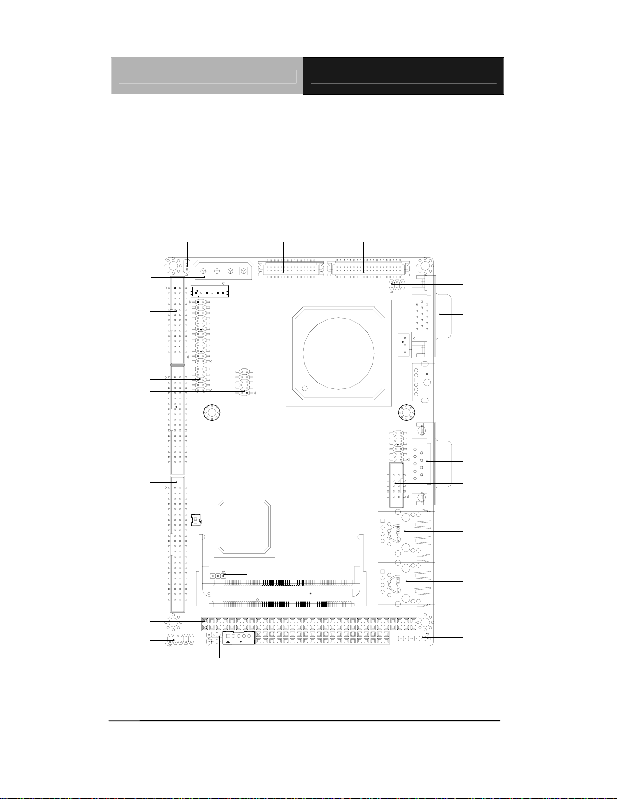
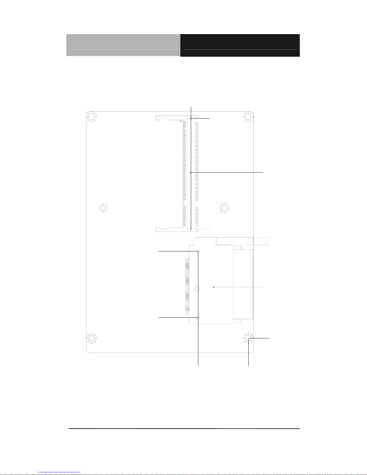
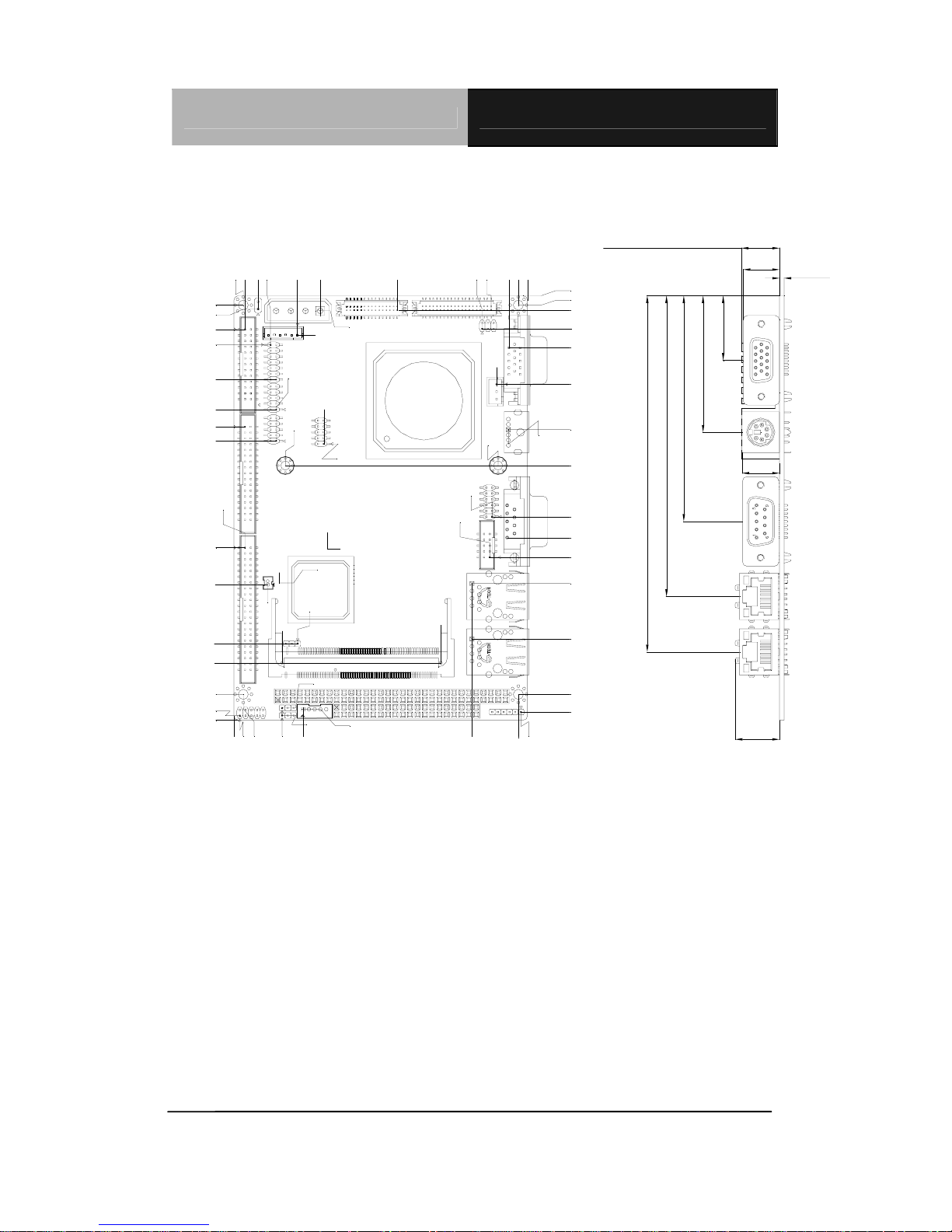
2.2 Jumpers, Connectors, and Mechanical Drawings
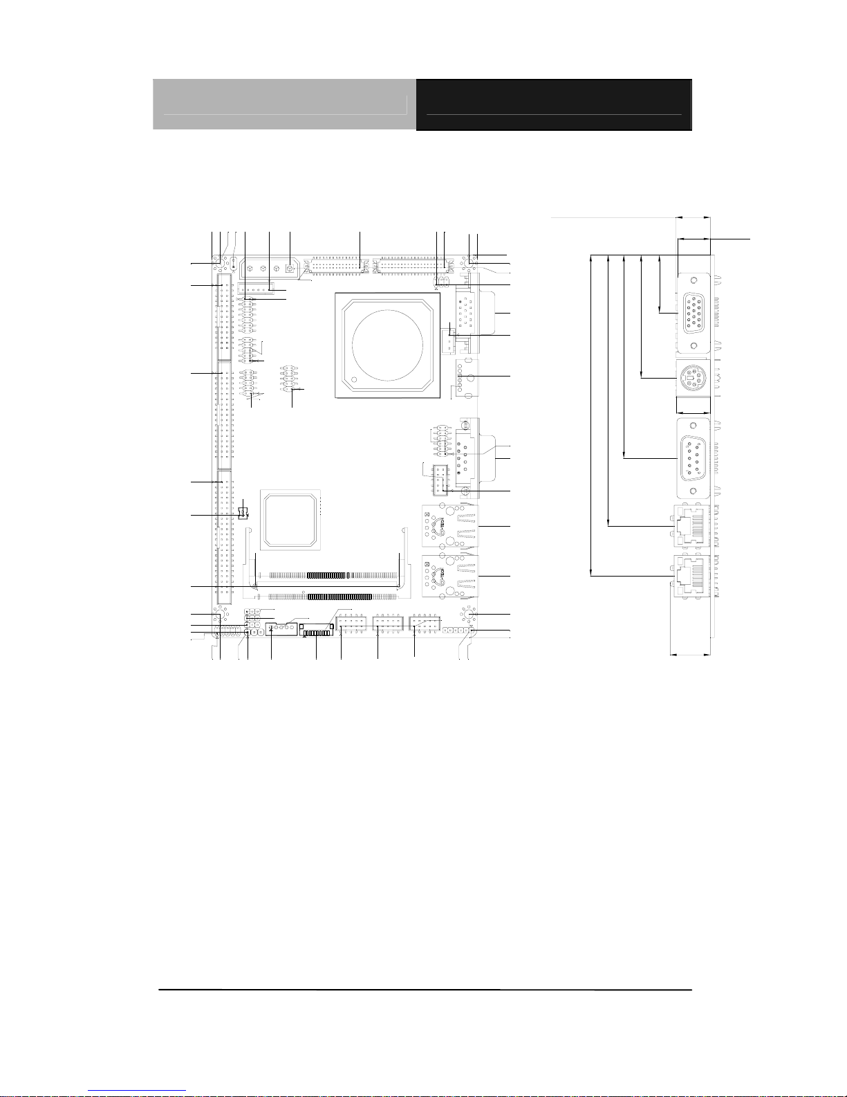
PCM-5315 Rev.A
Component Side
CN7
CN3
CN6
CN5
CN2
CN8
CN1
CN11
CN4
CN10
JP4
CN14
CN20
CN18
JP5
CN19
CN13
CN16
CN15
CN17
CN9
MPCI1
JP3
BAT1
CN22
JP2
JP6
CN12
JP1
CN21
Page 17
SubCompact Board PCM-5315
Chapter 2 Quick Installation Guide 2 - 4
Solder Side
DIMM1
CFD1
0.00
0.00
30.49
12.43
52.59
34.84
132.84
66.04
Page 18
SubCompact Board PCM-5315
Chapter 2 Quick Installation Guide 2 - 5
Mechanical Drawings
0.00
0.00
8.89
3.22
7.35
1.19
50.46
92.07
125.56
0.63
133.93
0.00
18.67
123.73
108.27
97.98
5.13
132.56
132.27
85.76
95.20
133.93
98.38
137.16
119.27
106.68
91.93
91.07
91.73
53.95
61.13
47.18
85.33
86.12
78.73
88.21
38.11
19.06
79.15
0.00
6.10
96.14
14.55
(1.60)
(12.55)
(13.00)
(15.35)
(22.22)
(46.99)
(77.67)
(103.50)
(122.55)
8.42
37.73
11.41
9.42
120.27
53.28
82.66
87.14
125.81
86.17
27.87
17.40
18.84
12.39
38.31
50.09
29.17
0.60
13.44
20.71
7.24
4.70
5.14
95.20
26.62
131.95
87.67
HEATSINK HEIGHT (13.20)
10.77
13.34
68.34
Page 19
SubCompact Board PCM-5315
Chapter 2 Quick Installation Guide 2 - 6 PCM
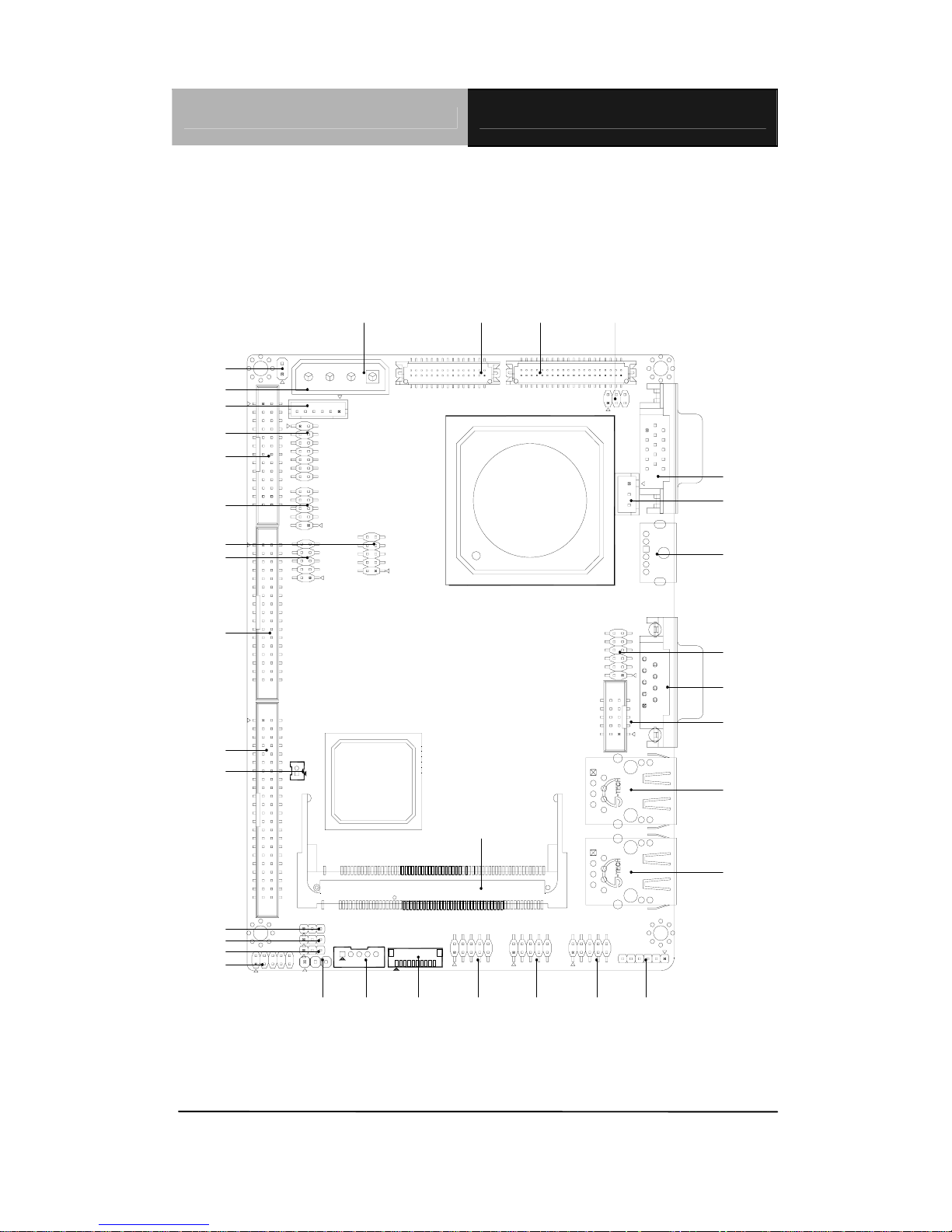
PCM-5315 Rev.B
Component Side
CN6
JP5
CN16
MPCI1
CN3
CN8
CN9
CN5
CN7
CN2
CN1
BAT1
JP3
JP2
JP7
CN4
CN21
JP1
JP6
CN22
CN26
CN24
CN25
CN23
CN17
CN15
CN13
CN19
CN18
CN14
CN20
CN10
CN9
CN12
JP4
Page 20
SubCompact Board PCM-5315
Chapter 2 Quick Installation Guide 2 - 7
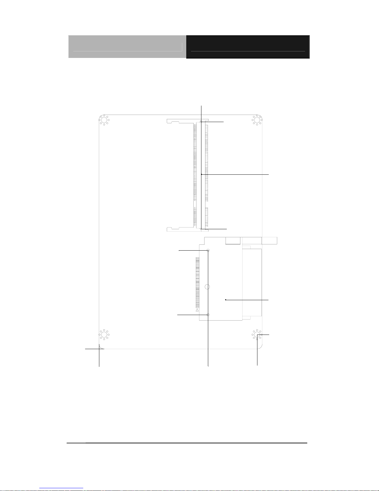
Solder Side
DIMM1
CFD1
8.89
98.38
30.49
12.43
52.53
34.84
132.84
66.04
0.00
0.00
Page 21
SubCompact Board PCM-5315
Chapter 2 Quick Installation Guide 2 - 8
Mechanical Drawings
8.89
96.14
95.20
74.31
60.21
46.11
36.78
19.44
10.49
10.27
0.00
1.13
6.10
0.00
14.61
33.66
59.49
47.18
61.13
91.07
114.94
133.93
125.75
106.60
95.20
87.67
85.76
53.28
26.62
5.13
0.00
3.23
137.16
133.93
125.56
123.73
120.27
96.71
27.37
85.92
84.27
11.81
92.07
50.46
37.85
8.59
10.77
13.34
68.34
1.02
1.52
4.06
6.86
7.41
0.00
0.60
9.41
18.67
131.95
132.22
82.66
91.73
86.12
85.33
11.47
5.01
5.84
4.56
(15.35)
(12.55)
(13.00)
98.37
(22.22)
(46.99)
(77.67)
(103.50)
(122.55)
HEATSINK HEIGHT (13.20)
Page 22

SubCompact Board PCM-5315
Chapter 2 Quick Installation Guide 2 - 9
2.3 List of Jumpers
The board has a number o f jumpers that allow you to configure
your system to suit your application.
The table below shows the f unction of each of the board' s
jumpers:
Label Function
JP1 AT/ATX Power Type Selection
JP2 CFD Master/Slave Selection
JP3 Clear CMOS
JP4 LCD Clock and LVDS Operating Voltage Selection
JP5 COM Ports RI/+5V/+12V Selection
JP6 Inverter Voltage Selection
JP7 CFD Voltage Selection (For Rev. B only)
Page 23

SubCompact Board PCM-5315
Chapter 2 Quick Installation Guide 2 - 10
2.4 List of Connectors
The board has a n umber of co nnectors that al low you to
configure your system to suit your application.
The table b elow shows the func tion of each of the boa rd’s
conn
ectors:
Note: For further information about mating connectors, please refer to
the appendix of the manual.
Label Function
CN1 IDE Hard Drive
CN2 Floppy
CN3 Parallel Port
CN4 Front Panel
CN5 USB Port #1 and Port #2
CN6 Digital I/O
CN7 Audio Input/Output/CD-in/MIC
CN8 ATX External 5VSB
CN9 4P Power Socket
CN10 LVDS LCD
CN11 PC/104 (For Rev. A only)
CN12 TTL LCD
CN13 Serial Port #2
CN14 System FAN
CN15 Ethernet 10/100 Base-TX RJ-45 Phone Jack #1
CN16 Ethernet 10/100 Base-TX RJ-45 Phone Jack #2
CN17 IrDA
Page 24

SubCompact Board PCM-5315
Chapter 2 Quick Installation Guide 2 - 11
CN18 Mini-Din PS/2
CN19 Serial Port #1
CN20 CRT Display
CN21 USB Port #3 and Port #4
CN22 LCD Inverter Voltage
CN23 Serial Port #3 (For Rev. B only)
CN24 Serial Port #5 (For Rev. B only)
CN25 Serial Port #4 (For Rev. B only)
CN26 Serial Port #6 (TTL/GPS) (For Rev. B only)
BAT1 External Battery
CFD1 Compact Flash Disk
MPCI1 Mini-PCI
DIMM1 DDR SODIMM Slot
Page 25
SubCompact Board PCM-5315
Chapter 2 Quick Installation Guide 2 - 12
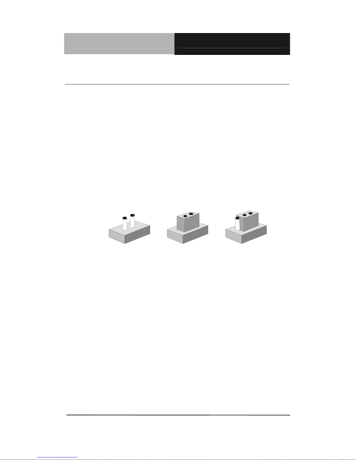
2.5 Setting Jumpers
You configure your card to match the needs of your application
by setting jumpers. A jumper is the simplest kind of electric switch.
It consists of two metal pins and a small metal clip (often
protected by a plastic cover) that slides over the pins to connect
them. To “close” a jumper you connect the pins with the clip.
To “open” a jumper you remove the clip. Sometimes a jumper will
have three p
ins, labeled 1, 2 and 3. In this case you would
connect either pins 1 and 2 or 2 and 3.
1
2
3
Open Clos ed Closed 2-3
A pair of needle-nose pliers may be helpful when working with
jumpers.
If you have any doubts about the best hardwa
re configuration for
your application, contact your lo cal distributor or sales
representative before yo u make any change. Generally, you
simply need a standard cable to make most connections.
Page 26

SubCompact Board PCM-5315
Chapter 2 Quick Installation Guide 2 - 13
2.6 AT/ATX Power Type Selection (JP1)
JP1 Function
1-2 ATX Power Supply
AT Power Supply (Default)
2.7 CFD Master/Slave Selection (JP2)
JP2 Function
1-2 Slave
2-3 Master (Default)
2.8 Clear CMOS (JP3)
JP3 Function
1-2 Normal (Default)
2-3 Clear CMOS
2.9 LCD Clock and LVDS Operating Voltage Selection (JP4)
Clock
JP4 Function
1-3 Normal (Default)
3-5 Shift Clock
LVDS Operating Voltage
JP4 Function
2-4 +5V
4-6 +3.3V (Default)
Page 27

SubCompact Board PCM-5315
Chapter 2 Quick Installation Guide 2 - 14
2.10 COM Ports RI/+5V/+12V Selection (JP5)
COM 1
JP5 Function
1-2 +12V
3-4 +5V
5-6 RI (Default)
COM 2
JP5 Function
7-8 +12V
9-10 +5V
11-12 RI (Default)
2.11 Inverter Voltage Selection (JP6)
JP6 Function
1-2 +5V (Default)
2-3 +12V
2.12 CFD Voltage Selection (JP7) (For Rev. B only)
JP7 Function
1-2 +5V (Default)
2-3 +3.3V
2.13 IDE Hard Drive Connector (CN1)
Pin Signal Pin Signal
1 RESET# 2 Ground
3 D7 4 D8
Page 28

SubCompact Board PCM-5315
Chapter 2 Quick Installation Guide 2 - 15
5 D6 6 D9
7 D5 8 D10
9 D4 10 D11
11 D3 12 D12
13 D2 14 D13
15 D1 16 D14
17 D0 18 D15
19 Ground 20 N.C.
21 DREQ 22 Ground
23 IOW# 24 Ground
25 IOR# 26 Ground
27 IORDY 28 Ground
29 DACK# 30 Ground
31 IRQ14 32 N.C.
33 DA1 34 PDIAG#
35 DA0 36 DA2
37 CS#1 38 CS#3
39 Active LED# 40 Ground
41 +5Volt. 42 +5Volt.
43 Ground 44 N.C.
Note: The IDE interface on PCM-5315 supports two IDE devices
including CF card. If you use a CF card, PCM-5315 allows one IDE
device.
2.14 Floppy Connector (CN2)
Pin Signal Pin Signal
1 Ground 2 DENSEL#
3 Ground 4 N.C.
5 Ground 6 N.C.
Page 29

SubCompact Board PCM-5315
Chapter 2 Quick Installation Guide 2 - 16
7 Ground 8 INDEX#
9 Ground 10 MTRA#
11 Ground 12 DRVB#
13 Ground 14 DRVA#
15 Ground 16 MTRB#
17 Ground 18 DIR#
19 Ground 20 STEP#
21 Ground 22 WDATA#
23 Ground 24 WGATE#
25 Ground 26 TRK0#
27 Ground 28 WPT#
29 N.C. 30 RDATA#
31 Ground 32 HDSEL#
33 N.C. 34 DSKCHG#
2.15 Parallel Port (CN3)
Pin Signal Pin Signal
1 STB# 2 AFD#
3 PTD0 4 ERR#
5 PTD1 6 PINIT#
7 PTD2 8 SLIN#
9 PTD3 10 Ground
11 PTD4 12 Ground
13 PTD5 14 Ground
15 PTD6 16 Ground
17 PTD7 18 Ground
19 ACK# 20 Ground
21 BUSY 22 Ground
23 PE 24 Ground
Page 30

SubCompact Board PCM-5315
Chapter 2 Quick Installation Guide 2 - 17
25 SLCT 26 N.C.
2.16 Front Panel Connector (CN4)
Pin Signal Pin Signal
1 Power On Button (-) 2 Power On Button (+)
3 IDE LED (-) 4 IDE LED (+)
5 External Buzzer (-) 6 External Buzzer (+)
7 Power LED (-) 8 Power LED (+)
9 Reset Switch (-) 10 Reset Switch (+)
2.17 USB Port #1 and Port #2 (CN5)
Pin Signal Pin Signal
1 VDD 2 Ground
3 D0- 4 Ground
5 D0+ 6 D1+
7 Ground 8 D1-
9 Ground 10 VDD
2.18 Digital I/O Connector (CN6)
Pin Signal Pin Signal
1 Port 1 2 Port 2
3 Port 3 4 Port 4
5 Port 5 6 Port 6
7 Port 7 8 Port 8
9 +5Volt. 10 Ground
DIO Address is 801H
BIOS Setting Connector
Definition
Address IT8712 GPIO Setting
DIO-1 CN6 Pin 1 Bit 7 U1 Pin 20 (GPIO 27)
Page 31

SubCompact Board PCM-5315
Chapter 2 Quick Installation Guide 2 - 18
DIO-2 CN6 Pin 2 Bit 6 U1 Pin 21 (GPIO 26)
DIO-3 CN6 Pin 3 Bit 5 U1 Pin 22 (GPIO 25)
DIO-4 CN6 Pin 4 Bit 4 U1 Pin 23 (GPIO 24)
DIO-5 CN6 Pin 5 Bit 3 U1 Pin 24 (GPIO 23)
DIO-6 CN6 Pin 6 Bit 2 U1 Pin 25 (GPIO 22)
DIO-7 CN6 Pin 7 Bit 1 U1 Pin 26 (GPIO 21)
DIO-8 CN6 Pin 8 Bit 0 U1 Pin 27 (GPIO 20)
2.19 Audio Input/Output/CDin/MIC (CN7)
Pin Signal Pin Signal
1 MIC 2 MIC_Vcc
3 Audio Ground 4 CD_GND
5 LINE_IN L 6 CD_L
7 LINE_IN R 8 CD_GND
9 Audio Ground 10 CD_R
11 LINE_OUT L 12 LINE_OUT R
13 Audio Ground 14 Audio Ground
2.20 ATX External 5VSB (CN8)
Pin Signal
1 N.C.
2 Ground
3 N.C.
4 Ground
5 PS_ON#
Page 32

SubCompact Board PCM-5315
Chapter 2 Quick Installation Guide 2 - 19
6 +5 Volt. Standby
2.21 4P Power Socket (CN9)
Pin Signal
1 +12 Volt.
2 Ground
3 Ground
4 +5 Volt.
2.22 LVDS LCD Connector (CN10)
Pin Signal Pin Signal
1 N.C. 2 N.C.
3 VDD 4 Ground
5 CLK- 6 CLK+
7 VDD 8 Ground
9 D0- 10 D0+
11 D1- 12 D1+
13 D2- 14 D2+
15 D3- 16 D3+
17 N.C. 18 N.C.
19 N.C. 20 N.C.
21 N.C. 22 N.C.
23 N.C. 24 N.C.
25 N.C. 26 N.C.
27 VDD 28 Ground
29 N.C. 30 N.C.
Page 33

SubCompact Board PCM-5315
Chapter 2 Quick Installation Guide 2 - 20
2.23 PC/104 (CN11) (For Rev. A only)
J1/P1
Pin A B
1 IOCHCK* GND
2 D7 RSTDRV
3 D6 +5V
4 D5 IRQ9
5 D4 -5V
6 D3 DRQ2
7 D2 -12V
8 D1 ENDXFR*
9 D0 +12V
10 IOCHRDY GND/KEY
11 AEN SMEMW*
12 A19 SMEMR*
13 A18 IOW*
14 A17 IOR*
15 A16 DACK3*
16 A15 DRQ3
17 A14 DACK1*
18 A13 DRQ1
19 A12 REFRESH*
20 A11 SYSCLK
21 A10 IRQ7
22 A9 IRQ6
23 A8 IRQ5
24 A7 IRQ4
25 A6 IRQ3
26 A5 DACK2*
27 A4 TC
28 A3 BALE
Page 34

SubCompact Board PCM-5315
Chapter 2 Quick Installation Guide 2 - 21
29 A2 +5V
30 A1 OSC
31 A0 GND
32 GND GND
J2/P2
Pin D C
1 GND GND
2 MEMCS16* SBHE*
3 IOCS16* LA23
4 IRQ10 LA22
5 IRQ11 LA21
6 IRQ12 LA20
7 IRQ15 LA19
8 IRQ14 LA18
9 DACK0* LA17
10 DRQ0 MEMR*
11 DACK5* MEMW*
12 DRQ5 SD8
13 DACK6* SD9
14 DRQ6 SD10
15 DACK7* SD11
16 DRQ7 SD12
17 +5V SD13
18 MASTER* SD14
19 GND SD15
20 GND GND/KEY
Note 1: PCM-5315 does not support PC/104 way legacy ISA-DMA
mode caused by AMD architecture.
Note 2:
Allocation Method of PC/104 Card for PCM-5315
PC/104 connector on PCM-5315 cannot automatically get
“Resource” when a new PC/104 card is added because of AMD
Page 35

SubCompact Board PCM-5315
Chapter 2 Quick Installation Guide 2 - 22
Geode’s architecture limitation. The following steps for setup
the resources manually for your reference.
1. Retrieve the resource of the PC/104 card. The
information is typically contained in the manual of the
PC/104 card.
2. Push a function key “Delete” to get into the BIOS.
3. Enable the resource of the device in BIOS setup.
4. Disable the resource of the dev
ice for which conflicts
the resource of the device mentioned above in BIOS
setup.
5. Save above BIOS setup and restart system.
6. Install the driver in operating system.
7. Open your Control Panel (click Start, then pick
Settings then
Control Panel). Double click the System
icon and choose the Device Manager tab. Find the
device for which you want to enable the device. Click
the plus sign (+) next to the various categories click on
the device you want to update, and then click on
"Resource" and then choose the resource what should
same as the hardware setup.
2.24 TTL LCD (CN12)
For 24-bit TFT LCD
Pin Signal Pin Signal
1 +5Volt. 2 +5Volt.
3 Ground 4 Ground
5 +3.3Volt. 6 +3.3Volt.
7 N.C. 8 Ground
9 B0 10 B1
11 B2 12 B3
13 B4 14 B5
15 B6 16 B7
17 G0 18 G1
19 G2 20 G3
21 G4 22 G5
23 G6 24 G7
Page 36

SubCompact Board PCM-5315
Chapter 2 Quick Installation Guide 2 - 23
25 R0 26 R1
27 R2 28 R3
29 R4 30 R5
31 R6 32 R7
33 Ground 34 Ground
35 Clock 36 VSYNC
37 DE 38 HSYNC
39 N.C. 40 N.C.
For 18-bit TFT LCD
Pin Signal Pin Signal
1 +5Volt. 2 +5Volt.
3 Ground 4 Ground
5 +3.3Volt. 6 +3.3Volt.
7 N.C. 8 Ground
9 N.C. 10 N.C.
11 B0 12 B1
13 B2 14 B3
15 B4 16 B5
17 N/C 18 N/C
19 G0 20 G1
21 G2 22 G3
23 G4 24 G5
25 N.C. 26 N.C.
27 R0 28 R1
29 R2 30 R3
31 R4 32 R5
33 Ground 34 Ground
35 Clock 36 VSYNC
Page 37

SubCompact Board PCM-5315
Chapter 2 Quick Installation Guide 2 - 24
37 DE 38 HSYNC
39 N.C. 40 N.C.
2.25 Serial Port #2 (CN13)
COM2/ RS-232 Mode
Pin Signal Pin Signal
1 DCDB 2 RXB
3 TXB 4 DTRB
5 Ground 6 DSRB
7 RTSB 8 CTSB
9 RIB (+5V/ +12V) 10 N.C.
COM2/ RS-422 Mode
Pin Signal Pin Signal
1 TXD- 2 RXD+
3 TXD+ 4 RXD-
5 Ground 6 N.C.
7 N.C. 8 N.C.
9 N.C. 10 N.C.
COM2/ RS-485 Mode
Pin Signal Pin Signal
1 TXD- 2 N.C.
3 TXD+ 4 N.C.
5 Ground 6 N.C.
7 N.C. 8 N.C.
9 N.C. 10 N.C.
2.26 Fan Connector (CN14)
Pin Signal
1 FAN Sense
Page 38

SubCompact Board PCM-5315
Chapter 2 Quick Installation Guide 2 - 25
2 +5 Volt.
3 Ground
2.27 Ethernet 10/100 Base-TX RJ-45 Phone Jack #1 (CN15)
Pin Signal Pin Signal
1 RXD- 2 RXD+
3 RCT 4 N.C.
5 N.C. 6 TCT
7 TXD- 8 TXD+
9 ACT_LED 10 LINK_LED
11 +3.3 Volt. 12 SPD_LED
13 Ground 14 Ground
2.28 Ethernet 10/100 Base-TX RJ-45 Phone Jack #2 (CN16)
Pin Signal Pin Signal
1 RXD- 2 RXD+
3 RCT 4 N.C.
5 N.C. 6 TCT
7 TXD- 8 TXD+
9 ACT_LED 10 LINK_LED
11 +3.3 Volt. 12 SPD_LED
13 Ground 14 Ground
2.29 IrDA Connector (CN17)
Pin Signal
1 +5 Volt.
2 CIR_TX (Option)
3 RX
Page 39

SubCompact Board PCM-5315
Chapter 2 Quick Installation Guide 2 - 26
4 Ground
5 TX
6 CIR_RX (Option)
2.30 Mini-DIN PS/2 Keyboard/ Mouse Connector (CN18)
Pin Signal Pin Signal
1 Keyboard Data 2 Keyboard Data
3 Ground 4 Ground
5 +5 Volt. 6 +5 Volt.
7 Shield 8 Shield
2.31 Serial Port #1 Connector (CN19)
COM 1
Pin Signal Pin Signal
1 DCDA 2 RXA
3 TXA 4 DTRA
5 Ground 6 DSRA
7 RTSA 8 CTSA
9 RIA (+5V/ +12V) 10 N.C.
2.32 CRT Display Connector (CN20)
Pin Signal Pin Signal
1 RED 9 +5 Volt.
2 GREEN 10 Ground
3 BLUE 11 N.C.
4 N.C. 12 DDCSDA
5 Ground 13 HSYNC
6 Ground 14 VSYNC
7 Ground 15 DDCSCL
Page 40

SubCompact Board PCM-5315
Chapter 2 Quick Installation Guide 2 - 27
8 Ground
2.33 USB Port #3 and Port #4 (CN21)
Pin Signal Pin Signal
1 VDD 2 Ground
3 D2- 4 Ground
5 D2+ 6 D3+
7 Ground 8 D3-
9 Ground 10 VDD
2.34 LCD Inverter Voltage (CN22)
Pin Signal
1 VCC
2 Backlight Control
3 Ground
4 Ground
5 Enable
2.35 Serial Port #3 (CN23) (For Rev.B only)
COM 3
Pin Signal Pin Signal
1 DCD3 2 RX3
3 TX3 4 DTR3
5 Ground 6 DSR3
7 RTS3 8 CTS3
9 RI3 10 N.C.
Page 41

SubCompact Board PCM-5315
Chapter 2 Quick Installation Guide 2 - 28
2.36 Serial Port #5 (CN24) (For Rev.B only)
COM 5
Pin Signal Pin Signal
1 DCD5 2 RX5
3 TX5 4 DTR5
5 Ground 6 DSR5
7 RTS5 8 CTS5
9 RI5 10 N.C.
Note: An APM Mode limitation, OS (Operating System) recognizes serial
port 5 & 6 of PCM-5315 Rev.B but is reverse. OS will reassign IRQ
and give sequence of serial port 5 & 6 after uninstalling all of serial ports
and second time boots in OS.
2.37 Serial Port #4 (CN25) (For Rev.B only)
COM 4
Pin Signal Pin Signal
1 DCD4 2 RX4
3 TX4 4 DTR4
5 Ground 6 DSR4
7 RTS4 8 CTS4
9 RI4 10 N.C.
2.38 Serial Port #6 (CN26) (TTL/GPS) (For Rev.B only)
COM 6
Pin Signal Pin Signal
1 N.C. 2 N.C.
3 Ground 4 N.C.
5 RX6 6 TX6
7 VBAT (+3 Volt.) 8 +3.3 Volt.
9 RESET# 10 Ground
Page 42

SubCompact Board PCM-5315
Chapter 2 Quick Installation Guide 2 - 29
Note: An APM Mode limitation, OS (Operating System) recognizes serial
port 5 & 6 of PCM-5315 Rev.B but is reverse. OS will reassign IRQ
and give sequence of serial port 5 & 6 after uninstalling all of serial ports
and second time boots in OS.
2.39 External Battery (BAT1)
Pin Signal
1 VBAT (+3 Volt.)
2 Ground
2.40 Compact Flash Disk Slot (CFD1)
Pin Signal Pin Signal
1 Ground 26 Ground
2 D3 27 D11
3 D4 28 D12
4 D5 29 D13
5 D6 30 D14
6 D7 31 D15
7 CS#1 32 CS#3
8 Ground 33 Ground
9 Ground 34 IOR#
10 Ground 35 IOW#
11 Ground 36 +5 Volt.
12 Ground 37 IRQ14
13 +5 Volt. 38 +5 Volt.
14 Ground 39 CSEL#
15 Ground 40 N.C.
16 Ground 41 RESET#
17 Ground 42 IORDY
18 DA2 43 DREQ
Page 43
SubCompact Board PCM-5315
Chapter 2 Quick Installation Guide 2 - 30
19 DA1 44 DACK#
20 DA0 45 DASP#
21 D0 46 PDIAG#
22 D1 47 D8
23 D2 48 D9
24 IO16# 49 D10
25 Ground 50 Ground
2.41 Mini-PCI Slot (MPCI1)
Standard Specification
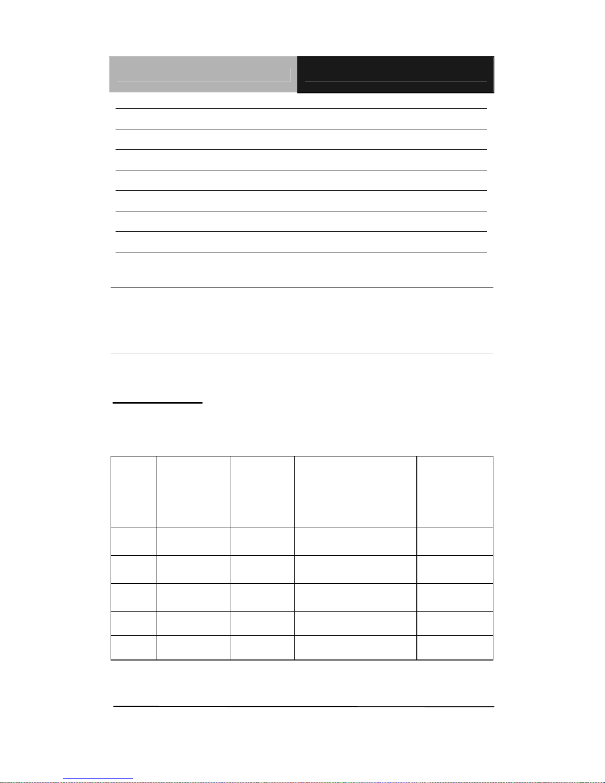
2.42 DDR SODIMM Slot (DIMM1)
Standard SODIMM Slot
Note from AMD:
Memory configurations supported. Onl
y one DIMM or SODIMM is
supported as long as the configuration requirements are met.
Devices Max
Memory
1
Max GLIU
Frequency
GLCP 4C00000Fh
Upper Bits/Lower Bits
GLMC
2000001 Ah
Bits【26:24】
4 512M 400MHz
F2F100FFh/
56960004h
4
8 1G 400MHz
F2F100FFh/
56960004h
4
4 512M 333MHz
F2F100FFh/
56960004h
3
8 1G 333MHz
F2F100FFh/ 56960004h
3
16 2G 333MHz
F2F100FFh/ 56960004h
3
1: Maximum memory is assuming 1Gbit devices.
Page 44
SubCompact Board PCM-5315
Chapter 2 Quick Installation Guide 2 - 31
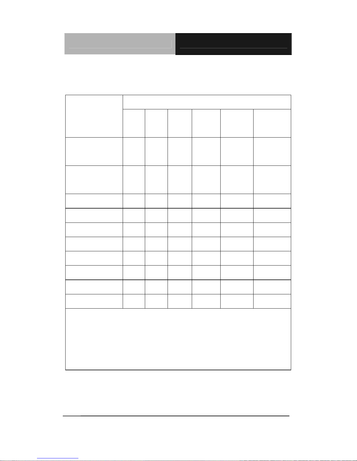
Below Table for China RoHS Requirements
产品中有毒有害物质或元素名称及含量
Main Board/ Daughter Board/ Backplane
有毒有害物质或元素
部件名称
铅
(Pb)汞 (Hg)镉 (Cd)
六价铬
(Cr(VI))
多溴联苯
(PBB)
多溴二苯醚
(PBDE)
印刷电路板
及其电子组件
× ○ ○ ○ ○ ○
外部信号
连接器及线材
× ○ ○ ○ ○ ○
O:表示该有毒有害物质在该部件所有均质材料中的含量均在
SJ/T 11363-2006 标准规定的限量要求以下。
X:表示该有毒有害物质至少在该部件的某一均质材料中的含量超出
SJ/T 11363-2006 标准规定
的限量要求。
备注:此产品所标示之环保使用期限,系指在一般正常使用状况下。
Page 45

SubCompact Board PCM-5315
Chapter 3 Award BIOS Setup 3-1
Chapter
Award
BIOS Setup
3
Page 46

SubCompact Board PCM-5315
Chapter 3 Award BIOS Setup 3-2
3.1 System Test and Initialization
These routines test and initialize board hardware. If the
routines encounter an error during the tests, you will either
hear a few short beeps or see an error message on the
screen. There are two kinds of errors: fatal and non-fatal. The
system can usually continue the boot up sequence with
non-fatal errors. Non-fatal error messages usually appear on
the screen along with the following instructions:
Press <F1> to RESUME
Write down the message and press the F1 key to continue
the boot up seque
nce.
System configuration verification
These routines check the current system configu
ration
against the values stored in the CMOS memory. If they do
not match, the program outputs an error message. You will
then need to run the BIOS setup program to set the
configuration information in memory.
There are three situations in which you will need to change
the CMOS settings:
1. You are
starting your system for the first time
2. You have changed the hardware attached to your system
3.
The CMOS memory has lost power and the configurat
ion
information has been erased.
The PCM-5315 CMOS memory has an integral lithium
battery
backup
for data retention.
However, you will need to
replace the complete unit when it finally runs down.
Page 47
SubCompact Board PCM-5315
Chapter 3 Award BIOS Setup 3-3
3.2 Award BIOS Setup
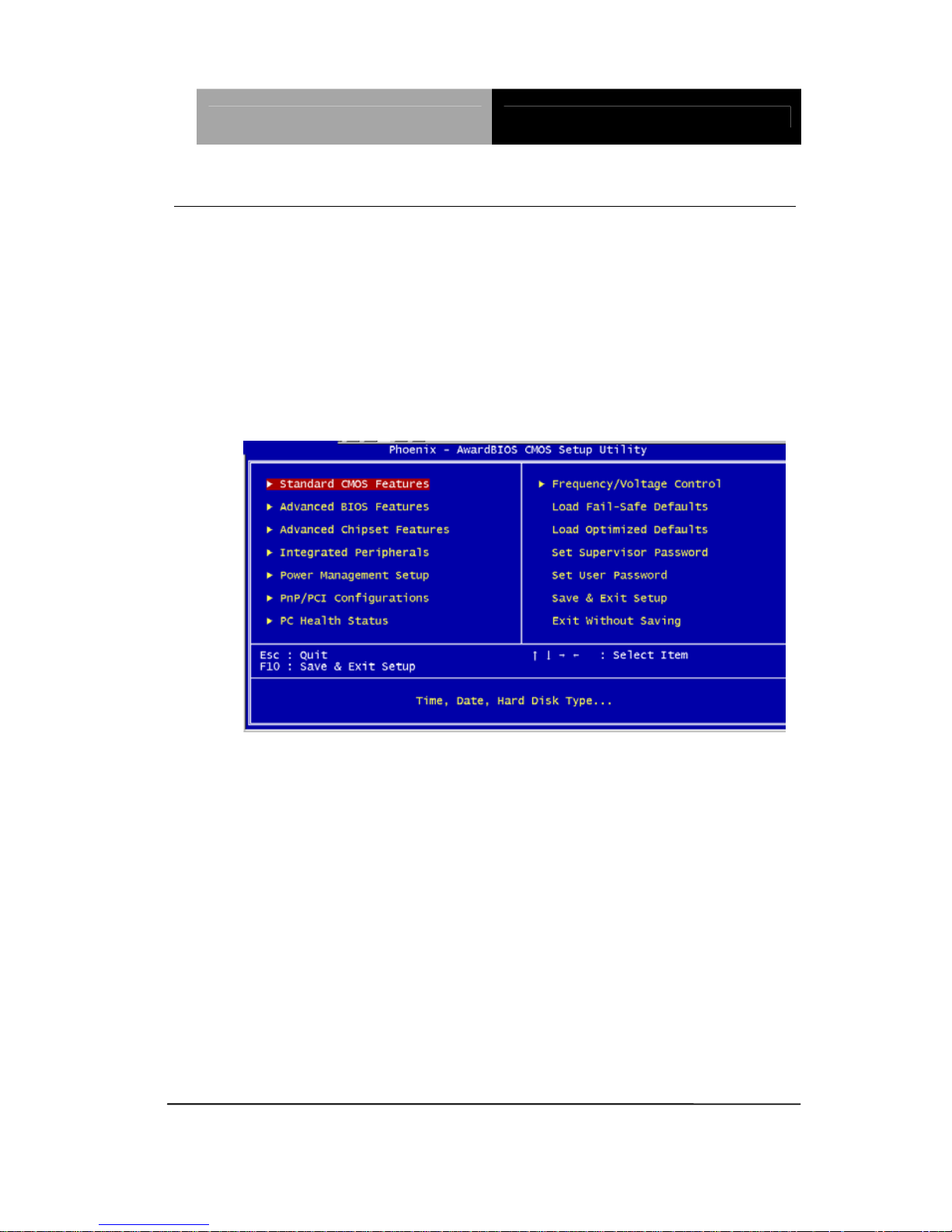
Awards BIOS ROM has a built-in Setup program that allows
users to modify the basic system configuration. This type of
information is stored in battery-backed CMOS RAM so that it
retains the Setup information when the power is turned off.
Entering Setup
Power on the computer and press <Del> immediately. This
will allow you to enter Setup.
Standard CMOS Features
Use this menu for basic system configuration. (Date, time,
IDE, etc.)
Advanced BIOS Features
Use this menu to set the advanced features available on your
system.
Page 48

SubCompact Board PCM-5315
Chapter 3 Award BIOS Setup 3-4
Advanced Chipset Features
Use this menu to change the values in the chipset registers
and optimize your system performance.
Integrated Peripherals
Use this menu to specify your settings for integrated
peripherals. (Primary slave, secondary slave, keyboard,
mouse etc.)
Power Management Setup
Use this menu to specify your settings for power
management. (HDD power down, power on by ring, KB wake
up, etc.)
PnP/PCI Configurations
This entry appears if your system supports PnP/PCI.
PC Health Status
This menu allows you to set the shutdown temperature for
your system.
Frequency/Voltage Control
Use this menu to specify your settings for auto detect
DIMM/PCI clock and spread spectrum.
Load Fail-Safe Defaults
Use this menu to load the BIOS default values for the
minimal/stable performance for your system to operate.
Page 49

SubCompact Board PCM-5315
Chapter 3 Award BIOS Setup 3-5
Load Optimized Defaults
Use this menu to load the BIOS default values that are
factory settings for optimal performance system operations.
While AWARD has designated the custom BIOS to maximize
performance, the factory has the right to change these
defaults to meet their needs.
Set Supervisor/User Password
Use this menu to set Supervisor/User Passwords.
Save and Exit Setup
Save CMOS value changes to CMOS and exit setup.
Exit Without Saving
Abandon all CMOS value changes and exit setup.
Page 50

SubCompact Board PCM-5315
Chapter 4 Driver Installation 4 - 1
Chapter
Driver
4
Installation
Page 51

SubCompact Board PCM-5315
Chapter 4 Driver Installation 4 - 2
4.1 Software Drivers
This chapter describes the operation and installation of the display
drivers supplied on the Supporting CD-ROM that are shipped with
your product. The onboard VGA adapter is based on the AMD LX
VGA Flat Panel/CRT controller. This controller offers a large set of
extended functions and higher resolutions. The purpose of the
enclosed software drivers is to take advantage of the extended
features of the AMD LX VGA Flat Panel/CRT controller.
Hardware Configuration
Some of the high-resolution drivers provided in this p
ackag
e will
work only in certain system configurations. If a driver does not
display correctly, try the following:
1. Change the display controller to CRT-only mode, rather than flat
panel o
r
simultaneous display mode. Some high-resolution
drivers will display correctly only in CRT mode.
2. If a high-resolution mode does not support your system, try to
use a lower-resolution mode. For example, 1024 x 768 mode will
not work on some systems, but 800 x 600 mode supports the
most.
Page 52

SubCompact Board PCM-5315
Chapter 4 Driver Installation 4 - 3
4.2 Necessary to Know
The instructions in this manual assume that you understand
elementary concepts of MS-DOS and the IBM Personal Computer.
Before you attempt to install any driver from the Supporting
CD-R
OM, you should:
Know how to copy files fro
m a CD-ROM to a directory on the
hard disk
Understand the MS-DOS directory structure
If you are uncertain ab
out any of these concepts, pleas
e refer
to the DOS or OS/2 user reference guides for more
information before you proceed with the installation.
Before you begin
The Supporting CD-ROM contains different drivers for
corre
sp
onding Windows OS, please choose the specific driver for
your Windows OS.
Page 53

SubCompact Board PCM-5315
Chapter 4 Driver Installation 4 - 4
4.3 Installing VGA Driver
Win XP / Win XPe VGA
Place the Driver CD-ROM into your CD-ROM drive
and follow the
steps below to install.
1. Click on Start button.
2. Click on Settings button.
3.
Click on Control Panel button.
4. Click on Sy
stem button.
5.
Select Hardw
are and click on Device Manager….
6. Double click on Video Controller (VGA
Compatible).
7. Click on Update Driver….
8.
Click on Next.
9. Select Sea
rch for a sui
table driver…, then click on Next.
10. Select Specify
a location, then click on Next.
11. Click on Brows
e.
12. Select “lx_wi
n” file from CD-ROM (Drivers/Step 1 –
LX_Graphics) then click on Open.
13. Click on OK.
14. Click on Next.
15. Click on Yes.
16.
Click on Finish.
Note: The user must install this system driver before install other
device drivers.
Page 54

SubCompact Board PCM-5315
Chapter 4 Driver Installation 4 - 5
4.4 Installing AES Driver
Win XP / Win XPe AES
Place the Driver CD-ROM into your CD-ROM drive
and follow the
steps below to install.
1. Click on Start button.
2. Click on Settings button.
3.
Click on Control Panel button.
4. Click on Sy
stem button.
5.
Select Hardw
are and click on Device Manager….
6. Double click on Entertainment Encry
ption/Decryption
Controller.
7. Click on Update Driver….
8.
Click on Next.
9. Select Sea
rch for a sui
table driver…, then click on Next.
10. Select Specify
a location, then click on Next.
11. Click on Brows
e.
12. Select “LXAES”
file from CD-ROM (Drivers/Step 2 – AES)
then click on Open.
13. Click on OK.
14. Click on Next.
15. Click on Fin
ish.
Page 55

SubCompact Board PCM-5315
Chapter 4 Driver Installation 4 - 6
4.5 Installing PCI to ISA Bridge Driver (For Rev.A only)
Win XP / Win XPe System
Place the Driver CD-ROM into your CD-ROM drive
and follow the
following steps to install.
1. Click on Start button.
2. Click on Settings button.
3.
Click on Control Panel button.
4. Click on Sy
stem button.
5.
Select Hardw
are and click on Device Manager….
6. Double click on Other
PCI Bridge Device
7. Click on Update Driver….
8.
Click on Next.
9. Select Sea
rch for a sui
table driver…, then click on Next.
10. Select Specify
a location, then click on Next.
11. Click on Brows
e.
12. Select “Ite” file from CD-ROM (Drivers/Step 3- PCI to ISA
Bridge for RevA
) then click on open.
13. Click on OK.
14. Click on Next.
15. Click on Fin
ish.
Page 56

SubCompact Board PCM-5315
Chapter 4 Driver Installation 4 - 7
4.6 Installing Ethernet Driver
1. Click on the Step 4 – Lan folder.
2. Double click on the Setup file located in the folder.
3.
Follow the instructions that the window shows.
4. The system will help you install the driv
er autom
atically.
4.7 Ethernet Software Configuration
The onboard Ethernet interface supports all major network
operating systems. I/O addresses and interrupts are easily
configured via the Insyde BIOS Setup. To configure the medium
type, to view the current configuration, or to run diagnostics, please
refer to the following instruction:
1. Power the main board on. Ensure that the RSET8139.EXE file
is located in the wo
rking drive.
2. At the prompt, type RSET8139.EXE and press <ENTER>.
The
Ethernet configuration program will then be displayed.
3. This simple screen shows all the available options for the
Ethernet interface. Just hig
hlight the option you wish to
change by using the Up and DOWN keys. To change a
selected item, press <ENTER>, and a screen will appear with
the available options. Highlight your option and press
<ENTER>. Each highlighted option has a helpful message
guide displayed at the bottom of the screen for additional
Page 57

SubCompact Board PCM-5315
Chapter 4 Driver Installation 4 - 8
information.
4. After you have made your selections and the configuration is
what you want, press <ES
C>. A prompt will appear asking if
you want to save the configuration. Press "Y" if you want to
save.
There are three very useful diagnostic functions offered in the
Ethernet Setup Menu a
s follows:
1. Run EEPROM test
2. Run Diagnostics on Board
3. Run Diagnostics on Network
Each option has its own display screen, which shows the format
and re
sult of any diagn
ostic tests undertaken.
4.8 Installing Audio Driver
Win XP / Win XPe Audio
Place the Driver CD-ROM into your CD-ROM drive
and follow the
steps below to install.
1. Click on Start button.
2. Click on Settings button.
3.
Click on Control Panel button.
4. Click on Sy
stem button.
5.
Select Hardw
are and click on Device Manager….
6. Double click on Multimedia Audio Controller.
7. Click on Update
Driver….
Page 58

SubCompact Board PCM-5315
Chapter 4 Driver Installation 4 - 9
8. Click on Next.
9. Select Search for a sui
table driver…, then click on Next.
10. Select Specify
a location, then click on Next.
11. Click on Brows
e.
12. Select “LXWDMAu
” file from CD-ROM (Drivers/Step 5 –
Audio) then click on Open.
13. Double click on the “bin”
folder
14. Click on OK.
15. Click on Nex
t.
16. Click on Yes.
17.
Click on Finish.
Page 59

SubCompact Board PCM-5315
Appendix A Programming the Watchdog Timer A - 1
Programming the
Appendix
A
Watchdog Timer
Page 60
SubCompact Board PCM-5315
Appendix A Programming the Watchdog Timer A - 2
A.1 Programming
PCM-5315 utilizes ITE 8712 chipset as its watchdog timer
controller. ( K version )
Below are the procedures to complete its configuration and
the intial watchdog timer program is also attached
based on which you can d
evelop customized program to fit
your application.
Configuring Sequence Description
After the ha rdware reset or power-on reset, the IT E 8712
enters the n
ormal mode with
all logi cal devices disabled
except KBC.
Page 61

SubCompact Board PCM-5315
Appendix A Programming the Watchdog Timer A - 3
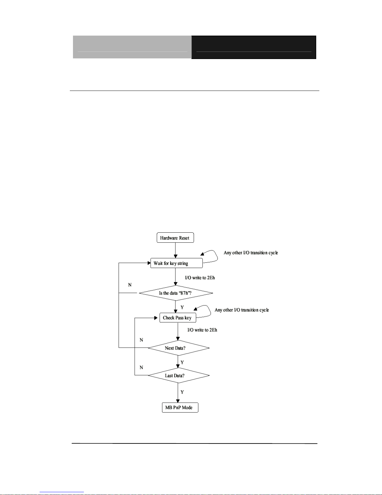
There are three steps to complete the configuration setup: (1)
Enter the MB PnP Mode; (2) Modify the data of configuration
registers; (3) Exit the MB PnP Mode. Undesired result may
occur if the MB PnP Mode is not exited normally.
(1) Enter the MB PnP Mode
To enter the MB PnP Mode, four special I/O write operations
are to be pe
rforme
d during Wait for Key state. To ensure the
initial state of the key-check logic, it is necessary to perform
four write opera-tions to the Special Address port (2EH). Two
different enter keys are provided to select configuration ports
(2Eh/2Fh) of the next step.
Address Port Data Port
87h, 01h, 55h, 55h: 2Eh 2Fh
(2) Modify the Data of the Registers
All configuration registers can be accessed
after entering the
MB PnP Mode. Before accessing a selected register, the
content of Index 07h must be changed to the LDN to which
the register belongs, except some Global registers.
(3) Exit the MB PnP Mode
Set bit 1 of the configure control regi
ster (Index=0
2h) to 1 to
exit the MB PnP Mode.
WatchDog Timer Configuration Registers
LDN Index R/W Reset Configuration Register or Action
All 02H W N/A Configuration Control
07H 71H R/W 00H WatchDog Timer Control Register
07H 72H R/W 00H WatchDog Timer Configuration Register
07H 73H R/W 00H WatchDog Timer Time-out Value (LSB)
Register
07H 74H R/W 00H WatchDog Timer Time-out Value (MSB)
Register
Page 62

SubCompact Board PCM-5315
Appendix A Programming the Watchdog Timer A - 4
Configure Control (Index=02h)
This register is write only. Its va lues are not sticky; that is to
say, a hardware re set will
automatically clear the bits, and
does not require the software to clear them.
Bit Description
7-2 Reserved
1 Returns to th e Wait for Key state. This bit is used when the
configuration sequence is completed.
0 Resets all logical devices and restores configuration registers
to their power-on states.
WatchDog Timer Control Register (Index=71h, Default=00h)
Bit Description
7 WDT is reset upon a CIR interrupt
6 WDT is reset upon a KBC (Mouse) interrupt
5 WDT is reset upon a KBC (Keyboard) interrupt
4 WDT is reset upon a read or a write to the Game port ba se
address
3-2 Reserved
1 Force Time-out. This bit is self-clearing
0 WDT status
1: WDT value reaches 0
0: WDT value is not 0
WatchDog Timer Configuration Register (Index=72h,
Default=00h)
Bit Description
7 WDT Time-out value select
1: Second
0: Minute
6 WDT output through KRST (pulse) enable
5 WDT Time-out value Extra select
1: 4s.
0: Determine by WDT Time-out value select (bit7 of th is
register)
Page 63

SubCompact Board PCM-5315
Appendix A Programming the Watchdog Timer A - 5
4 WDT output through PWROK1/PWROK2 (pulse) enable
3 Select the interrupt level
note
for WDT
WatchDog Timer Time-out Value (LSB) Register (Index=73h,
Default=00h)
Bit Description
7-0 WDT Time-out value 7-0
WatchDog Timer Time-out Value (MSB) Register (Index=74h,
Default=00h)
Bit Description
7-0 WDT Time-out value 15-8
A.2 ITE8712 Watchdog Timer Initial Program
.MODEL SMALL
.CODE
Main:
CALL Enter_Configuration_mode
CALL Check_Chip
mov cl, 7
call Set_Logic_Device
;time setting
mov cl, 10 ; 10 Sec
dec al
Page 64

SubCompact Board PCM-5315
Appendix A Programming the Watchdog Timer A - 6
Watch_Dog_Setting:
;Timer setting
mov al, cl
mov cl, 73h
call Superio_Set_Reg
;Clear by keyboard or mouse interrupt
mov al, 0f0h
mov cl, 71h
call Superio_Set_Reg
;unit is second.
mov al, 0C0H
mov cl, 72h
call Superio_Set_Reg
; game port enable
mov cl, 9
call Set_Logic_Device
Initial_OK:
CALL Exit_Configuration_mode
MOV AH,4Ch
INT 21h
Enter_Configuration_Mode PROC NEAR
MOV SI,WORD PTR CS:[Offset Cfg_Port]
Page 65

SubCompact Board PCM-5315
Appendix A Programming the Watchdog Timer A - 7
MOV DX,02Eh
MOV CX,04h
Init_1:
MOV AL,BYTE PTR CS:[SI]
OUT DX,AL
INC SI
LOOP Init_1
RET
Enter_Configuration_Mode ENDP
Exit_Configuration_Mode PROC NEAR
MOV AX,0202h
CALL Write_Configuration_Data
RET
Exit_Configuration_Mode ENDP
Check_Chip PROC NEAR
MOV AL,20h
CALL Read_Configuration_Data
CMP AL,87h
JNE Not_Initial
MOV AL,21h
CALL Read_Configuration_Data
Page 66

SubCompact Board PCM-5315
Appendix A Programming the Watchdog Timer A - 8
CMP AL,12h
JNE Not_Initial
Need_Initial:
STC
RET
Not_Initial:
CLC
RET
Check_Chip ENDP
Read_Configuration_Data PROC NEAR
MOV DX,WORD PTR CS:[Cfg_Port+04h]
OUT DX,AL
MOV DX,WORD PTR CS:[Cfg_Port+06h]
IN AL,DX
RET
Read_Configuration_Data ENDP
Write_Configuration_Data PROC NEAR
MOV DX,WORD PTR CS:[Cfg_Port+04h]
OUT DX,AL
XCHG AL,AH
MOV DX,WORD PTR CS:[Cfg_Port+06h]
OUT DX,AL
RET
Page 67

SubCompact Board PCM-5315
Appendix A Programming the Watchdog Timer A - 9
Write_Configuration_Data ENDP
Superio_Set_Reg proc near
push ax
MOV DX,WORD PTR CS:[Cfg_Port+04h]
mov al,cl
out dx,al
pop ax
inc dx
out dx,al
ret
Superio_Set_Reg endp.Set_Logic_Device proc near
Set_Logic_Device pro c near
push ax
push cx
xchg al,cl
mov cl,07h
call Superio_Set_Reg
pop cx
pop ax
ret
Set_Logic_Device endp
;Select 02Eh->Index Port, 02Fh->Data Port
Page 68

SubCompact Board PCM-5315
Appendix A Programming the Watchdog Timer A - 10
Cfg_Port DB 087h,001h,055h,055h
DW 02Eh,02Fh
END Main
Note: Interrupt level mapping
0Fh-Dh: not valid
0Ch: IRQ12
.
.
03h: IRQ3
02h: not valid
01h: IRQ1
00h: no interrupt selected
Page 69

SubCompact Board PCM-5315
Appendix B I/O Information B - 1
I/O Information
Appendix
B
Page 70
SubCompact Board PCM-5315
Appendix B I/O Information B - 2
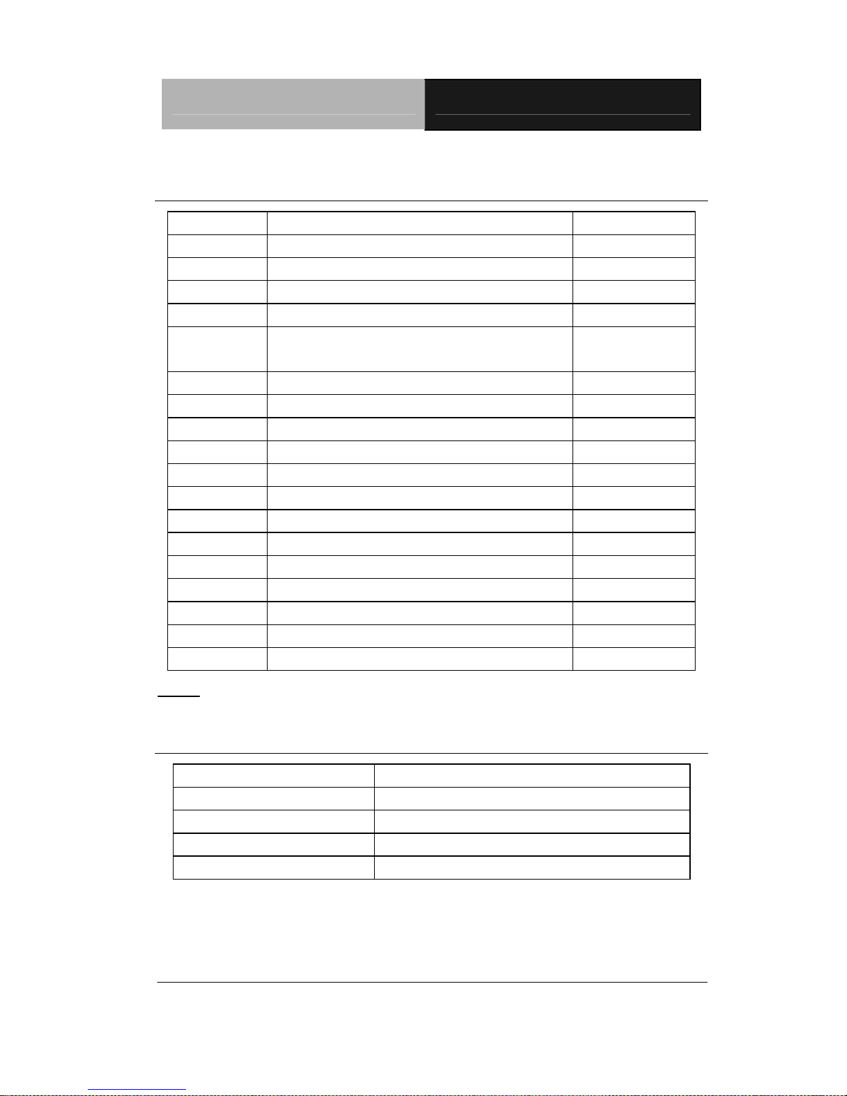
B.1 I/O Address Map
Address Description User Address
000-01F DMA Controller #1 000-000F
020-03F Interrupt Controller #1, Master 020-021
040-05F System Time 040-043
060-06F 8042 (Keyboard Controller) 060-064
070-07F
Real time C lock, NMI (non-maskable
Interrupt) Mask
070-073
080-09F DMA Page Register 080-08F
0A0-0BF Interrupt Controller #2 0A0-0A1
0C0-0DF DMA Controller #2 0C0-0DF
0F0-0FF Math Coprocessor 0F0-0FF
1F0-1F7 Primary IDE Channel 1F0-1F7
2E8-2EF* Serial Port 4 2E8-2EF
2F8-2FF Serial Port 2 2F8-2FF
378-37F Parallel Printer Port 1 378-37F
3B0-3DF EGA / VGA card 3B0-3DF
3E8-3EF* Serial Port 3 3E8-3EF
3F8-3FF Serial Port 1 3F8-3FF
4E0-4E7* Serial Port 5 4E0-4E7
4E8-4EF* Serial Port 6 4E8-4EF
Note: The Serial Port 3~6 are for Rev.B only.
B.2 1st MB Memory Address Map
Memory Address Description
00000-9FFFF System memory
A0000-BFFFF VGA buffer
C0000-CBFFF VGA BIOS
E0000-FFFFF System BIOS
Page 71
SubCompact Board PCM-5315
Appendix B I/O Information B - 3
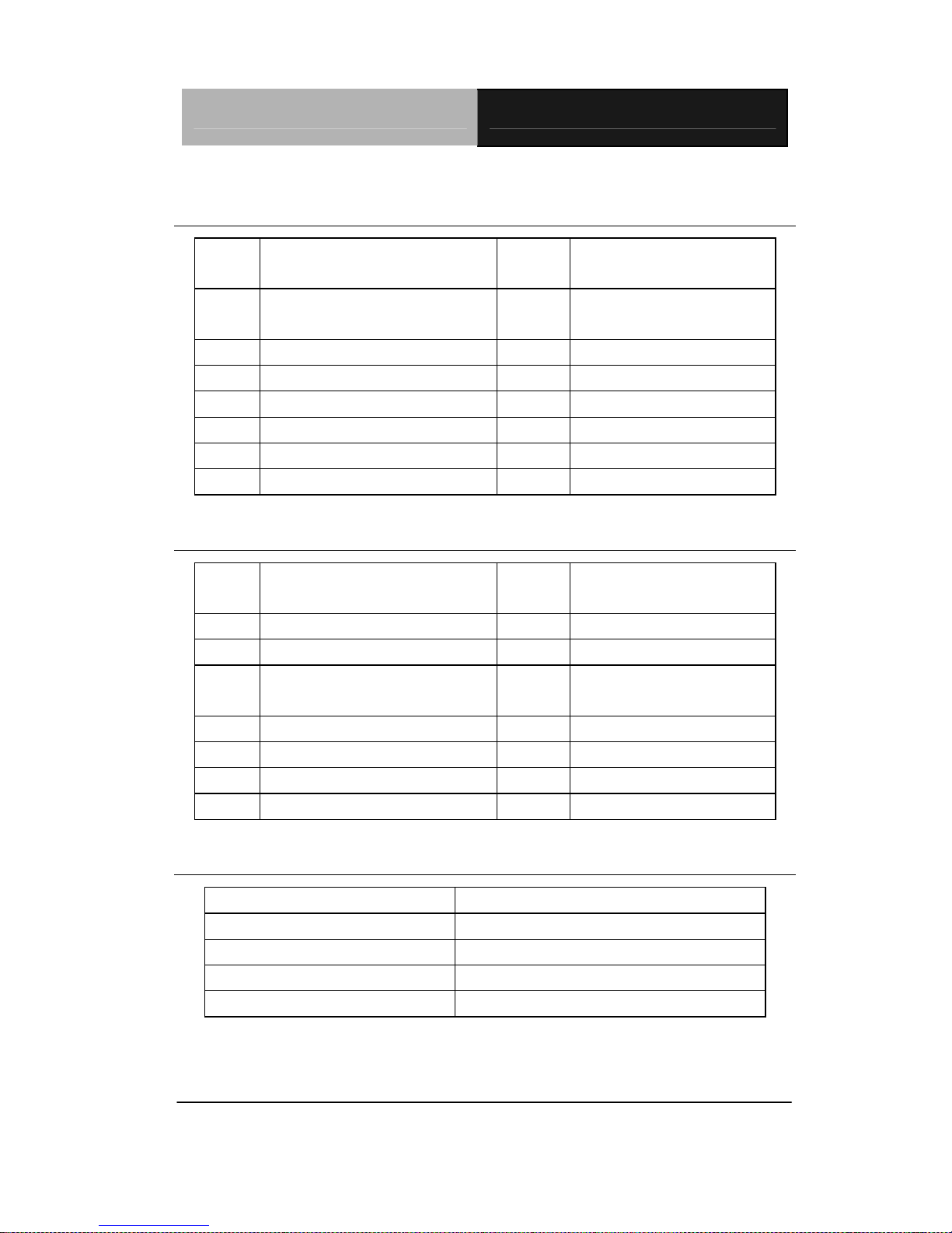
B.3 IRQ Mapping Chart for Rev.A
IRQ0 System Timer IRQ8 System CMOS / Real
time clock
IRQ1 Keyboard IRQ9 Microsoft ACPI –
Compliant system
IRQ2 Cascade to IRQ Controller IRQ10 Unused
IRQ3 COM2 IRQ11 Unused
IRQ4 COM1 IRQ12 PS/2 mouse
IRQ5 Unused IRQ13 FPU
IRQ6 Floppy IRQ14 Primary IDE
IRQ7 Printer IRQ15 Reserved
B.4 IRQ Mapping Chart for Rev.B
IRQ0 System Timer IRQ8 System CMOS / Real
time clock
IRQ1 Keyboard IRQ9 COM6
IRQ2 Cascade to IRQ Controller IRQ10 COM3
IRQ3 COM2 IRQ11 Microsoft ACPI –
Compliant system
IRQ4 COM1 IRQ12 PS/2 mouse
IRQ5 COM4 IRQ13 FPU
IRQ6 Floppy IRQ14 Primary IDE
IRQ7 COM5/ Printer IRQ15 Reserved
B.5 DMA Channel Assignments
DMA Channel Function
0 Available
1 Available
2 Floppy
3 Available
Page 72

SubCompact Board PCM-5315
Appendix C Mating Connector C - 1
Mating Connector
Appendix
C
Page 73
SubCompact Board PCM-5315
Appendix C Mating Connector C - 2
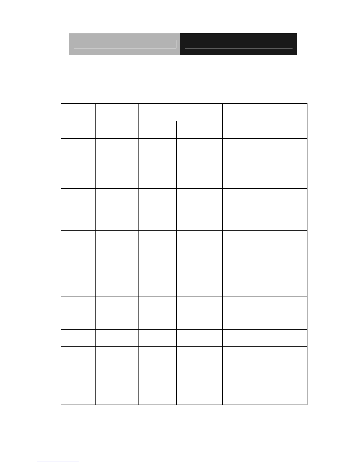
C.1 List of Mating Connectors and Cables
The table notes mating connectors and available cables.
Mating Connector Connector
Label
Function
Vendor Model no
Available
Cable
Cable P/N
CN1 IDE
Connector
MOLEX 87568-4463 IDE
Cable
17014405
00
CN2 Floppy
Connector
HR A2016H-N-2X
17P-A
Floppy
Disk
Drive
Cable
1701340600
CN3 Parallel Port
Connector
HR A2016H-N-2X
13P-A
Parallel
Port
Cable
1701260201
CN4 Front Panel
Connector
Neltron 2026B-10 N/A
CN5 USB
Connector
Neltron 2026B-10 USB
Cable
17091002
01
or 170910020D
(for PCM
-5315W1)
CN6 Digital I/O
Connector
Neltron 2026B-10 N/A
CN7 Audio
Connector
Catch
Electronics
052-D20014P
Audio
Cable
1700140510
CN8 ATX External
5VSB
Connector
Catch
Electronics
2418HJ-06 ATX
External
5VSB
Cable
1702200205
CN9 4P Power
Connnector
Neltron 8980-04 N/A
CN10 LVDS LCD
Connector
HIROSE DF13-30DS-1
.25C
N/A
CN12 TTL LCD
Connector
HIROSE DF13-40DS-1
.25C
N/A
CN13 Serial
Port 2
Connector
Neltron 2026B-1
0 Serial
Port
Cable
170110
0207
Page 74
SubCompact Board PCM-5315
Appendix C Mating Connector C - 3
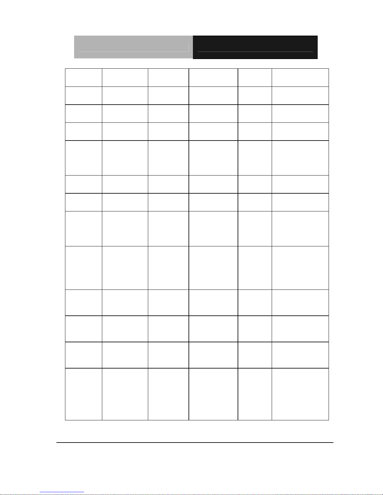
CN14 System FAN
Connector
Hobase
Technology
2503-H-3 N/A
CN15 Ethernet
Connector
Neltron 7001-8P8C N/A
CN16 Ethernet
Connector
Neltron 7001-8P8C N/A
CN17 IrDA
Connector
Neltron 2026A-06 N/A
CN18 Mini-Din
PS/2
Connector
Catch
Electronics
MD06F011
121
Keyboar
d &
Mouse
Cable
1700060192
CN19 Serial Port 1
Connector
AMP 707-09F N/A
CN20 CRT Display
Connector
Hobase
Technology
708HD-15M N/A
CN21 USB
Connector
Neltron 2026B-10 USB
Cable
1709100201 or
170910020D
(for PCM
-5315W1)
CN22 LCD Inverter
Voltage
Catch
Electronics
2.0mm pitch 5
pin (CATCH
HS-5P-2.0,
JST PHR-5 or
compatible)
LCD
Inverter
Cable
N/A
CN23
(Rev.B)
Serial
Port 3
Connector
Neltron 2026B-1
0 Serial
Port
Cable
170110
0207
CN24
(Rev.B)
Serial
Port 5
Connector
Neltron 2026B-1
0 Serial
Port
Cable
170110
0207
CN25
(Rev.B)
Serial
Port 4
Connector
Neltron 2026B-1
0 Serial
Port
Cable
170110
0207
CN26
(Rev.B)
Serial
Port 6
Connector
Catch
Electronics
1.0mm pitch
10 pin
(CATCH
HS-10P-1.0
or
compatible)
N/A N/A
 Loading...