

Page 1
Quick Installation Guide
PCM-4896L Installation Guide 1
Notice:
This guide is designed for experienced users to
setup the system within the shortest time. For
detailed information, please always refer to the
electronic user's manual.
Safety Precautions
PCM-4896L
All-in-One Single Board NS Geode GX1 computer with LCD, Ether-
net, Audio, & 4 COMs
Part no. 2007489605 2nd Ed. Printed in Taiwan May 2002
Quick Installation Guide
Warning! Always completely disconnect the power cord from
your chassis whenever you work with the hardware.
Do not make connections while the power is on.
Sensitive electronic components can be damaged
by sudden power surges. Only experienced electronics personnel should open the PC chassis.
Caution! Always ground yourself to remove any static charge
before touching the CPU card. Modern electronic
devices are very sensitive to static electric charges. As a safety precaution, use a grounding wrist
strap at all times. Place all electronic components
in a static-dissipative surface or static-shielded bag
when they are not in the chassis.
PCM-4896L
Page 2
PCM-4896L
2 PCM-4896L Installation Guide
BC-599/596
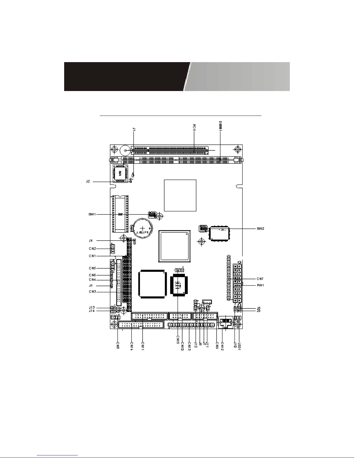
Locating Jumpers and Connectors
Page 3
Quick Installation Guide
PCM-4896L Installation Guide 3
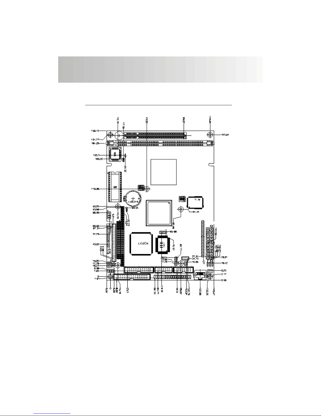
Mechanical Drawing
Page 4

PCM-4896L
4 PCM-4896L Installation Guide
BC-599/596
Jumpers and Connectors
Connectors on the board link themselves to the external devices
such as hard disk drives, a keyboard, or floppy drives. In addition,
the board has a number of jumpers that allow you to configure your
system to suit your application.
The following tables list the function of each jumper and connector
on the board.
Jumpers
Label Function
J1 Internal buzzer select
J4 Clear CMOS
J5 ATX soft-power switch connector
J6 Audio output select
J8 LCD driving voltage select
J9 LCD clock select
J10 Audio Power
J11 COM4 RI pin voltage select
J12 COM3 RI pin voltage select
J13 COM2 RS232/422/485 setting
J14 COM2 RS232/422/485 selection
SW1 (1~3) CPU frequency ratio
SW1 (5, 6) DOC address select
SW2 (1) CPU clock select
Page 5

Quick Installation Guide
PCM-4896L Installation Guide 5
Connectors
Label Function
CN 1 PC/104 connector
CN 2 USB ports connector
CN 4 IDE drive connector
CN 5 Front panel connector
CN6 IrDA connector
CN 7 LCD display connector
CN 8 Keyboard and PS/2 mouse connector
CN 9 VGA display connector
CN10 Audio connector
CN11 Printer port connector
CN12 100Base-Tx Ethernet connector
CN13 Serial ports connector
CN14 Floppy dirve connector
CN15 Digital I/O connector
PW1 ATX power connector
J7 CD-ROM signal input connector
LED1 Ethernet Tx/Rx/Link LED connector
U4 DiskOnChip socket
Page 6
PCM-4896L
6 PCM-4896L Installation Guide
BC-599/596
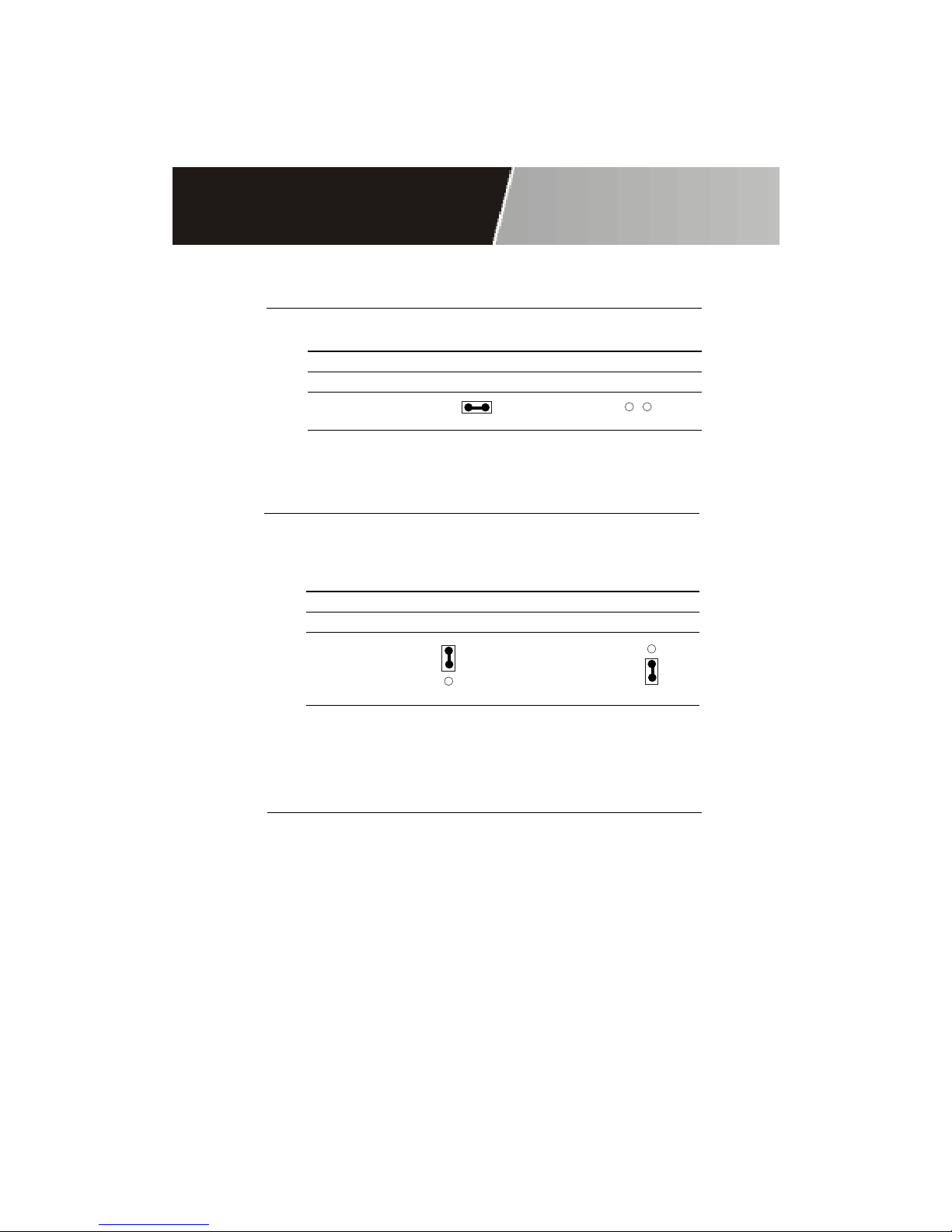
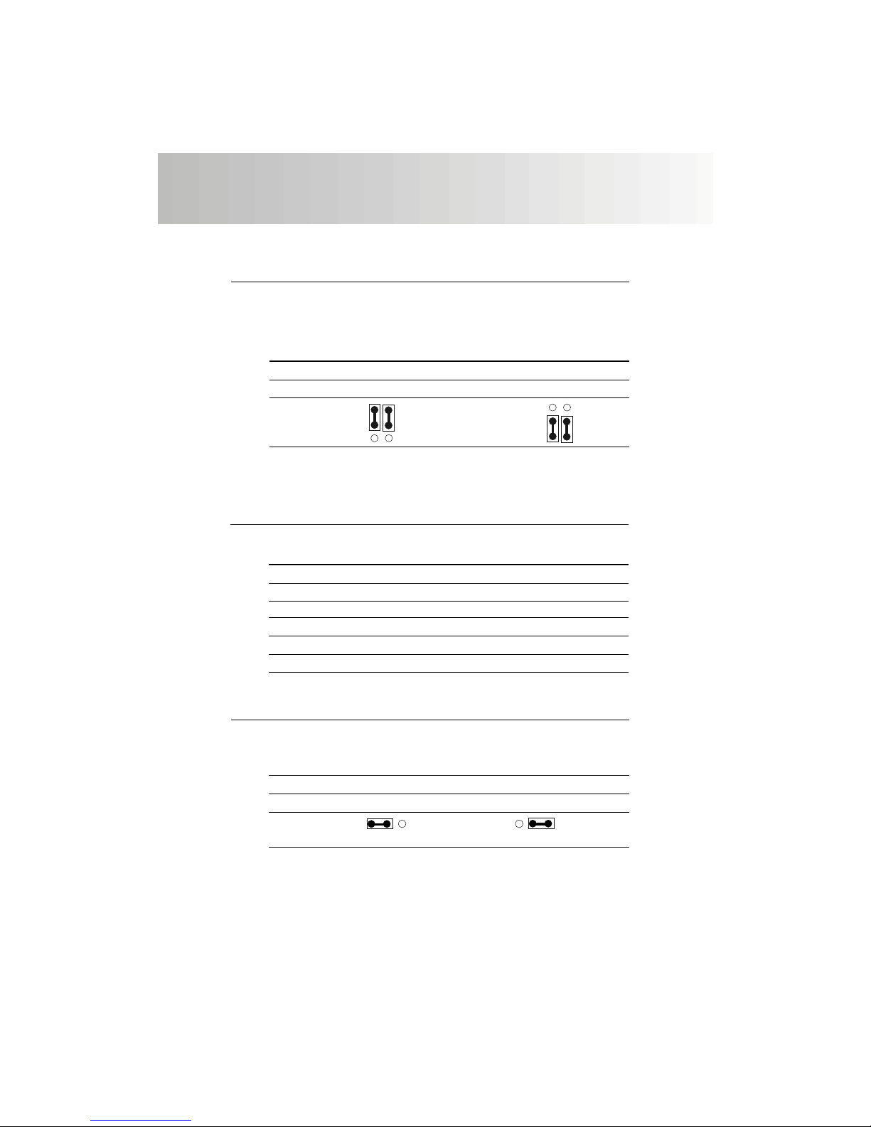
Internal Buzzer Select (J1)
Internal Buzzer Select (J1)
Internal Buzzer External Speaker
Clear CMOS (J4)
You can use J4 to clear the CMOS data if necessary. To reset the
CMOS data, set J4 to 2-3 closed for just a few seconds, and then
move the jumper back to 1-2 closed.
Clear CMOS (J4)
Protect* Clear CMOS
J4
*default
1
2
3
1
2
3
ATX Soft-Power Switch Connector (J5)
The A TX Soft-Power switch connector is a 2-pin header . Please plug
the power switch cable from your system to the Soft-Power switch
connector marked J5.
J1
1 2
1 2
Page 7
Quick Installation Guide
PCM-4896L Installation Guide 7
CD Audio Connector (J7)
This connector is used to connect to a CD audio cable.
CD Audio Connector (J7)
Pin Signal
1 GND
2 CD_L
3 GND
4 CD_R
J8
LCD Driving Voltage Select (J8)
You can select the LCD connector CN7 (pin 5 and pin 6) driving
voltage by setting J8. The configurations are as follows:
LCD Driving Voltage Select (J8)
5V 3.3V *
*default
1 2 3 1 2 3
2 1
4 3
6 5
2 1
4 3
6 5
Audio Output Select (J6)
You can select the output mode of onboard audio connector (CN10)
by setting J6.
"Speaker out" is the output signal amplified by onboard amplifier
Audio Output Select (J6)
Line out* Speaker out
J6
*default
Page 8
PCM-4896L
8 PCM-4896L Installation Guide
BC-599/596
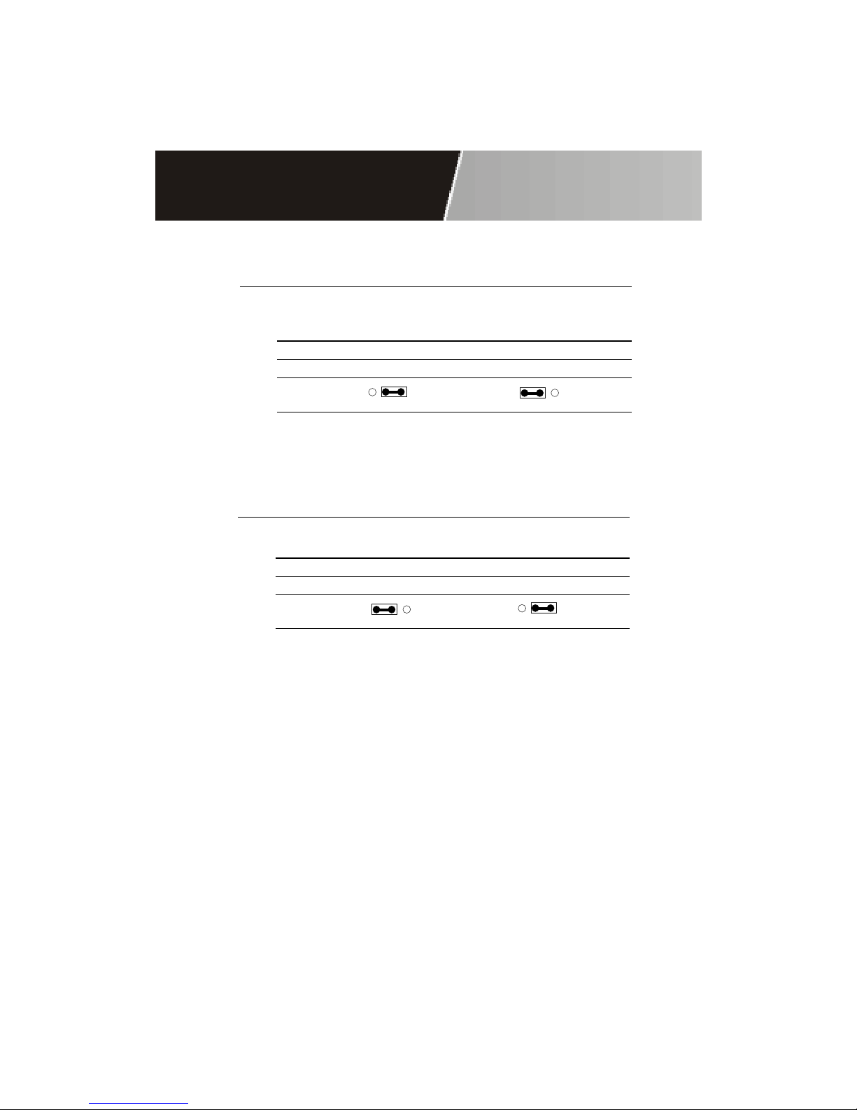
Audio Power Setting (J10)
The default setting is pin1 and pin 2 closed to offer audio power .
Audio Power Setting (J10)
Vcc * Reserved
*default
J10
1 2 3
1 2 3
LCD Clock Signal Select (J9)
You can select the LCD control signal by setting J9. The following
chart shows the available options.
LCD Clock Signal Select (J9)
SHF CLK * ASHF CLK
*default
J9
1 2 3
1 2 3
Page 9
Quick Installation Guide
PCM-4896L Installation Guide 9
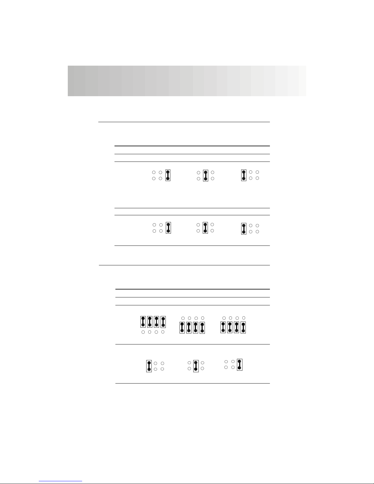
COM3/COM4 RI Pin Voltage Select
(J12, J11)
The 9th pin of COM3 and COM4 (9-pin D-sub connector) can be
selected as RI, +5V , or +12V by setting J12 & J1 1.
COM3 RI Pin Setting (J12)
RI* +5V +12V
J12
COM4 RI Pin Setting (J11)
RI * +5V +12V
J11
*default
1 3 5
2 4 6
1 3 5
2 4 6
1 3 5
2 4 6
1 3 5
2 4 6
1 3 5
2 4 6
1 3 5
2 4 6
COM2 RS-232/422/485 Select (J13, J14)
The PCM-4896 COM2 serial port can be selected as RS-232, RS-422,
or RS-485 by setting J13 & J14.
COM2 Select (J13, J14)
RS-232* RS-422 RS-485
J13
J14
*default
1 4 7 10
3 6 9 12
1 4 7 10
3 6 9 12
1 4 7 10
3 6 9 12
1 3 5
2 4 6
1 3 5
2 4 6
1 3 5
2 4 6
Page 10
PCM-4896L
10 PCM-4896L Installation Guide
BC-599/596
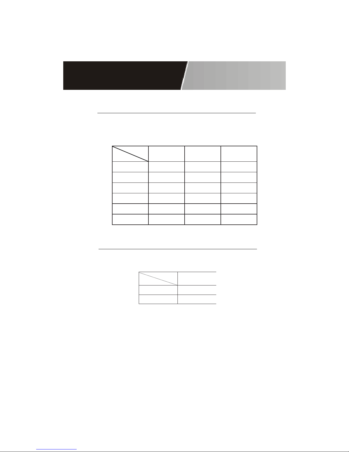
SW1 (1~3) CPU Frequency Ratio
SW2 (1) CPU Clock Select
Y ou can configure the CPU external clock to 33MHz or 30MHz by
setting SW2(1).
123
X4NONONO
X5NOFFOFFO
X6FFONOFFO
X7FFOFFONO
X9NOFFONO
X01NONOFFO
SW1
Ratio
1
zHM33NO
zHM03FFO
SW2
Freq.
The GX1 CPU core frequency = CPU frequency ratio (4~10X) * External CPU clock (33 or 30MHz). the following table shows the available
cnfigurations.
Any CPU setting change is strongly prohibited!!
Page 11
Quick Installation Guide
PCM-4896L Installation Guide 11
GX1 CPU Jumper Setting Examples
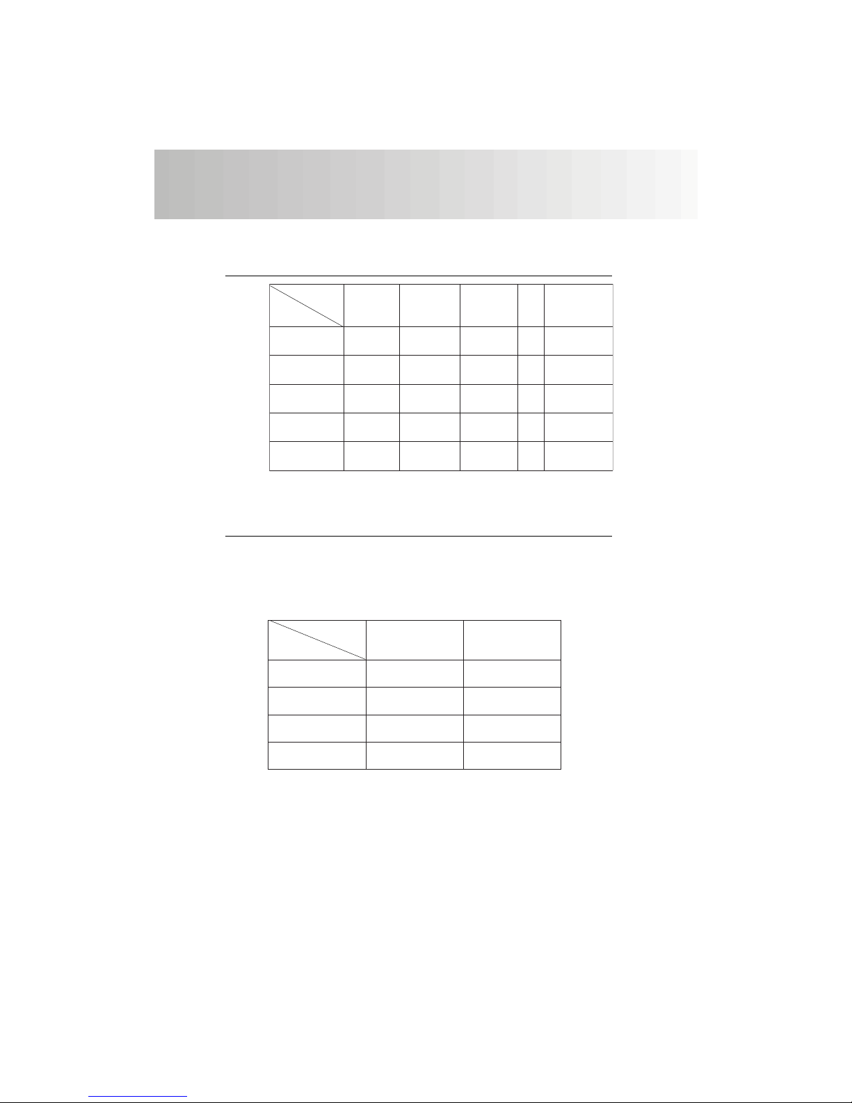
1-1WS2-1WS3-1WS1-2WS
zHM081FFONOFFOFFO
zHM002FFONOFFONO
zHM332FFOFFONONO
zHM662NOFFONOFFO
zHM003NONOFFOFFO
SW
CPU
Any CPU setting change is strongly prohibited!!
DOC Address Select SW1 (5, 6)
The DiskOnChip 2000 occupies an 8 K byte window in the upper
memory address range of D400 to E000. Y ou should ensure this does
not conflict with any other device's memory address.
The configuration are as follows:
These addresses might conflict with the ROM BIOS of other peripheral boards. Please select the appropriate memory address to avoid
memory conflicts.
56
elbasiDNONO
004DFFOFFO
008DNOFFO
00CDFFONO
SW1
Address
Page 12

PCM-4896L
12 PCM-4896L Installation Guide
BC-599/596
 Loading...