

Page 1
User Manual
PCA-6782
Intel® Atom™ Dual-Core D525/
Fanless N455 CPU, ISA Half-size
SBC with VGA / LVDS / Single-GbE /
SATA / COM
Page 2

PCA-6782 User Manual ii
Copyright
The documentation and the software included with this product are copyrighted 2010
by WKHPDQXIDFWXUHU. All rights are reserve
d. 7KHPDQXIDFWXUHU reserves the right
to make improvemen
ts in the products described in this manual at any time without
notice.
No part of this manual may be reproduced, copied, translated or transmitted in any
form or by any means without the prior written permission of WKHPDQXIDFWXUHU.
Information provided in this manual is intended to be accurate and reliable. However,
WKHPDQXIDFWXUHU assumes no responsibility for its use, nor for any infringements
of
the rights of third parties, which may result from its use.
Certifications
CE
FCC Class A
Part No. 2002678200 Edition 1
December 2010
Page 3

PCA-6782 User Manual iv
Product Warranty (2 years)
7KHPDQXIDFWXUHU warrants to you, the original purchaser, that each of its products will be
free
from defects in materials and workmanship for two years from the date of pur-
chase.
This warranty does not apply to any products which have been repaired or altered by
persons other than repair personnel authorized by
WKHPDQXIDFWXUHU, or which have been
subje
ct to misuse, abuse, accident or improper installation.
7KHPDQXIDFWXUHU assumes no
liability und
er the terms of this warranty as a consequence of such events.
Because of
WKHPDQXIDFWXUHU’s high quality-control standards and rigorous testing, most of
ou
r customers never need to use our repair service. If a
product is defecWLYH
it will be repaired or replaced at no charge during the warranty period. For outof-warr
anty repairs, you will be billed according to the cost of replacement materials,
service time and freight. Please consult your dealer for more details.
If you think you have a defective product, follow these steps:
1. Collect all the information about the problem encountered. (For example, CPU
speed,
other hardware and software used, etc.) Note DQ\WKLQJDEQRUPDODQG
list any onscreen messages you get when the problem RFFXUV
2. Call your dealer and describe the problem. Please have your manual, product,
and any helpful information readily available.
3. If your product is diagnosed as defective, obtain an RMA (return merchandise
authorization) number from your dealer. This allows us to process your return
more quickly.
4. Carefully pack the defective product, a fully-completed Repair and Replacement
Order Card and a photocopy proof of purchase date (such as your sales receipt)
in a shippable container. A product returned without proof of the purchase date
is not eligible for warranty service.
5. Write the RMA number visibly on the outside of the package and ship it prepaid
to your dealer.
Before you begin installing your single board computer, please make sure that the
following materials have been shipped:
If any of these items are missing or damaged, contact your distributor or sales representative immediately.
We have carefully inspected the PCA-6782 mechanically and electrically before shipment. It should be free of marks and scratches and in perfect working order upon
receipt.
As you unpack the PCA-6782, check it for signs of shipping damage. (For example,
damaged box, scratches, dents, etc.) If it is damaged or it fails to meet the specifications, notify our service department or your local sales representative immediately.
Also notify the carrier. Retain the shipping carton and packing material for inspection
by the carrier. After inspection, we will make arrangements to repair or replace the
unit.
Page 4

v PCA-6782 User Manual
Initial Inspection
Before you begin installing your single board computer, please make sure that the
following materials have been shipped:
If any of these items are missing or damaged, contact your distributor or sales representative immediately.
We have carefully inspected the PCA-6782 mechanically and electrically before shipment. It should be free of marks and scratches and in perfect working order upon
receipt.
As you unpack the PCA-6782, check it for signs of shipping damage. (For example,
damaged box, scratches, dents, etc.) If it is damaged or it fails to meet the specifications, notify our service department or your local sales representative immediately.
Also notify the carrier. Retain the shipping carton and packing material for inspection
by the carrier. After inspection, we will make arrangements to repair or replace the
unit.
! 1 PCA-6782D(N) single board computer
! 1 CPU Cooler for Atom D525 CPU (Only Available for D SKU) P/N: 1960046526N001
! 1 PCA-6782 Startup Manual
! 1 CD with driver utility and manual (in PDF format)
! 1 Ultra ATA 66/100 HDD cables P/N: 1701400452
! 2 Serial ATA HDD data cable P/N: 1700003194
! 2 Serial ATA HDD power cable P/N: 1703150102
! 1 Print port & COM part cable kit P/N: 1700008954
! 1 ATX Feature Cable P/N: 1700002343
! 1 4-Port USB cable kit P/N: 1700014398
! 1 Y cable for PS/2 keyboard and PS/2 mouse P/N: 1700060202
! 1 ATX power cable 20P/7P 10cm P/N: 1703070101
! 1 AT Power Cable P/N: 1703080101
! 1 Jumper Pack P/N: 9689000002
! 1 Warranty card
Note! Using PCA-6782D's proprietary CPU cooler included in its package is a
must. Other brands of CPU coolers are NOT compatible with PCA-6782.
PCA-6782N is a fanless CPU type and does not require installing a CPU
cooler.
Page 5

PCA-6782 User Manual vi
Verified Memory List
Brand Size Speed Type ECC Vendor PN
PN
Memory
Transcend
256 MBDDR2
667
SODIMM
DDR2
N TS32MSQ64V6M NA
Hynix HY5PS121621B FP-Y5
(32x16)
512 MBDDR2
667
SODIMM
DDR2
N
TS6QSJ23002-6S/
TS64MSQ64V6J
96SD2512M667NNTR
SAMSUNG K4T51083QC ZCE6
(64x8)
512 MBDDR2
667
SODIMM
DDR2
N
Hynix
HY5PS121621B
FP-Y5
NA
Hynix HY5PS121621B FP-Y5
(32x16)
1 GB
DDR2
667
SODIMM
DDR2
N TS128MSQ64V6J NA
SAMSUNG K4T51083QC ZCE6
(64x8)
2 GB
DDR2
667
SODIMM
DDR2
N TS5QSU27300-6M
96SD22G667NN-TR
Micron D9HNL (128x8)
Apacer
512 MBDDR2
667
SODIMM
DDR2
N 78.92G63.422 NA ELPIDA E5108AG-6E-E (64x8)
1 GB
DDR2
667
SODIMM
DDR2
N 78.02G63.423
96SD21G667NN-AP
ELPIDA E5108AGBG-6E-E
(64x8)
2 GB
DDR2
667
SODIMM
DDR2
N 78.A2G72.425
96SD22G667NNAP1
ELPIDA E1108AFBG-8E-F
(128x8)
DSL
256 MBDDR2
667
SODIMM
DDR2
N NA NA ELPIDA E5116AF-6E-E (32x16)
512 MBDDR2
667
SODIMM
DDR2
NNA NA
ELPIDA E5108AGBG-6E-E
(64x8)
1 GB
DDR2
667
SODIMM
DDR2
NNA NA
ELPIDA E5108AGBG-6E-E
(64x8)
2 GB
DDR2
667
SODIMM
DDR2
NNA NA
ELPIDA E1108ACSE-6E-E
(128x8)
Page 6

vii PCA-6782 User Manual
Certification and Safety Instructions
This device complies with the requirements in part 15 of the FCC rules: Operation is
subject to the following two conditions:
1. This device may not cause harmful interference, and
2. This device must accept any interference received, including interference that
may cause undesired operation
This equipment has been tested and found to comply with the limits for a Class A digital device, pursuant to Part 15 of the FCC Rules. These limits are designed to provide reasonable protection against harmful interference when the equipment is
operated in a commercial environment. This equipment generates, uses, and can
radiate radio frequency energy and, if not installed and used in accordance with the
instruction manual, may cause harmful interference to radio communications. Operation of this device in a residential area is likely to cause harmful interference in which
case the user will be required to correct the interference at his/her own expense. The
user is advised that any equipment changes or modifications not expressly approved
by the party responsible for compliance would void the compliance to FCC regulations and therefore, the user's authority to operate the equipment.
Caution! There is a danger of a new battery exploding if it is incorrectly installed.
Do not attempt to recharge, force open, or heat the battery. Replace the
battery only with the same or equivalent type recommended by the manufacturer. Discard used batteries according to the manufacturer's
instructions.
Page 7

PCA-6782 User Manual viii
Page 8

ix PCA-6782 User Manual
Contents
Chapter 1 Hardware Configuration......................1
1.1 Introduction ............................................................................................... 2
1.2 Features .................................................................................................... 2
1.3 Specifications ............................................................................................ 3
1.3.1 System .......................................................................................... 3
1.3.2 Memory ......................................................................................... 3
1.3.3 Input/Output .................................................................................. 3
1.3.4 Graphic interface........................................................................... 3
1.3.5 Ethernet LAN ................................................................................ 4
1.3.6 Industrial features ......................................................................... 4
1.3.7 Mechanical and environmental specifications............................... 4
1.4 Jumpers and Connectors .......................................................................... 5
Table 1.1: Jumper descriptions ................................................... 5
Table 1.2: Connector descriptions............................................... 5
1.5 Board Layout: Jumper and Connector Locations...................................... 7
Figure 1.1 Board Layout .............................................................. 7
1.6 PCA-6782 Block Diagram ......................................................................... 8
Figure 1.2 Block Diagram ............................................................ 8
1.7 Safety Precautions .................................................................................... 8
1.8 System Memory ........................................................................................ 9
1.9 Memory Installation Procedures................................................................ 9
1.10 Processor Installation.............................................................................. 10
1.11 CPU Cooler Installation........................................................................... 10
Chapter 2 Connecting Peripherals & Jumper
Settings ..............................................11
2.1 Introduction ............................................................................................. 12
2.2 IDE Connector (IDE1) ............................................................................. 12
Figure 2.1 PCA-6782 IDE1 location........................................... 12
2.3 Floppy Drive Connector (FDD1).............................................................. 13
Figure 2.2 PCA-6782 FDD1 location ......................................... 13
2.4 Parallel Port (LPT1)................................................................................. 14
Figure 2.3 PCA-6782 LPT1 location .......................................... 14
2.5 VGA Connector (VGA1) .......................................................................... 15
Figure 2.4 VGA Connector (VGA1) ........................................... 15
2.6 Serial Ports (COM1, COM2) ................................................................... 15
Figure 2.5 Serial Ports (COM1, COM2) ..................................... 15
2.7 PS/2 Keyboard/Mouse Connector (KBMS1) ........................................... 16
Figure 2.6 PS/2 Keyboard/Mouse Connector (KBMS1) ........... 16
2.8 External Keyboard Pin Header (KBMS2) ................................................ 17
Figure 2.7 External Keyboard Connector (KBMS2) .................. 17
2.9 CPU Fan Connectors (CPUFAN1).......................................................... 17
Figure 2.8 CPU Fan Connectors (CPUFAN1) .......................... 17
2.10 Front Panel Connectors (JFP1) ............................................................. 18
Figure 2.9 Front Panel Connectors (JFP1) ............................... 18
2.10.1 ATX Power Button (JFP1 Pin 9~10) ........................................... 18
2.10.2 Reset (JFP1 Pin 7~8) ................................................................. 18
2.10.3 Suspend LED (JFP1 Pin 5~6)..................................................... 18
2.10.4 Power LED and keyboard lock connector (JFP1 Pin 3~4).......... 18
Table 2.1: ATX power supply LED status (No support for AT pow-
er) ............................................................................. 18
2.10.5 HDD LED (JFP1 Pin 1~2) ........................................................... 19
Page 9

PCA-6782 User Manual x
2.11 Watch Dog Timer (JWDT1) / Infrared (JIR1) .......................................... 19
Figure 2.10Watch Dog Timer (JWDT1) / Infrared (JIR1) ............ 19
2.11.1 Watchdog timer output (JWDT1) ................................................ 19
Table 2.2: Watchdog timer output (JWDT1).............................. 19
2.11.2 Infrared Connector (JIR1)........................................................... 19
2.12 Single Giga LAN RJ45 connector (LAN1)............................................... 20
Figure 2.11Single Giga LAN RJ45 connector (LAN1) ................ 20
2.13 Serial ATA interface (SATA1 ~ SATA3).................................................. 20
Figure 2.12Serial ATA interface (SATA1 ~ SATA3) ................... 20
2.14 GPIO header (GPIO1) ............................................................................ 21
Figure 2.13 GPIO header (GPIO1)............................................. 21
2.15 LVDS panel power selection (JLVDS1) .................................................. 21
Table 2.3: LVDS panel power selection (JLVDS1).................... 21
2.16 LVDS VBR selection (JVBR1) ................................................................ 22
Table 2.4: LVDS VBR selection (JVBR1).................................. 22
2.17 CMOS clear (CMOS1) ............................................................................ 22
Table 2.5: CMOS (CMOS1) ...................................................... 22
2.18 ATX Feature connector(ATXF1) ............................................................. 23
2.19 ATX power control connector (ATX1) ..................................................... 24
2.20 System FAN connector (SYSFAN1) ....................................................... 24
2.21 LVDS Signal and Power Connectors (LVDS1) ....................................... 25
2.22 USB Ports (USB 1 ~ 8) ........................................................................... 25
2.23 CF Card Socket ...................................................................................... 26
2.24 Low Pin Count Device Connection Pin Header ...................................... 26
Chapter 3 AMI BIOS Setup................................. 27
Figure 3.1 Setup Program Initial Screen ................................... 28
3.1 Entering Setup ........................................................................................ 29
3.2 Main Setup.............................................................................................. 29
Figure 3.2 Main Setup Screen ................................................... 29
3.2.1 System time / System date ......................................................... 29
3.3 Advanced BIOS Features Setup............................................................. 30
Figure 3.3 Advanced BIOS Features Setup Screen .................. 30
3.3.1 CPU Configuration...................................................................... 31
Figure 3.4 CPU Configuration Settings ..................................... 31
3.3.2 IDE Configuration ....................................................................... 32
Figure 3.5 IDE Configuration ..................................................... 32
3.3.3 Super I/O Configuration .............................................................. 33
Figure 3.6 Super I/O Configuration............................................ 33
3.3.4 Hardware Health Function .......................................................... 34
Figure 3.7 Hardware Health Configuration. ............................... 34
3.3.5 APM Configuration...................................................................... 35
Figure 3.8 APM Configuration ................................................... 35
3.4 Event Logging Details ............................................................................. 36
Figure 3.9 Event Logging Details .............................................. 36
3.5 USB Configuration .................................................................................. 36
Figure 3.10USB Configuration.................................................... 36
3.6 PCI/PNP Setup ....................................................................................... 37
Figure 3.11PCI/PNP Setup......................................................... 37
3.7 Boot Setup Utility .................................................................................... 38
Figure 3.12Boot Settings Configuration...................................... 38
3.8 Security Setup......................................................................................... 39
Figure 3.13Password Configuration ........................................... 39
3.9 Advanced Chipset Settings..................................................................... 40
Figure 3.14Advanced Chipset Settings ...................................... 40
Figure 3.15South Bridge Configuration ...................................... 42
3.10 Exit Options............................................................................................. 43
Figure 3.16Exit Options .............................................................. 43
Page 10

xi PCA-6782 User Manual
3.10.1 Save Changes and Exit .............................................................. 43
3.10.2 Discard Changes and Exit .......................................................... 43
3.10.3 Discard Changes ........................................................................ 43
3.10.4 Load Optimal Defaults ................................................................ 44
3.10.5 Load Failsafe Defaults ................................................................ 44
Chapter 4 Value-Added Software Services.......45
4.1 Value-Added Software Services ............................................................. 46
4.1.1 Software API ............................................................................... 46
4.1.2 Software Utility ............................................................................ 48
Chapter 5 Chipset Software Installation Utility 49
5.1 Before You Begin .................................................................................... 50
5.2 Introduction ............................................................................................. 50
5.3 Windows 7/XP Driver Setup.................................................................... 51
Chapter 6 Integrated Graphic Device Setup .....53
6.1 Introduction ............................................................................................. 54
6.2 Windows 7/XP Driver Setup.................................................................... 54
Chapter 7 LAN Configuration.............................55
7.1 Introduction ............................................................................................. 56
7.2 Installation ............................................................................................... 56
7.3 Windows 7/XP Driver Setup.................................................................... 56
Appendix A Programming the Watchdog Timer..57
A.1 Watchdog Timer...................................................................................... 58
A.1.1 Watchdog Timer Overview.......................................................... 58
A.1.2 Reset/ Interrupt Selection ........................................................... 58
A.1.3 Programming the Watchdog Timer ............................................. 59
Table A.1: Watchdog Timer Registers ....................................... 60
A.1.4 Example Program ....................................................................... 61
Appendix B I/O Pin Assignments..........................65
B.1 Front Panel Connectors (JFP1) .............................................................. 66
Table B.1: Front Panel Connectors (JFP1)................................ 66
B.2 USB Ports (USB12/USB34/USB56/USB78) ........................................... 66
Table B.2: USB Ports (USB12/USB34/USB56/USB78)............. 66
B.3 IR Connector (JIR1) ................................................................................ 67
Table B.3: IR Connector (JIR1).................................................. 67
B.4 Serial port (COM1) .................................................................................. 67
Table B.4: Serial port (COM1)................................................... 67
B.5 Serial port (COM2) .................................................................................. 68
Table B.5: Serial port (COM2) ................................................... 68
B.6 PS/2 keyboard and mouse connector (KBMS1) ..................................... 68
Table B.6: PS/2 keyboard and mouse connector (KBMS1)....... 68
B.7 External keyboard and mouse connector (KBMS2) ................................ 69
Table B.7: External keyboard and mouse connector (KBMS2) . 69
B.8 ATX Feature connector(ATXF1) ............................................................. 69
Page 11

PCA-6782 User Manual xii
Table B.8: ATX Feature connector(ATXF1)............................... 69
B.9 CPU FAN connector (CPUFAN1) ........................................................... 70
Table B.9: CPU FAN connector (CPUFAN1)............................. 70
B.10 System FAN connector (SYSFAN1) ....................................................... 70
Table B.10:System FAN connector (SYSFAN1)......................... 70
B.11 Audio Interface Connector (HDAUD1) .................................................... 70
Table B.11:Audio Interface Connector (HDAUD1) ..................... 70
B.12 GPIO Header (GPIO1)............................................................................ 71
Table B.12:GPIO Header (GPIO1) ............................................. 71
B.13 LVDS Connector (LVDS1) ...................................................................... 71
Table B.13:LVDS Connector (LVDS1)........................................ 71
B.14 LCD Inverter Connector (INV1)............................................................... 72
Table B.14:LCD Inverter Connector (INV1) ................................ 72
B.15 Low Pin Count Header (LPC1) ............................................................... 72
Table B.15:Low Pin Count Header (LPC1)................................. 72
B.16 ATX Power Control Connector (ATX1) ................................................... 73
Table B.16:ATX Power Control Connector (ATX1)..................... 73
B.17 VGA Connector (VGA1).......................................................................... 73
Table B.17:VGA Connector (VGA1) ........................................... 73
B.18 Negative power input connector (12V1).................................................. 74
Table B.18:Negative power input connector (12V1) ................... 74
B.19 Case open (JCASE1).............................................................................. 74
Table B.19:Case open (JCASE1) ............................................... 74
B.20 FDD connector (FDD1) ........................................................................... 75
Table B.20:FDD connector (FDD1) ............................................ 75
B.21 Parallel port connector (LPT1) ................................................................ 76
Table B.21:Parallel port connector (LPT1) ................................. 76
B.22 IDE connector (IDE1).............................................................................. 77
Table B.22:IDE connector (IDE1) ............................................... 77
B.23 Serial ATA (SATA1/SATA2/SATA3) ....................................................... 78
Table B.23:Serial ATA (SATA1/SATA2/SATA3)......................... 78
B.24 HW Monitor Alarm (JOBS1).................................................................... 78
Table B.24:Serial ATA (SATA1/SATA2/SATA3)......................... 78
B.25 LVDS VBR selection (JVBR1) ................................................................ 79
Table B.25:LVDS VBR selection (JVBR1).................................. 79
B.26 LVDS panel power selection (JLVDS1) .................................................. 79
Table B.26:LVDS panel power selection (JLVDS1).................... 79
B.27 Watchdog timer output selection (JWDT1) ............................................. 79
Table B.27:Watchdog timer output selection (JWDT1)............... 79
B.28 CMOS clear (CMOS1) ............................................................................ 80
Table B.28:CMOS clear (CMOS1).............................................. 80
B.29 System I/O Ports..................................................................................... 80
Table B.29:System I/O ports....................................................... 80
B.30 DMA Channel Assignments .................................................................... 81
Table B.30:DMA channel assignments....................................... 81
B.31 Interrupt Assignments ............................................................................. 81
Table B.31:Interrupt assignments............................................... 81
B.32 1st MB Memory Map............................................................................... 82
Table B.32:1st MB memory map ................................................ 82
Appendix C Programming the GPIO .................... 83
C.1 Supported GPIO Register ....................................................................... 84
C.1.1 GPIO Registers........................................................................... 84
C.1.2 GPIO Example Program-1.......................................................... 85
Page 12

Chapter 1
1 Hardware
Configuration
Page 13

PCA-6782 User Manual 2
1.1 Introduction
PCA-6782 is an Intel® Atom™ dual-core D525 / fanless N455 CPU based ISA-interface half-size single board computer. With high performance Atom D525 dual-core
computing power, it is ideal for intense data or graphic processing applications; with
fanless Atom™ N455 CPU, it has ultra high reliability to resist heat, dust, vibration
and shock in any application environment.
PCA-6782 is designed with an Intel
®
Atom™ D525/N455 CPU and ICH8M I/O control
hub. The Atom™ D525 dual core CPU brings new generation computing capability
into the half-size SBC application field. Compact size, low power consumption (Total
power consumption ≤ 17.62 W) and dual-core parallel computing power and maxi-
mum 2 GB of DDR2 667 MHz memory capacity makes the PCA-6782D a powerful
small form-factor computer platform for modern industrial applications that require
high computing power. The fanless Atom™ N455 CPU (Total power consumption ≤
12.56 W) is ideal for data-acquisition, environment monitoring system and factory
automation that requires no air flow environments.
PCA-6782 has an integrated graphic core of Intel Embedded Gen3.5+ graphic technology with 224 MB shared memory. This feature makes PCA-6782 is capable of
handling complex and intense 2D/3D graphic processing without an add-on graphic
card; its VGA and LVDS dual video outputs also makes it suitable for applications
requiring dual display or digital panel display capabilities.
PCA-6782 is rich in I/O interfaces: it has three SATA ports (300 MB/sec) for mainstream SSD (solid state disk), HDD, and ODD connections, one legacy IDE port for
the ODD connection. It also has a CF socket to support an economical, easy-tomaintain SSD device. Additionally, the two serial ports (COM ports) can be used as
reliable legacy device control interfaces. Users can also purchase
WKH COMSRUW
upgrade module (P/N: PCA-COM485-00A1E) to have four extra RS485 ports
with
auto flow control capability.
1.2 Features
! Ultra low power (Total Power Consumption ≤ 12.56 W), fanless N455 CPU and
maximum 2 GB DDR2 667 memory (Only for N SKU)
! Dual-core D525 CPU and maximum 2 GB DDR2 667 memory (Only for D SKU)
! Intel® Embedded Gen3.5+ graphics core with 224 MB of shared memory with
VGA/LVDS dual video outputs (supporting clone and extension modes)
! Supports single-Gigabit Ethernet LANs with teaming capability
! Supports Embedded Software SUSI APIs and Utilities. (SUSI APIs: watchdog,
hardware monitor, brightness control, programmable GPIO, backlight On/Off;
Utilities: BIOS flash, eSOS (Requires BIOS Customization), system monitoring,
Flash Lock, software protection)
Page 14

3 PCA-6782 User Manual
Chapter 1 Hardware Configuration
1.3 Specifications
1.3.1 System
! CPU: Soldered-down (BGA type) Intel® Atom™ 1.8 GHz D525 dual-core CPU
or 1.66GHz N455 fanless CPU
! L2 Cache: CPU built-in 1 MB / 512 KB L2 cache
! BIOS: AMI BIOS
! System Chipset: Intel
®
ICH8M
! SATA/EIDE hard disk drive interface: Supports up to 3 independent Serial
ATA hard drives (up to 300 MB/s) as well as one IDE port (maximum 2 devices)
! Floppy disk drive interface: Supports up to two floppy disk drives, 5
1
/4 (360
KB and 1.2 MB) and/or 3
1
/2 (720 KB, 1.44 MB). BIOS enabled/disabled.
1.3.2 Memory
! RAM:
– N and D SKU: Maximum 2 GB DDR2 667 MHz memory in SO-DIMM socket
1.3.3 Input/Output
! Enhanced parallel port: Configurable to LPT1 or disabled. Standard DB-25
female connector provided. Supports EPP/ECP
! Serial ports: Two dedicated serial RS-232 ports on board, plus four ports RS-
422/485 w/ autoflow control by module (Optional,
P/N: PCA-&20$(
! Keyboard and PS/2 mouse connector: One 6-pin mini-DIN connector is
located on the mounting bracket for easy connection to a keyboard or PS/2
mouse. An on board keyboard pin header connector is also available
! High Definition Audio: PCA-6782 can provide audio function with the optional
audio extension module PCA-AUDIO-HDA1E
! USB ports: PCA-6782 supports up to 8 USB 2.0 ports with transmission rates
up to 480 Mbps
1.3.4 Graphic interface
! Controller: Integrated graphics core of Embedded Gen3.5+ technology
! VRAM: 224 MB shared system memory
! Output Interfaces:
– VGA: Supports up to SXGA 1400 x 1050 @ 60Hz for Atom N455, up to 2048
x 1536 @ 60 Hz for Atom D525
– LVDS: Supports 18-bit single channel and up to WXGA 1366 x 768 or 1280 x
800 for both Atom D525 and N455 CPUs
– Dual Display: VGA + LVDS, supports extended mode and clone mode
Note! PCA-6782 is ONLY compatible with DDR2 memory modules that are
assembled with x16 (16-bit) memory chips and NOT compatible with
those that are assembled with x8 (8-bit) memory chips. Using wrong
memory modules may cause unexpected system instability.
Page 15

PCA-6782 User Manual 4
1.3.5 Ethernet LAN
! Supports single 10/100/1000 Mbps Ethernet networking
! Controller: Intel
®
82567V
1.3.6 Industrial features
! Watchdog timer: Can generate a system reset. The watchdog timer is pro-
grammable, with each unit equal to one second or one minute (255 levels). You
can find programming details in Appendix A
! Fanless N455 CPU for N SKU for ultra high reliability and long MTBF
1.3.7 Mechanical and environmental specifications
! Operating temperature: 0 ~ 60° C (32 ~ 140° F)
! Storage temperature: -40 ~ 85° C (-40 ~ 185° F)
! Humidity: 20 ~ 95% non-condensing
! Demanded Power supply voltage: +12 V, +5 V, +5 VSB
! Power consumption:
– D SKU:
CPU: Dual-core Atom D525 CPU 1.8 GHz
Memory: 1 Piece of 2 GB DDR2 667 MHz SO-DIMM
Storage: One SATA HDD
Test program: Hot CPU pro 4.22
+12 V: 0.46 A
+5 V: 2.41 A
+3.3 V: 0 A
+5 VSB: 0.01 A
-12 V: 0 A
-5 V: 0 A
Total Power Consumption: 17.62 W
– N SKU:
CPU: Single Core Atom N455 CPU 1.66 GHz
Memory: 1 Piece of 2 GB DDR2 667 MHz SO-DIMM
Storage: One STA HDD
Test Progr a m: Hot CPU pro 4.22
+12 V: 0.13 A
+5 V: 2.19 A
+3.3 V: 0 A
+5 VSB: 0.01 A
-12 V: 0 A
-5 V: 0 A
Total Power Consumption: 12.56 W
! Board size: 185 mm (L) x 122 mm (W) (7.3" x 4.8")
! Board weight: 0.225 Kg (weight of board)
Page 16

5 PCA-6782 User Manual
Chapter 1 Hardware Configuration
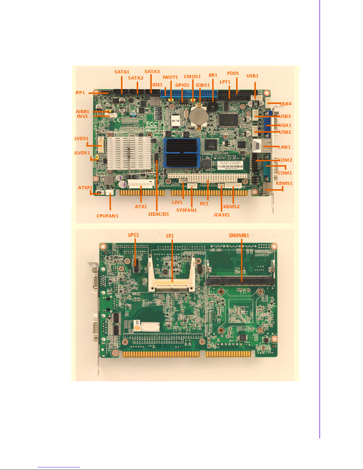
1.4 Jumpers and Connectors
Connectors on the PCA-6782 single board computer link it to external devices such
as hard disk drives and a keyboard. In addition, the board has a number of jumpers
used to configure your system for your application.
Below, Tables 1.1 and 1.2 list the jumper and connector functions. Later sections in
this chapter give instructions on setting jumpers. Chapter 2 gives instructions for connecting external devices to your single board computer.
Table 1.1: Jumper descriptions
Label Function
CMOS1 CMOS Clear
JWDT1 Watchdog timer output option
JLV DS 1 LVDS pa ne l pow er s elec ti on
JVBR1 LVDS VBR s election
Table 1.2: Connector descriptions
Label Function
IDE1 Primary IDE connector
FDD1 Floppy drive connector
LPT1 Parallel port
VGA1 VGA connector
LVDS1 LVDS Pin-header
COM1 Serial port: COM1; RS232 (9-pin D-sub)
COM2 Serial port: COM2; RS-232 (14-pin 2.00 pitch box header)
KBMS1 PS/2 keyboard and mouse connector
KBMS2 External keyboard/mouse pin header
JIR1 Infrared port pin header
CPUFAN1 3-pin Atom D525 CPU fan connector
SYSFAN1 3-pin System fan connector
JFP1 Power and Reset Button connector
LAN1 Single Giga LAN RJ45 connector with Transformer
HDAUD1 High Definition Audio interface connector
SATA1 Serial ATA1
SATA2 Serial ATA2
SATA3 Serial ATA3
USB 12 USB port 1 and port 2 pin-header
USB 34 USB port 3 and port 4 pin-header
USB 56 USB port 5 and port 6 pin-header
USB 78 USB port 7 and port 8 pin-header
GPIO1 GPIO header
JOBS1
HW Monitor Alarm
Close: Enable OBS Alarm
Open: Disable OBS Alarm
PC1 PC104 connector
JCASE1 Case open
DIMMB1 Memory connector channel B
Page 17

PCA-6782 User Manual 6
INV1 LCD inverter connector
CF1 CF Socket
ATXF1 ATX feature connector
ATX1 ATX power connector
12V1 Negative power input connector
LPC1 Low pin count connector
Table 1.2: Connector descriptions
Page 18
7 PCA-6782 User Manual
Chapter 1 Hardware Configuration
1.5 Board Layout: Jumper and Connector
Locations
Figure 1.1 Board Layout
Page 19
PCA-6782 User Manual 8
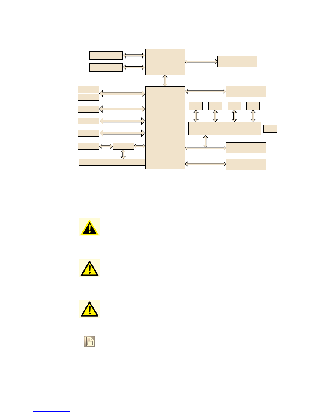
1.6 PCA-6782 Block Diagram
Figure 1.2 Block Diagram
1.7 Safety Precautions
Atom D525
Atom N455
CPU
CRT
LVDS 18bit
IDE
CFC
3 SATA
8 USB
BIOS
PC104 ITE8888G
ISA Golden Finger
ICH8M
SODIMM DDR2 667
Socket to 2 G Max
G-LAN1: Intel 82567V
2 COM
8-bit GPIO
Super IO
W83627DHG-P
4 COM With Auto
flow Control (Optional)
ALC 888 Codec
PCA-AUDIO-HDA1E (Optional)
FDD PS2 LPT
Single channel
x4 DMI
VGA
LVDS
IDE
300 MB/s
USB 2.0
SPI
ISA
LCI & GLCI
Single LAN
LPC Bus
HD Audio
ISA
Warning! Always completely disconnect the power cord from your chassis when-
ever you work with the hardware. Do not make connections while the
power is on. Sensitive electronic components can be damaged by sudden power surges. Only experienced electronics personnel should open
the PC chassis.
Caution! Always ground yourself to remove any static charge before touching the
single board computer. Modern electronic devices are very sensitive to
electrostatic discharges. As a safety precaution, use a grounding wrist
strap at all times. Place all electronic components on a static-dissipative
surface or in a static-shielded bag when they are not in the chassis.
Caution! The computer is provided with a battery-powered real-time clock circuit.
There is a danger of explosion if battery is incorrectly replaced. Replace
only with same or equivalent type recommended by the manufacturer.
Discard used batteries according to manufacturer's instructions.
Note! Before installing your PCA-6782 into a chassis, make sure that no com-
ponents on either side of the CPU card can touch any metal parts, especially the chassis wall and add-on card in the adjacent slot.
Page 20
9 PCA-6782 User Manual
Chapter 1 Hardware Configuration
1.8 System Memory
The PCA-6782D has one SO-DIMM socket. PCA-6782 is ONLY compatible with
DDR2 memory modules that are assembled with x16 (16-bit) memory chips and NOT
compatible with those that are assembled with x8 (8-bit) memory chips. Using wrong
memory modules may cause system instability and unexpected behavior.
1.9 Memory Installation Procedures
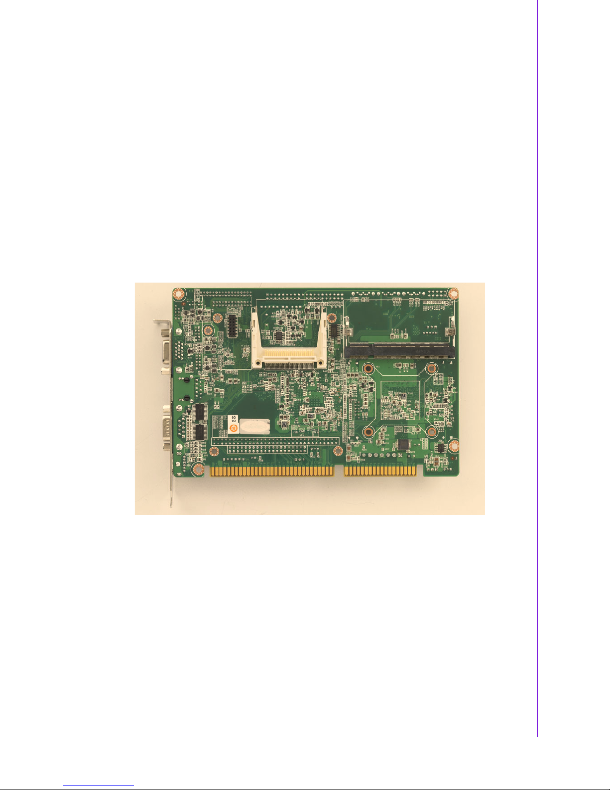
1. See picture below to locate DIMMB1 200-pin SODIMM socket.
2. A memory module and expansion socket are keyed. The plastic bridge in the
socket must align with the notch in the module. The keyed bridge and notch
make sure a SODIMM cannot be installed going the wrong direction.
3. Insert the SODIMM module into the socket at a 30-45 degree angle. Make sure
the notch and the module are properly aligned.
Slowly push down the SODIMM toward the CPU card PCB until the clips at each
end of the expansion socket click into place.
Page 21

PCA-6782 User Manual 10
1.10 Processor Installation
PCA-6782 series are equipped with soldered-down (BGA type) CPUs. no need for a
user to install a CPU.
1.11 CPU Cooler Installation
Only PCA-6782D needs to have a CPU cooler installed by user (P/N:
1960046526N001), PCA-6782N does NOT require this; it already has a passive
heat-sink assembled on the CPU card.
PCA-6782D users please follow the instructions below to install the CPU cooler
which is included in the package.
First locate the Atom D525 CPU then put the metal plate included in CPU cooler
package onto the solder side of the PCB with its four legs inserted into these four
mounting holes around the CPU, then attach the CPU cooler onto the CPU card by
fastening the four screws, one into each leg of the metal plate. Fasten the first screw
loosely, then loosely engage the second screw diagonally across from the first one,
then half fasten the third, and fourth screws. Finally snug all four screws completely,
following the same order.
Warning! Without a fan or heat sink, the CPU will overheat and cause damage to
both itself and the single board computer. If you are a D SKU user,
please install the CPU cooler (P/N: 1960046526N001) before booting up
the system and do NOT remove any on-board passive heat sinks; if you
are an N SKU user, please do NOT remove any on-board passive heat
sinks.
Improper CPU cooler installation may cause serious CPU die damage;
please follow the instructions above to install your CPU cooler.
Page 22

Chapter 2
2 Connecting
Peripherals & Jumper
Settings
Page 23
PCA-6782 User Manual 12
2.1 Introduction
You can access most of the connectors from the top of the board while it is installed
in the chassis. If you have a number of cards installed or have a packed chassis, you
may need to partially remove the card to make all the connections.
You can configure your single board computer to match the needs of your application
by setting the jumpers. A jumper is a metal bridge that closes an electrical circuit. It
consists of two metal pins and a small metal clip (often protected by a plastic cover)
that slides over the pins to connect them. To "close" (or turn ON) a jumper, you connect the pins with the clip. To "open" (or turn OFF) a jumper, you remove the clip.
Sometimes a jumper consists of a set of three pins, labeled 1, 2, and 3. In this case,
you connect either pins 1 and 2, or 2 and 3. A pair of needle-nose pliers may be useful when setting jumpers.
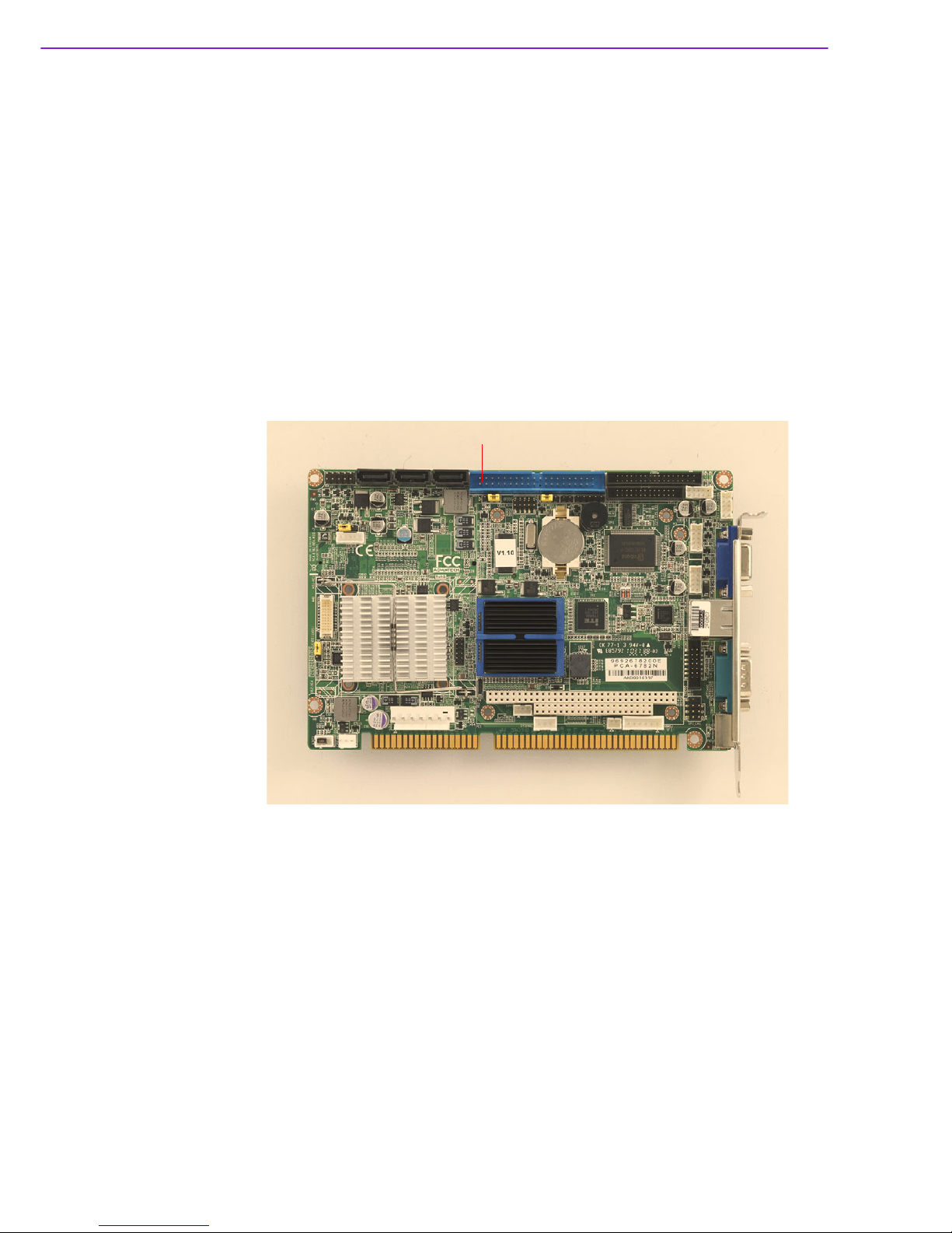
2.2 IDE Connector (IDE1)
Figure 2.1 PCA-6782 IDE1 location
You can attach up to two IDE (Integrated Drive Electronics) drives to the PCA-6782's
built-in controller. The primary connector can accommodate two drives.
Wire number 1 on the cable is red or blue and the other wires are gray. Connect one
end to connector IDE1 on the single board computer. Make sure that the red/blue
wire corresponds to pin 1 on the connector (in the upper right hand corner). See
Chapter 1 for help finding the connector.
Unlike floppy drives, IDE hard drives can connect in either position on the cable. If
you install two drives to a single connector, you will need to set one as the master
and the other as the slave. You do this by setting the jumpers on the drives. If you
use just one drive per connector, you should set each drive as the master. See the
documentation that came with your drive for more information.
Connect the first hard drive to the other end of the cable. Wire 1 on the cable should
also connect to pin 1 on the hard drive connector, which is labeled on the drive circuit
board. Check the documentation that came with the drive for more information.
IDE
Page 24
13 PCA-6782 User Manual
Chapter 2 Connecting Peripherals & Jumper Settings
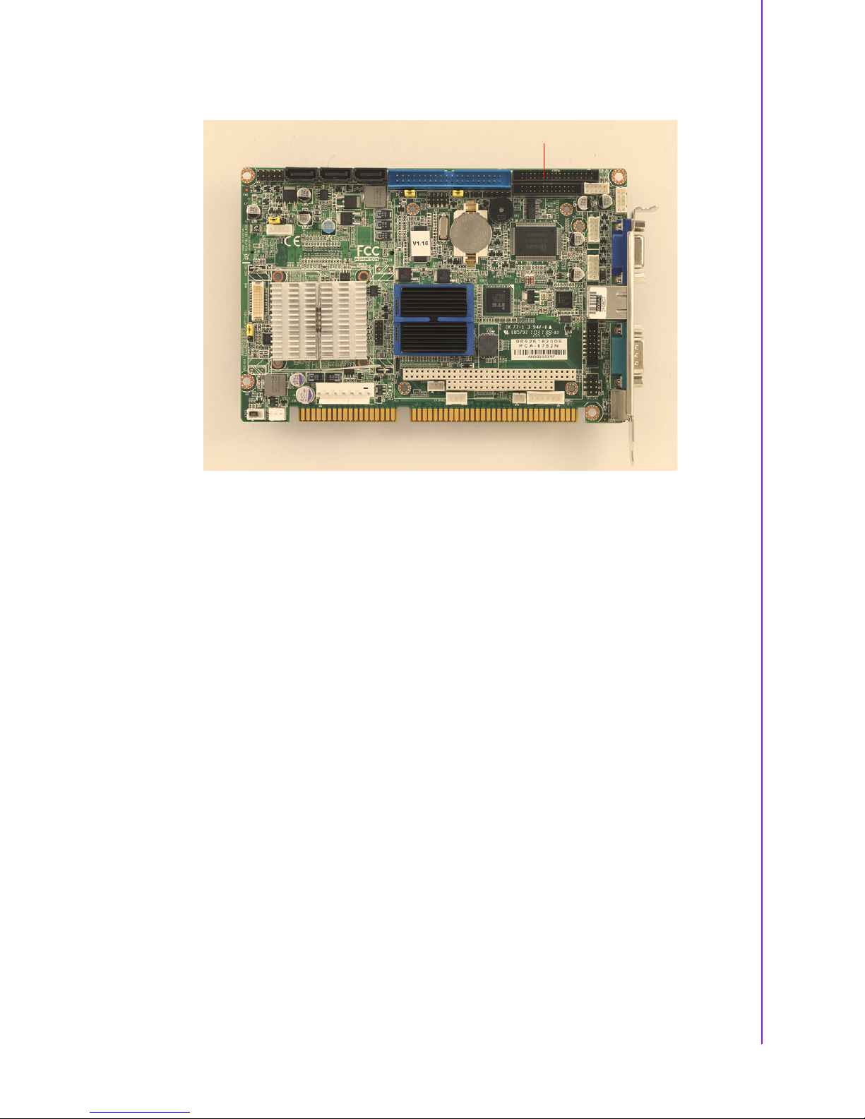
2.3 Floppy Drive Connector (FDD1)
Figure 2.2 PCA-6782 FDD1 location
You can attach one floppy disk drives to the PCA-6782's on board controller. You can
use 3.5" (720 KB, or 1.44 MB) drives.
The single board computer comes with a 34-pin daisy-chain drive connector cable.
On one end of the cable is a 34-pin flat-cable connector. On the other end are two
sets of 34-pin flat-cable connector (usually used for 3.5" drives). The set on the end
(after the twist in the cable) connects to the A: floppy drive. The set in the middle connects to the B: floppy drive.
FDD1
Page 25
PCA-6782 User Manual 14
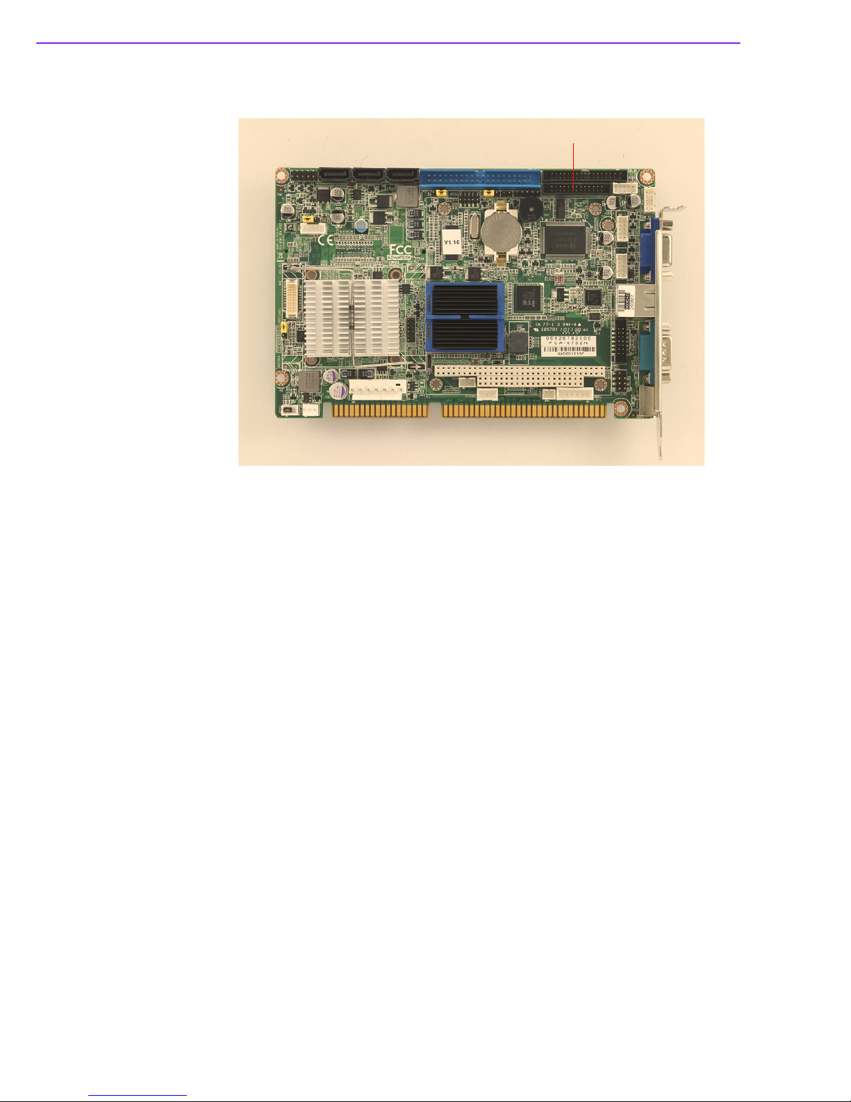
2.4 Parallel Port (LPT1)
Figure 2.3 PCA-6782 LPT1 location
The parallel port is normally used to connect the single board computer to a printer.
The PCA-6782 includes an onboard parallel port, accessed through a 26-pin flatcable connector, LPT1. The card comes with an adapter cable which lets you use a
traditional DB-25 connector. The cable has a 26-pin connector on one end and a DB25 connector on the other, mounted on a retaining bracket. The bracket installs at the
end of an empty slot in your chassis, giving you access to the connector.
The parallel port is designated as LPT1, and can be disabled or changed to LPT2 or
LPT3 in the system BIOS setup.
To install the bracket, find an empty slot in your chassis. Unscrew the plate that covers the end of the slot. Screw in the bracket in place of the plate. Next, attach the flatcable connector to LPT1 on the CPU card. Wire 1 of the cable is red or blue, and the
other wires are gray. Make sure that wire 1 corresponds to pin 1 of LPT1. Pin 1 is on
the upper right side of LPT1.
LPT1
Page 26
15 PCA-6782 User Manual
Chapter 2 Connecting Peripherals & Jumper Settings
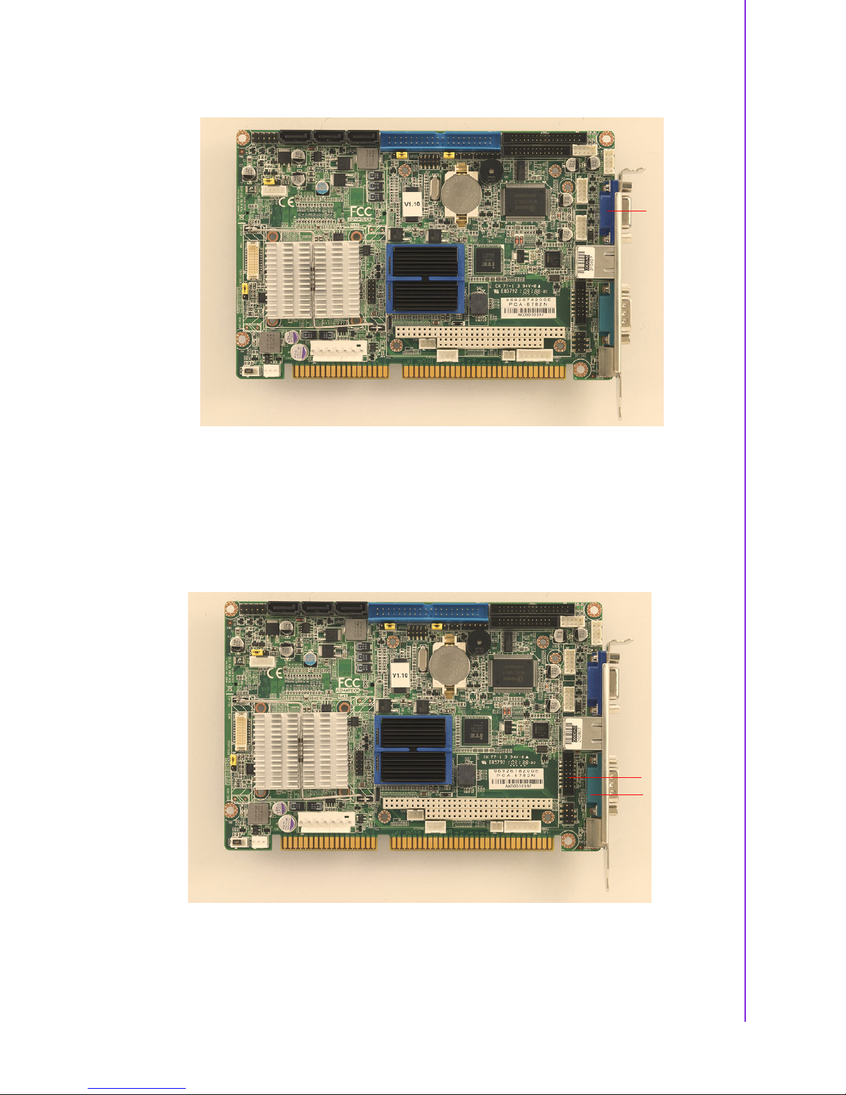
2.5 VGA Connector (VGA1)
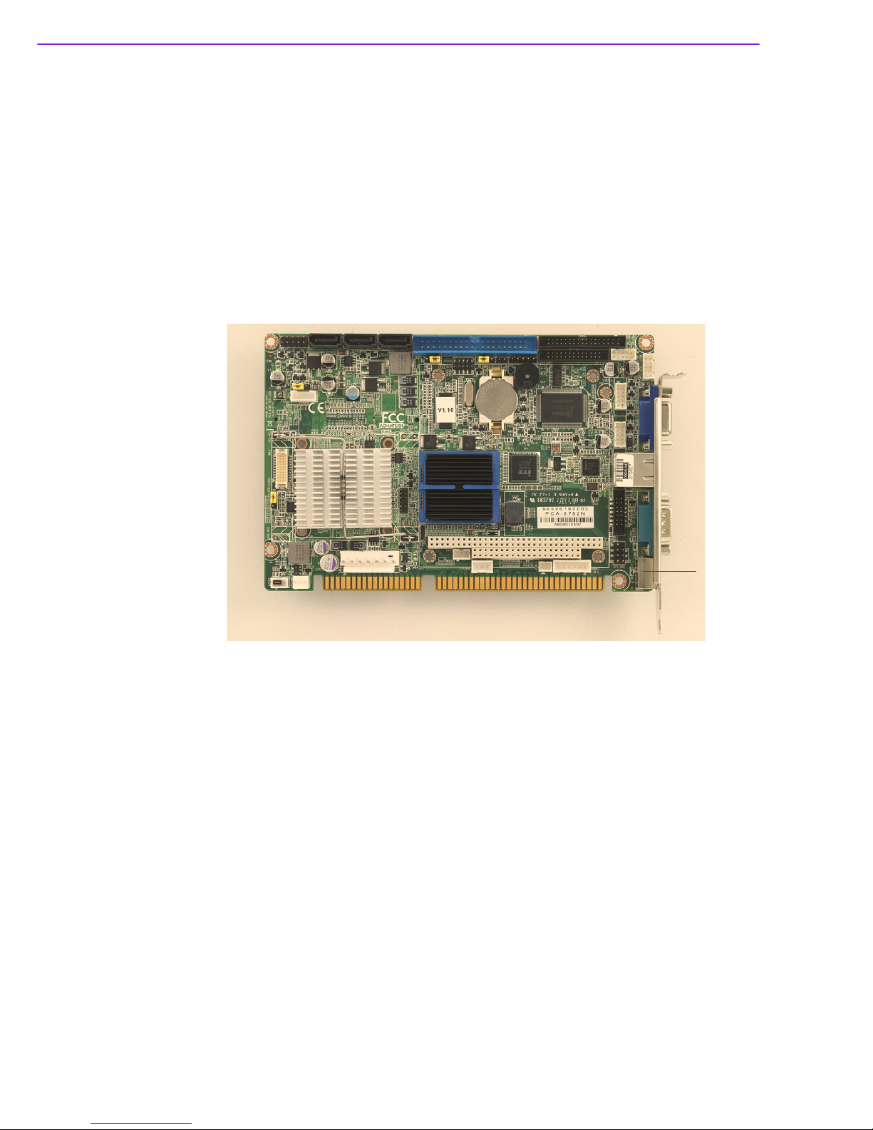
Figure 2.4 VGA Connector (VGA1)
The PCA-6782 includes a VGA interface that can drive conventional CRT displays.
VGA1 is a standard 15-pin D-SUB connector commonly used for VGA. Pin assignments for CRT connector VGA1 are detailed in Appendix B.
2.6 Serial Ports (COM1, COM2)
Figure 2.5 Serial Ports (COM1, COM2)
VGA1
COM2
COM1
Page 27
PCA-6782 User Manual 16
The PCA-6782 offers two serial ports: COM1 and COM2. These ports can connect to
serial devices.
You may connect the dual COM ports cable kit 1700008762 to COM2 box-header to
have these 2 DB9 RS232 ports on the rear bracket.
The IRQ and address ranges for all ports are fixed. However, if you want to disable
the port or change these parameters later, you can do this in the system BIOS setup.
Different devices implement the RS-232 standard in different ways. If you are having
problems with a serial device, be sure to check the pin assignments for the connector.
2.7 PS/2 Keyboard/Mouse Connector (KBMS1)
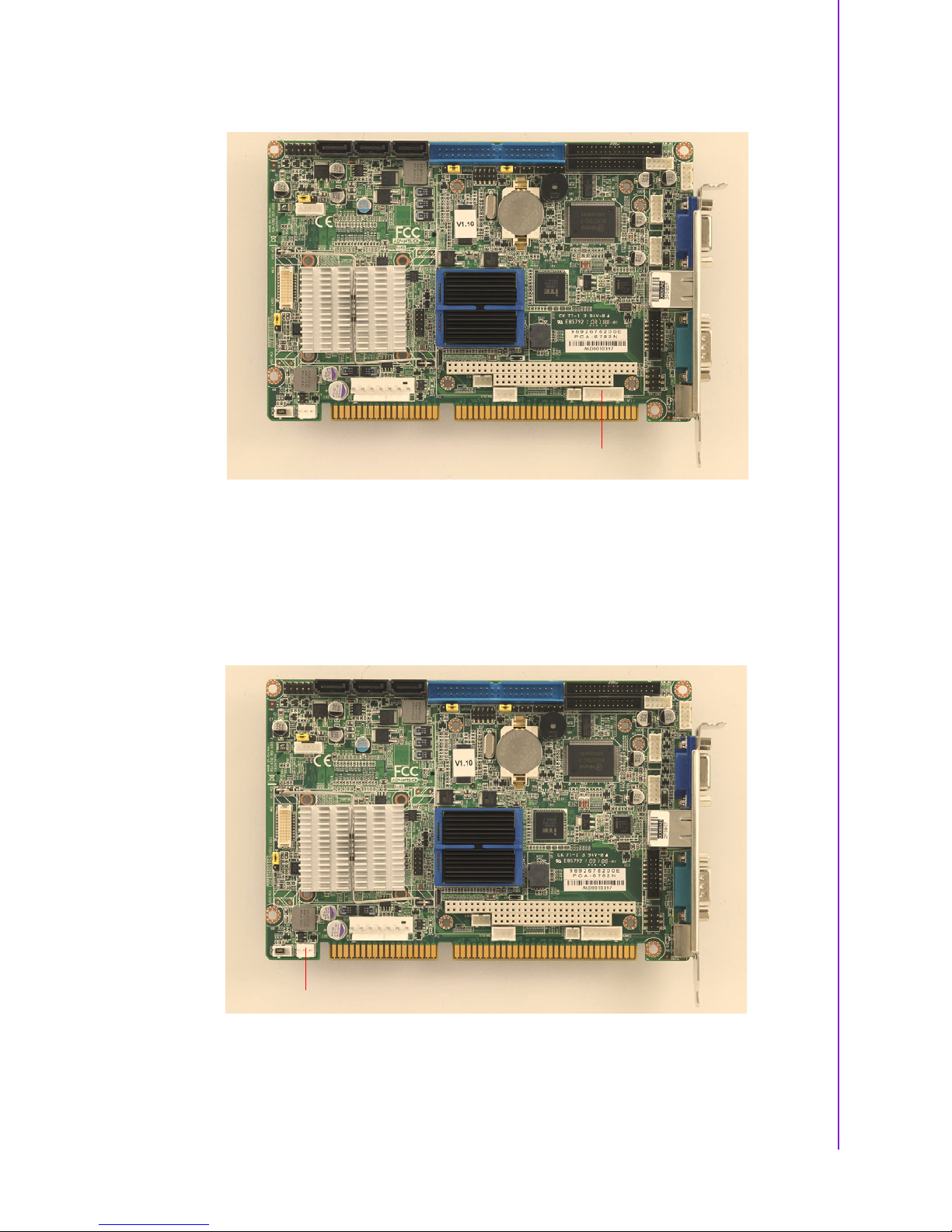
Figure 2.6 PS/2 Keyboard/Mouse Connector (KBMS1)
One 6-pin mini-DIN connector (KBMS1) on the card mounting bracket provides connection to a PS/2 keyboard or a PS/2 mouse, respectively. KBMS1 can also be connected to an adapter cable (P/N: 1700060202) for connecting to both a PS/2
keyboard and a PS/2 mouse.
KBMS1
Page 28
17 PCA-6782 User Manual
Chapter 2 Connecting Peripherals & Jumper Settings
2.8 External Keyboard Pin Header (KBMS2)
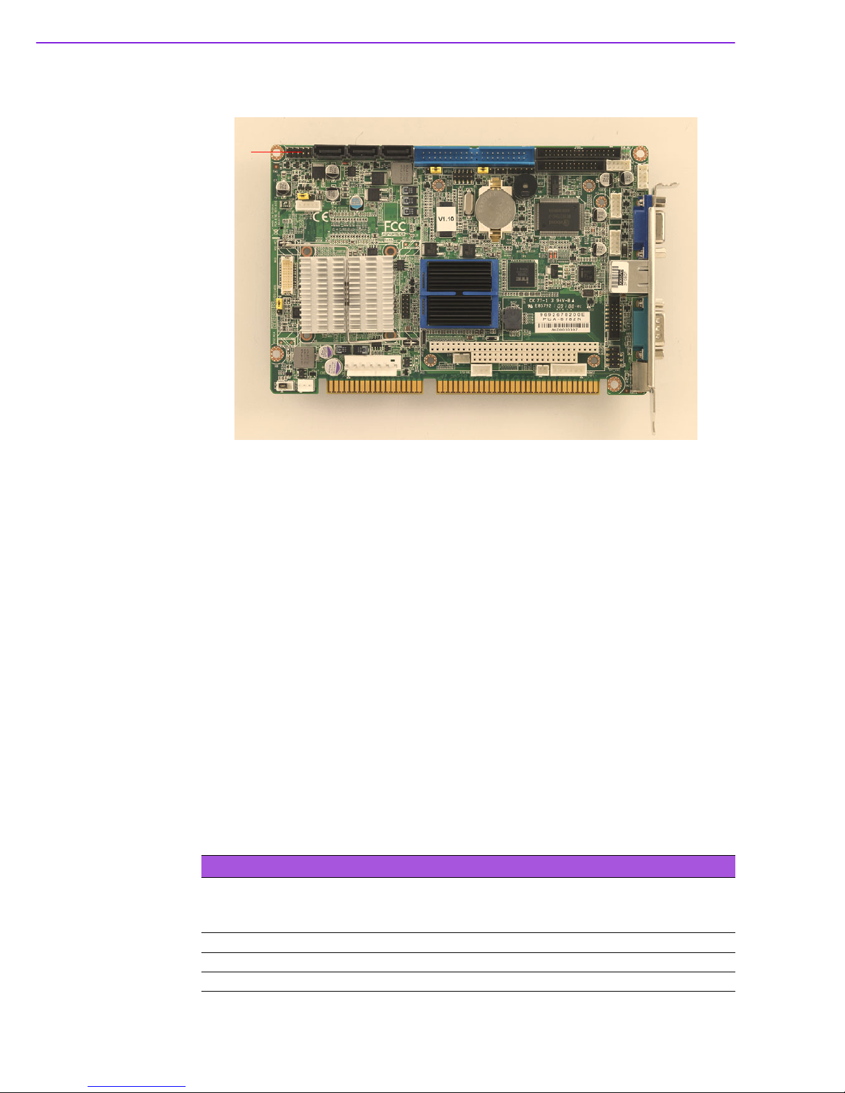
Figure 2.7 External Keyboard Connector (KBMS2)
In addition to the PS/2 mouse/keyboard connector on the PCA-6782's rear plate,
there is also an extra onboard external keyboard pin header. This gives system integrators greater design flexibility.
2.9 CPU Fan Connectors (CPUFAN1)
Figure 2.8 CPU Fan Connectors (CPUFAN1)
This connector supplies power and fan speed signal to PCA-6782D's proprietary
CPU cooler for Atom D525 CPU.
KBMS2
CPUFAN1
Page 29
PCA-6782 User Manual 18
2.10 Front Panel Connectors (JFP1)
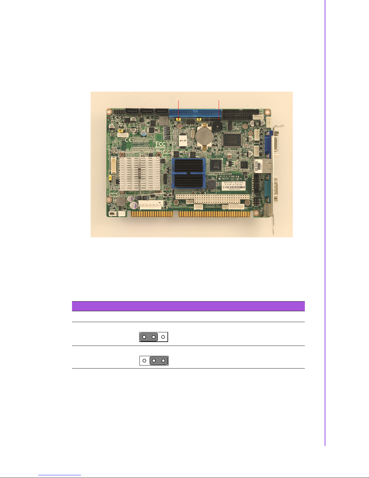
Figure 2.9 Front Panel Connectors (JFP1)
There are several external indicators and switches to help monitor and control the
PCA-6782.
2.10.1 ATX Power Button (JFP1 Pin 9~10)
If your computer case is equipped with an ATX power supply, you should connect the
power on/off button on your computer case to (JFP1 Pin 9~10). This connection
enables you to turn your computer on and off.
2.10.2 Reset (JFP1 Pin 7~8)
Many computer cases offer the convenience of a reset button. Connect the wire for
the reset button.
2.10.3 Suspend LED (JFP1 Pin 5~6)
You can connect an LED to connector (JFP1 Pin 5~6) to indicate when the system is
in suspend status.
2.10.4 Power LED and keyboard lock connector (JFP1 Pin 3~4)
(JFP1 Pin 3~4) is a for the power on LED. Refer to Appendix B for detailed information on the pin assignments.
JFP1
Table 2.1: ATX power supply LED status (No support for AT power)
Power mode
LED (ATX Power mode)
(On/off by tentative
button)
LED (AT Power mode)
(On/off by switch of
Power supply)
LED (AT Power
mode) (On/off by
front panel Switch)
System On On On On
System Suspend Fast flashes Fast flashes Fast flashes
System Off Slow flashes Off Off
Page 30
19 PCA-6782 User Manual
Chapter 2 Connecting Peripherals & Jumper Settings
2.10.5 HDD LED (JFP1 Pin 1~2)
You can connect an LED to connector (JFP1 Pin 1~2) to indicate when the HDD is
active.
2.11 Watch Dog Timer (JWDT1) / Infrared (JIR1)
Figure 2.10 Watch Dog Timer (JWDT1) / Infrared (JIR1)
2.11.1 Watchdog timer output (JWDT1)
The PCA-6782 contains a watchdog timer that will reset the CPU in the event the
CPU stops processing. This feature means the PCA-6782 will recover from a software failure or an EMI problem. The JWDT1 jumper settings control the outcome of
what the computer will do in the event the watchdog timer is tripped.
2.11.2 Infrared Connector (JIR1)
This 5-pin header is for connecting infrared device connector.
JWDT1
JIR1
Table 2.2: Watchdog timer output (JWDT1)
Function Jumper Setting
IRQ11
* System Reset
* default setting
1 - 2 closed
123
2 - 3 closed
1 23
Page 31
PCA-6782 User Manual 20
2.12 Single Giga LAN RJ45 connector (LAN1)
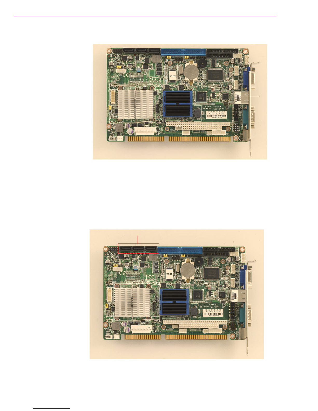
Figure 2.11 Single Giga LAN RJ45 connector (LAN1)
PCA-6782 uses the Intel
®
82567V Gigabit LAN chips are linked to dedicated PCIe x1
lanes. PCA-6782 provide high throughputs for heavy loading networking environment. It provides one RJ-45 connectors in the rear side and is convenient for most
industrial applications.
2.13 Serial ATA interface (SATA1 ~ SATA3)
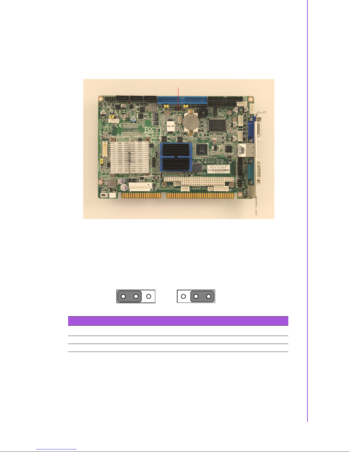
Figure 2.12 Serial ATA interface (SATA1 ~ SATA3)
LAN1
SATA1 ~ 3
Page 32
21 PCA-6782 User Manual
Chapter 2 Connecting Peripherals & Jumper Settings
In addition to the EIDE interface (up to two devices), the PCA-6782 features three
high performance Serial ATA interfaces (up to 300 MB/s) for easy hard drive cabling
with long, thin SATA cables.
2.14 GPIO header (GPIO1)
Figure 2.13 GPIO header (GPIO1)
PCA-6782 provides a 10-pin header for Digital I/O usage. Refer to Appendix B for
detailed information on the pin assignments and programming guide in Appendix C.
2.15 LVDS panel power selection (JLVDS1)
* default setting
GPIO1
Table 2.3: LVDS panel power selection (JLVDS1)
Ping Function
1-2 (default) +3.3 V*
2-3 +5 V
123
1 23
Page 33
PCA-6782 User Manual 22
2.16 LVDS VBR selection (JVBR1)
* default setting
2.17 CMOS clear (CMOS1)
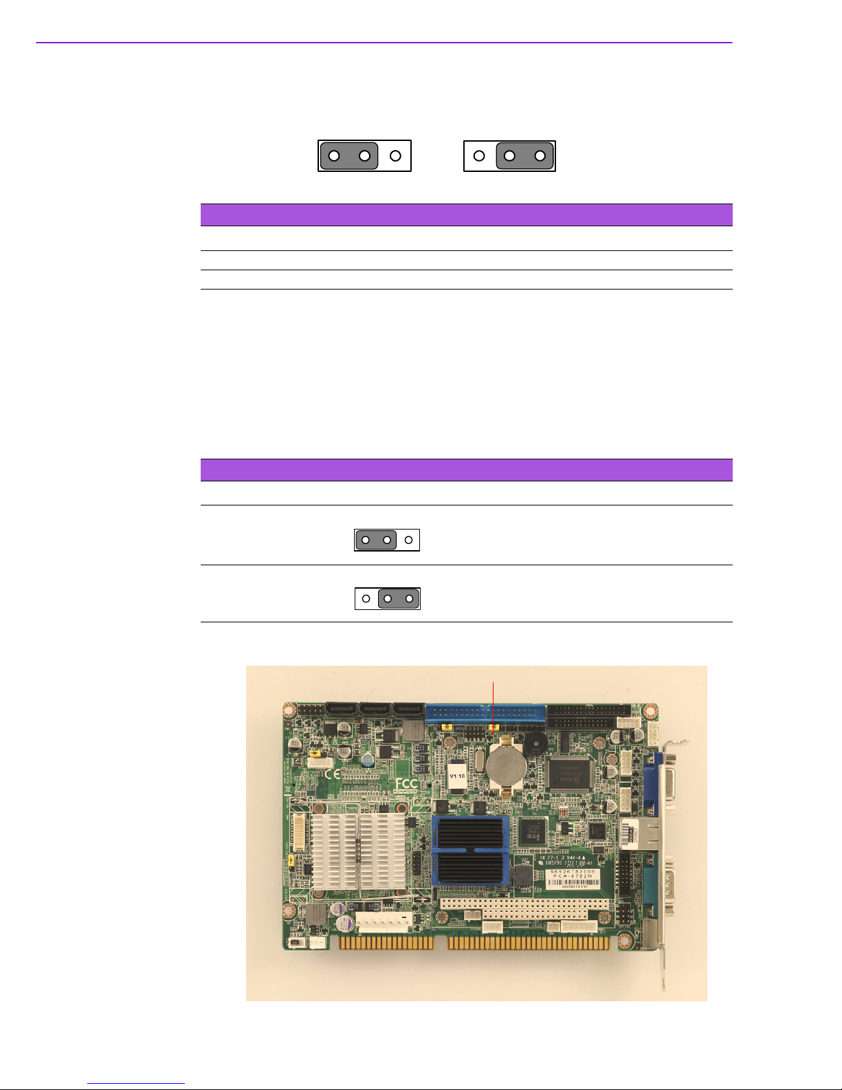
The PCA-6782 single board computer contains a jumper that can erase CMOS data
and reset the system BIOS information. Normally this jumper should be set with pins
1-2 closed. If you want to reset the CMOS data, set CMOS1 to 2-3 closed for just a
few seconds, and then move the jumper back to 1-2 closed. This procedure will reset
the CMOS to its default setting.
Table 2.4: LVDS VBR selection (JVBR1)
Ping Function
1-2 * Linear way to control brightness*
2-3 PWM to control brightness
123
1 23
Table 2.5: CMOS (CMOS1)
Function Jumper Setting
* Keep CMOS data
Clear CMOS data
* default setting
1 - 2 closed
123
2 - 3 short
1 23
CMOS1
Page 34
23 PCA-6782 User Manual
Chapter 2 Connecting Peripherals & Jumper Settings
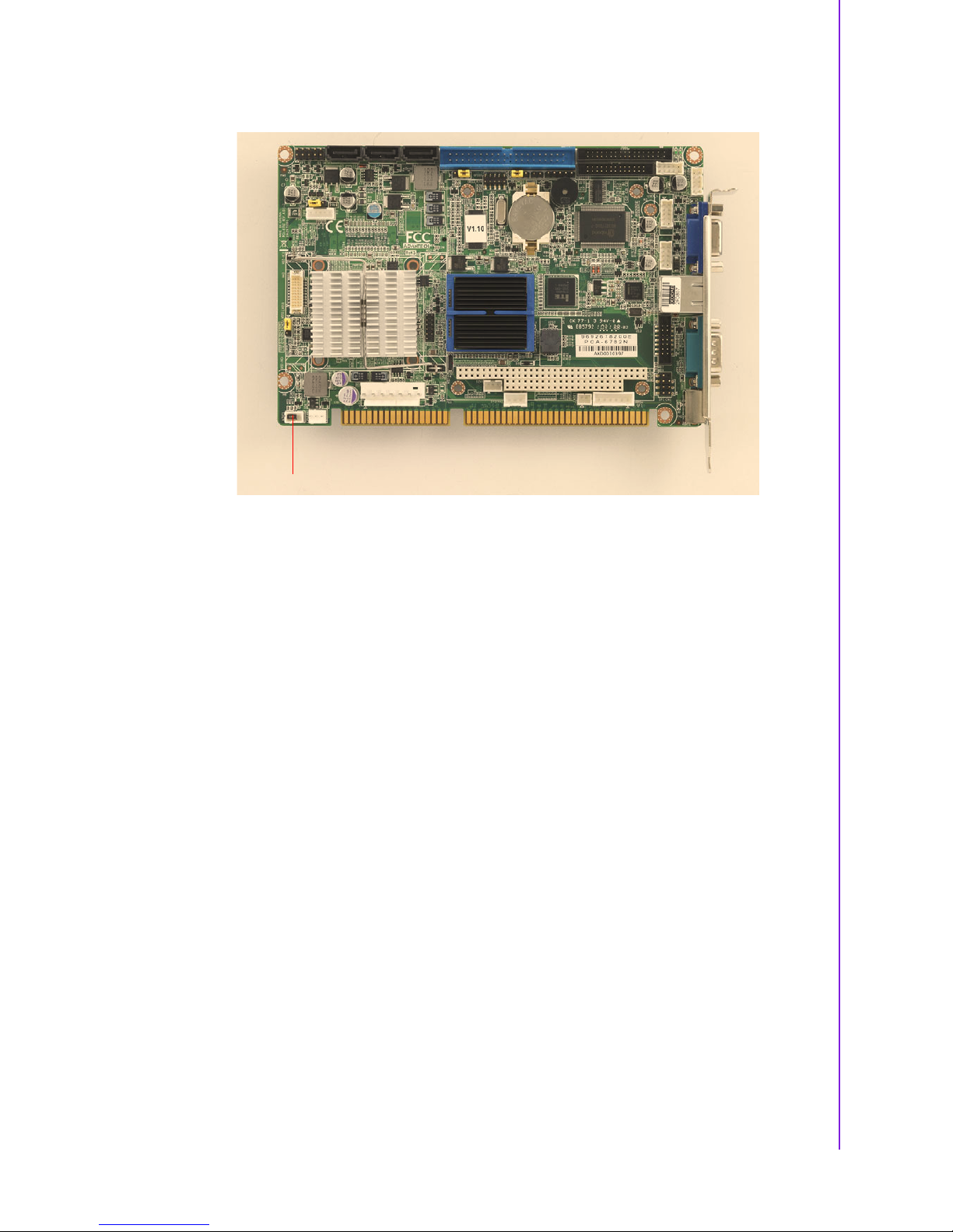
2.18 ATX Feature connector(ATXF1)
The PCA-6782 can support an advanced soft power switch function. When using an
ATX power supply, please follow the instructions below to enable ATX functions.
1. Find ATX feature cable (1700002343).
2. Connect the 3-pin plug of the cable to ATXF1 (ATX feature connector). And con-
nect another plug to backplane HCN1 connector.
3. Connect the power on/off button cable of the chassis to JPF1’s pins 9 and 10.
Default value is set ATXF1 to short pin1-2 to support AT power.
Important: Make sure that the ATX power supply can take at least a 10mA load on
the 5 V standby lead (5 VSB). If not, you may have difficulty powering on your system.
ATXF 1
Page 35
PCA-6782 User Manual 24
2.19 ATX power control connector (ATX1)
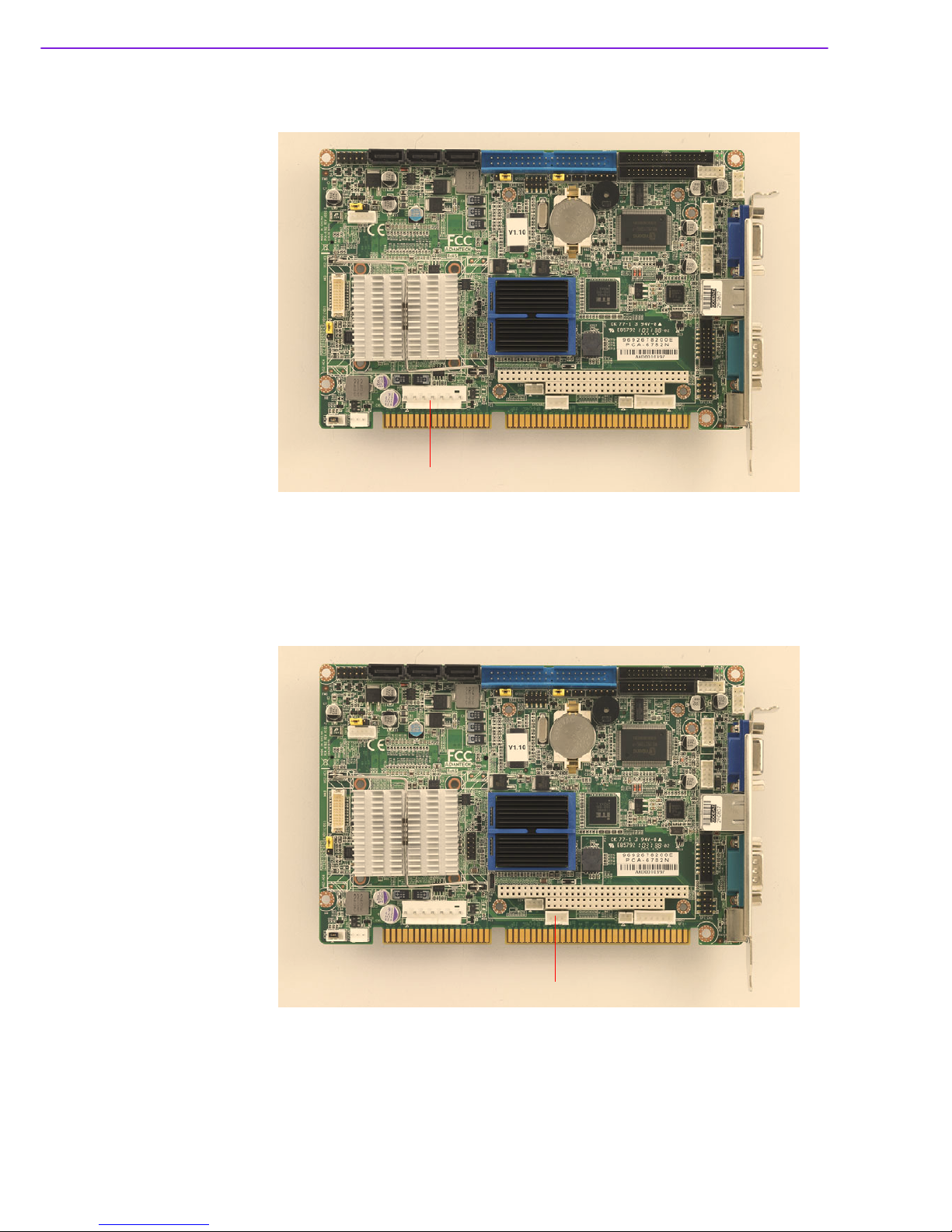
The PCA-6782 supports ATX power supply. ATX1 supplies main power (+5 V,+12 V,
5 VSB), and it is a 6 x 2 power connector.
2.20 System FAN connector (SYSFAN1)
The PCA-6782 is equipped with a 3-pin FAN connector providing +12 V power for
system FAN.
ATX1
SYSFAN1
Page 36
25 PCA-6782 User Manual
Chapter 2 Connecting Peripherals & Jumper Settings
2.21 LVDS Signal and Power Connectors (LVDS1)
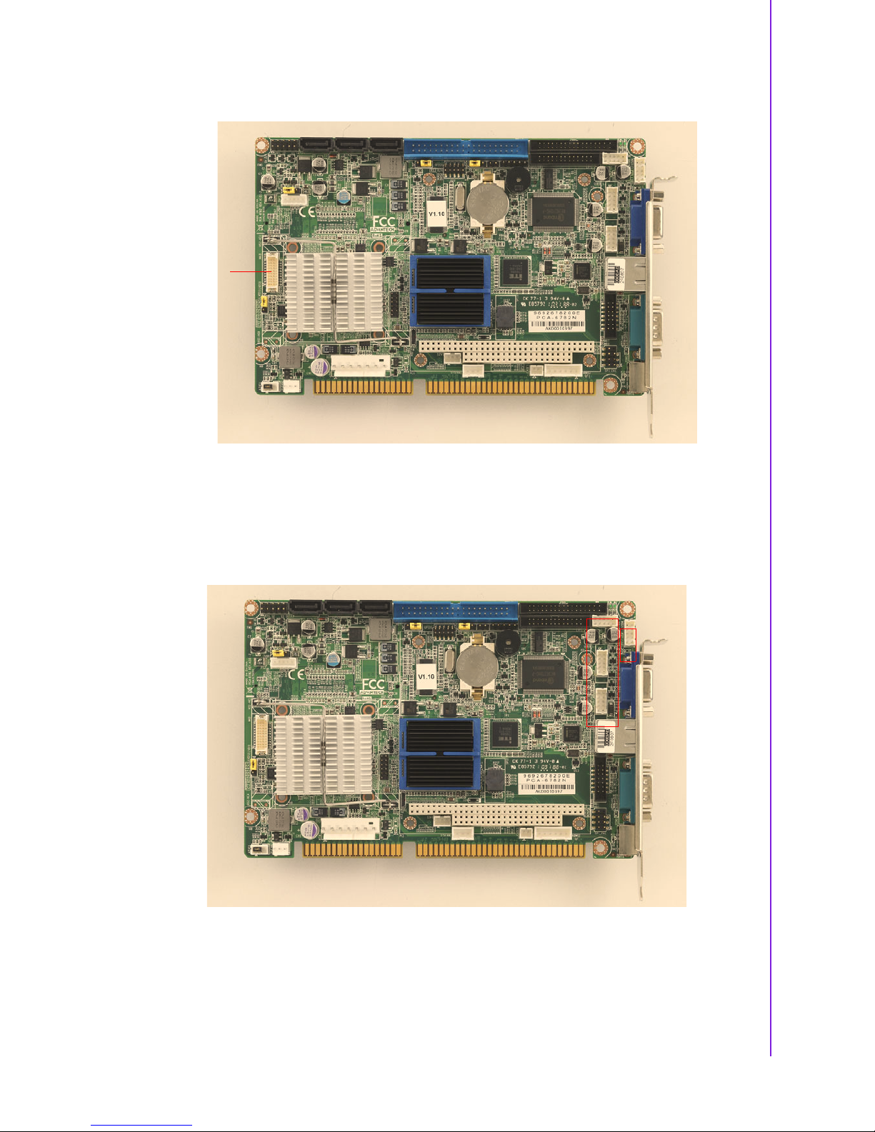
For PCA-6782, LVDS1 consists of a 20-pin connector which can support 18-bit single
channel LVDS with resolution up to WXGA (1366 x 768 or 1280 x 800).
2.22 USB Ports (USB 1 ~ 8)
PCA-6782 supports 8 USB 2.0 ports, you may use the 1700008887 4-port USB cable
kit to utilize any four of USB 1~8.
LVDS 1
Page 37
PCA-6782 User Manual 26
2.23 CF Card Socket
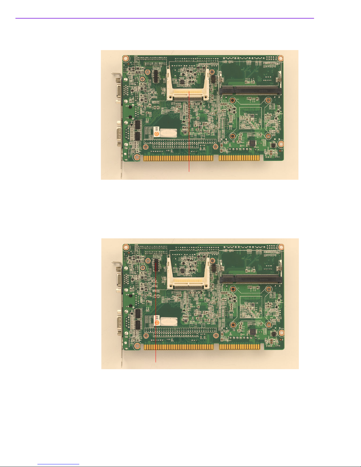
PCA-6782 supports a CF card device, an installed CF card will occupy the master
IDE device. Please locate it on the solder side of the CPU card.
2.24 Low Pin Count Device Connection Pin Header
PCA-6782 has a 14-pin female pin header on its solder side to support &20SRUW
extension modules. You may purchase them to add 4 more RS-485 serialSRUWV
(COM ports) with auto flow control function. Please see ordering information
be
low.
Part Number and Description:
PCA-COM485-00A1E: Four RS 422/485 COM module WITH auto flow control function.
CF1
LPC1
Page 38

Chapter 3
3 AMI BIOS Setup
Page 39
PCA-6782 User Manual 28
AMI BIOS has been integrated into many many motherboards, and has been very
popular for well over a decade. People sometimes refer to the AMI BIOS setup menu
as BIOS, BIOS setup or CMOS setup.
With the AMI BIOS Setup program, you can modify BIOS settings and control the
special features of your computer. The BIOS Setup program uses a number of
menus for making changes and turning special features on or off. This chapter
describes the basic navigation of the PCA-6782 setup screens.
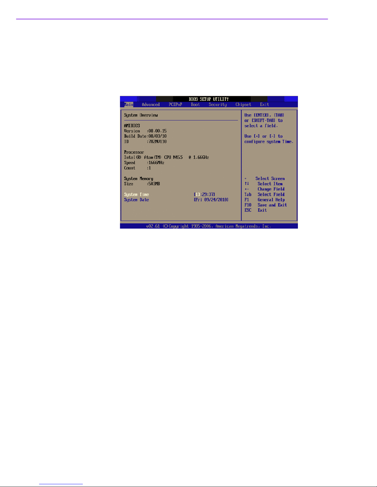
Figure 3.1 Setup Program Initial Screen
AMI's BIOS ROM has a built-in Setup program that allows users to modify the basic
system configuration. This information is stored in battery-backed up CMOS and it is
retained when the power is turned off.
Page 40
29 PCA-6782 User Manual
Chapter 3 AMI BIOS Setup
3.1 Entering Setup
Press the "Del" key during the Power On Self Test (POST) process to enter the BIOS
setup screen, otherwise the system will continue the POST process.
3.2 Main Setup
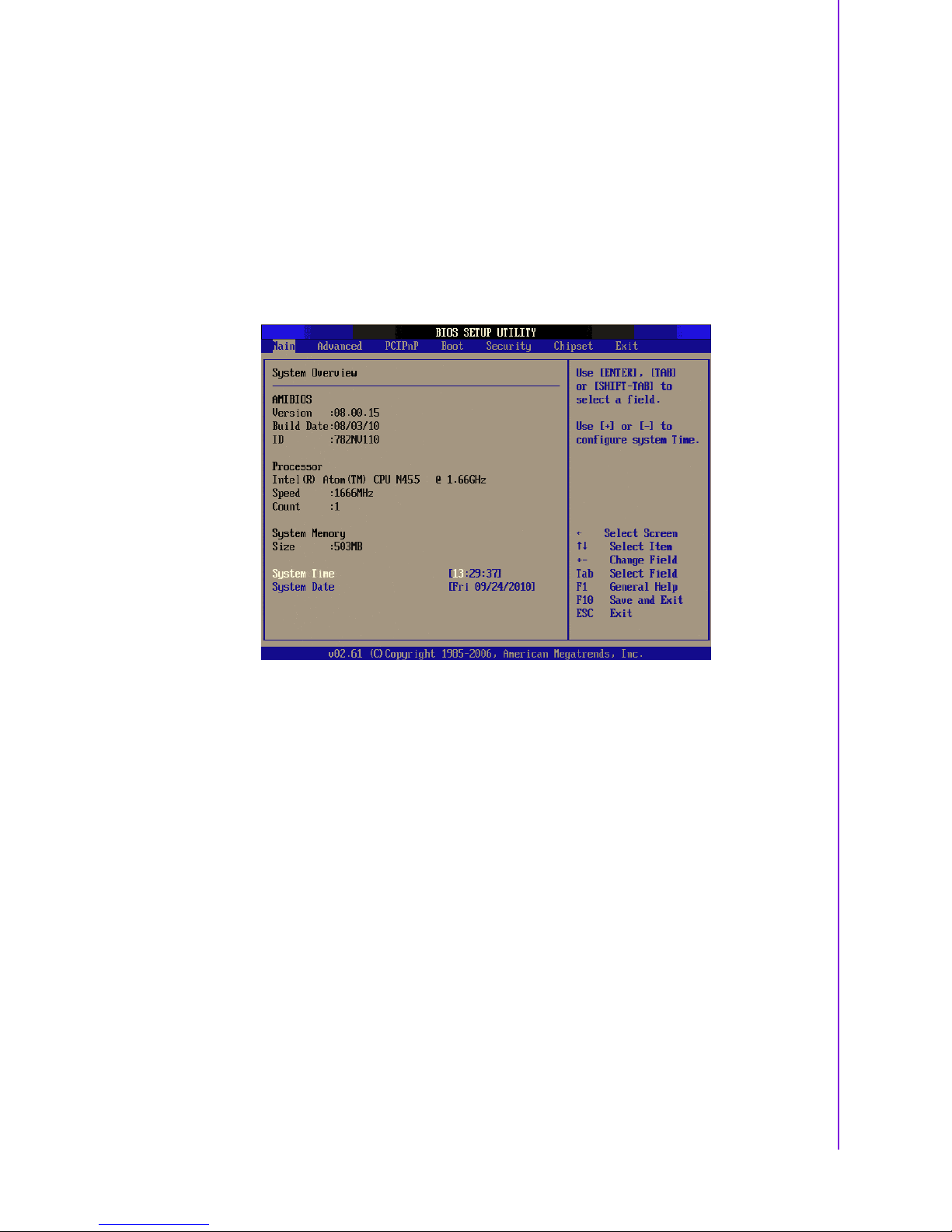
When you first enter the BIOS Setup Utility, you will enter the Main setup screen. You
can always return to the Main setup screen by selecting the Main tab. There are two
Main Setup options. They are described in this section. The Main BIOS Setup screen
is shown below.
Figure 3.2 Main Setup Screen
The Main BIOS setup screen has two main frames. The left frame displays all the
options that can be configured. Grayed-out options cannot be configured; options in
blue can. The right frame displays the key legend.
Above the key legend is an area reserved for a text message. When an option is
selected in the left frame, it is highlighted in white. Often a text message will accompany it.
3.2.1 System time / System date
Use this option to change the system time and date. Highlight System Time or System Date using the <Arrow> keys. Enter new values through the keyboard. Press the
<Tab> key or the <Arrow> keys to move between fields. The date must be entered in
MM/DD/YY format. The time must be entered in HH:MM:SS format.
Page 41
PCA-6782 User Manual 30
3.3 Advanced BIOS Features Setup
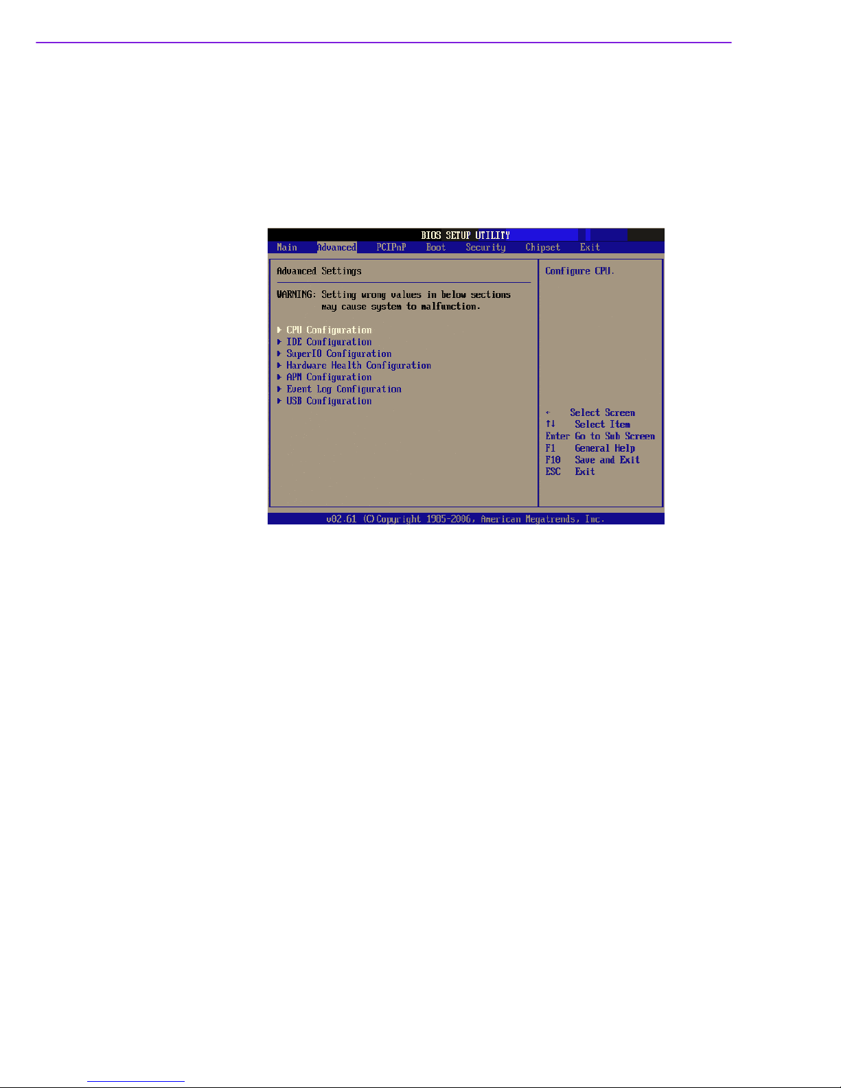
Select the Advanced tab from the PCA-6782 setup screen to enter the Advanced
BIOS Setup screen. You can select any of the items in the left frame of the screen,
such as CPU Configuration, to go to the sub menu for that item. You can display an
Advanced BIOS Setup option by highlighting it using the <Arrow> keys. All Advanced
BIOS Setup options are described in this section. The Advanced BIOS Setup screen
is shown below. The sub menus are described on the following pages.
Figure 3.3 Advanced BIOS Features Setup Screen
Page 42
31 PCA-6782 User Manual
Chapter 3 AMI BIOS Setup
3.3.1 CPU Configuration
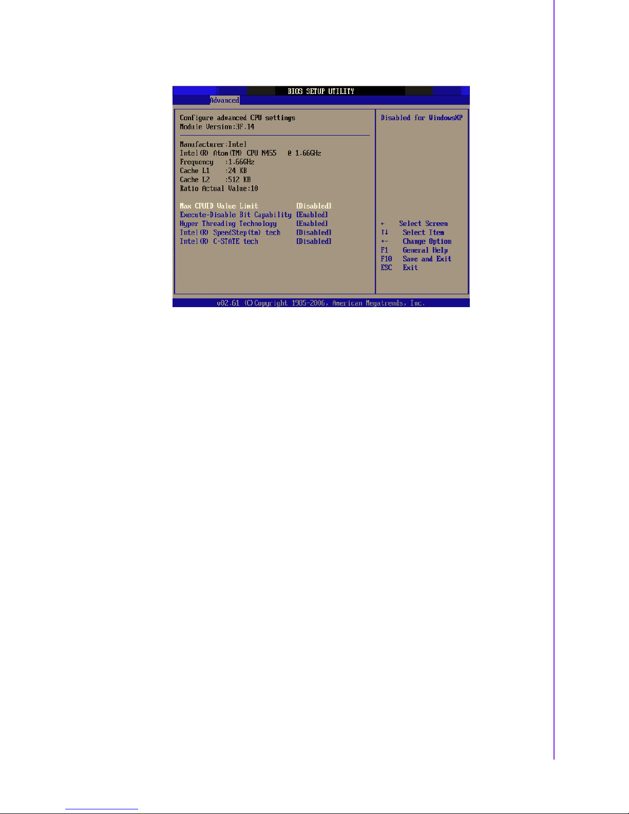
Figure 3.4 CPU Configuration Settings
! Max CPUID Value Limit
This is disabled for Windows XP.
! Execute Disable Bit
This item specifies the Execute Disable Bit Feature. The settings are Enabled
and Disabled. The Optimal and Fail-Safe default setting is Enabled. If Disabled
is selected, the BIOS forces the XD feature flag to always return to 0.
! Hyper-Threading Technology
While using a CPU with Hyper-Threading technology, you can select "Enabled"
to enable Hyper-Threading Technology in an OS which supports Hyper-Threading Technology or select "Disabled" for other OSs which do not support HyperThreading technology.
! Intel® SpeedStep
TM
tech
Intel SpeedStep Technology centralizes the control mechanism in the processor, eliminating the need for coordination with the chipset during the frequency/
voltage configuration. This option is used to enable/disable the GV3 bit.
! Intel® C-STATE tech
Intel® CPU Enhanced Halt (C1E) function, a function to save CPU power consumption in system halt state. When enabled, the CPU speed and voltage will
be reduced during system halt state to save power consumption. You may
choose to enable or disable it.
Page 43
PCA-6782 User Manual 32
3.3.2 IDE Configuration
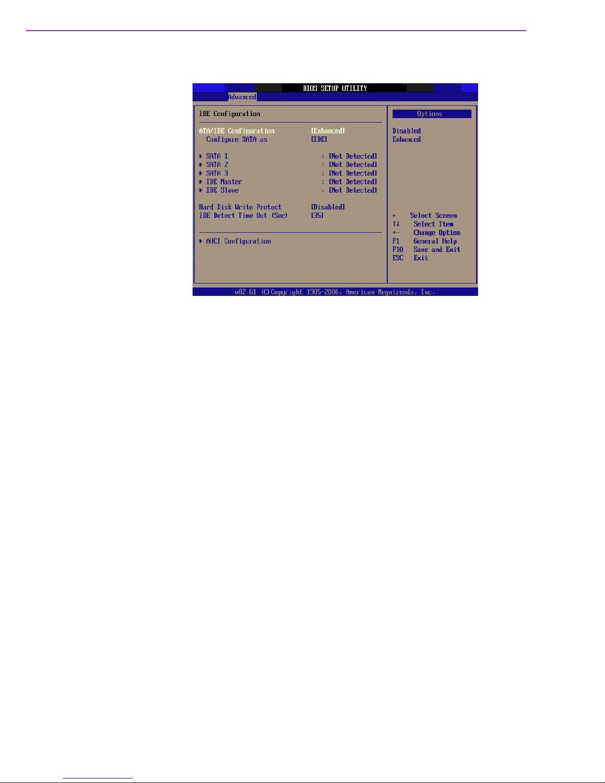
Figure 3.5 IDE Configuration
! ATA/IDE Configuration
This can be configured as Disabled or Enhanced.
! Configure SATA as
This can be configured as IDE or AHCI.
! SATA1/SATA2/SATA3
While entering setup, the BIOS automatically detects the presence of SATA
devices. This displays the status of SATA device auto-detection.
! IDE Master / Slave
While entering setup, the BIOS automatically detects the presence of IDE
devices. This displays the status of IDE device auto-detection.
! AHCI Configuration
AHCI is a new interface specification that allows the SATA controller driver to
support advanced features. While entering setup, BIOS auto detects the presence of AHCI devices. This displays the status of auto detection of AHCI
devices.
Page 44
33 PCA-6782 User Manual
Chapter 3 AMI BIOS Setup
3.3.3 Super I/O Configuration
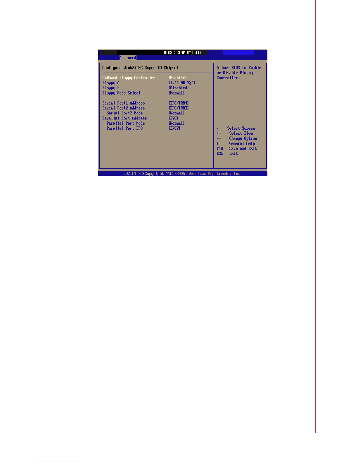
Figure 3.6 Super I/O Configuration
! OnBoard Floppy Controller
Enable or disable the floppy function.
! Floppy A
Select the type of floppy drive connected to the system. We suggest you disable the floppy if installing Windows Vista without a floppy drive.
! Floppy B
Select the type of floppy drive connected to the system.
! Floppy Mode Select
For user to set floppy mode, this must match specification of the floppy drive
connected to CPU card, available options are 360 KB 5 1/4", 1.2 MB 5 1/4", 720
KB 3 1/2", 1.44 MB 3 1/2", 2.88 MB 3 1/2".
! Serial Port1 Address
This option configures serial port 1 base addresses.
! Serial Port2 Address
This option configures serial port 2 base addresses. The following options are
also available:
– Serial port2 Mode
This option configures serial port 2 mode. Available options include Normal,
IrDA, ASK IR.
! Parallel Port Address
This configures parallel port base addresses. The following options are also
available:
– Parallel Port Mode
This option configures Parallel Port mode. Available options include Normal,
Bi-directional, ECP, EPP, ECP & EPP.
– Parallel Port IRQ
This option configures s Parallel Port base IRQ.
Page 45
PCA-6782 User Manual 34
3.3.4 Hardware Health Function
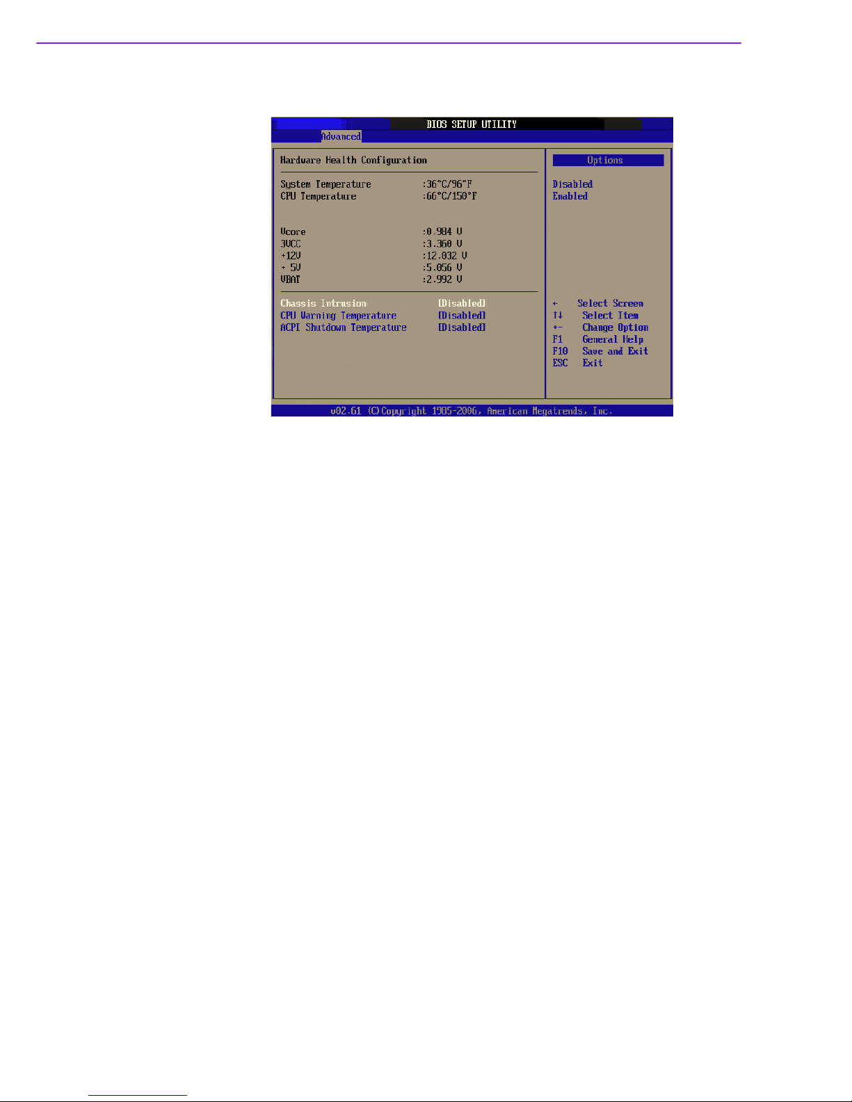
Figure 3.7 Hardware Health Configuration.
! Hardware health function
Enable/Disable the onboard hardware monitor controller. If this option is
enabled, the BIOS and OBS utility can get the system board's health information from hardware monitor controller.
! Chassis Intrusion
Enable/Disable the Chassis Intrusion monitoring function. When the case is
opened, the buzzer beeps.
! CPU warning temperature
Use this to set the CPU warning temperature threshold. When the system
reaches the warning temperature, the buzzer will beep.
! ACPI Shut Down Temperature
This potion allows user to set the CPU temperature at that the system will automatically shut down for preventing CPU from over heat damage.
Page 46
35 PCA-6782 User Manual
Chapter 3 AMI BIOS Setup
3.3.5 APM Configuration
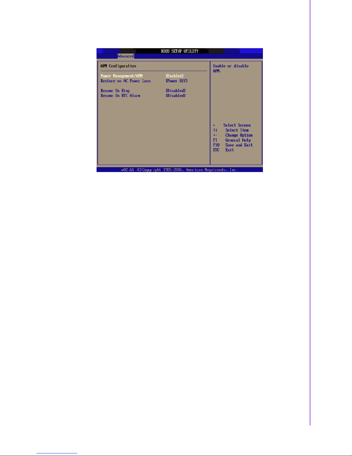
Figure 3.8 APM Configuration
! Power Management/APM
Enable or disable APM power management function.
! Restore on AC Power Loss
This option allows user to set system action when AC power restores after AC
power loss. Available options include Power Off, Power On, Last Status.
! Resume On Ring
Disable/Enable RI wake event.
! Resume On RTC Alarm
Disable/Enable RTC wake event.
Page 47
PCA-6782 User Manual 36
3.4 Event Logging Details
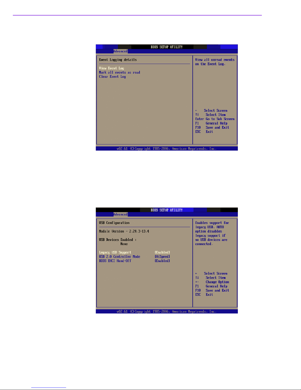
Figure 3.9 Event Logging Details
! View Event Log
3.5 USB Configuration
Figure 3.10 USB Configuration
Page 48
37 PCA-6782 User Manual
Chapter 3 AMI BIOS Setup
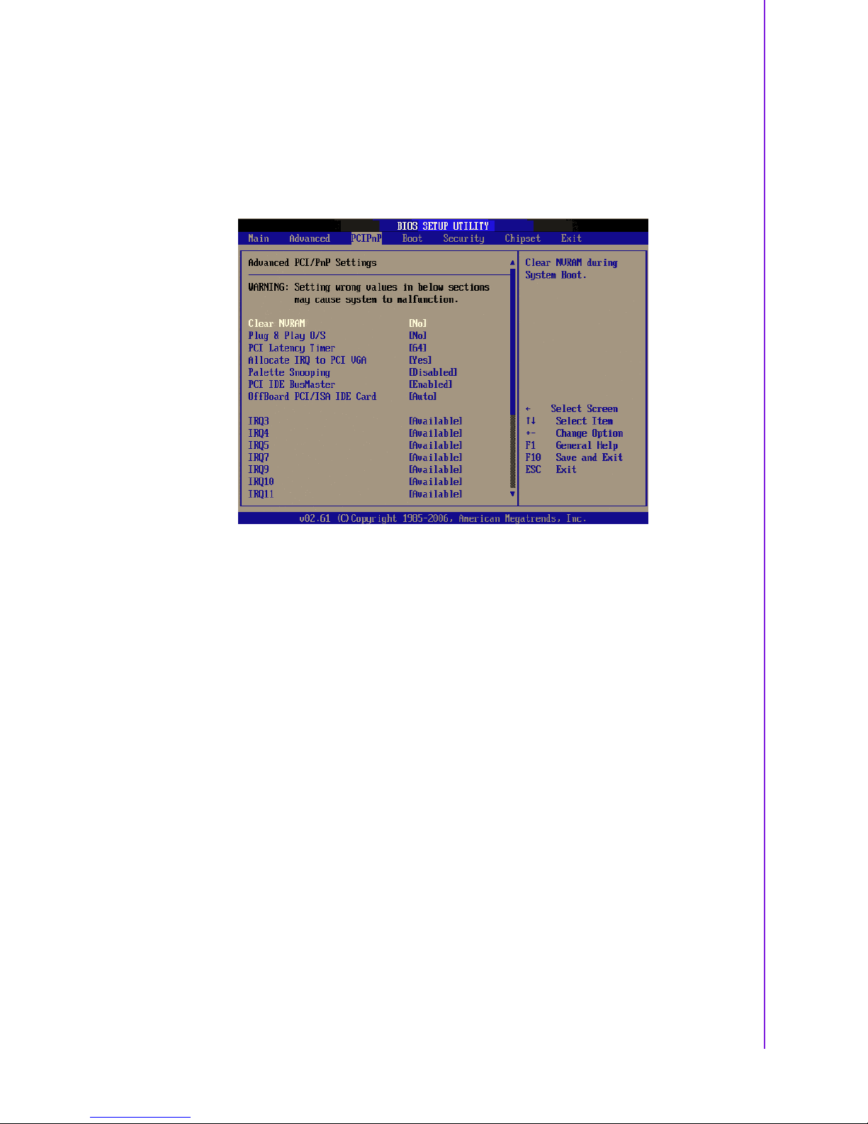
3.6 PCI/PNP Setup
Select the PCI/PnP tab from the PCA-6782 setup screen to enter the Plug and Play
BIOS Setup screen. Highlighting a Plug and Play BIOS Setup option by using the
<Arrow> keys displays a description in the right-hand panel. All Plug and Play BIOS
Setup options are described in this section. The Plug and Play BIOS Setup screen is
shown below.
Figure 3.11 PCI/PNP Setup
! Clear NVRAM
Set this value to force the BIOS to clear the Non-Volatile Random Access Memory (NVRAM). The Optimal and Fail-Safe default setting is No.
! Plug and Play O/S
Set this value to allow the system to modify the settings for Plug and Play operating system support. The Optimal and Fail-Safe default setting is No.
! PCI Latency Timer
Use this to adjust the PCI Latency Timer. This option sets the latency of all PCI
devices on the PCI bus. The Optimal and Fail-Safe default setting is 64.
! Allocate IRQ to PCI VGA
Set this value to allow or stop the system from giving the VGA adapter card an
interrupt address. The Optimal and Fail-Safe default setting is Yes.
! Palette Snooping
Set this value to allow the system to modify the Palette Snooping settings. The
Optimal and Fail-Safe default setting is Enabled.
! PCI IDE BusMaster
Set this value to allow or prevent the use of PCI IDE Busmastering. The Optimal and Fail-Safe default setting is enabled.
! Off Board PCI/ISA IDE card
Set this value to allow an add-on PCI/ISA IDE card to be selected. The Optimal
and Fail-Safe default setting is Auto.
Page 49
PCA-6782 User Manual 38
! IRQ
– IRQ[3,4,5,7,9,10,11,14,15]:
Available: Specified IRQ is available to be used by PCI/PnP devices.
Reserved: Specified IRQ is reserved for use by Legacy ISA devices.
DMA Channel [0,1,3,5,6,7]:
– Available: Specified DMA is available to be used by PCI/PnP devices.
Reserved: Specified DMA is reserved for use by legacy ISA devices.
Reserved Memory Size: Size of memory block to reserve for legacy ISA
devices.
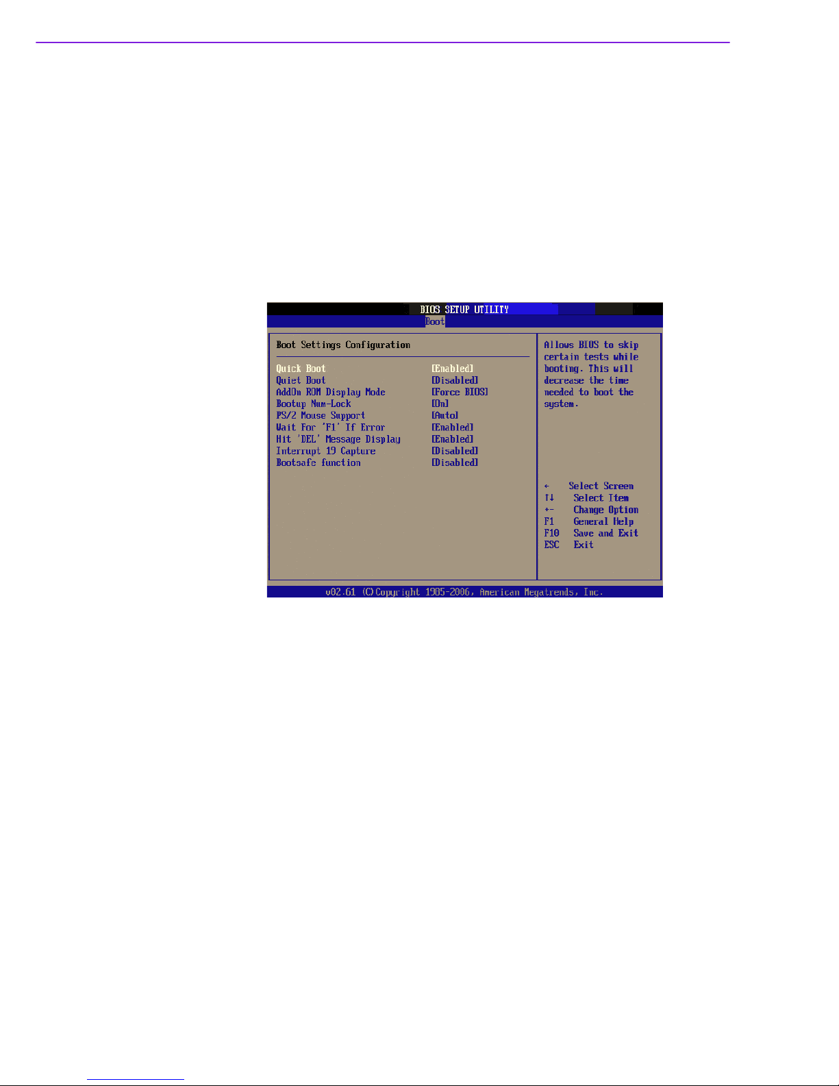
3.7 Boot Setup Utility
Figure 3.12 Boot Settings Configuration
The following options are available:
! Quick Boot
Allows the BIOS to skip certain tests while booting. This will decrease the time
needed to boot the system.
! Quiet Boot
If this option is set to Disabled, the BIOS displays normal POST messages. If
Enabled, an OEM Logo is shown instead of POST messages.
! AddOn ROM Display Mode
This is for choosing display mode of option ROM information under DOS environment during booting up process. Available options include Force BIOS,
Keep Current.
! Bootup Num-Lock
Select the Power-on state for Numlock.
! PS/2 Mouse Support
Enable or disable PS/2 interface mouse support. Available options include
Auto, Enable, Disable.
! Wait For ‘F1’ If Error
Wait for the F1 key to be pressed if an error occurs.
Page 50
39 PCA-6782 User Manual
Chapter 3 AMI BIOS Setup
! Hit ‘DEL’ Message Display
Displays “Press DEL to run Setup” in POST.
! Interrupt 19 Capture
Enable or disable option ROM to trap interrupt 19.
! Bootsafe function
Enable or disable
proprietary Bootsafe function. (only reserve this
ite
m. If need this function, need customize BIOS).
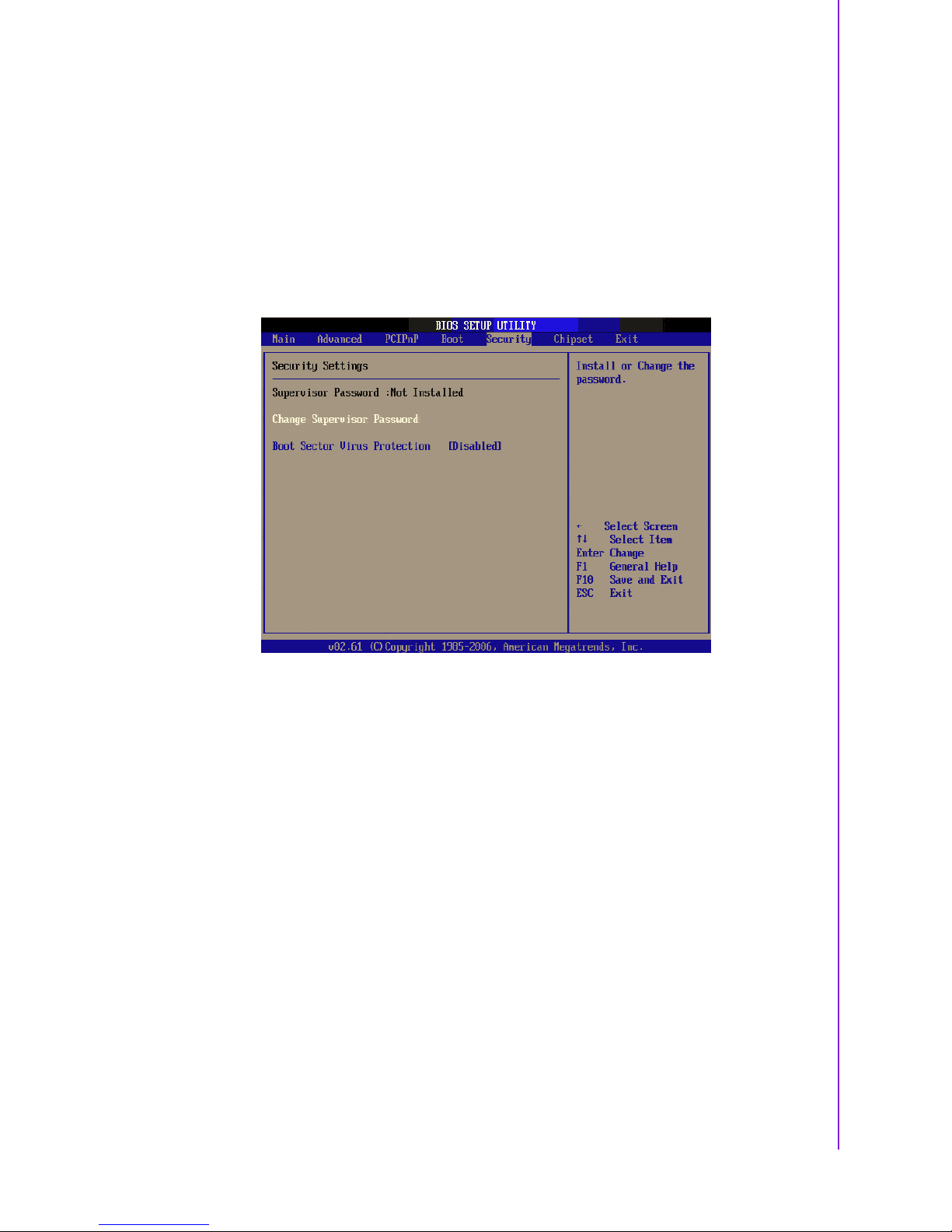
3.8 Security Setup
Figure 3.13 Password Configuration
Select Security Setup from the PCA-6782 Setup main BIOS setup menu. All Security
Setup options, such as password protection and virus protection are described in this
section. To access the sub menu for the following items, select the item and press
<Enter>:
! Change Supervisor Password
Provides for either installing or changing the password.
! Boot sector Virus protection: The boot sector virus protection will warn if any
program tries to write to the boot sector.
Page 51
PCA-6782 User Manual 40
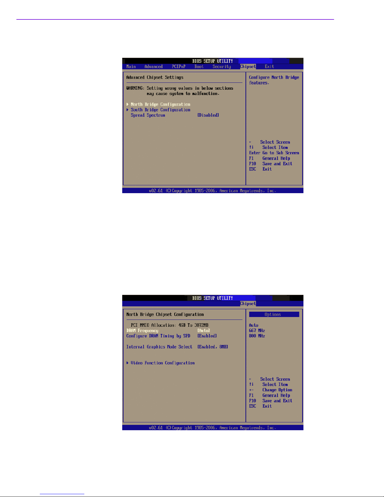
3.9 Advanced Chipset Settings
Figure 3.14 Advanced Chipset Settings
! North Bridge Configuration
Allows user to set graphic and memory controller configurations.
! South Bridge Configuration
Allows user to set I/O port configurations.
! Spread Spectrum
Enable/Disable spread spectrum. Enable spread spectrum function can have
better EMI compatibility but may cause some unexpected peripheral device
incompatibility issue.
Page 52
41 PCA-6782 User Manual
Chapter 3 AMI BIOS Setup
! DRAM Frequency
Allows user to set DDR2 memory operating frequency.
! Configure DRAM Timing by SPD
Allows user to set DRAM operating timing coefficients by SPD or Manual.
! Internal Graphics Mode Select
Allows user to set graphic mode for DOS environment. Available options
include Disable, Enable 4MB, Enable 8MB.
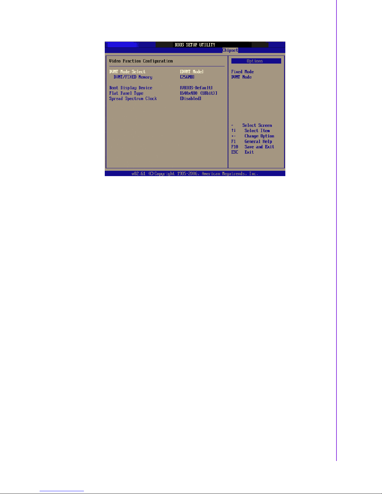
! Video Function Configuration
This allows user to set IGD (Integrated Graphics Device) configuration.
! DVMT model select
Displays the active system memory mode.
! DVMT / FIXED Memory
Specify the amount of DVMT / FIXED system memory to allocate for video
memory.
! Flat Panel Type
Allows user to set LVDS panel resolution and signal width. This should match
the specification of LVDS panel connected to the CPU card.
! Spread Spectrum Clock
Enable/Disable Spread Spectrum Clock. Enable spread spectrum function can
have better EMI compatibility but may cause some unexpected peripheral
device incompatibility issue.
Page 53
PCA-6782 User Manual 42
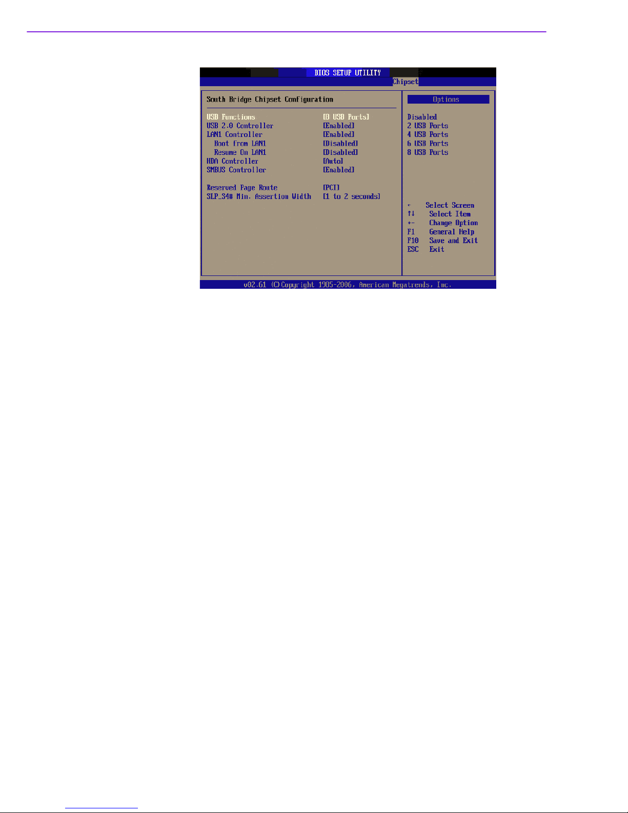
Figure 3.15 Souh Bridge Configuration
! USB Functions
Select: Disabled, 2 USB Ports, 4 USB Ports, 6 USB Ports or 8 USB Ports.
! USB 2.0 Controller
Enables or disables the USB 2.0 controller.
! LAN 1 Controller
Enables or disables the LAN 1 GbE controller. The options below are also available.
– Boot from LAN1
Allows user to enable or disable the function of LAN booting from a PXE
server.
– LAN1 Wake Up From S5
Enables or disables LAN1 Wake Up From S5 function.
! HDA Controller
Enables or disables the High Definition audio controller.
! SMBUS Controller
Enables or disables the SMBUS controller.
! Reserved Page Route
Allows user to set Port 80 information output port. Available options include
PCI, LPC.
! SLP_S4# Min. Assertion Width
This is for setting delay time between stand by power readiness and ICH
SLP_S4# signal triggering. Available options include 1 to 2 seconds, 2 to 3 seconds, 3 to 4 seconds, 4 to 5 seconds.
Page 54
43 PCA-6782 User Manual
Chapter 3 AMI BIOS Setup
3.10 Exit Options
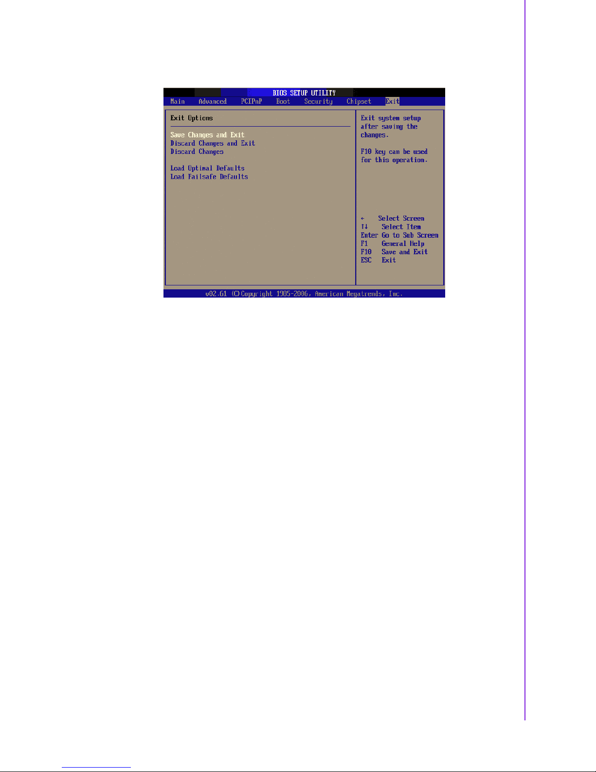
Figure 3.16 Exit Options
3.10.1 Save Changes and Exit
When you have completed system configuration, select this option to save your
changes, exit BIOS setup and reboot the computer so the new system configuration
parameters can take effect.
1. Select Save Changes and Exit from the Exit menu and press <Enter>. The fol-
lowing message appears:
Save Configuration Changes and Exit Now?
[Ok] [Cancel]
2. Select Ok or Cancel.
3.10.2 Discard Changes and Exit
Select this option to quit Setup without making any permanent changes to the system
configuration.
1. Select Discard Changes and Exit from the Exit menu and press <Enter>. The
following message appears:
Discard Changes and Exit Setup Now?
[Ok] [Cancel]
2. Select Ok to discard changes and exit.
3.10.3 Discard Changes
3. Select Discard Changes from the Exit menu and press <Enter>.
Page 55

PCA-6782 User Manual 44
3.10.4 Load Optimal Defaults
The PCA-6782 automatically configures all setup items to optimal settings when you
select this option. Optimal Defaults are designed for maximum system performance,
but may not work best for all computer applications. In particular, do not use the Optimal Defaults if your computer is experiencing system configuration problems. Select
Load Optimal Defaults from the Exit menu and press <Enter>.
3.10.5 Load Failsafe Defaults
The PCA-6782 automatically configures all setup options to failsafe settings when
you select this option. Failsafe Defaults are designed for maximum system stability,
but not maximum performance. Select Failsafe Defaults if your computer is experiencing system configuration problems.
1. Select Load Failsafe Defaults from the Exit menu and press <Enter>. The fol-
lowing message appears:
Load Failsafe Defaults?
[OK] [Cancel]
2. Select OK to load Failsafe defaults.
Page 56

Chapter 4
4 Value-Added Software
Services
Page 57
PCA-6782 User Manual 46
4.1 Value-Added Software Services
Software API: An interface that defines the ways in which an application program
may request services from libraries and/or operating systems. Provides not only the
underlying drivers required but also a rich set of user-friendly, intelligent and integrated interfaces, which speeds development, enhances security and offers add-on
value for
HPEHGGHG platforms. It plays the role of catalyst between developer and
solution, and ma
kes
embedded platforms easier and simpler to adopt andRSHUDWH
with customer applications.
4.1.1 Software API
4.1.1.1 Control
4.1.1.2 Display
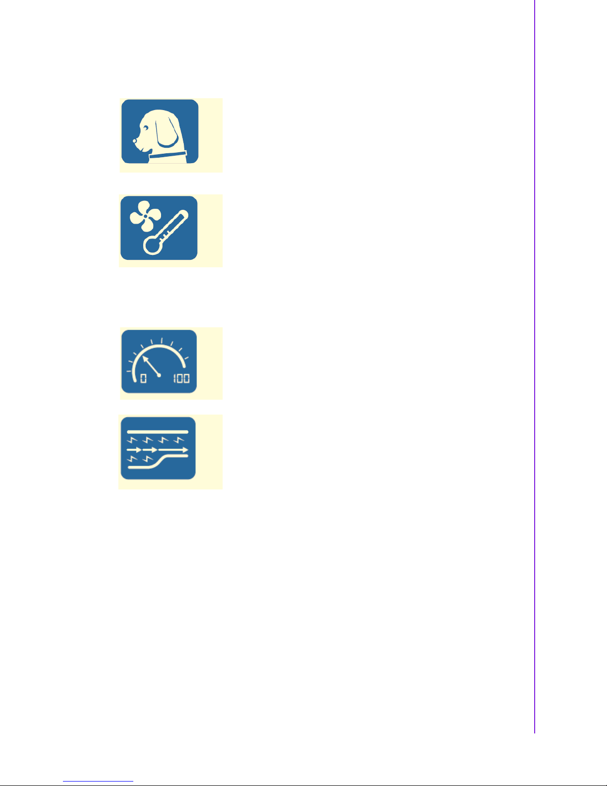
GPIO
General Purpose Input/Output is a flexible parallel interface
that allows a variety of custom connections. allows users to
monitor the level of signal input or set the output status to
switch on/off the device. Our API also provide Programmable
GPIO, allows developers to dynamically set the GPIO input
or output status.
Brightness Control
The Brightness Control API allows a developer to control
brightness easily on an embedded device.
Backlight
The Backlight API allows a developer to control the backlight
(screen) on/off on an embedded device.
Page 58
47 PCA-6782 User Manual
Chapter 4 Value-Added Software Services
4.1.1.3 Monitor
4.1.1.4 Power Saving
Watchdog
A watchdog timer (WDT) is a device that performs a specific
operation after a certain period of time if something goes
wrong and the system does not recover on its own. A watchdog timer can be programmed to perform a warm boot
(restarting the system) after a certain number of seconds.
Hardware Monitor
The Hardware Monitor (HWM) API is a system health supervision API that inspects certain condition indexes, such as
fan speed, temperature and voltage.
CPU Speed
Make use of Intel SpeedStep technology to reduce power
consumption. The system will automatically adjust the CPU
speed depending on the system loading.
System Throttling
Refers to a series of methods for reducing power consumption in computers by lowering the clock frequency. This API
allows the user to reduce the clock speed to 87.5% to 12.5%
of normal.
Page 59

PCA-6782 User Manual 48
4.1.2 Software Utility
BIOS Flash
The BIOS Flash utility allows customers to update the
flash ROM BIOS version, or use it to back up current BIOS
by copying it from the flash chip to a file on customers’
disk. The BIOS Flash utility also provides a command line
version and API for fast implementation into customized
applications.
Embedded Security ID
The embedded application is the most important property
of a system integrator. It contains valuable intellectual
property, design knowledge and innovation, but it is easily
copied! Embedded Security ID utility provides reliable
security functions for customers to secure their application
data within embedded BIOS.
Monitoring
Monitoring is a utility for customer to monitor the system
health, like voltage, CPU and system temperature and fan
speed. These items are important to a device; if the critical
errors happen and are not solved immediately, permanent
damage may be caused.
Flash Lock
Flash Lock is a mechanism to bind the Board and CF card
(SQFlash) together. User can “Lock” SQFlash via Flash
Lock function and “Unlock” by BIOS while booting. A locked
SQFlash cannot be read by any card reader or boot from
other platforms without a BIOS with an “Unlock” feature.
eSOS
(Requires BIOS Customization)
The eSOS is a small OS stored in BIOS ROM. It will boot up
in case of main OS crash. It will diagnose the hardware status, and then send an e-mail to administrator. The eSOS also
provide Remote Connection: Telnet server and FTP server
for administrator to rescue the system. Note: This function
requires BIOS customization.
Page 60

Chapter 5
5 Chipset Software
Installation Utility
Page 61

PCA-6782 User Manual 50
5.1 Before You Begin
To facilitate the installation of the enhanced display drivers and utility software, read
the instructions in this chapter carefully. The drivers for the PCA-6782 are located on
the software installation CD. The driver in the folder of the driver CD will guide and
link you to the utilities and drivers under a Windows system. Updates are provided
via Service Packs from Microsoft*.
Before you begin, it is important to note that most display drivers need to have the
relevant software application already installed in the system prior to installing the
enhanced display drivers. In addition, many of the installation procedures assume
that you are familiar with both the relevant software applications and operating system commands. Review the relevant operating system commands and the pertinent
sections of your application software’s user manual before performing the installation.
5.2 Introduction
The Intel® Chipset Software Installation (CSI) utility installs the Windows INF files
that outline to the operating system how the chipset components will be configured.
This is needed for the proper functioning of the following features:
! Core PCI PnP services
! IDE Ultra ATA 100/66/33 and Serial ATA interface support
! USB 1.1/2.0 support (USB 2.0 driver needs to be installed separately for Win98)
! Identification of Intel® chipset components in the Device Manager
! Integrates superior video features. These include filtered sealing of 720 pixel
DVD content, and MPEG-2 motion compensation for software DVD
Note! The files on the software installation CD are compressed. Do not
attempt to install the drivers by copying the files manually. You must use
the supplied SETUP program to install the drivers.
Page 62
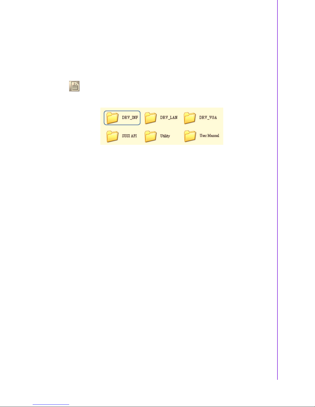
51 PCA-6782 User Manual
Chapter 5 Chipset Software Installation Utility
5.3 Windows 7/XP Driver Setup
1. Insert the driver CD into your system’s CD-ROM drive. You can see the driver
folder items. Navigate to the "DRV_INF" folder and click "infinst_autol.exe" to
complete the installation of the driver.
Note! Wrong driver installation may cause unexpected system instability.
Page 63

PCA-6782 User Manual 52
Page 64

Chapter 6
6 Integrated Graphic
Device Setup
Page 65
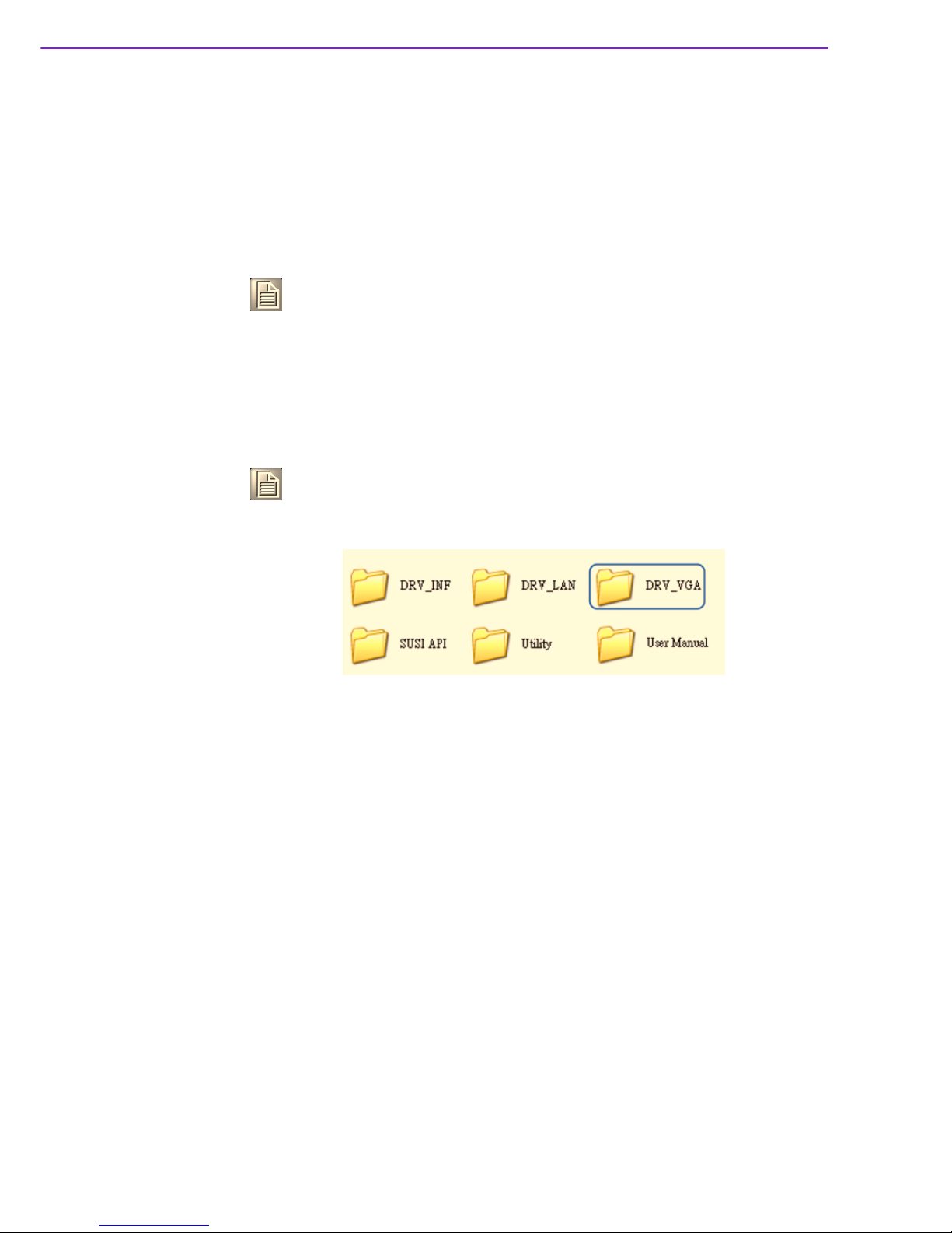
PCA-6782 User Manual 54
6.1 Introduction
To benefit from the Intel® Atom™ D525/N455 integrated graphics controller, you
need to install the graphic driver.
6.2 Windows 7/XP Driver Setup
Insert the driver CD into your system’s CD-ROM drive. You can see the driver folders
items. Navigate to the "DRV_VGA" folder and click "setup.exe" to complete the installation of the driver.
Note! Before installing this driver, make sure the CSI utility has been installed
in your system. See Chapter 4 for information on installing the CSI utility.
Note! Wrong driver installation may cause unexpected system instability.
Page 66

Chapter 7
7 LAN Configuration
Page 67
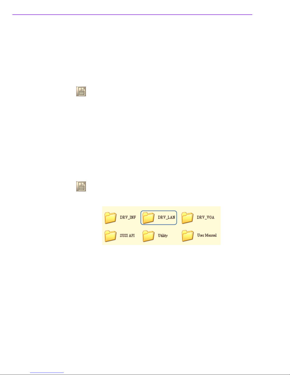
PCA-6782 User Manual 56
7.1 Introduction
The PCA-6782 has Signal Gigabit Ethernet LANs via dedicated PCI Express x1
lanes (Intel 82567V offers bandwidth of up to 500 MB/sec, eliminating the bottleneck
of network data flow and incorporating Gigabit Ethernet at 1000 Mbps).
7.2 Installation
The PCA-6782's Intel 82567V (LAN1) Gigabit integrated controllers support all major
network operating systems. However, the installation procedure varies from system
to system. Please find and use the section that provides the driver setup procedure
for the operating system you are using.
7.3 Windows 7/XP Driver Setup
Insert the driver CD into your system’s CD-ROM drive. Navigate to the "DRV_LAN"
folder and click "setup.exe" to complete the installation of the driver.
Note! Before installing the LAN drivers, make sure the CSI utility has been
installed on your system. See Chapter 4 for information on installing the
CSI utility.
Note! Wrong driver installation may cause unexpected system instability.
Page 68

Appendix A
A Programming the
Watchdog Timer
Page 69

PCA-6782 User Manual 58
A.1 Watchdog Timer
The PCA-6782's watchdog timer can be used to monitor system software operation
and take corrective action if the software fails to function after a programmed period.
This section describes the operation of the watchdog timer and how to program it.
A.1.1 Watchdog Timer Overview
The watchdog timer is built into the super I/O controller W83627DHG-P. It provides
the following functions for user programming:
! Can be enabled and disabled by user program.
! Timer can be set from 1 to 255 seconds or 1 to 255 minutes.
! Generates an interrupt or resets signal if the software fails to reset the timer
after time-out.
A.1.2 Reset/ Interrupt Selection
The JWDT1 jumper is used to trigger system reset signal or to change GPIO14 state
in the event the watchdog timer is tripped. See Chapter 1 for detailed jumper settings.
Page 70
59 PCA-6782 User Manual
Appendix A Programming the Watchdog Timer
A.1.3 Programming the Watchdog Timer
The I/O port address of the watchdog timer is 2E(hex) and 2F(hex).
2E (hex) is the address port. 2F(hex) is the data port.
You must first assign the address of the register by writing an address value into
address port 2E(hex), then write/read data to/from the assigned register through data
port 2F (hex).
Unlock W83627DHG-P
Select register of
watchdog timer
Enable watchdog
timer function
Use the function of
the watchdog timer
Lock W83627DHG-P
Page 71

PCA-6782 User Manual 60
Table A.1: Watchdog Timer Registers
Address of
register (2E)
Attribute
Read/Write Value (2F) and
description
87 (hex) ----- Write this address to I/O address port 2E (hex) twice to
unlock theW83627DHG-P
07 (hex) write Write 08 (hex) to select register of watchdog timer.
30 (hex) write Write 01 (hex) to enable the function of the watchdog
timer. Disabled is set as default.
F5 (hex) write Set seconds or minutes as units for the timer.
Write 0 to bit 3:
set second as
counting unit.
[default]
Write 1 to bit 3:
set minute as
counting unit
F6 (hex) write 0: stop timer [default] 01~FF (hex): The amount of the
count, in seconds or minutes, depends on the value set
in register F5 (hex). This number decides how long the
watchdog timer waits for strobe before generating an
interrupt or reset signal. Writing a new value to this register can reset the timer to count with the new value.
F7 (hex) read/write Bit 6: Write 1 to enable keyboard to reset the timer, 0 to
disable.[default]
Bit 5: Write 1 to generate a timeout signal immediately
and automatically return to 0. [default=0]
Bit 4: Read status of watchdog timer, 1 means timer is
""time out""."
AA (hex) ----- Write this address to I/O port 2E (hex) to lock the watch-
dog timer.2
Page 72

61 PCA-6782 User Manual
Appendix A Programming the Watchdog Timer
A.1.4 Example Program
1. Enable watchdog timer and set 10 sec. as timeout interval
;-------------------------------------------------------------------------------Mov dx,2e ; Unlock W83627DHG-P
Mov al,87h
Out dx,al
Out dx,al
;--------------------------------------------------------------------------------
Mov al,07h ; Select registers of watchdog timer
Out dx,al
Inc dx
Mov al,08h
Out dx,al
;--------------------------------------------------------------------------------
Dec dx ; Enable the function of watchdog timer
Mov al,30h
Out dx,al
Inc dx
Mov al,01h
Out dx,al
;--------------------------------------------------------------------------------
Dec dx ; Set second as counting unit
Mov al,0f5h
Out dx,al
Inc dx
In al,dx
And al,not 08h
Out dx,al
;--------------------------------------------------------------------------------
Dec dx ; Set timeout interval as 10 seconds and start counting
Mov al,0f6h
Out dx,al
Inc dx
Mov al,10
Out dx,al
;--------------------------------------------------------------------------------
Dec dx ; lock W83627DHG-P
Mov al,0aah
Out dx,al
2. Enable watchdog timer and set 5 minutes as timeout interval
;--------------------------------------------------------------------------------
Mov dx,2eh ; unlock W83627DHG-P
Mov al,87h
Out dx,al
Out dx,al
Page 73

PCA-6782 User Manual 62
;-------------------------------------------------------------------------------Mov al,07h ; Select registers of watchdog timer
Out dx,al
Inc dx
Mov al,08h
Out dx,al
;-------------------------------------------------------------------------------Dec dx ; Enable the function of watchdog timer
Mov al,30h
Out dx,al
Inc dx
Mov al,01h
Out dx,al
;--------------------------------------------------------------------------------
Dec dx ; Set minute as counting unit
Mov al,0f5h
Out dx,al
Inc dx
In al,dx
Or al,08h
Out dx,al
;--------------------------------------------------------------------------------
Dec dx ; Set timeout interval as 5 minutes and start counting
Mov al,0f6h
Out dx,al
Inc dx
Mov al,5
Out dx,al
;-------------------------------------------------------------------------------Dec dx ; lock W83627DHG-P
Mov al,0aah
Out dx,al
3. Enable watchdog timer to be reset by mouse
;--------------------------------------------------------------------------------
Mov dx,2eh ; unlock W83627DHG-P
Mov al,87h
Out dx,al
Out dx,al
;--------------------------------------------------------------------------------
Mov al,07h ; Select registers of watchdog timer
Out dx,al
Inc dx
Mov al,08h
Out dx,al
;--------------------------------------------------------------------------------
Page 74

63 PCA-6782 User Manual
Appendix A Programming the Watchdog Timer
Dec dx ; Enable the function of watchdog timer
Mov al,30h
Out dx,al
Inc dx
Mov al,01h
Out dx,al
;-------------------------------------------------------------------------------Dec dx ; Enable watchdog timer to be reset by mouse
Mov al,0f7h
Out dx,al
Inc dx
In al,dx
Or al,80h
Out dx,al
;--------------------------------------------------------------------------------
Dec dx ; lock W83627DHG-P
Mov al,0aah
Out dx,al
4. Enable watchdog timer to be reset by keyboard
;--------------------------------------------------------------------------------
Mov dx,2eh ; unlock W83627DHG-P
Mov al,87h
Out dx,al
Out dx,al
;--------------------------------------------------------------------------------
Mov al,07h ; Select registers of watchdog timer
Out dx,al
Inc dx
Mov al,08h
Out dx,al
;--------------------------------------------------------------------------------
Dec dx ; Enable the function of watchdog timer
Mov al,30h
Out dx,al
Inc dx
Mov al,01h
Out dx,al
;-------------------------------------------------------------------------------Dec dx ; Enable watchdog timer to be strobed reset by keyboard
Mov al,0f7h
Out dx,al
Inc dx
In al,dx
Or al,40h
Out dx,al
Page 75

PCA-6782 User Manual 64
;-------------------------------------------------------------------------------Dec dx ; lock W83627DHG-P
Mov al,0aah
Out dx,al
5. Generate a time-out signal without timer counting
;--------------------------------------------------------------------------------
Mov dx,2eh ; unlock W83627DHG-P
Mov al,87h
Out dx,al
Out dx,al
;--------------------------------------------------------------------------------
Mov al,07h ; Select registers of watchdog timer
Out dx,al
Inc dx
Mov al,08h
Out dx,al
;--------------------------------------------------------------------------------
Dec dx ; Enable the function of watchdog timer
Mov al,30h
Out dx,al
Inc dx
Mov al,01h
Out dx,al
;--------------------------------------------------------------------------------
Dec dx ; Generate a time-out signal
Mov al,0f7h
Out dx,al ;Write 1 to bit 5 of F7 register
Inc dx
In al,dx
Or al,20h
Out dx,al
;-------------------------------------------------------------------------------Dec dx ; lock W83627DHG-P
Mov al,0aah
Out dx,al
Page 76

Appendix B
B I/O Pin Assignments
Page 77
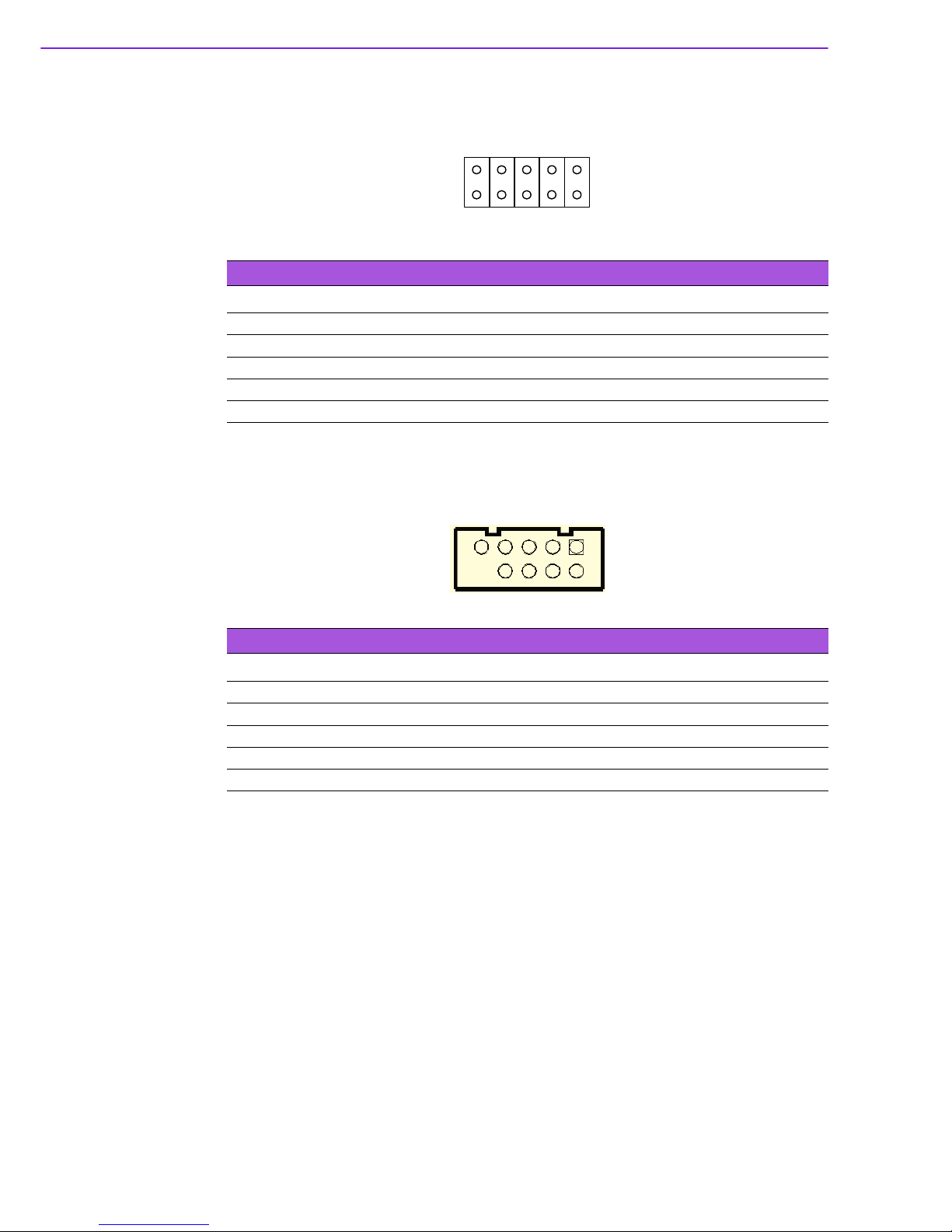
PCA-6782 User Manual 66
B.1 Front Panel Connectors (JFP1)
B.2 USB Ports (USB12/USB34/USB56/USB78)
Table B.1: Front Panel Connectors (JFP1)
Pin Signal Pin Signal
1 VCC3 2 HDD LED
3 VCC3 4 Power LED
5 5 VSB 6 Suspend LED
7 System Reset Button 8 GND
9 ATX Power Button 10 GND
2436810
5791
Table B.2: USB Ports (USB12/USB34/USB56/USB78)
Pin Signal Pin Signal
1VCC 2VCC
3 USB Data1- 4 USB Data2-
5 USB Data1+ 6 USB Data2+
7GND 8GND
9NC 10
Page 78
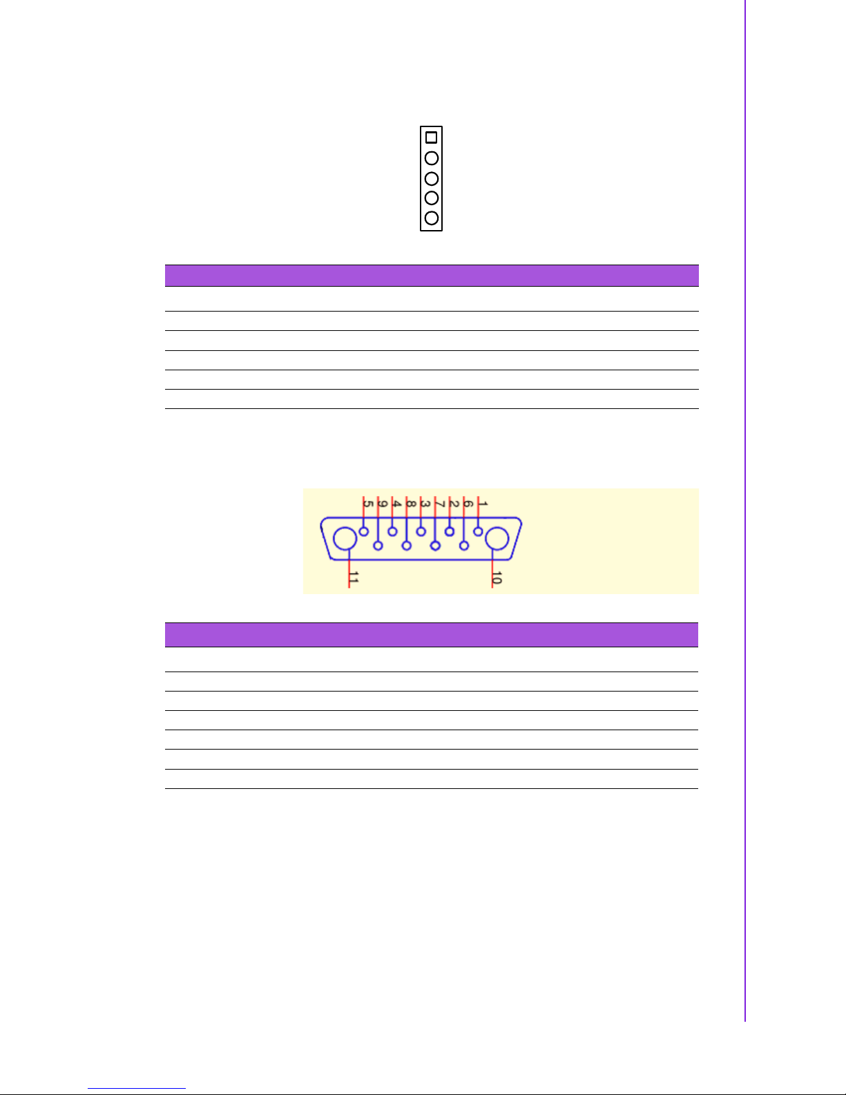
67 PCA-6782 User Manual
Appendix B I/O Pin Assignments
B.3 IR Connector (JIR1)
B.4 Serial port (COM1)
Table B.3: IR Connector (JIR1)
Pin Signal
1VCC
2NC
3 IR_RX
4GND
5IR_TX
1
5
2
3
4
Table B.4: Serial port (COM1)
Pin Signal Pin Signal
1 DCD 2 SIN
3 SOUT 4 DTR
5 GND 6 DSR
7 RTSA 8 CTS
9 RIA 10 GND
11 GN D
Page 79
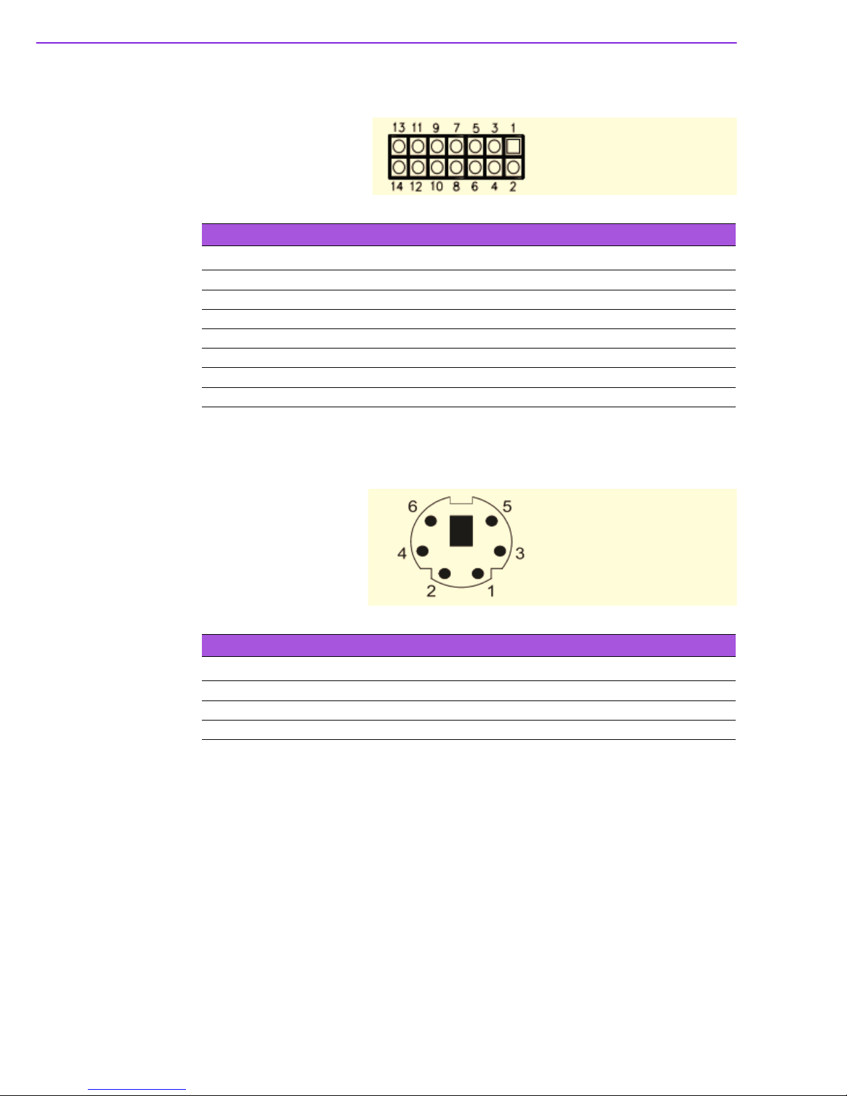
PCA-6782 User Manual 68
B.5 Serial port (COM2)
B.6 PS/2 keyboard and mouse connector (KBMS1)
Table B.5: Serial port (COM2)
Pin Signal Pin Signal
1DCD 2 DSR
3 SIN 4 RTS
5 SOUT 6 CTS
7 DTR 8 RI
9 GND 10 GND
11 NC 12 NC
13 NC 14 NC
Table B.6: PS/2 keyboard and mouse connector (KBMS1)
Pin Signal Pin Signal
1 PS2 keyboard data 2 PS2 mouse data
3 GND 4 VCC
5 PS2 keyboard clock 6 PS2 mouse clock
Page 80
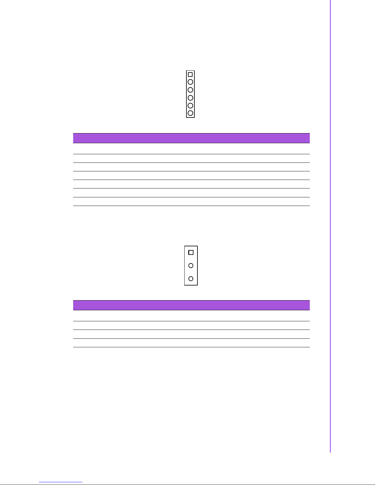
69 PCA-6782 User Manual
Appendix B I/O Pin Assignments
B.7 External keyboard and mouse connector
(KBMS2)
B.8 ATX Feature connector(ATXF1)
Table B.7: External keyboard and mouse connector (KBMS2)
Pin Signal
1 PS2 keyboard clock
2 PS2 keyboard data
3 PS2 mouse data
4GND
5VCC
6 PS2 mouse clock
6
1
Table B.8: ATX Feature connector(ATXF1)
Pin Signal
1 5V standby
2VCC
3 PS_ON#
1
2
3
Page 81
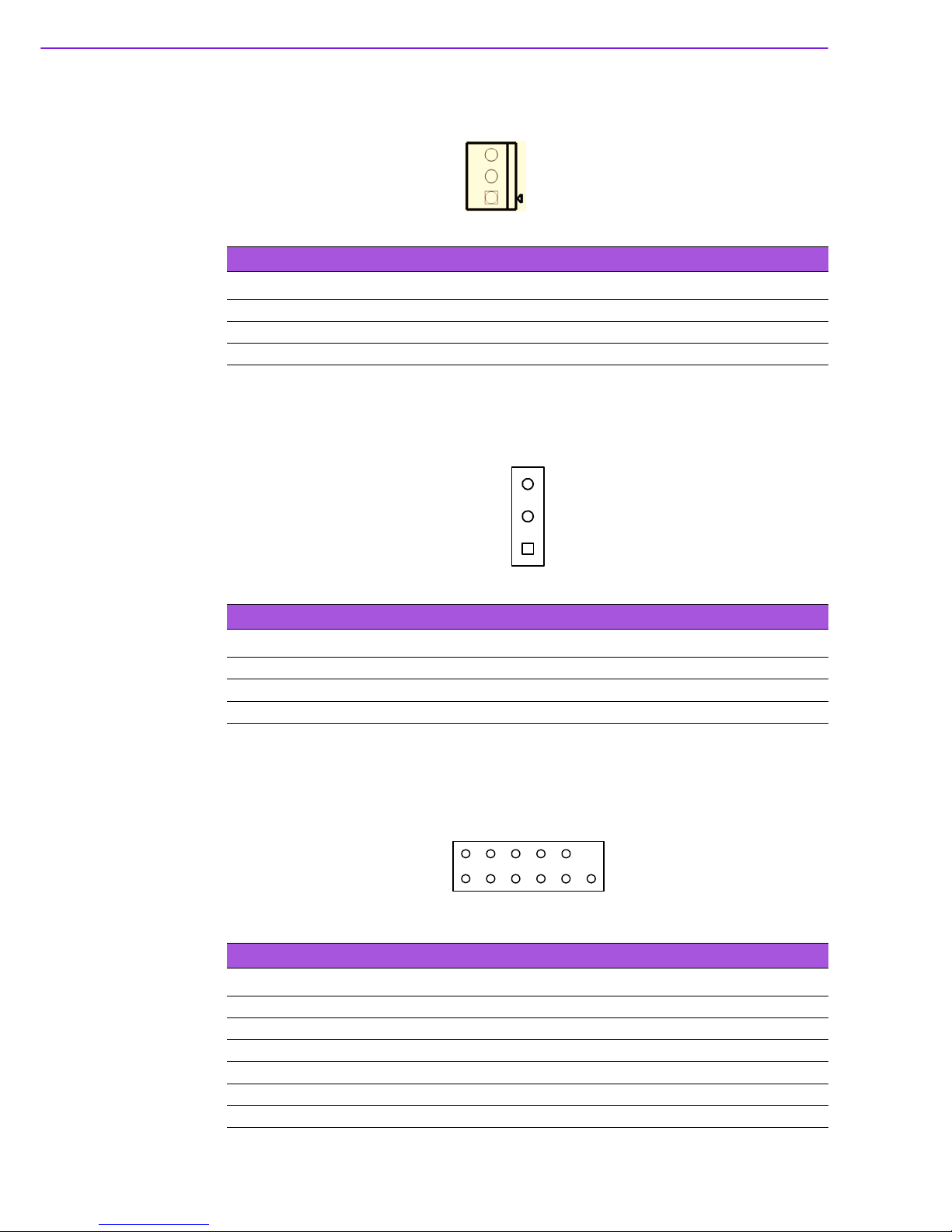
PCA-6782 User Manual 70
B.9 CPU FAN connector (CPUFAN1)
B.10 System FAN connector (SYSFAN1)
B.11 Audio Interface Connector (HDAUD1)
Table B.9: CPU FAN connector (CPUFAN1)
Pin Signal
1GND
2 +12V
3 FAN_TACH
3
2
1
Table B.10: System FAN connector (SYSFAN1)
Pin Signal
1GND
2 +12V
3 FAN_TACH
3
2
1
Table B.11: Audio Interface Connector (HDAUD1)
Pin Signal Pin Signal
1 ACZ_VCC 2 GND
3 ACZ_SYNC 4 ACZ_BITCLK
5 ACZ_SDOUT 6 ACZ_SDIN0
7 ACZ_SDIN1 8 ACZ_RST#
9 ACZ_12V 10 GND
11 GN D 1 2
2436810
5791
11
Page 82
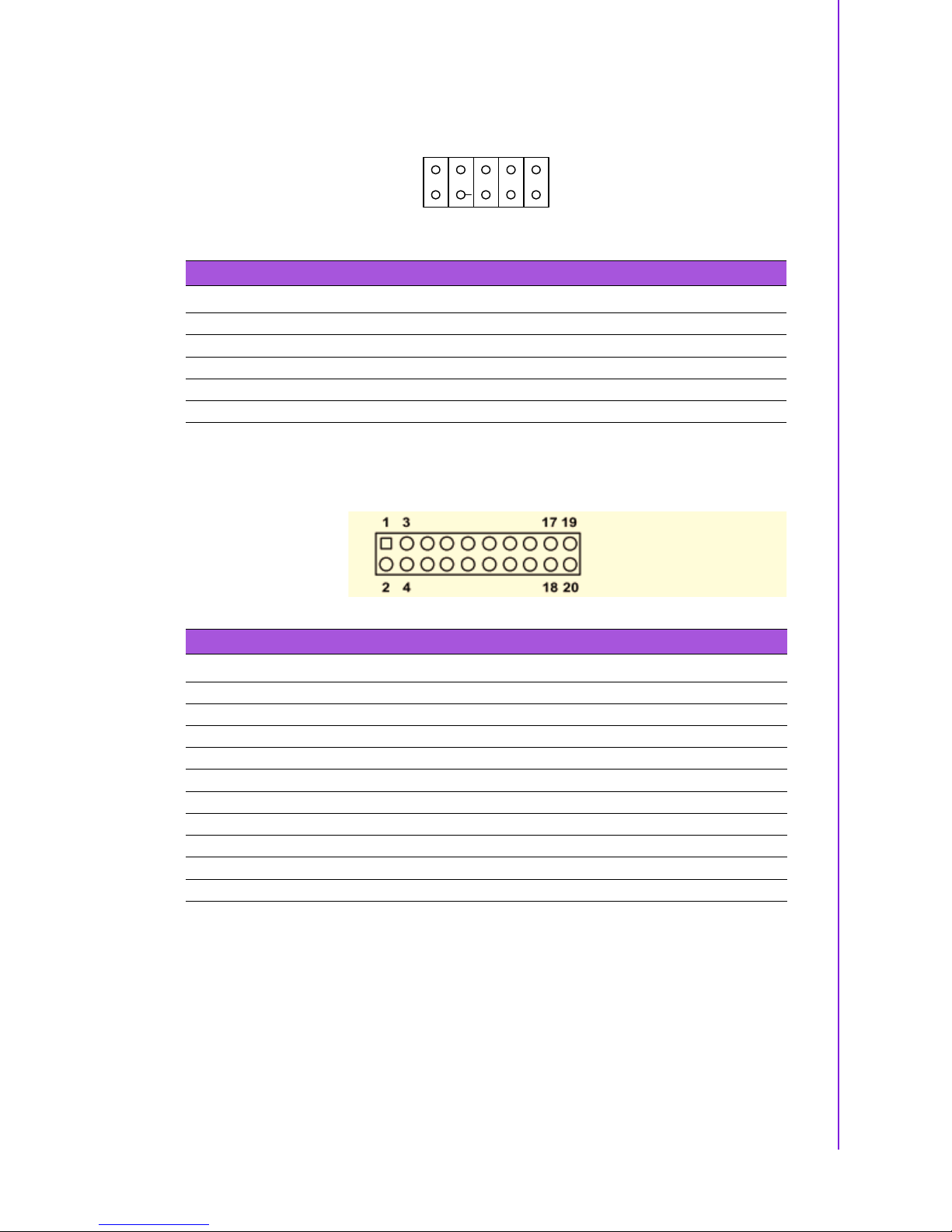
71 PCA-6782 User Manual
Appendix B I/O Pin Assignments
B.12 GPIO Header (GPIO1)
B.13 LVDS Connector (LVDS1)
Table B.12: GPIO Header (GPIO1)
Pin Signal Pin Signal
1 GPIO1 2 GPIO5
3 GPIO2 4 GPIO6
5 GPIO3 6 GPIO7
7 GPIO4 8 GPIO8
9VCC 10GND
2436810
5791
Table B.13: LVDS Connector (LVDS1)
Pin Signal Pin Signal
1 GND 2 GND
3 NC 4 LVDS0_D0+
5 NC 6 LVDS0_D0-
7 NC 8 LVDS0_D1+
9 NC 10 LVDS0_D1-
11 NC 12 LVDS0_D2+
13 NC 14 LVDS0_D2-
15 NC 16 LVDS0_CLK+
17 NC 18 LVDS0_CLK-
19 LVDS power 20 LVDS power
Page 83
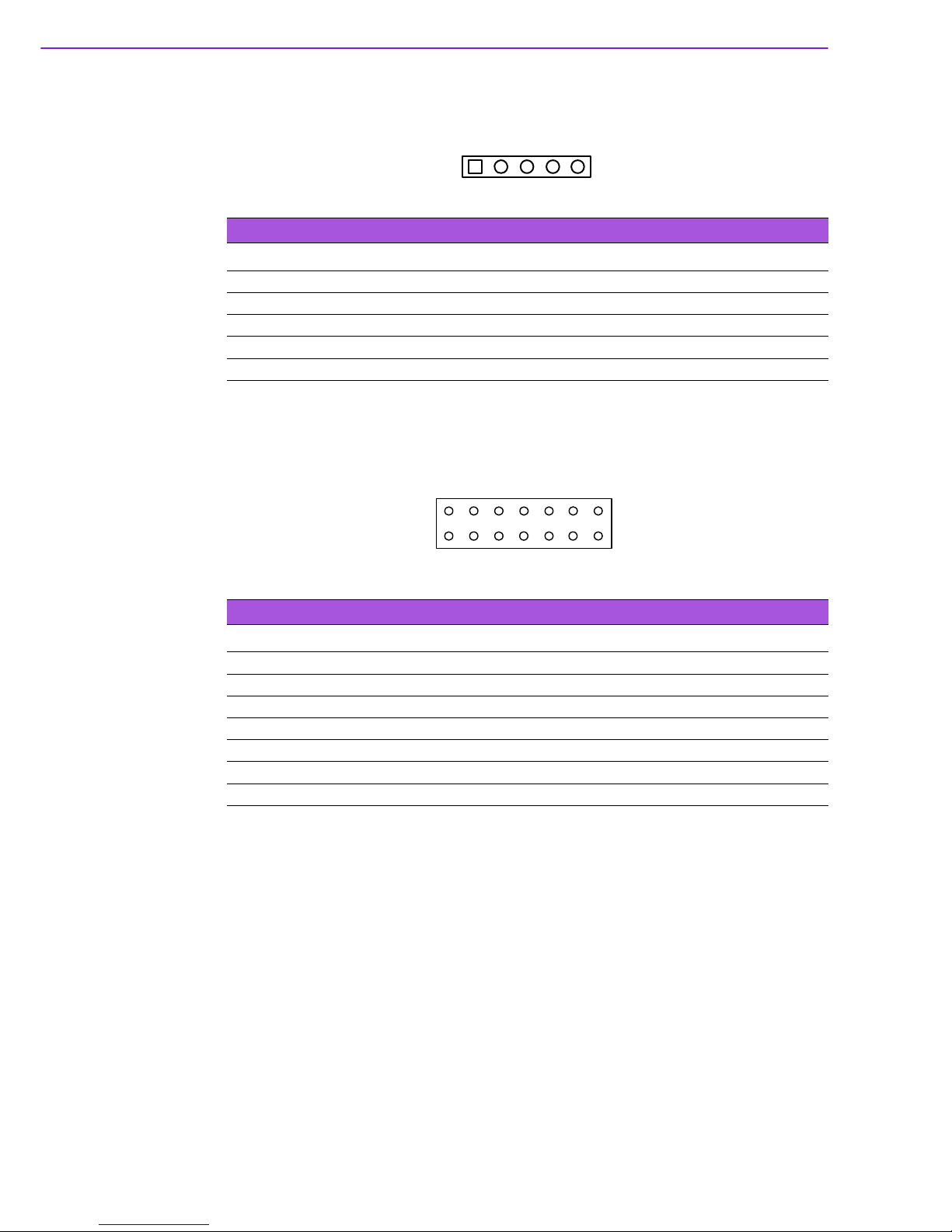
PCA-6782 User Manual 72
B.14 LCD Inverter Connector (INV1)
B.15 Low Pin Count Header (LPC1)
Table B.14: LCD Inverter Connector (INV1)
Pin Signal
1 +12V
2GND
3 Back-light enable signal output
4 Back-light VBR signal output
5VCC
12 43 5
Table B.15: Low Pin Count Header (LPC1)
Pin Signal Pin Signal
1 LPC_HEADER 2 LPC_LAD1
3 LPC_RST# 4 LPC_LAD0
5LPC_FRAME#6 +3.3V
7LPC_LAD3 8 GND
9 LPC_LAD2 10 LPC_LDRQ1#
11 SERIRQ 12 PWROK
13 5V Standby 14 +5V
2436810
5791
11 13
12 14
Page 84
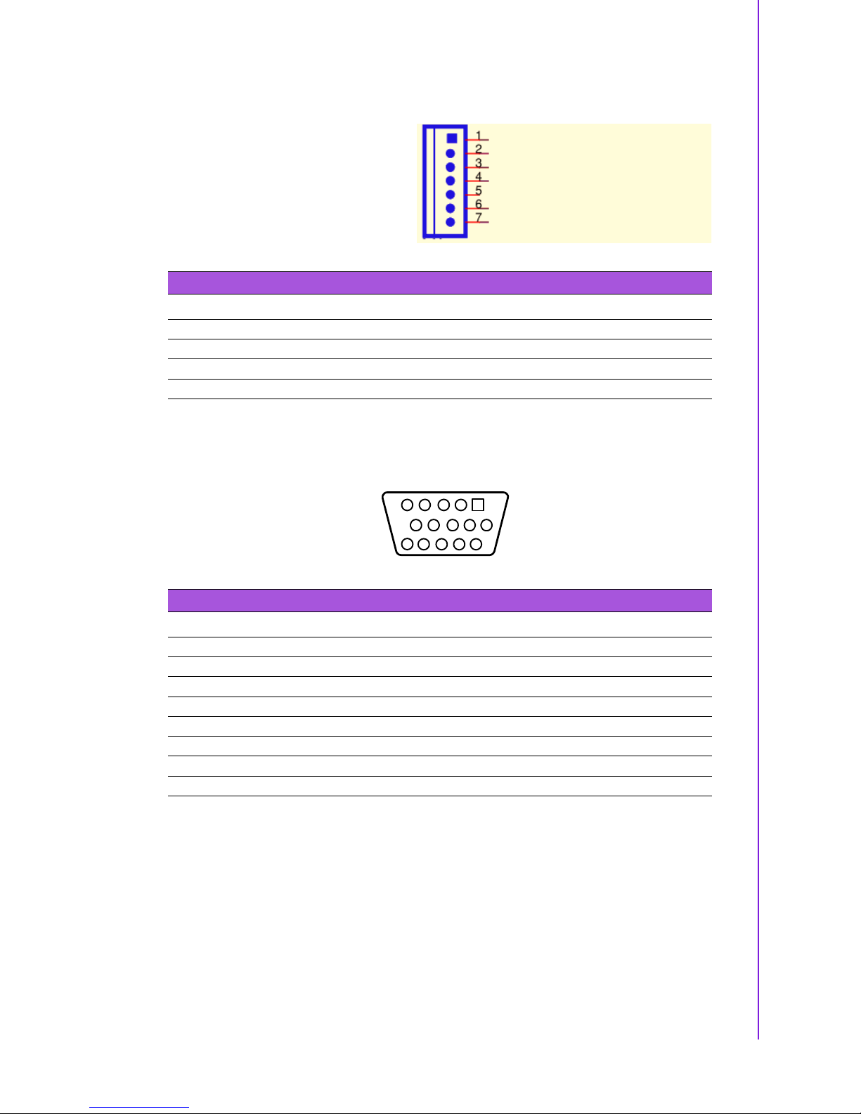
73 PCA-6782 User Manual
Appendix B I/O Pin Assignments
B.16 ATX Power Control Connector (ATX1)
B.17 VGA Connector (VGA1)
Table B.16: ATX Power Control Connector (ATX1)
Pin Signal Pin Signal
1+5V 2GND
3 GND 4 +12V
5 NC 6 GND
7 +5V
Table B.17: VGA Connector (VGA1)
Pin Signal Pin Signal
1 VGA_R 2 VGA_G
3 VGA_B 4 NC
5 GND 6 GND
7 GND 8 GND
9 CRT_VCCIN 10 GND
11 NC 12 V_SDAT
13 H-SYNC 14 V-SYNC
15 V_SCLK
5
15
1
11
10 6
Page 85
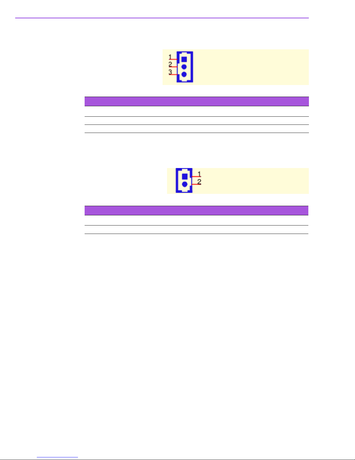
PCA-6782 User Manual 74
B.18 Negative power input connector (12V1)
B.19 Case open (JCASE1)
Table B.18: Negative power input connector (12V1)
Pin Signal Pin Signal
1-5V 2GND
3 -12V
Table B.19: Case open (JCASE1)
Pin Signal Pin Signal
1 CASEOP# 2 GND
Page 86
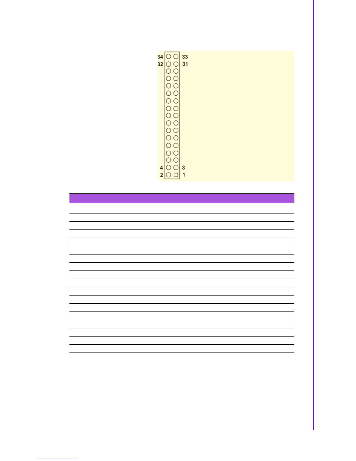
75 PCA-6782 User Manual
Appendix B I/O Pin Assignments
B.20 FDD connector (FDD1)
Table B.20: FDD connector (FDD1)
Pin Signal Pin Signal
1GND 2DRVEN0
3 GND 4 NC
5 NC 6 NC
7 GND 8 INDEX#
9 GND 10 MOA#
11 GN D 12 NC
13 GND 14 DSA#
15 GND 16 NC
17 GND 18 DIR#
19 GND 20 STEP#
21 GND 22 WD#
23 GND 24 WE#
25 GND 26 TRAK0#
27 GND 28 WP#
29 GND 30 RDATA#
31 GND 32 HEAD#
33 GND 34 DSKCHG#
Page 87
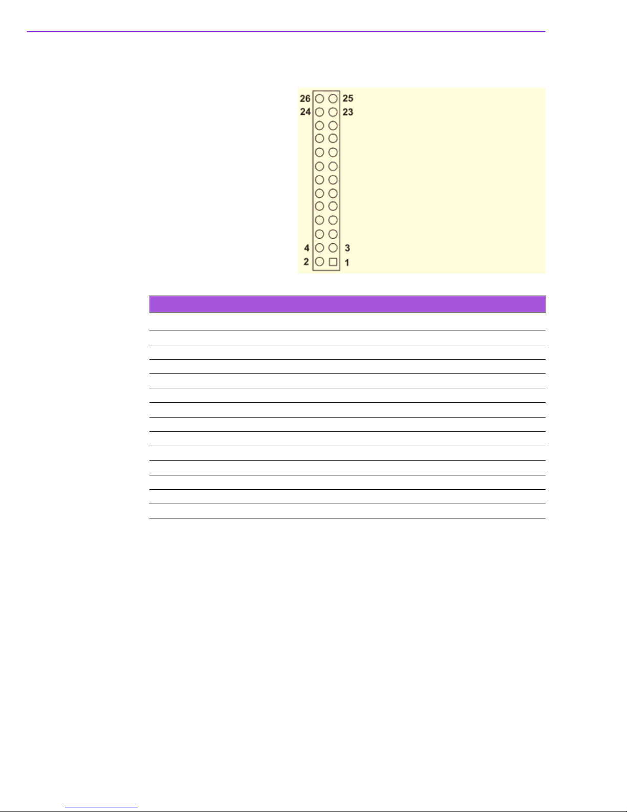
PCA-6782 User Manual 76
B.21 Parallel port connector (LPT1)
Table B.21: Parallel port connector (LPT1)
Pin Signal Pin Signal
1STB# 2AFD#
3 D0 4 ERR#
5 D1 6 INIT#
7 D2 8 SLIN
9 D3 10 GND
11 D4 12 GN D
13 D5 14 GND
15 D6 16 GND
17 D7 18 GND
19 ACK# 20 GND
21 BUSY 22 GND
23 PE 24 GND
25 SLCT 26 NC
Page 88
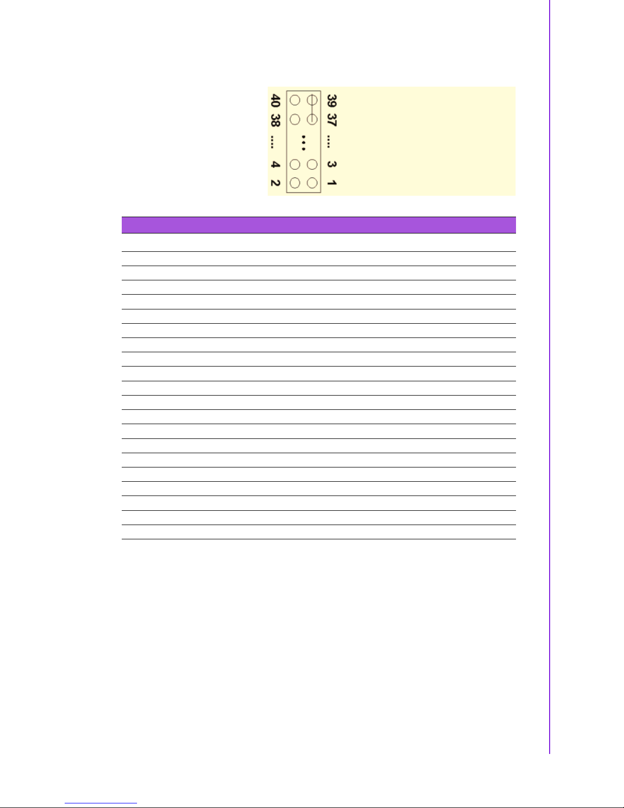
77 PCA-6782 User Manual
Appendix B I/O Pin Assignments
B.22 IDE connector (IDE1)
Table B.22: IDE connector (IDE1)
Pin Signal Pin Sign al
1 IDE RESET 2 GND
3 D7 4 D8
5 D6 6 D9
7 D5 8 D10
9 D4 10 D11
11 D3 12 D12
13 D2 14 D13
15 D1 16 D14
17 D0 18 D15
19 GND 20 NC
21 REQ 22 GND
23 IOW 24 GND
25 IOR 26 GND
27 READY 28 Cable Select
29 DACK 30 GND
31 IRQ14 32 NC
33 A1 34 ATA check
35 A0 36 A2
37 CS1# 38 CS3#
39 LED 40 GND
Page 89
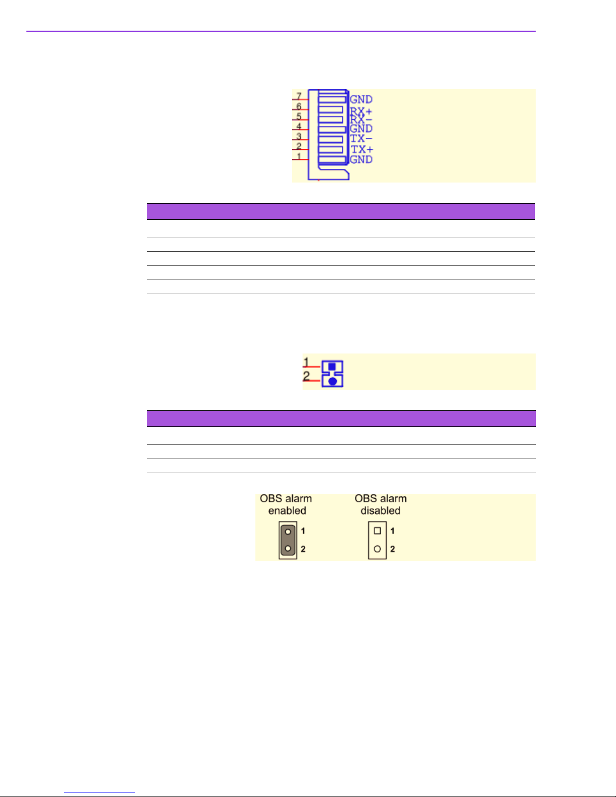
PCA-6782 User Manual 78
B.23 Serial ATA (SATA1/SATA2/SATA3)
B.24 HW Monitor Alarm (JOBS1)
Table B.23: Serial ATA (SATA1/SATA2/SATA3)
Pin Signal Pin Signal
1GND 2SATA TX+
3 SATA TX- 4 GND
5 SATA RX- 6 SATA RX+
7 GND
Table B.24: Serial ATA (SATA1/SATA2/SATA3)
Setting Function
1-2 Closed Enable OBS alarm
1-2 Open Disable OBS alarm
Page 90
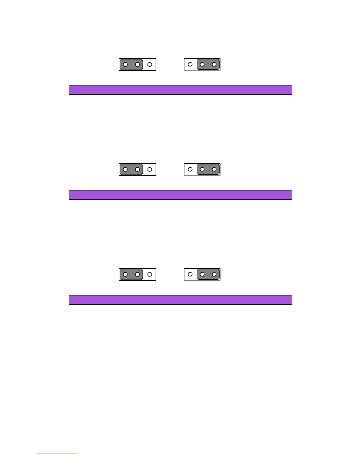
79 PCA-6782 User Manual
Appendix B I/O Pin Assignments
B.25 LVDS VBR selection (JVBR1)
B.26 LVDS panel power selection (JLVDS1)
B.27 Watchdog timer output selection (JWDT1)
Table B.25: LVDS VBR selection (JVBR1)
Ping Function
1-2 (default) Linear way to control brightness*
2-3 PWM to control brightness
123
1 23
Table B.26: LVDS panel power selection (JLVDS1)
Ping Function
1-2 (default) +3.3 V
2-3 +5 V
123
1 23
Table B.27: Watchdog timer output selection (JWDT1)
Ping Function
1-2 IRQ11
2-3 (default) System Reset
123
1 23
Page 91
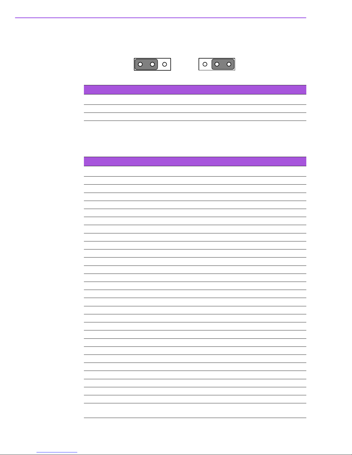
PCA-6782 User Manual 80
B.28 CMOS clear (CMOS1)
B.29 System I/O Ports
Table B.28: CMOS clear (CMOS1)
Ping Function
1-2 (default) Keep CMOS data
2-3 Clear CMOS data
123
1 23
Table B.29: System I/O ports
Addr. range (Hex) Device
000-008h DMA controller
09h-0Eh RESERVED
0Fh-18h DMA Controller
19h-1Eh RESERVED
1Fh DMA Controller
20h-2Dh Interrupt Controller
2E-2F LPC SIO
30h-3Dh Interrupt Controller
40h-42h Timer/Counter
43h RESERVED
4E-4F LPC SIO
50h-52h Timer/Counter
53h RESERVED
60h Microcontroller
61h NMI Controller
62h-66h Microcontroller
70h RESERVED
71h-77h RTC Controller
80h- 91h DMA Controller,
92h Reset Generator
93h-9Fh DMA Controller
A0h-B1h Interrupt Controller
B2h-B3h Power Management
B4h-BDh Interrupt Controller
C0h-D1h DMA Controller
D2h-DDh RESERVED
DEh-DFh DMA Controller
F0h PCI and Master Abort
170h-3F6h
IDE Controller (Mobile only),
SATA Controller, or PCI
Page 92

81 PCA-6782 User Manual
Appendix B I/O Pin Assignments
B.30 DMA Channel Assignments
B.31 Interrupt Assignments
4D0h-4D1h Interrupt Controller
CF9h Reset Generator
290h-29Fh H/W monitor
C80h-CBFh Additional Serial I/O module
Table B.29: System I/O ports
Table B.30: DMA channel assignments
Channel Function
0 Available
1 Available
2 Floppy disk (8-bit transfer)
3 Available
4 Cascade for DMA controller 1
5 Available
6 Available
7 Available
Table B.31: Interrupt assignments
Priority Interrupt# Interrupt source
1 NMI Parity error detected
2 IRQ0 Interval timer
3 IRQ1 Keyboard
- IRQ2 Interrupt from controller 2 (cascade)
4 IRQ8 Real-time clock
5 IRQ9 Cascaded to INT 0A (IRQ 2)
6 IRQ10 Available/Serial communication port 3, 4, 5, 6
7 IRQ11 Available
8 IRQ12 PS/2 mouse
9 IRQ13 INT from co-processor
10 IRQ14 Primary IDE Channel
11 IRQ15 Secondary IDE Channel
12 IRQ3 Serial communication port 2
13 IRQ4 Serial communication port 1
14 IRQ5 Available
15 IRQ6 Diskette controller (FDC)
16 IRQ7 Parallel port 1 (print port)
Page 93

PCA-6782 User Manual 82
B.32 1st MB Memory Map
Table B.32: 1st MB memory map
Addr. range (Hex) Device
E0000h - FFFFFh BIOS
CC000h - DFFFFh Unused
C0000h - CDFFFh VGA BIOS
A0000h - BFFFFh Video Memory
00000h - 9FFFFh Base memory
Page 94

Appendix C
C Programming the
GPIO
Page 95

PCA-6782 User Manual 84
C.1 Supported GPIO Register
Bellow are detailed description of the GPIO addresses and programming sample.
C.1.1 GPIO Registers
Extended Function Index Registers (EFIRs)
The EFIRs are write-only registers with port address 2Eh on PC/AT systems.
Extended Function Data Registers(EFDRs)
The EFDRs are read/write registers with port address 2Fh on PC/AT systems.
CR07 (Logical Device Number Register)
Set to ‘09’ to modify GPIO settings.
CRF0 (GP10-GP17 I/O selection register. Default 0xFF)
When set to '1', the respective GPIO port is programmed as an input port.
When set to '0', the respective GPIO port is programmed as an output port.
CRF1 (GP10-GP17 data register. Default 0x00)
If a port is programmed to be an output port, then its respective bit can be read/written.
If a port is programmed to be an input port, then its respective bit can only be read.
CRF2 (GP10-GP17 inversion register. Default 0x00)
When set to '1', the incoming/outgoing port value is inverted.
When set to '0', the incoming/outgoing port value is the same as in data register.
Page 96

85 PCA-6782 User Manual
Appendix C Programming the GPIO
C.1.2 GPIO Example Program-1
------------------------------------------------------------
Enter the extended function mode, interruptible double-write
------------------------------------------------------------
MOV DX, 2Eh
MOV AL, 87h
OUT DX, AL
OUT DX, AL
------------------------------------------------------------
Configure logical device 7(GP10~GP17), configuration register CRF0,CRF1,CRF2
------------------------------------------------------------
MOV DX, 2Eh
MOV AL, 07h; point to Logical Device Number Reg.
OUT DX, AL
MOV DX, 2Fh
MOV AL, 07h; select logical device 7
OUT DX, AL
MOV DX, 2Eh
MOV AL, F0h
OUT DX, AL
MOV DX, 2Fh
MOV AL, 00h; 01: Input, 00: output for GP10~GP17
OUT DX, AL
MOV DX, 2Eh
MOV AL, F2h ;
OUT DX, AL
MOV DX, 2Fh
MOV AL, 00h; Set GPIO is normal not inverter
OUT DX, AL;
MOV DX, 2Eh
MOV AL, F1h
OUT DX, AL
MOV DX, 2Fh
MOV AL, ??h; Put the output value into AL
OUT DX, AL
------------------------------------------------------------
Exit extended function mode |
------------------------------------------------------------
MOV DX, 2Eh
MOV AL, AAh
OUT DX, AL
 Loading...