

Page 1

2390 EMAC, Way
Carbondale, IL 62902
Phone: (618) 529-4525
Fax: (618) 457-0110
http://www.emacinc.com
iPac HCS12
Users Manual
Copyright 2003
EMAC, Inc.
Page 2

iPac HCS12 Users Manual rev1.2
Copyright EMAC. Inc. 2003
Table of Contents
1. Introduction..........................................................................................................................................................................2
1.1 Features........................................................................................................................................................................2
1.2 Options.........................................................................................................................................................................2
1.3 Other Options...............................................................................................................................................................3
2. Hardware..............................................................................................................................................................................3
2.1 Specifications...............................................................................................................................................................3
2.2 Jumpers........................................................................................................................................................................3
2.3 JTAG & BDM..............................................................................................................................................................4
2.4 Processor Based Multi-Purpose Digital I/O.................................................................................................................5
2.5 PLD Based General Purpose Digital I/O......................................................................................................................6
2.6 Analog Channels..........................................................................................................................................................7
2.7 RS232 SERIAL 0 UART.............................................................................................................................................8
2.8 RS 232/422/485 SERIAL 1 UART..............................................................................................................................8
2.9 CAN I/O.......................................................................................................................................................................9
2.10 LCD .............................................................................................................................................................................9
2.11 Keypad.......................................................................................................................................................................10
2.12 Real Time Clock (RTC).............................................................................................................................................10
3. Software.............................................................................................................................................................................11
3.1 Introduction ................................................................................................................................................................11
3.2 Bootloader..................................................................................................................................................................11
4. PCD-39E00 Terminal Board..............................................................................................................................................12
4.1 Introduction................................................................................................................................................................12
4.2 iPac Terminal Board Pinout.......................................................................................................................................12
This document is the ownership of EMAC, Inc. Copyright 2003. Unauthorized duplication or copying of this document is strictly forbidden.
iPac HCS12 Manual.doc - 1 - Rev 1.2 - 11/11/03
Page 3

1. Introduction
This document describes EMAC’s iPac HCS12 Single Board Computer (SBC) module. The iPac HCS12 is a PC/104 SBC
sized module that provides a wide variety of I/O. Controlled by Motorola’s powerful HCS12 processor this module provides
maximum flexibility with ample processing speed for most control applications. Although being extremely powerful with
ample I/O for demanding applications, this board consumes minimal power, is low cost, and has a small footprint. The iPac
HCS12 uses the Standard PC/104 form factor (3.8" x 3.5") allowing the use of standard PC/104 mounting hardware and
enclosures. The features of the iPac HCS12 are as follows:
1.1 Features
§ CPU: Motorola 68HCS12 16 Bit Processor running with a CPU clock speed of about 50 MHz with BDM debugger
capability.
§ MEMORY: 128K of internal Flash in-circuit programmable, 2K byte EEPROM, 8K of RAM, and 96 bytes of
battery backed RAM.
§ DIGITAL I/O: 16 General Purpose HCS12 Digital I/O lines, 8 Digital Inputs, 8 Digital Outputs, and 8 High Drive
Digital Outputs..
§ COUNTER/PWM: 8 Multi-Purpose HCS12 Digital I/O lines (GP/Counters/PWM).
§ ANALOG INPUTS: 16 channels of 10 bit A/D 0 - 5 volts.
§ ANALOG OUTPUTS: 2 channels of 8 bit D/A using filtered PWM channels.
§ COMMUNICATION: 1 RS232 Port and 1 RS232/422/485 port.
§ TIME: Battery Backed Real Time Clock/Calendar.
§ RESET: External Reset Button provision.
§ INTERFACES: Character LCD interface with backlight support and a 24 key, keypad interface.
• FORM FACTOR: PC/104 Module with Dimensions of 96 mm x 90 mm (3.77" x 3.54").
1.2 Options
ON-BOARD OPTIONS
• ANALOG: Analog I/O Upgrade Includes:
• 8 additional channels of 12 bit A/D, 0 - 5 Volts or 4 to 20 ma. input provision.
• 4 additional channels of 12 bit D/A, 0 - 5 Volts.
• CAN: An Optically Isolated CAN 2.0 A, B Port.
• SOFTWARE: MODBUS slave capability.
This document is the ownership of EMAC, Inc. Copyright 2003. Unauthorized duplication or copying of this document is strictly forbidden.
iPac HCS12 Manual.doc - 2 - Rev 1.2 - 11/11/03
Page 4

1.3 Other Options
• TERMINAL BOARD: Screw Terminal Board allows for easy access to the iPac HCS12 I/O. Up to two Screw
Terminal Boards can be stacked onto a single iPac HCS12.
2. Hardware
2.1 Specifications
§ VOLTAGE REQUIREMENTS: Onboard regulation allows 5 volt or 7.5 - 15 volt DC board input voltage.
§ CURRENT REQUIREMENTS: 120 ma. @ 5 Volts Typical
§ OPERATING TEMPERATURE: 0 - 70 degrees Centigrade, humidity range without condensation 0% to 90%
RH.
§ DIGITAL I/O: 16 programmable General Purpose TTL level I/O lines with an output drive capability of 10 ma. 8
Multipurpose TTL level I/O lines with an output drive capability of 10 ma. and a maximum total I/O drive of 50 ma.
for these 24 lines. These lines can also be configured as Counters inputs and PWM outputs. 8 dedicated Digital
Inputs and 8 dedicated Digital Outputs with 25 ma. drive capability. 8 open collector High-Drive Digital outputs
with 500 ma. sink drive capability and a maximum total I/O drive of 1500 ma. for these 8 lines. All Digital I/O lines
terminate to standard 50 pin, I/O Rack compatible header connectors.
§ ANALOG INPUTS: 8 analog inputs are multiplexed into a two 10-bit A/D converters with Sample & Hold for a
total of 16 channels with a conversion time of 7 usec. The analog input voltage range for each channel is 0 - 5 Volts.
An optional 12-bit, 8 channel A/D is available bringing the analog input total to 24 channels.
§ ANALOG OUTPUTS: 2 independent analog outputs implemented using 2 hardware 8-bit filtered PWM channels.
The analog output voltage range for each output is 0 - 5 Volts with a drive capability of 5 ma. An optional 12-bit, 4
channel D/A is available bringing the analog output total to 6 channels.
2.2 Jumpers
This section describes the Jumpers and Jumper Blocks of the iPac HCS12.
2.2.3 JP1
LCD Config. LCD configuration jumpers. These Jumpers allow for different types of LCDs and backlight control.
Jumper AB1 & AB2 backlight always on
Jumper BC1 & AB2 port line control (PK7 – LCDBKL) of backlight through software
Jumper BC1 & BC2 allows the use of certain graphic LCDs
2.2.4 JP2
CAN Term. Place a jumper in the T position to terminate the CAN bus.
This document is the ownership of EMAC, Inc. Copyright 2003. Unauthorized duplication or copying of this document is strictly forbidden.
iPac HCS12 Manual.doc - 3 - Rev 1.2 - 11/11/03
Page 5

2.2.5 JP3
Pin
Signal
Pin
Signal
1
JTAG_TCK
2
GND
3
JTAG_TDO
4
5V (Vcc)
5
JTAG_TMS
6
CPU_RESET
7
NC/Reserved
8
BKGND
9
JTAG_TDI
10
GND
Serial1 Config This jumper determines which interface Serial Port 1 utilizes. Place the jumper in the 232 position for use
as an RS 232 port and place the jumper in the 422 position for use as a RS 422/485 interface.
2.2.6 JB1
4 – 20 ma. This jumper block allows the selection of any of the optional 12 bit A/D inputs to utilize 4 – 20 ma. inputs
instead of 0 – 5 volt inputs. Simply jumper the appropriate channel(s) to allow 4 – 20 ma. inputs. Each
jumper position has the channel number designated next to it.
2.2.7 JB2
VIN+ Config This jumper block selects the iPac’s input voltage requirements. JB2 configures VIN+ to be a direct 5V
connection or a 9-14V connection. Setting this jumper incorrectly can damage the board. The two possible
configurations are as follows.
VIN+ = 9-14 Volts regulated on board (default). Both jumpers are in the V+ position.
2 – 4
1 – 3
VIN+ = 5V Direct voltage (no regulation). Both jumpers are in the 5 position.
4 – 6
3 – 5
2.3 JTAG & BDM
This multipurpose header provides a programming interface to the PLD which translates the bus signals as well as a
debugging interface directly to the Processor. Currently it is only used internally be EMAC.
Table 1: JTAG & BDM Interface (HDR10)
This document is the ownership of EMAC, Inc. Copyright 2003. Unauthorized duplication or copying of this document is strictly forbidden.
iPac HCS12 Manual.doc - 4 - Rev 1.2 - 11/11/03
Page 6

2.4 Processor Based Multi-Purpose Digital I/O
Pin
Signal
Pin
Signal
1
PH3
2
3
PH2
4
5
PP5
6
7
PP4
8
9
PP3
10
11
PP2
12
13
PP1
14
15
PP0
16
17
PT7
18
19
PT6
20
21
PT5
22
23
PT4
24
25
PT3
26
27
PT2
28
29
PT1
30
31
PT0
32
33
PA7
34
35
PA6
36
37
PA5
38
39
PA4
40
41
PA3
42
43
PA2
44
45
PA1
46
47
PA0
48
49
5V(Vcc)
50
These GPIO lines are exactly that, general purpose. They are connected directly to the processor, so use caution when
interfacing to these lines. The names of each line listed in Table 2 matches the port line on HCS 12 processor.
When used as outputs these lines can drive 10 ma. and when used as inputs the input voltage should not exceed 5 Vdc.
Besides being bit configurable I/O lines they can also be used as PWMs, and PT lines can be used as 16 bit counters. For
software purposes PT is referred to as GP port 0, and PP is GP port 1.
Table 2: PROCESSOR BASED DIGITAL I/O Connector (HDR3)
GND
GND
GND
GND
GND
GND
GND
GND
GND
GND
GND
GND
GND
GND
GND
GND
GND
GND
GND
GND
GND
GND
GND
GND
GND
This document is the ownership of EMAC, Inc. Copyright 2003. Unauthorized duplication or copying of this document is strictly forbidden.
iPac HCS12 Manual.doc - 5 - Rev 1.2 - 11/11/03
Page 7
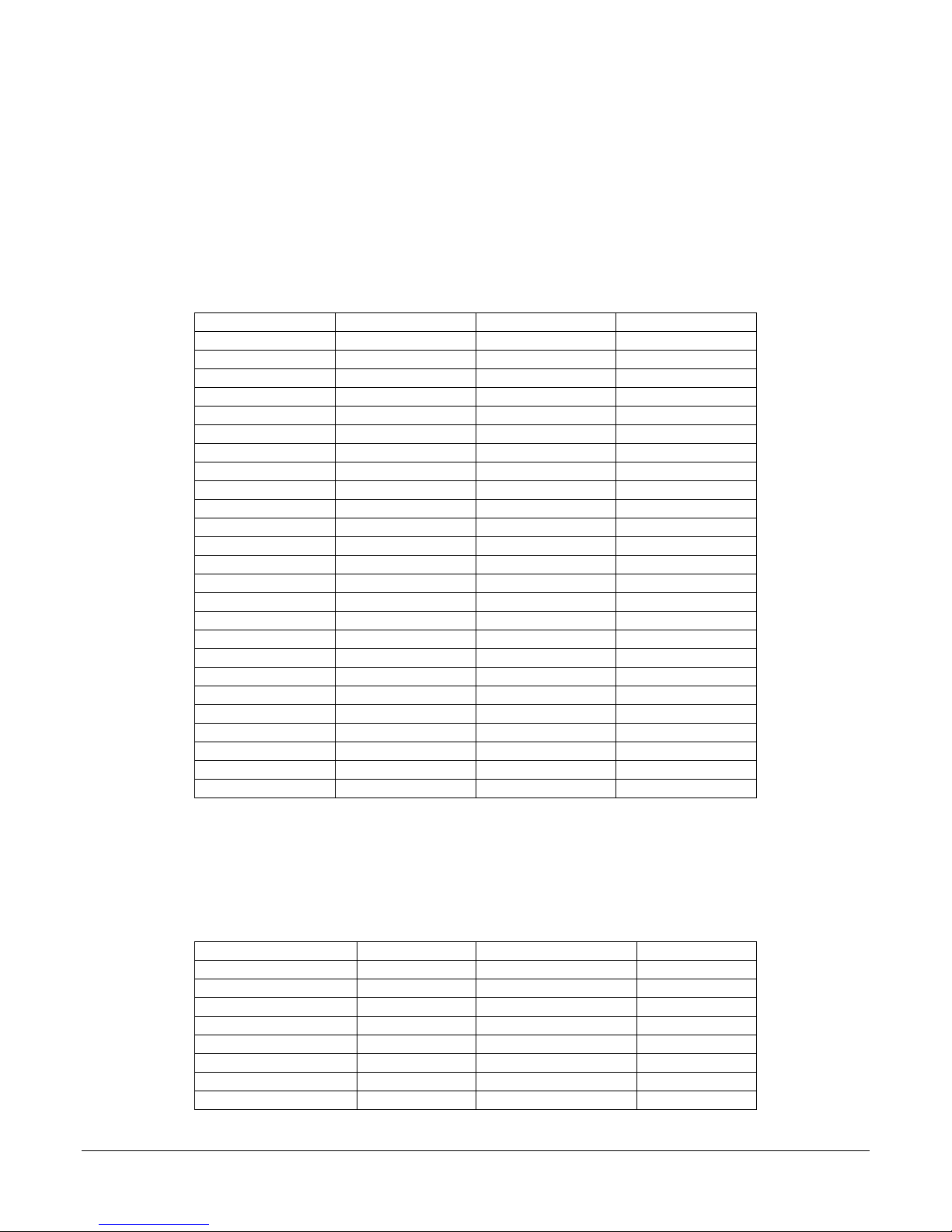
2.5 PLD Based General Purpose Digital I/O
Pin
Signal
Pin
Signal
1
PY7
2
3
PY6
4
5
PY5
6
7
PY4
8
9
PY3
10
11
PY2
12
13
PY1
14
15
PY0
16
17
PX7
18
19
PX6
20
21
PX5
22
23
PX4
24
25
PX3
26
27
PX2
28
29
PX1
30
31
PX0
32
33
PZ2
34
35
PZ1
36
37
PZ0
38
39
PE4
40
41
PE3
42
43
PE2
44
45
PE1
46
47
PE0
48
49
5V(Vcc)
50
ocessor Port Line
Description
Processor Port Line
Description
PB0
DBUS 0
PJ0
PB1
DBUS 1
PJ1
PB2
DBUS 2
PJ7
PB3
DBUS 3
PB4
DBUS 4
PB5
DBUS 5
PB6
DBUS 6
PB7
DBUS 7
These input and output lines provide connections for heavier industrial relays and switches. They are connected to the PLD
of the iPac HCS12 with the exception of lines PE0 – PE4 which are connected directly to the processor. These 5 lines with
the addition of PZ0 – PZ2 make up a dedicated input port whose input lines should not exceed 5 Vdc. The dedicated output
port lines PY0 – PY7 can drive 25 ma. loads. The open collector high drive output port PX0 – PX7 has drive 500 ma. sink
drive capability and a maximum total I/O drive of 1500 ma. for these 8 lines.
Table 3: PLD BASED DIGITAL I/O Connector (HDR1)
The PLD is connected to the HCS12 processor using pseudo data bus comprised of the processor’s port lines. Table 4 defines
these port line assignments. To access PLD Port X, perform a write with A0 = 0. To access PLD Port Y, perform a write with
A0 = 1. To access PLD Port Z, perform a read with A0 = 0.
GND
GND
GND
GND
GND
GND
GND
GND
GND
GND
GND
GND
GND
GND
GND
GND
GND
GND
GND
GND
GND
GND
GND
GND
GND
Table 4: PLD PSUEDO DATA BUS PORT LINE ASSIGNMENTS
Pr
DBUS A0
R/*W
PLD *CS
This document is the ownership of EMAC, Inc. Copyright 2003. Unauthorized duplication or copying of this document is strictly forbidden.
iPac HCS12 Manual.doc - 6 - Rev 1.2 - 11/11/03
Page 8
2.6 Analog Channels
Pin
Signal
Pin
Signal
1
ANI00
3
ANI02
4
5
ANI04
6
7
ANI06
8
9
ANI08
10
11
ANI10
12
13
ANI12
14
15
ANI14
16
17
GND
18
19
DAC00
20
21
GND
22
23
DAC02
24
25
DAC04
26
27
GND
28
29
ANI16
30
31
ANI18
32
33
ANI20
34
35
ANI22
36
37
GND
38
39
5V(Vcc)
40
Processor Port Line
Description
Processor Port Line
Description
PS4
PK3
PS5
PK4
PS6
PK5
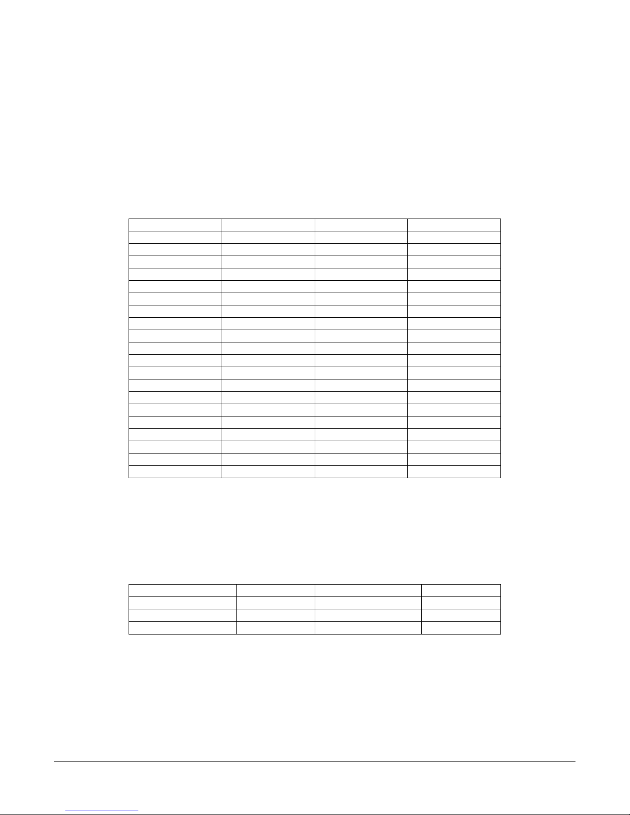
The HC12 coprocessor on the iPac HCS12 provides two independent 10 bit 8 port A/D modules. These modules provide
lines ANI00 - ANI15. In addition to the A/D, the iPac HCS12 provides 2 D/A channels that are implemented by filtering two,
8-bit hardware PWM channels PP6 & PP7. An 8 channel, 12 bit A/D and/or a 4 channel, 12 bit D/A is available optionally.
These optional analog channels are provided through external SPI devices. The A/D input channel except 0 – 5 Volt inputs.
The optional 12 bit A/D in addition to the 0 – 5 Volt inputs can be jumpered using JB1 to 5 – 20 ma. All D/A channels
provide 0 – 5 Volt outputs with a drive capability of 5 ma.
Table 5: ANALOG (HDR2)
2 ANI01
ANI03
ANI05
ANI05
ANI09
ANI11
ANI13
ANI15
GND
DAC01
GND
DAC03
DAC05
GND
ANI17
ANI19
ANI21
ANI23
GND
+VIN
In order to access the optional 12 bit A/D (LTC1290) and D/A (TLV5614) communication must take place using HCS12’s
SPI. Table 6 details these processor connection to both the 12 A/D and D/A.
Table 6: OPTIONAL A/D & D/A PORT LINE ASSIGNMENTS
This document is the ownership of EMAC, Inc. Copyright 2003. Unauthorized duplication or copying of this document is strictly forbidden.
iPac HCS12 Manual.doc - 7 - Rev 1.2 - 11/11/03
MISI
MOSI
SCLK
A/D *CS
D/A *CS
*LDAC
Page 9
Pin
Signal
DB9 Description
1
NC
-
2
NC
3
TxD
4
CTS (PH0)
-
5
RxD
6
RTS (PK0)
-
7
NC
8
NC
9
GND
-
10
NC
Pin
Signal
DB9 Description
1
-
2
NC
RS232 TXD or 422/485 TX+
3
RS232 TXD or 422/485 TX+
4
CTS (PH1)
-
5
RS232 RXD or 422/485 RX+
6
RTS (PK1)
7
8
NC
9
GND
-
10
NC
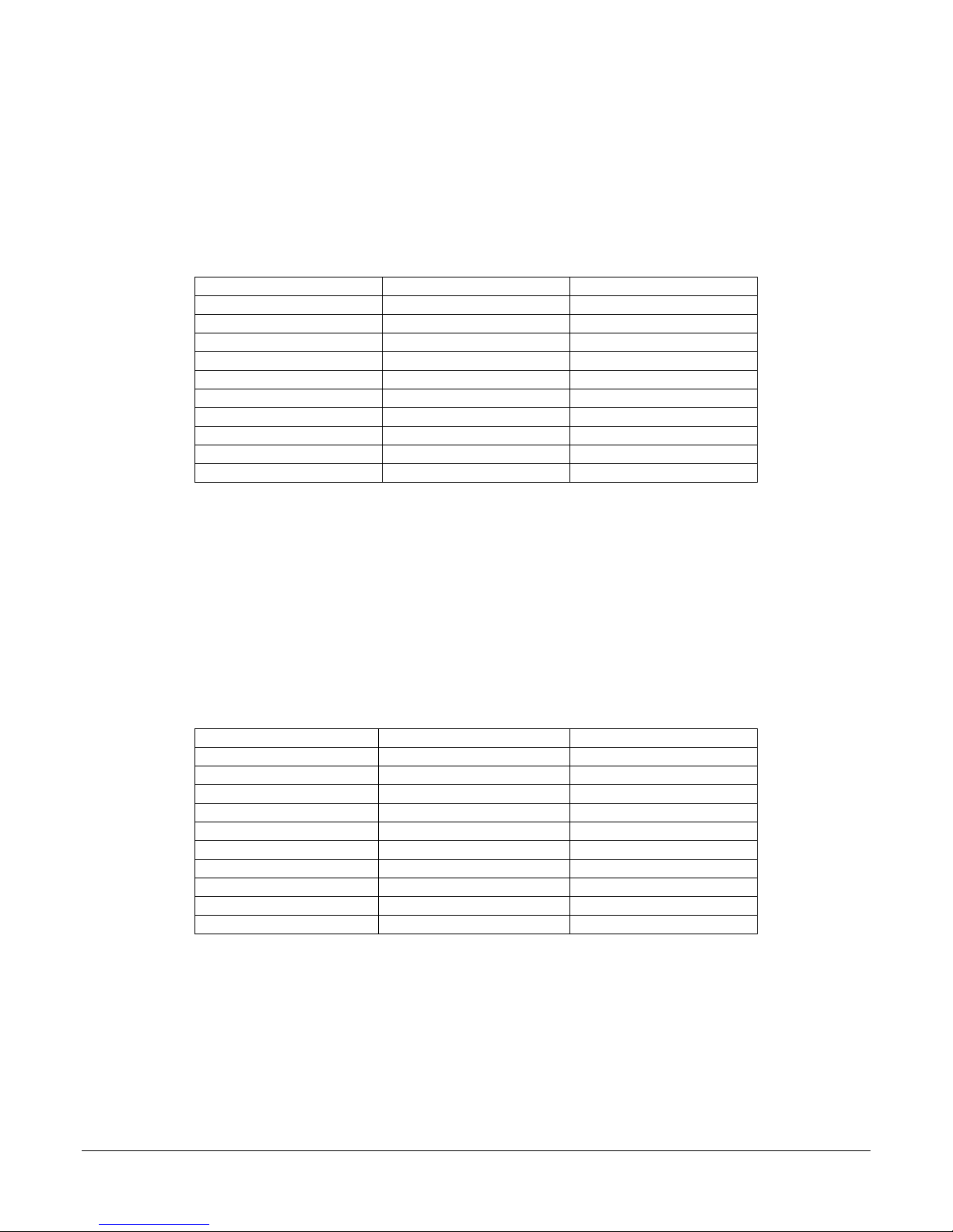
2.7 RS232 SERIAL 0 UART
The iPac HCS12 provides one dedicated RS232 UART Serial 0 which has software configurable baud rates. Both
transmission and asynchronous data reception are possible. Handshake Lines are implemented by the use of port lines PH0
and PK0.
Table 7: RS232 (HDR8)
TxD
RxD
GND
CTS (PH0)
RTS (PK0)
2.8 RS 232/422/485 SERIAL 1 UART
The iPac HCS12 provides one jumper (JP 3) selectable RS 232/422/485 UART which has software configurable baud rates.
Both transmission and asynchronous data reception are possible. RS232 Handshake Lines are implemented by the use of PH1
and PK1. When using this serial port in the RS422/485 mode, Handshake Line PK1 controls the transmitter enable line of the
RS422/485 driver.
Table 8: RS485 (HDR9)
RS422/485 TX-
RS232 RXD or 422/485 RX+
RS422/485 TX
RS422/485 RX
RS422/485 RX-
GND
CTS (PH1)
RTS (PK1)
This document is the ownership of EMAC, Inc. Copyright 2003. Unauthorized duplication or copying of this document is strictly forbidden.
iPac HCS12 Manual.doc - 8 - Rev 1.2 - 11/11/03
Page 10
2.9 CAN I/O
Pin
Signal
DB9 Description
1
NC -
2
NC
CANL
3
CANL
4
CANH -
5
GND -
6
NC -
7
NC
8
NC -
9
NC -
10
NC
Pin
Signal
DB9 Description
1
NC
-
2
NC
CANL
3
CANL
4
CANH
-
5
GND
-
6
NC
-
7
NC
8
NC
-
9
NC
-
10
NC
Pin
Signal
Pin
Signal
1
VCC
2
3
RS
4
CNTR
5 E 6
R/W*
7
D1
8
9
D3
10
11
D5
12
13
D7
14
15
K (JP1 Pin3)
16
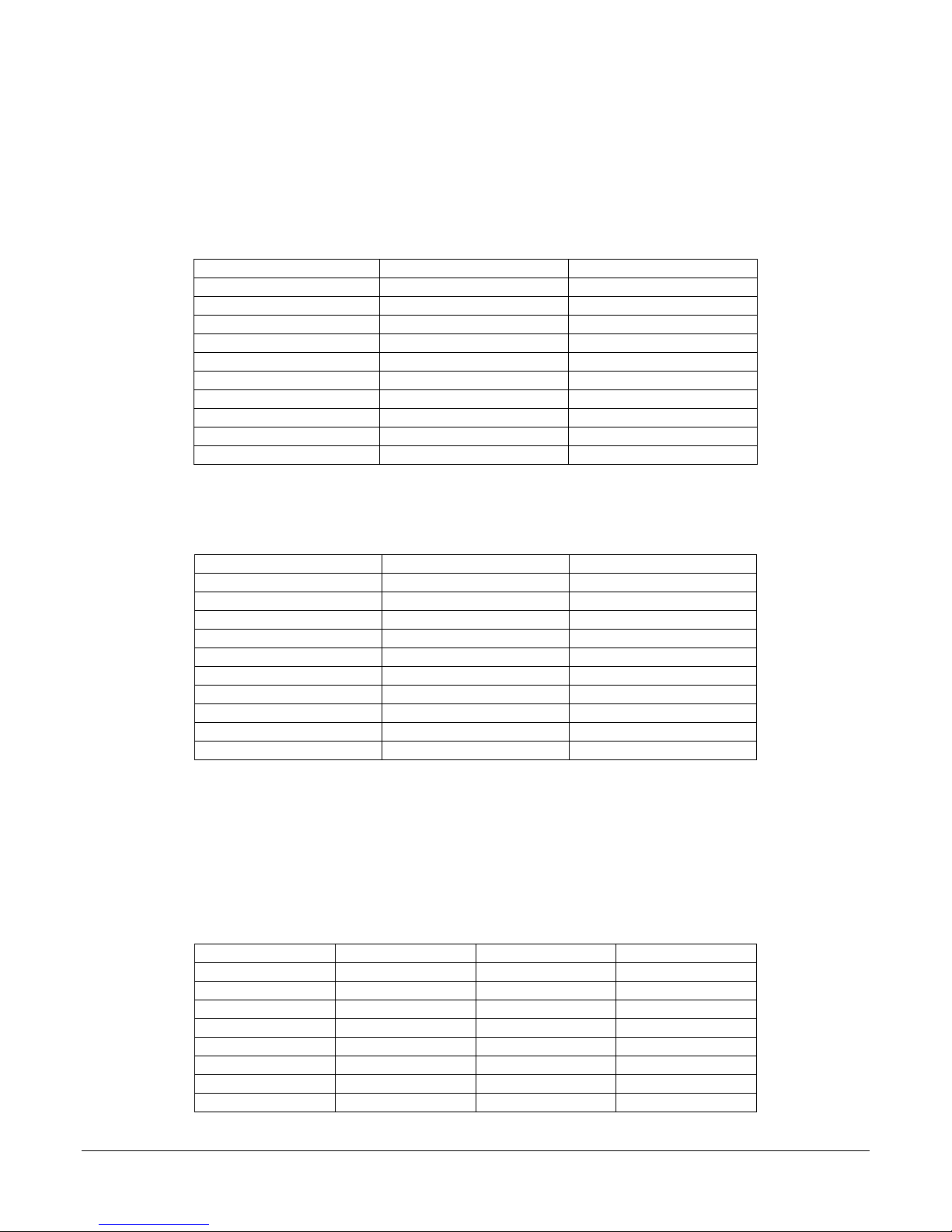
The iPac HCS12 provides a single optically coupled CAN bus with 2 connectors (in & out). The CAN bus is provided by the
processor CAN port which is available on port lines PM0 & PM1. Jumpering JP 2 enables the terminating resistor for end of
network termination.
Table 9: CAN (HDR4)
GND
CANH
Table 10: CAN (HDR5)
2.10 LCD
This header currently supports 2 and 4 line, character LCDs.
Table 11: LCD Interface (HDR6)
GND
CANH
GND
D0
D2
D4
D6
A (JP1 Pin4)
This document is the ownership of EMAC, Inc. Copyright 2003. Unauthorized duplication or copying of this document is strictly forbidden.
iPac HCS12 Manual.doc - 9 - Rev 1.2 - 11/11/03
Page 11
The LCD is connected to the HCS12 processor using pseudo data bus comprised of the processor’s port lines. Table 12
Processor Port Line
Description
Processor Port Line
Description
PB0
DBUS 0
PJ0
PB1
DBUS 1
PJ1
PB2
DBUS 2
PJ6
PB3
DBUS 3
PB4
4
LCD Backlight
PB5
DBUS 5
PB6
DBUS 6
PB7
DBUS 7
Pin
Signal
Processor Port Line
1
2
3
4
5
6
7
8
9
10
11
Processor Port Line
Description
Processor Port Line
Description
PS4
PK2
PS5
PS6
defines these port line assignments. To access PLD Port X, perform a write with A0 = 0. If using an LCD with backlight
capability set PK7 high to turn on the backlight.
Table 12: PLD PSUEDO DATA BUS PORT LINE ASSIGNMENTS
2.11 Keypad
This header provides an interface for a 4x4,4x5, or 4x6 matrix Keypad. These row and column scan lines are directly
connected to the processor.
DBUS A0
R/*W
LCD CS (E)
DBUS
PK7
Table 13: KEYPAD (HDR7)
COL6 PM7
ESD SHIELD ESD SHIELD
COL5 PM6
COL4 PM5
COL3 PM4
COL2 PM3
COL1 PM2
ROW1 PH4
ROW2 PH5
ROW 3 PH6
ROW 4 PH7
2.12 Real Time Clock (RTC)
The iPac HCS12 can be purchased with an optional battery backed real time clock (DS1305E). This clock is accessed using
the processors SPI port. This SPI port is shared with the optional 12-bit A/D & D/A. The processor port line assignments are
defined in Table 14.
Table 14: OPTIONAL RTC PORT LINE ASSIGNMENTS
This document is the ownership of EMAC, Inc. Copyright 2003. Unauthorized duplication or copying of this document is strictly forbidden.
iPac HCS12 Manual.doc - 10 - Rev 1.2 - 11/11/03
MISI
MOSI
SCLK
RTC CS
Page 12

3. Software
3.1 Introduction
The iPac HCS12 can be programmed in a variety of languages. There are a number of Free compilers, interpreters, and
assemblers available allowing the iPac to be programmed in C, Basic or Assembly languages. EMAC has written all the
drivers for the iPac board in C using Cosmic commercial C compiler/debugger and have ported these drivers to the GNU
Open Source C compiler. The Cosmic compiler can be purchased from EMAC if the customer is interested in using this
compiler and the GNU compiler can be downloaded freely from http://www.gnu-m68hc11.org/.
The resident flash on the iPac can be programmed via it's serial bootloader firmware over the RS232 com port or via it's
BDM port. Software can be written with Cosmics HC12 paged compiler or the Free GNU compiler located at
http://www.gnu-m68hc11.org/. See the associated Read-Me files for further information on the use of these compilers with
the iPac.
EMAC provides Driver object files and Demo application source code usable by the free GNU or Cosmic compilers,
allowing the user to quickly develop custom applications. Programs developed in this manner can download over the
provided serial bootloader at no extra cost to the user other than the original purchase of the hardware.
Also optionally available is a full function Modbus client software module, that turns the iPac into a fully compliant Modbus
slave. See the iPac Modbus manual for additional details.
3.2 Bootloader
The iPac serial bootloader provides a free, industry standard method for users to program the flash of an IPAC HCS12 as
opposed to the BDM cable with required software which would be purchased.
All iPacs ship with serial bootloader firmware installed within their f000 protected sector. This bootloader is activated by
shorting together pins 10 and 11 of the keypad header and then resetting the board. Once Shorted, the bootloader then issues
a menu through the RS232 port at 115200 baud. From this menu users can change the baud rate, erase the EEPROM, erase
the FLASH, and program the FLASH using the S record format.
This bootloader is a slightly modified version of Motorola’s serial bootloader. Users wanting more information should
reference the Motorola serial bootloader app note AN2153. For all programming purposes the iPac bootloader is exactly the
same except the baud rate defaults to 115200 instead of 9600.
Further documentation and an example Linux program to automatically communicate and download code to the bootloader
are provided within the GNU iPac project, located on the provided CD and available for download on the EMAC website.
This document is the ownership of EMAC, Inc. Copyright 2003. Unauthorized duplication or copying of this document is strictly forbidden.
iPac HCS12 Manual.doc - 11 - Rev 1.2 - 11/11/03
Page 13
4. PCD-39E00 Terminal Board
4.1 Introduction
The PCD-39E00 is a Terminal Board that can be used with the iPac HCS12 as well as other products. This Terminal Board is
designed to be used stacked on top of the iPac using the supplied standoffs but can be alternatively used off to the side if the
user provides longer cables.
The PCD-39E00 comes with three cables of which only two can be used at one time. The HRD2 (Analog) connector is
always used if Analog connectivity is required whereas HDR1 and HDR3 are selectively used depending on the desired
connectivity. If HDR3 has the desired connectivity then use the short 50 pin ribbon cable. If HDR1 connectivity is desired
then the long twisted cable should be used. Note the twist needs to be intact.
If connectivity to both HDR3 and HDR1 are necessary then two PCD-39E00s will be required, one which uses the short 50
pin cable and the other that uses the longer 50 pin cable with the twist.
4.2 iPac Terminal Board Pinout
The PCD-39E00 can be used with several different board thereby changing the connector descriptions for each board. There
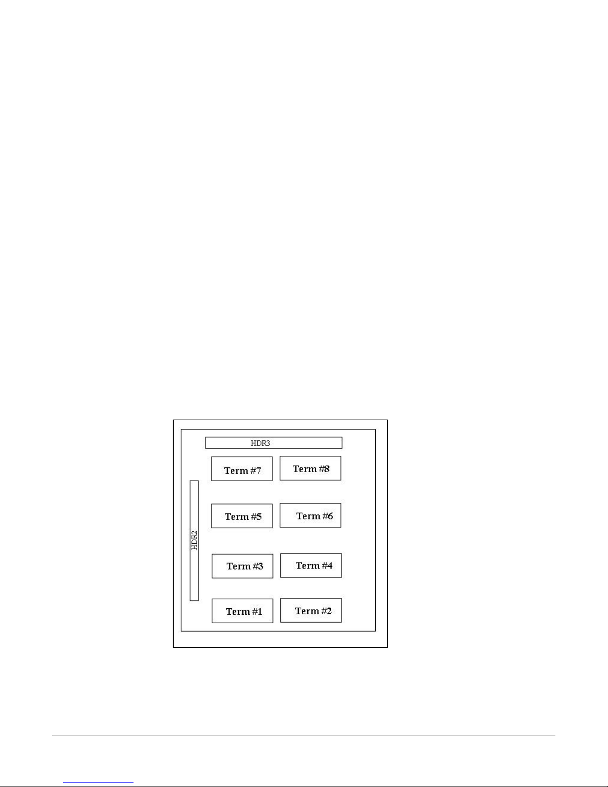
fore the specific iPac descriptions are given within the context of the iPac HCS12 manual. There are eight individual 10 pin
screw terminal connectors used on the PCD-39E00. Each is labeled STx where x is numbered from 1 to 8. The diagram
below shows the connector layout.
This document is the ownership of EMAC, Inc. Copyright 2003. Unauthorized duplication or copying of this document is strictly forbidden.
iPac HCS12 Manual.doc - 12 - Rev 1.2 - 11/11/03
Page 14

The connection of the PCD-39E00 when connected to an iPac HCS12 HDR2 and HDR3 are as follows:
Screw Terminal IPAC HDR3 Description Screw Terminal IPAC HDR2 Description
Term 5, Pin 1 Gnd Gnd Term 1, Pin 1 HDR2, Pin 39 5V
Term 5, Pin 2 HDR3, Pin 1 Port 2.7 (PH3) Term 1, Pin 2 HDR2, Pin 1 A/D0
Term 5, Pin 3 HDR3, Pin 3 Port 2.6 (PH2) Term 1, Pin 3 HDR2, Pin 2 A/D1
Term 5, Pin 4 Gnd Gnd Term 1, Pin 4 HDR2, Pin 3 A/D2
Term 5, Pin 5 HDR3, Pin 5 Port 2.5 (PP5) Term 1, Pin 5 HDR2, Pin 4 A/D3
Term 5, Pin 6 HDR3, Pin 7 Port 2.4 (PP4) Term 1, Pin 6 HDR2, Pin 5 A/D4
Term 5, Pin 7 Gnd Gnd Term 1, Pin 7 HDR2, Pin 6 A/D5
Term 5, Pin 8 HDR3, Pin 9 Port 2.3 (PP3) Term 1, Pin 8 HDR2, Pin 7 A/D6
Term 5, Pin 9 HDR3, Pin 11 Port 2.2 (PP2) Term 1, Pin 9 HDR2, Pin 8 A/D7
Term 5, Pin 10 Gnd Gnd Term 1, Pin 10 Gnd Gnd
Term 6, Pin 1 HDR3, Pin 13 Port 2.1 (PP1) Term 2, Pin 11 HDR2, Pin 39 5V
Term 6, Pin 2 HDR3, Pin 15 Port 2.0 (PP0) Term 2, Pin 12 HDR2, Pin 9 A/D8
Term 6, Pin 3 Gnd Gnd Term 2, Pin 13 HDR2, Pin 10 A/D9
Term 6, Pin 4 HDR3, Pin 17 Port 1.7 (PT7) Term 2, Pin 14 HDR2, Pin 11 A/D10
Term 6, Pin 5 HDR3, Pin 19 Port 1.6 (PT6) Term 2, Pin 15 HDR2, Pin 12 A/D11
Term 6, Pin 6 Gnd Gnd Term 2, Pin 16 HDR2, Pin 13 A/D12
Term 6, Pin 7 HDR3, Pin 21 Port 1.5 (PT5) Term 2, Pin 17 HDR2, Pin 14 A/D13
Term 6, Pin 8 HDR3, Pin 23 Port 1.4 (PT4) Term 2, Pin 18 HDR2, Pin 15 A/D14
Term 6, Pin 9 Gnd Gnd Term 2, Pin 19 HDR2, Pin 16 A/D15
Term 6, Pin 10 HDR3, Pin 49 (5V) 5V Term 2, Pin 20 Gnd Gnd
Term 7, Pin 1 Gnd Gnd Term 3, Pin 1 HDR2, Pin 39 5V
Term 7, Pin 2 HDR3, Pin 25 Port 1.3 (PT3) Term 3, Pin 2 HDR2, Pin 40 +Vin
Term 7, Pin 3 HDR3, Pin 27 Port 1.2 (PT2) Term 3, Pin 3 HDR2, Pin 19 D/A0
Term 7, Pin 4 Gnd Gnd Term 3, Pin 4 HDR2, Pin 20 D/A1
Term 7, Pin 5 HDR3, Pin 29 Port 1.1 (PT1) Term 3, Pin 5 Gnd Gnd
Term 7, Pin 6 HDR3, Pin 31 Port 1.0 (PT0) Term 3, Pin 6 HDR2, Pin 23 D/A2
Term 7, Pin 7 Gnd Gnd Term 3, Pin 7 HDR2, Pin 24 D/A3
Term 7, Pin 8 HDR3, Pin 33 Port 0.7 (PA7) Term 3, Pin 8 HDR2, Pin 25 D/A4
Term 7, Pin 9 HDR3, Pin 35 Port 0.6 (PA6) Term 3, Pin 9 HDR2, Pin 26 D/A5
Term 7, Pin 10 Gnd Gnd Term 3, Pin 10 Gnd Gnd
Term 8, Pin 1 HDR3, Pin 37 Port 0.5 (PA5) Term 4, Pin 11 HDR2, Pin 39 5V
Term 8, Pin 2 HDR3, Pin 39 Port 0.4 (PA4) Term 4, Pin 12 HDR2, Pin 29 A/D16
Term 8, Pin 3 Gnd Gnd Term 4, Pin 13 HDR2, Pin 30 A/D17
Term 8, Pin 4 HDR3, Pin 41 Port 0.3 (PA3) Term 4, Pin 14 HDR2, Pin 31 A/D18
Term 8, Pin 5 HDR3, Pin 43 Port 0.2 (PA2) Term 4, Pin 15 HDR2, Pin 32 A/D19
Term 8, Pin 6 Gnd Gnd Term 4, Pin 16 HDR2, Pin 33 A/D20
Term 8, Pin 7 HDR3, Pin 45 Port 0.1 (PA1) Term 4, Pin 17 HDR2, Pin 34 A/D21
Term 8, Pin 8 HDR3, Pin 47 Port 0.0 (PA0) Term 4, Pin 18 HDR2, Pin 35 A/D22
Term 8, Pin 9 Gnd Gnd Term 4, Pin 19 HDR2, Pin 36 A/D23
Term 8, Pin 10 HDR3, Pin 49 (5V) 5V Term 4, Pin 20 Gnd Gnd
This document is the ownership of EMAC, Inc. Copyright 2003. Unauthorized duplication or copying of this document is strictly forbidden.
iPac HCS12 Manual.doc - 13 - Rev 1.2 - 11/11/03
Page 15

The connection of the PCD-39E00 when connected to an iPac HCS12 HDR1 and HDR2 are as follows:
Screw Terminal IPAC HDR1 Description Screw Terminal IPAC HDR2 Description
Term 5, Pin 1 Gnd Gnd Term 1, Pin 1 HDR2, Pin 39 5V
Term 5, Pin 2 HDR1, Pin 1 Port 2.7 (Y7) Term 1, Pin 2 HDR2, Pin 1 A/D0
Term 5, Pin 3 HDR1, Pin 3 Port 2.6 (Y6) Term 1, Pin 3 HDR2, Pin 2 A/D1
Term 5, Pin 4 Gnd Gnd Term 1, Pin 4 HDR2, Pin 3 A/D2
Term 5, Pin 5 HDR1, Pin 5 Port 2.5 (Y5) Term 1, Pin 5 HDR2, Pin 4 A/D3
Term 5, Pin 6 HDR1, Pin 7 Port 2.4 (Y4) Term 1, Pin 6 HDR2, Pin 5 A/D4
Term 5, Pin 7 Gnd Gnd Term 1, Pin 7 HDR2, Pin 6 A/D5
Term 5, Pin 8 HDR1, Pin 9 Port 2.3 (Y3) Term 1, Pin 8 HDR2, Pin 7 A/D6
Term 5, Pin 9 HDR1, Pin 11 Port 2.2 (Y2) Term 1, Pin 9 HDR2, Pin 8 A/D7
Term 5, Pin 10 Gnd Gnd Term 1, Pin 10 Gnd Gnd
Term 6, Pin 1 HDR1, Pin 11 Port 2.1 (Y1) Term 2, Pin 11 HDR2, Pin 39 5V
Term 6, Pin 2 HDR1, Pin 15 Port 2.0 (Y0) Term 2, Pin 12 HDR2, Pin 9 A/D8
Term 6, Pin 3 Gnd Gnd Term 2, Pin 13 HDR2, Pin 10 A/D9
Term 6, Pin 4 HDR1, Pin 17 Port 1.7 (X7) Term 2, Pin 14 HDR2, Pin 11 A/D10
Term 6, Pin 5 HDR1, Pin 19 Port 1.6 (X6) Term 2, Pin 15 HDR2, Pin 12 A/D11
Term 6, Pin 6 Gnd Gnd Term 2, Pin 16 HDR2, Pin 13 A/D12
Term 6, Pin 7 HDR1, Pin 21 Port 1.5 (X5) Term 2, Pin 17 HDR2, Pin 14 A/D13
Term 6, Pin 8 HDR1, Pin 23 Port 1.4 (X4) Term 2, Pin 18 HDR2, Pin 15 A/D14
Term 6, Pin 9 Gnd Gnd Term 2, Pin 19 HDR2, Pin 16 A/D15
Term 6, Pin 10 HDR1, Pin 49 (5V) 5V Term 2, Pin 20 Gnd Gnd
Term 7, Pin 1 Gnd Gnd Term 3, Pin 1 HDR2, Pin 39 5V
Term 7, Pin 2 HDR1, Pin 25 Port 1.3 (X3) Term 3, Pin 2 HDR2, Pin 40 +Vin
Term 7, Pin 3 HDR1, Pin 27 Port 1.2 (X2) Term 3, Pin 3 HDR2, Pin 19 D/A0
Term 7, Pin 4 Gnd Gnd Term 3, Pin 4 HDR2, Pin 20 D/A1
Term 7, Pin 5 HDR1, Pin 29 Port 1.1 (X1) Term 3, Pin 5 Gnd Gnd
Term 7, Pin 6 HDR1, Pin 31 Port 1.0 (X0) Term 3, Pin 6 HDR2, Pin 23 D/A2
Term 7, Pin 7 Gnd Gnd Term 3, Pin 7 HDR2, Pin 24 D/A3
Term 7, Pin 8 HDR1, Pin 33 Port 0.7 (Z2) Term 3, Pin 8 HDR2, Pin 25 D/A4
Term 7, Pin 9 HDR1, Pin 35 Port 0.6 (Z1) Term 3, Pin 9 HDR2, Pin 26 D/A5
Term 7, Pin 10 Gnd Gnd Term 3, Pin 10 Gnd Gnd
Term 8, Pin 1 HDR1, Pin 37 Port 0.5 (Z0) Term 4, Pin 11 HDR2, Pin 39 5V
Term 8, Pin 2 HDR1, Pin 39 Port 0.4 (E4) Term 4, Pin 12 HDR2, Pin 29 A/D16
Term 8, Pin 3 Gnd Gnd Term 4, Pin 13 HDR2, Pin 30 A/D17
Term 8, Pin 4 HDR1, Pin 41 Port 0.3 (E3) Term 4, Pin 14 HDR2, Pin 31 A/D18
Term 8, Pin 5 HDR1, Pin 43 Port 0.2 (E2) Term 4, Pin 15 HDR2, Pin 32 A/D19
Term 8, Pin 6 Gnd Gnd Term 4, Pin 16 HDR2, Pin 33 A/D20
Term 8, Pin 7 HDR1, Pin 45 Port 0.1 (E1) Term 4, Pin 17 HDR2, Pin 34 A/D21
Term 8, Pin 8 HDR1, Pin 47 Port 0.0 (E0) Term 4, Pin 18 HDR2, Pin 35 A/D22
Term 8, Pin 9 Gnd Gnd Term 4, Pin 19 HDR2, Pin 36 A/D23
Term 8, Pin 10 HDR1, Pin 49 (5V) 5V Term 4, Pin 20 Gnd Gnd
This document is the ownership of EMAC, Inc. Copyright 2003. Unauthorized duplication or copying of this document is strictly forbidden.
iPac HCS12 Manual.doc - 14 - Rev 1.2 - 11/11/03
 Loading...