

ELPIDA PD488588FF-C80-40-DH1 Datasheet

DATA SHEET
288M bits Direct Rambus DRAM
for High Performance Solution
µµµµ
PD488588FF-C80-40 (512K words ×××× 18 bits ×××× 32s banks)
Description
The Direct Rambus DRAM (Direct RDRAM) is a
general purpose high-performance memory device
suitable for use in a broad range of applications
including computer memory, graphics, video, and any
other application where high bandwidth and low
latency are required.
PD488588FF is 288Mbits Direct Rambus DRAM
µ
The
(RDRAM
The use of Rambus Signaling Level (RSL) technology
permits 800MHz transfer rates while using
conventional system and board design technologies.
Direct RDRAM devices are capable of sustained data
transfers at 1.25ns per two bytes (10ns per sixteen
bytes).
The architecture of the Direct RDRAMs allows the
highest sustained bandwidth for multiple, simultaneous
randomly addressed memory transactions.
The separate control and data buses with independent
row and column control yield over 95% bus efficiency.
The Direct RDRAM’s four banks support up to four
simultaneous transactions.
System oriented features for mobile, graphics and
large memory systems include power management,
byte masking.
The
package suitable for desktop as well as low-profile
add-in card and mobile applications. Direct RDRAMs
operate from a 2.5V
), organized as 16M words by 18 bits.
PD488588FF is offered in a CSP horizontal
µ
supply.
Features
• Highest sustained bandwidth per DRAM device
— 1.6 GB/s sustained data transfer rate
— Separate control and data buses for maximized
efficiency
— Separate row and column control buses for easy
scheduling and highest performance
— 32 banks: four transactions can take place
simultaneously at full bandwidth data rates
• Low latency features
— Write buffer to reduce read latency
— 3 precharge mechanisms for controller flexibility
— Interleaved transactions
• Advanced power management:
— Multiple low power states allows flexibility in power
consumption versus time to active state
— Power-down self-refresh
• Overdrive current mode
• Organization: 2K bytes pages and 32 banks, x 18
• Uses Rambus Signaling Level (RSL) for up to
800MHz operation
• Package : 80-ball FBGA (
BGA) (17.16 × 10.2)
µ
Application
The µPD488588FF is most appropriate for the
applications, such as consumer products demanding
vivid animations, processor memory for multimedia
and 3D graphics, network processing and storage
systems requiring scalability to accommodate future
designs.
Document No. E0251N20 (Ver. 2.0)
Date Published July 2002 (K) Japan
URL: http://www.elpida.com
Elpida Memory,Inc. 2002
Elpida Memory, Inc. is a joint venture DRAM company of NEC Corporation and Hitachi, Ltd.

µµµµ
PD488588FF-C80-40
Ordering Information
Part number
PD488588FF-C80-40-DH1 512K x 18 x 32s 800 40
µ
Note: The “32s” designation indicates that this RDRAM core is composed of 32 banks which use a “split” bank
architecture
Organization*
words × bits × Internal
Banks
Clock frequency
MHz (max.)
/RAS access
time (ns)
Package
80-ball FBGA (
(17.16 × 10.2)
BGA)
µ
2
Data Sheet E0251N20 (Ver. 2.0)
µµµµ
PD488588FF-C80-40
Pin Configuration
80-ball FBGA (
µµµµ
BGA) (17.16 ×
× 10.2)
××
Top View
10 O O O O
9
8 O O O O O O O O O O O O O O O O O O
7 O O O O O O O O O O O O O O O O O O
6
5
4 O O O O O O O O O O O O O O O O O O
3 O O O O O O O O O O O O O O O O O O
2
1 O O O O
A B C D E F G H J K L M N P R S T U
VDD
10
9
GND
8
VDD
7
6
5
GND GND DQA6 DQA4 DQA2 DQA0 CFM CFMN ROW1 COL4 COL2 COL0 DQB0 DQB2 DQB4 DQB6 GND GND
4
VDD
3
2
1
GND
VDD
CMD
DQA8 DQA7 DQA5 DQA3 DQA1 CTMN CTM ROW2 ROW0 COL3 COL1 DQB1 DQB3 DQB5 DQB7 DQB8
GND SCK VCMOS GND
VDD
GND GND
VDD
GND GNDa GNDa
VDD
GND
VDD VDD
VDDa
REF
V
GND GND
VDD
GND
VDD VDD
GND GND
GND GND VCMOS
VDD
GND
SIO0 SIO1 GND
VDD
VDD
VDD
A B C D E F G H J K L M N P R S T U
Note Some signals can be applied because this pin is not connected to the inside of the chip.
GND
VDD
VDD
Data Sheet E0251N20 (Ver. 2.0)
3
µµµµ
PD488588FF-C80-40
Pin Description
Signal Input / Output Type #pins Description
Note1
Note2
Note2
Note2
Note2
Note2
Note2
Note2
Note2
2 Serial input/output. Pi ns for reading from and writing to the c ont rol regi sters using
a serial access protocol. Also used for power management .
Note1
1 Command input. Pins used in conjunction with SIO0 and SIO1 for reading from
and writing to the control regis ters. Also used for power management.
Note1
1 Serial clock input. Cl ock source used for reading from and writing to the control
registers.
9 Data byte A. Nine pins whic h carry a byte of read or write data between the
Channel and the RDRAM.
1 Clock from master. Interface clock used for receiving RSL signals from the
Channel. Positive polarity.
1 Clock from master. Interface clock used for receiving RSL signals from the
Channel. Negative polarity.
1 Clock to master. I nt e rf ace clock used for trans m i tting RSL signals to the Channel .
Negative polarity.
1 Clock to master. I nt e rf ace clock used for trans m i tting RSL signals to the Channel .
Positive polarity.
3 Row access control. Three pi ns containing control and address i nformation for
row accesses.
5 Column access control. Five pins containing cont rol and address information for
column accesses.
9 Data byte B. Nine pins whic h carry a byte of read or write data between the
Channel and the RDRAM.
SIO0, SIO1 Input / Output
CMD Input
SCK Input
CMOS
CMOS
CMOS
VDD 18 Supply voltage f or the RDRAM core and interface logic .
V
1 Supply voltage for the RDRAM anal og circuitry.
DDa
V
2 Supply voltage for CMOS input /output pins.
CMOS
GND 22 Ground reference for RDRAM core and i nterface.
GNDa 2 Ground reference for RDRAM analog circui try.
DQA8..DQA0 Input / Output
CFM Input
CFMN Input
V
1 Logic threshold reference voltage f or RS L signals.
REF
CTMN Input
CTM Input
ROW2..ROW0 Input
COL4..COL0 Input
DQB8..DQB0 Input / Output
RSL
RSL
RSL
RSL
RSL
RSL
RSL
RSL
Total pin count per package 80
Notes 1. All CMOS signals are high-true ; a high voltage is a logic one and a low voltage is logic zero.
2. All RSL signals are low-true ; a low voltage is a logic one and a high voltage is logic zero.
4
Data Sheet E0251N20 (Ver. 2.0)
µµµµ
PD488588FF-C80-40
Block Diagram
RQ7..RQ5 or
ROW2..ROW0
9 9
3
CTMDQB8..DQB0 DQA8..DQA0CTMN
RCLK
SCK, CMD2SIO0, SIO1
2
CFM CFMN
1:8 Demux
RQ4..RQ0 or
COL4..COL0
5
1:8 Demux
RCLK
Packet Decode
ROWR ROWA
11 5 5 9
ROPAVDR BR R CMBMACOPSDC BCXOPMDX BX
Internal DQB Data Path
9
RCLK
9
1:8 Demux
DM
Row Decode
9
Write Buffer
Mux
Sense Amp
64x72
72
72
PRER
ACT
DRAM Core
64x72
0
SAmp
0/1
SAmp
1/2
SAmp
•
•
•
13/14
SAmp
14/15
SAmp
15
SAmp
TCLK
512x128x144
Control Registers
Power Modes
Bank 0
Bank 1
Bank 2
•
•
•
Bank 13
Bank 14
Bank 15
RCLK
Packet Decode
6
5
5
DEVIDREFR
XOP Decode
PREX
64x72
0
0/1
1/2
13/14
SAmp
SAmp
SAmp
•
•
•
SAmp
5
72
5
MatchMatch Match
72
5
Write
Buffer
Mux Mux
Column Decode & Mask
PREC RD, WR
Internal DQA Data Path
9
Write Buffer
SAmp
14/15
SAmp
15
7
9
COLMCOLCCOLX
8
8
RCLK
1:8 Demux
9
SAmp
16
SAmp
16/17
SAmp
TCLK
17/18
SAmp
•
9
•
•
8:1 Mux
29/30
SAmp
30/31
SAmp
31
SAmp
Bank 16
Bank 17
Bank 18
•
•
•
Bank 29
Bank 30
Bank 31
16
16/17
17/18
•
•
•
29/30
30/31
31
SAmp
SAmp
SAmp
SAmp
SAmp
99
TCLK
8:1 Mux
9
Data Sheet E0251N20 (Ver. 2.0)
5

µµµµ
PD488588FF-C80-40
CONTENTS
1. General Description.................................................................................................................................................8
2. Packet Format........................................................................................................................................................10
3. Field Encoding Summary......................................................................................................................................12
4. DQ Packet Timing..................................................................................................................................................14
5. COLM Packet to D Packet Mapping...................................................................................................................... 14
6. ROW-to-ROW Packet Interaction..........................................................................................................................16
7. ROW-to-COL Packet Interaction...........................................................................................................................18
8. COL-to-COL Packet Interaction............................................................................................................................19
9. COL-to-ROW Packet Interaction...........................................................................................................................20
10. ROW-to-ROW Examples......................................................................................................................................21
11. Row and Column Cycle Description ..................................................................................................................22
12. Precharge Mechanisms.......................................................................................................................................23
13. Read Transaction - Example...............................................................................................................................25
14. Write Transaction - Example...............................................................................................................................26
15. Write/Retire - Examples.......................................................................................................................................27
16. Interleaved Write - Example................................................................................................................................29
17. Interleaved Read - Example................................................................................................................................30
18. Interleaved RRWW - Example.............................................................................................................................31
19. Control Register Transactions............................................................................................................................32
20. Control Register Packets ....................................................................................................................................33
21. Initialization..........................................................................................................................................................34
22. Control Register Summary..................................................................................................................................38
23. Power State Management....................................................................................................................................47
24. Refresh..................................................................................................................................................................52
25. Current and Temperature Control......................................................................................................................54
26. Electrical Conditions ...........................................................................................................................................55
27. Timing Conditions ...............................................................................................................................................56
28. Electrical Characteristics....................................................................................................................................58
29. Timing Characteristics ........................................................................................................................................58
30. RSL Clocking........................................................................................................................................................59
31. RSL - Receive Timing ..........................................................................................................................................60
32. RSL - Transmit Timing.........................................................................................................................................61
33. CMOS - Receive Timing.......................................................................................................................................62
34. CMOS - Transmit Timing.....................................................................................................................................64
35. RSL - Domain Crossing Window........................................................................................................................65
36. Timing Parameters...............................................................................................................................................66
37. Absolute Maximum Ratings................................................................................................................................67
6
Data Sheet E0251N20 (Ver. 2.0)

µµµµ
PD488588FF-C80-40
38. IDD - Supply Current Profile .................................................................................................................................67
39. Capacitance and Inductance ..............................................................................................................................68
40. Interleaved Device Mode.....................................................................................................................................70
41. Glossary of Terms ...............................................................................................................................................74
42. Package Drawing.................................................................................................................................................76
43. Recommended Soldering Conditions................................................................................................................77
Data Sheet E0251N20 (Ver. 2.0)
7

µµµµ
PD488588FF-C80-40
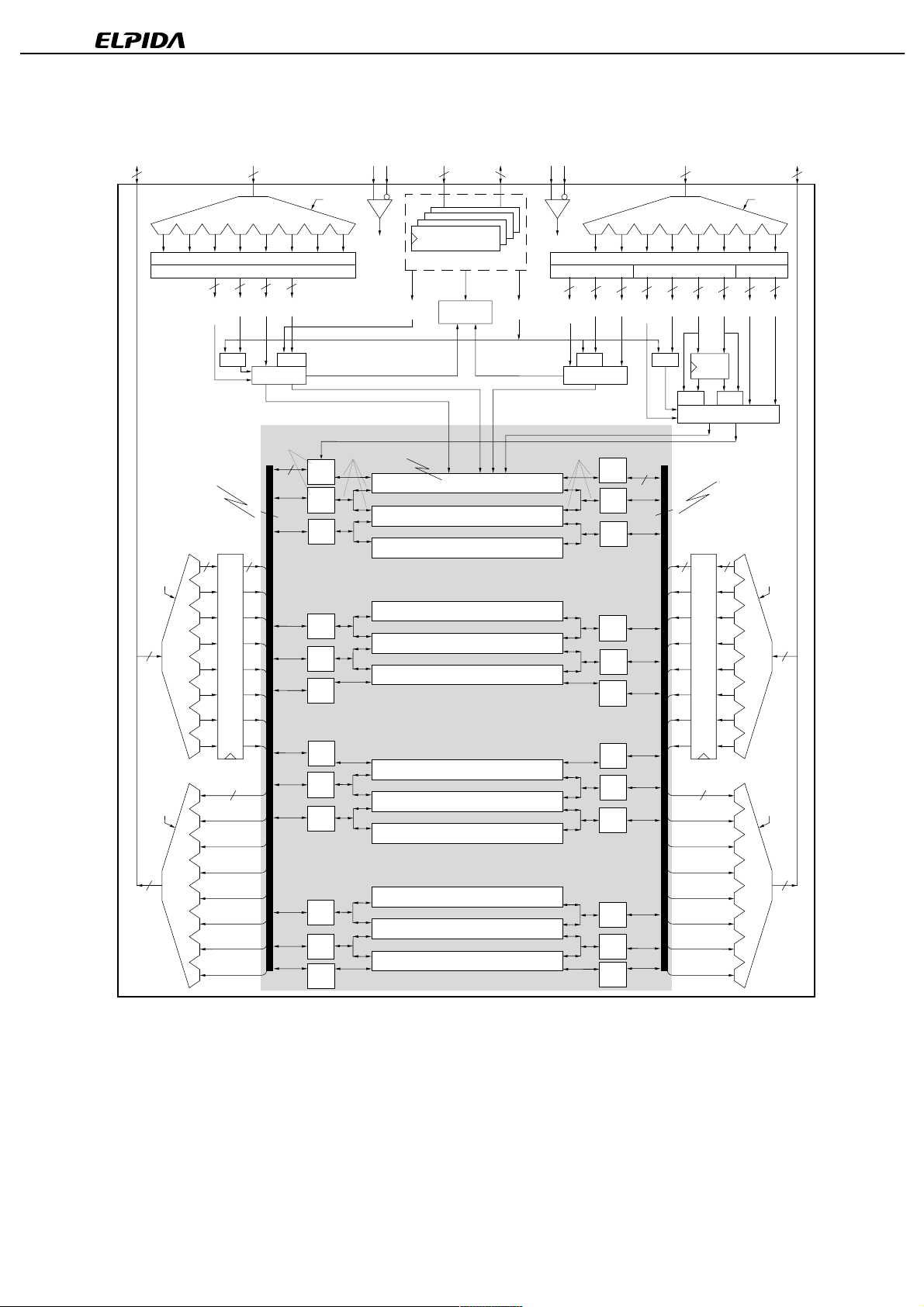
1. General Description
The figure on page 5 is a block diagram of the
banks and sense amps similar to those found in other types of DRAM, and a Direct Rambus interface block which
permits an external controller to access this core at up to 1.6 GB/s.
Control Registers: The CMD, SCK, SIO0, and SIO1 pins appear in the upper center of the block diagram. They are
used to write and read a block of control registers. These registers supply the RDRAM configuration information to a
controller and they select the operating modes of the device. The nine bit REFR value is used for tracking the last
refreshed row. Most importantly, the five bits DEVID specifies the device address of the RDRAM on the Channel.
Clocking: The CTM and CTMN pins (Clock-To-Master) generate TCLK (Transmit Clock), the internal clock used to
transmit read data. The CFM and CFMN pins (Clock-From-Master) generate RCLK (Receive Clock), the internal
clock signal used to receive write data and to receive the ROW and COL pins.
DQA, DQB Pins: These 18 pins carry read (Q) and write (D) data across the Channel. They are multiplexed / de-
multiplexed from / to two 72-bit data paths (running at one-eighth the data frequency) inside the RDRAM.
Banks: The 32 Mbyte core of the RDRAM is divided into 32 one-Mbyte banks, each organized as 512 rows, with
each row containing 128 dualocts (2K bytes), and each dualoct containing 16 bytes. A dualoct is the smallest unit of
data that can be addressed.
Sense Amps: The RDRAM contains 34 sense amps. Each sense amp consists of 1,024 bytes of fast storage (512
for DQA and 512 for DQB) and can hold one-half of one row of one bank of the RDRAM. The sense amp may hold
any of the 512 half-rows of an associated bank. However, each sense amp is shared between two adjacent banks of
the RDRAM (except for numbers 0, 15, 30, and 31). This introduces the restriction that adjacent banks may not be
simultaneously accessed.
RQ Pins: These pins carry control and address information. They are broken into two groups. RQ7..RQ5 are also
called ROW2..ROW0, and are used primarily for controlling row accesses. RQ4..RQ0 are also called COL4..COL0,
and are used primarily for controlling column accesses.
ROW Pins: The principle use of these three pins is to manage the transfer of data between the banks and the sense
amps of the RDRAM. These pins are de-multiplexed into a 24-bit ROWA (row-activate) or ROWR (row-operation)
packet.
COL Pins: The principle use of these five pins is to manage the transfer of data between the DQA/DQB pins and the
sense amps of the RDRAM. These pins are de-multiplexed into a 23-bit COLC (column-operation) packet and either
a 17-bit COLM (mask) packet or a 17-bit COLX (extended-operation) packet.
ACT Command: An ACT (activate) command from an ROWA packet causes one of the 512 rows of the selected
bank to be loaded to its associated sense amps (two 512 byte sense amps for DQA and two for DQB).
PRER Command: A PRER (precharge) command from an ROWR packet causes the selected bank to release its
two associated sense amps, permitting a different row in that bank to be activated, or permitting adjacent banks to be
activated.
PD488588. It consists of two major blocks : a “core” block built from
µ
8
Data Sheet E0251N20 (Ver. 2.0)

µµµµ
PD488588FF-C80-40
RD Command: The RD (read) command causes one of the 128 dualocts of one of the sense amps to be transmitted
on the DQA/DQB pins of the Channel.
WR Command: The WR (write) command causes a dualoct received from the DQA/DQB data pins of the Channel to
be loaded into the write buffer. There is also space in the write buffer for the BC bank address and C column
address information. The data in the write buffer is automatically retired (written with optional bytemask) to one of the
128 dualocts of one of the sense amps during a subsequent COP command. A retire can take place during a RD,
WR, or NOCOP to another device, or during a WR or NOCOP to the same device. The write buffer will not retire
during a RD to the same device. The write buffer reduces the delay needed for the internal DQA/DQB data path turnaround.
PREC Precharge: The PREC, RDA and WRA commands are similar to NOCOP, RD and WR, except that a precharge
operation is performed at the end of the column operation. These commands provide a second mechanism for
performing precharge.
PREX Precharge: After a RD command, or after a WR command with no byte masking (M=0), a COLX packet may
be used to specify an extended operation (XOP). The most important XOP command is PREX. This command
provides a third mechanism for performing precharge.
Data Sheet E0251N20 (Ver. 2.0)
9
µµµµ
PD488588FF-C80-40
2. Packet Format
Figure 2-1 shows the formats of the ROWA and ROWR packets on the ROW pins. Table 2-1 describes the fields
which comprise these packets. DR4T and DR4F bits are encoded to contain both the DR4 device address bit and a
framing bit which allows the ROWA or ROWR packet to be recognized by the RDRAM.
The AV (ROWA/ROWR packet selection) bit distinguishes between the two packet types. Both the ROWA and
ROWR packet provide a five bit device address and a four bit bank address. An ROWA packet uses the remaining
bits to specify a nine bit row address, and the ROWR packet uses the remaining bits for an eleven bit opcode field.
Note the use of the “RsvX” notation to reserve bits for future address field extension.
Figure 2-1 also shows the formats of the COLC, COLM, and COLX packets on the COL pins. Table 2-2 describes
the fields which comprise these packets.
The COLC packet uses the S (Start) bit for framing. A COLM or COLX packet is aligned with this COLC packet, and
is also framed by the S bit.
The 23 bit COLC packet has a five bit device address, a four bit bank address, a six bit column address, and a four
bit opcode. The COLC packet specifies a read or write command, as well as some power management commands.
The remaining 17 bits are interpreted as a COLM (M=1) or COLX (M=0) packet. A COLM packet is used for a
COLC write command which needs bytemask control. The COLM packet is associated with the COLC packet from a
time t
device address, a four bit bank address, and a five bit opcode. The COLX packet may also be used to specify some
housekeeping and power management commands. The COLX packet is framed within a COLC packet but is not
otherwise associated with any other packet.
earlier. An COLX packet may be used to specify an independent precharge command. It contains a five bit
RTR
Table 2-1 Field Description for ROWA Packet and ROWR Packet
Field Description
DR4T, DR4F Bits for framing (recognizing) a ROWA or ROWR packet. Also encodes highest device address bi t.
DR3..DR0 Device address for ROWA or ROWR pac ket.
BR4..BR0 Bank address for ROWA or ROWR pack et. RsvB denotes bits i gnored by the RDRAM.
AV Selects between ROWA packet (AV=1) and ROWR packet (AV=0).
R8..R0 Row address for ROWA packet. RsvR denotes bits reserved for future row address ext ension.
ROP10..ROP0 Opcode field for ROWR packet. Specifies precharge, refres h, and power m anagement functions.
Table 2-2 Field Description for COLC Packet, COLM Packet, and COLX Packet
Field Description
S Bit for framing (recognizing) a COLC packet, and indirectly for framing COLM and COLX packets.
DC4..DC0 Device address for COLC packet.
BC4..BC0 Bank address for COLC packet . RsvB denotes bits reserved for future extension (controller drivers 0's).
C6..C0 Column address for COLC packet.
COP3..COP0 Opcode field for COLC packet. S pecifies read, write, precharge, and power management functions.
M Selects between COLM pack et (M=1) and COLX packet (M=0).
MA7..MA0 Bytemask write c ontrol bits. 1=write, 0=no-write. MA0 controls the earlies t byte on DQA8..0.
MB7..MB0 Bytemask write c ontrol bits. 1=write, 0=no-write. MB0 controls the earlies t byte on DQB8..0.
DX4..DX0 Device address for COLX pac ket.
BX4..BX0 Bank address for COLX pack et. RsvB denotes bits reserved for future extension (controller drivers 0's).
XOP4..XOP0 Opcode field for COLX packet. Specifies precharge, IOL control, and power management functions.
10
Data Sheet E0251N20 (Ver. 2.0)
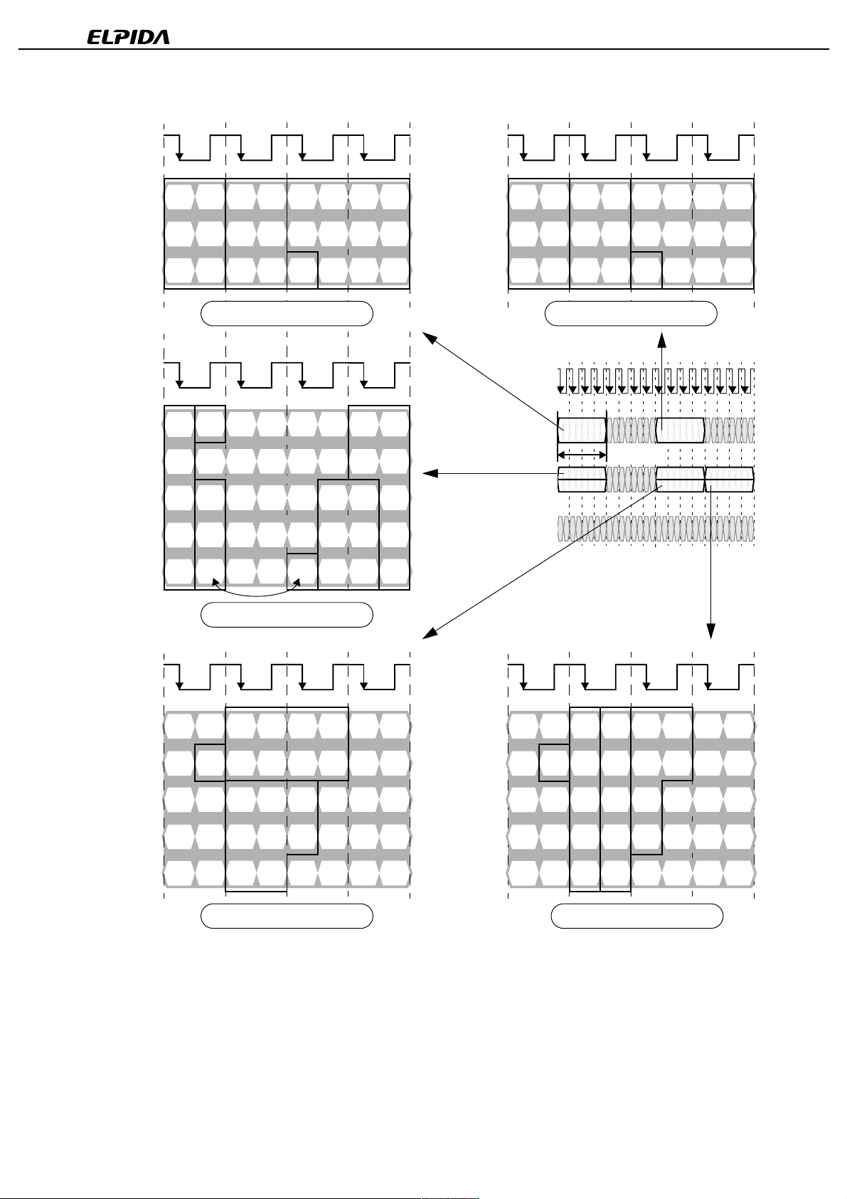
Figure 2-1 Packet Formats
µµµµ
PD488588FF-C80-40
CTM/CFM
ROW2
ROW1
ROW0
CTM/CFM
COL4
COL3
COL2
COL1
T
0
DR2 BR0 BR3 RsvR R8 R5
DR4T
DR1 BR1 BR4 RsvR R7 R4 R1
DR4F
DR0 BR2 RsvB AV=1 R6 R3 R0
DR3
T
1
T
2
ROWA Packet
T
0
S=1
DC4
DC3
COP1 RsvB BC2 C2
DC2
COP0 BC4 BC1 C1
DC1
T
1
T
2
T
3
R2
T
3
C4
C6
C5 C3
CTM/CFM
ROW2
ROW1
ROW0
CTM/CFM
ROW2
..ROW0
COL4
..COL0
DQA8..0
DQB8..0
T
8
DR2 BR0 BR3 ROP10ROP8ROP5
DR4T
DR1 BR1 BR4 ROP9ROP7ROP4ROP1
DR4F
DR0 BR2 RsvB AV=0 ROP6ROP3ROP0
DR3
T
9
T
10
ROWR Packet
T
0
T
T
1
ACT a0
WR b1
T
T
4
2
3
T
T
5
6
t
PACKET
T
7
T
T
8
PRER c0
T
11
ROP2
T
T
T
9
10
T
T
11
T
12
13
14
15
PREX d0MSK (b1)
COL0
CTM/CFM
COL4
COL3
COL2
COL1
COL0
COP2 COP3 BC3 BC0 C0
DC0
COLC Packet
T
8
T
9
T
10
T
11
T
12
T
13
CTM/CFM
Note1
MA7 MA5 MA3 MA1
S=1
M=1 MA6 MA4 MA2 MA0
MB7 MB4 MB1
MB6 MB3 MB0
MB5 MB2
COL4
COL3
COL2
COL1
COL0
COLM Packet
Notes 1. The COLM is associated with a previous COLC, and is aligned with the present COLC, indicated
by the Start bit (S=1) position.
2. The COLX is aligned with the present COLC, indicates by the Start bit (S=1) position.
Note2
DX4 XOP4 RsvB BX1
S=1
M=0 DX3 XOP3 BX4 BX0
DX2 XOP2 BX3
DX1 XOP1 BX2
DX0 XOP0
COLX Packet
T
14
T
15
Data Sheet E0251N20 (Ver. 2.0)
11
µµµµ
PD488588FF-C80-40
3. Field Encoding Summary
Table 3-1 shows how the six device address bits are decoded for the ROWA and ROWR packets. The DR4T and
DR4F encoding merges a fifth device bit with a framing bit. When neither bit is asserted, the device is not selected.
Note that a broadcast operation is indicated when both bits are set. Broadcast operation would typically be used for
refresh and power management commands. If the device is selected, the DM (DeviceMatch) signal is asserted and
an ACT or ROP command is performed.
Table 3-1 Device Field Encodings for ROWA Packet and ROWR Packet
DR4T DR4F Device Selection Device Match signal (DM)
1 1 All devices (broadcas t ) DM is set to 1
0 1 One device selected DM is set to 1 if {DEVID4..DEVID0} == {0, DR3..DR0} else DM is set to 0
1 0 One device selected DM is set to 1 if {DEVID4..DEVID0} == {1, DR3..DR0} else DM is set to 0
0 0 No packet present DM is set t o 0
Table 3-2 shows the encodings of the remaining fields of the ROWA and ROWR packets. An ROWA packet is
specified by asserting the AV bit. This causes the specified row of the specified bank of this device to be loaded into
the associated sense amps.
An ROWR packet is specified when AV is not asserted. An 11 bit opcode field encodes a command for one of the
banks of this device. The PRER command causes a bank and its two associated sense amps to precharge, so
another row or an adjacent bank may be activated.
The REFA (refresh-activate) command is similar to the ACT command, except the row address comes from an
internal register REFR, and REFR is incremented at the largest bank address. The REFP (refresh-precharge)
command is identical to a PRER command.
The NAPR, NAPRC, PDNR, ATTN, and RLXR commands are used for managing the power dissipation of the
RDRAM and are described in more detail in “23. Power State Management”. The TCEN and TCAL commands are
used to adjust the output driver slew rate and they are described in more detail in “25. Current and Temperature
Control”.
Table 3-2 ROWA Packet and ROWR Packet Field Encodings
DM AV ROP10..ROP0 Field Name Command Description
Note1
10 9 8 7 6 5 4 3 2 :
0 — — — — — — — — — --- — No operation.
1 1 Row address ACT Activate row R8..R0 of bank BR4..B R0 of device and move device to
1 0 1 1 0 0 0 x
1 0 0 0 0 1 1 0 0 x 000 REFA Refresh (activate) row REFR8..RE F R0 of bank BR3..BR0 of device.
1 0 1 0 1 0 1 0 0 x 000 REFP Precharge bank BR4..BR0 of this device after RE FA (see Figure 24-1).
1 0 x x 0 0 0 0 1 x 000 PDNR Move this device into the powerdown (PDN) power state (see figure 23-3).
1 0 x x 0 0 0 1 0 x 000 NAPR Move this device into the nap (NAP) power state (see Figure 23-3).
1 0 x x 0 0 0 1 1 x 000 NAPRC Move this device into the nap (NAP) power state conditionally.
1 0 x x x x x x x 0 000
1 0 x x x x x x x 1 000 RLXR Move this device into the standby (STBY) power state (see Figure 23-2).
1 0 0 0 0 0 0 0 0 x 001 TCAL Temperature calibrate this dev i ce (see figure 25-2).
1 0 0 0 0 0 0 0 0 x 010 TCEN Temperature calibrate/enable thi s device (see Figure 25-2).
1 0 0 0 0 0 0 0 0 0 000 NOROP No operation.
Notes 1. The DM (Device Match s i gnal ) value is determined by the DR4T, DR4F, DR3..DR0 field of the ROWA and ROWR packet s.
See Table 3-1.
2. The ATTN command does not cause a RLX-to-A TTN transition for a broadcast operati on (DR4T/ DR4F=1/1).
3. An “x” entry indicates which com m ands may be combined. For instance, the three commands PRER/ NA PRC/RLXR may
be specified in one ROP value (011000111000).
Note3
x x 000 PRER Precharge bank BR4..BR0 of t hi s device.
0
Note2
ATTN
Note2
ATTN
Increment REFR if BR4.. B R0=11111 (see Figure 24-1).
Move this device int o the attention (ATTN) power state (see Fi gure 23-1).
.
12
Data Sheet E0251N20 (Ver. 2.0)
µµµµ
PD488588FF-C80-40
Table 3-3 shows the COP field encoding. The device must be in the ATTN power state in order to receive COLC
packets. The COLC packet is used primarily to specify RD (read) and WR (write) commands. Retire operations
(moving data from the write buffer to a sense amp) happen automatically. See Figure 15-1 for a more detailed
description.
The COLC packet can also specify a PREC command, which precharges a bank and its associated sense amps.
The RDA/WRA commands are equivalent to a combining RD/WR with a PREC. RLXC (relax) performs a power mode
transition. See 23. Power State Management.
Table 3-3 COLC Packet Field Encodings
S DC4..DC0
(select device)
0 - - - - - - - - - — No operation.
1 /= (DEVID4. .0) - - - - - — Retire write buffer of this device.
1 == (DEVID4..0)
1 == (DEVID4..0) x001 WR Retire write buff er of this device, then write column C6..C0 of bank
1 == (DEVID4..0) x010 RSRV Reserved, no operation.
1 == (DEVID4..0) x011 RD Read column C6.. C0 of bank BC4..BC0 of this dev i ce.
1 == (DEVID4..0) x100 PREC Retire write buffer of this device, then precharge bank BC4..BC0 (see
1 == (DEVID4..0) x101 WRA Same as WR, but precharge bank B C4..BC0 after write buffer (wit h new
1 == (DEVID4..0) x110 RSRV Reserved, no operation.
1 == (DEVID4.. 0) x111 RDA Same as RD, but precharge bank BC4..BC0 afterward.
1 == (DEVID4..0) 1xxx RLXC Move this device into the standby (STBY) power state (see Figure 23-2).
COP3..0 Name Command Description
Note1
Note2
x000
NOCOP Retire write buffer of this device.
BC4..BC0 to write buffer.
Figure 12-2).
data) is retired.
Notes 1. “/=” means not equal, “==” means equal.
2. An “x” entry indicates which commands may be combined. For instance, the two commands WR/RLXC
may be specified in one COP value(1001).
Table 3-4 shows the COLM and COLX field encodings. The M bit is asserted to specify a COLM packet with two 8
bit bytemask fields MA and MB. If the M bit is not asserted, an COLX is specified. It has device and bank address
fields, and an opcode field. The primary use of the COLX packet is to permit an independent PREX (precharge)
command to be specified without consuming control bandwidth on the ROW pins. It is also used for the CAL
(calibrate) and SAM (sample) current control commands (see 25. Current and Temperature Control), and for the
RLXX power mode command (see 23. Power State Management).
Table 3-4 COLM Packet and COLX Packet Field Encodings
M DX4..DX0
(select device)
1 - - - - - MSK MB/MA bytemasks used by WR/WRA.
0 /= (DEVID4..0) - — No operation.
0 == (DEVID4..0) 00000 NOXOP No operation.
0 == (DEVID4..0)
0 == (DEVID4.. 0) x10x0 CAL Calibrate (drive) IOL current for this devic e (see Figure 25-1).
0 == (DEVID4..0) x11x0 CAL / SAM Calibrate (drive) and Sample (update) IOL current for this devic e (see Figure 25-1).
0 == (DEVID4..0) xxx10 RLXX Move this device into the standby (STBY) power state (s ee Fi gure 23-2).
0 == (DEVID4..0) xxxx1 RSRV Reserved, no operation.
XOP4..0 Name Command Description
Note
1xxx0
PREX Precharge bank BX4.. B X0 of this device (see Figure 12-2).
Note An “x” entry indicates which commands may be combined. For instance, the two commands PREX/RLXX
may be specified in one XOP value (10010).
Data Sheet E0251N20 (Ver. 2.0)
13
µµµµ
PD488588FF-C80-40
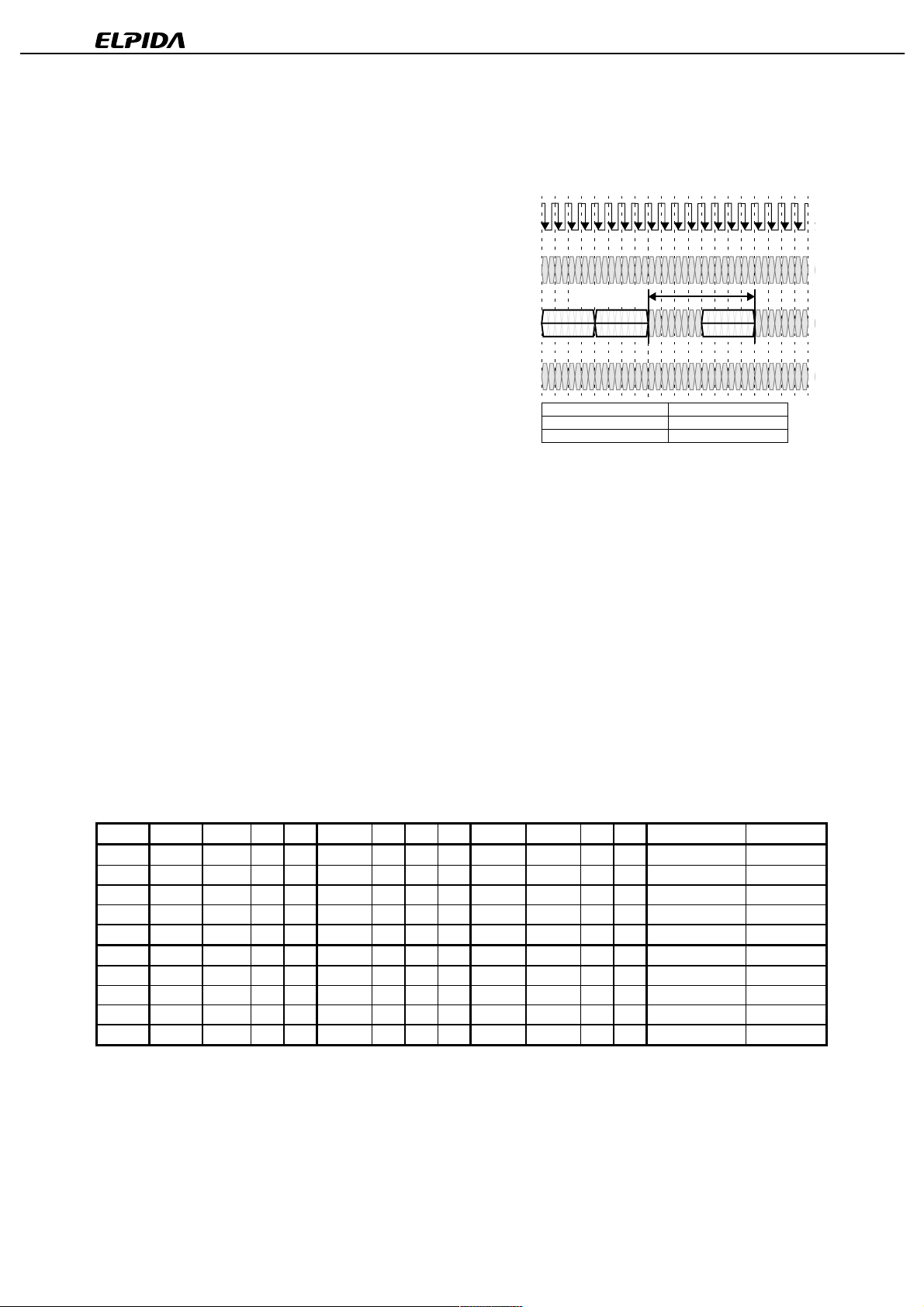
4. DQ Packet Timing
Figure 4-1 shows the timing relationship of COLC packets with D and Q data packets. This document uses a
specific convention for measuring time intervals between packets: all packets on the ROW and COL pins (ROWA,
ROWR, COLC, COLM, COLX) use the trailing edge of the packet as a reference point, and all packets on the
DQA/DQB pins (D and Q) use the leading edge of the packet as a reference point.
An RD or RDA command will transmit a dualoct of read data Q a time t
cycles of round-trip propagation delay on the Channel. The t
of values (7, 8, 9, 10, 11, or 12 t
). The value chosen depends upon the number of RDRAM devices on the
CYCLE
parameter may be programmed to a one of a range
CAC
Channel and the RDRAM timing bin. See Figure 22-1(5/7) “TPARM Register” for more information.
A WR or WRA command will receive a dualoct of write data D a time t
the round-trip propagation time of the Channel since the COLC and D packets are traveling in the same direction.
When a Q packet follows a D packet (shown in the left half of the figure), a gap (t
between them because the t
value is always less than the t
CWD
value. There will be no gap between the two COLC
CAC
packets with the WR and RD commands which schedule the D and Q packets.
When a D packet follows a Q packet (shown in the right half of the figure), no gap is needed between them because
the t
value is less than the t
CWD
value. However, a gap of t
CAC
CAC
- t
CWD
COLC packets with the RD WR commands by the controller so the Q and D packets do not overlap.
Figure 4-1 Read (Q) and Write (D) Data Packet - Timing for t
later. This time includes one to five
CAC
later. This time does not need to include
CWD
CAC-tCWD
) will automatically appear
or greater must be inserted between the
CAC
= 7,8,9,10,11 or 12 tCYCLE
T
T
T
T
T
1
2
3
0
4
T
T
T
T
5
6
7
T
T
8
T
T
9
T
T
10
11
T
12
16
T
13
14
15
T
T
T
T
17
18
19
20
T
T
T
T
21
22
23
T
T
24
T
T
25
T
T
26
27
T
28
32
T
29
30
31
T
T
T
T
33
34
35
36
T
T
T
T
37
38
39
T
T
41
40
T
T
T
T
42
43
T
45
46
47
44
CTM/CFM
ROW2
..ROW0
COL4
..COL0
DQA8..0
This gap on the DQA/DQB pins appears automatically
t
CAC-tCWD
t
CWD
RD b1WR a1
D (a1)
•••
Q (b1)
This gap on the COL pins must be inserted by the controller
t
CAC-tCWD
•••
RD c1
WR d1
t
CWD
Q (c1)
D (d1)
DQB8..0
t
CAC
•••
•••
t
CAC
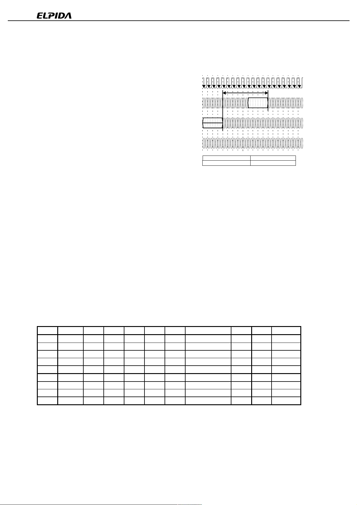
5. COLM Packet to D Packet Mapping
Figure 5-1 shows a write operation initiated by a WR command in a COLC packet. If a subset of the 16 bytes of
write data are to be written, then a COLM packet is transmitted on the COL pins a time t
containing the WR command. The M bit of the COLM packet is set to indicate that it contains the MA and MB mask
fields. Note that this COLM packet is aligned with the COLC packet which causes the write buffer to be retired. See
Figure 15-1 for more details.
If all 16 bytes of the D data packet are to be written, then no further control information is required. The packet slot
that would have been used by the COLM packet (t
after the COLC packet) is available to be used as an COLX
RTR
packet. This could be used for a PREX precharge command or for a housekeeping command (this case is not
shown). The M bit is not asserted in an COLX packet and causes all 16 bytes of the previous WR to be written
unconditionally. Note that a RD command will never need a COLM packet, and will always be able to use the COLX
packet option (a read operation has no need for the byte-write-enable control bits).
The figure 5-1 also shows the mapping between the MA and MB fields of the COLM packet and bytes of the D
packet on the DQA and DQB pins. Each mask bit controls whether a byte of data is written (=1) or not written (=0).
after the COLC packet
RTR
14
Data Sheet E0251N20 (Ver. 2.0)
µµµµ
PD488588FF-C80-40
Figure 5-1 Mapping between COLM Packet and D Packet for WR Command
CTM/CFM
ROW2
..ROW0
COL4
..COL0
DQA8..0
DQB8..0
CTM/CFM
COL4
COL3
COL2
T
0
T
T
T
T
1
2
3
T
T
T
T
5
6
7
4
T
T
9
8
T
T
10
T
T
11
T
12
16
T
13
14
15
T
T
T
T
17
18
19
20
T
T
T
T
21
22
23
T
T
25
24
T
T
26
T
T
T
29
30
27
31
28
PRER a2
t
RTR
retire (a1)WR a1
MSK (a1)
t
CWD
D (a1)
Transaction a: WR a0 = {Da,Ba,Ra} a1 = {Da,Ba,Ca1} a3 = {Da,Ba}
COLM Packet
T
17
T
18
T
19
T
20
T
19
CTM/CFM
MA7 MA5 MA3 MA1
M=1 MA6 MA4 MA2 MA0
MB7 MB4 MB1
DQB8
DQB7
•
•
•
DB17 DB26 DB35 DB45 DB53 DB62
DB8
DB16 DB25 DB34 DB44 DB52 DB61 DB70
DB7
T
T
32
ACT b0ACT a0
T
T
33
34
D Packet
T
20
T
35
36
T
T
T
T
37
38
39
40
T
21
T
T
41
T
T
42
T
T
43
T
45
46
47
44
T
22
DB71
COL1
COL0
When M=1, the MA and MB
fields control writing of
individual data bytes.
When M=0, all data bytes are
written unconditionally.
MB6 MB3 MB0
MB5 MB2
Each bit of the MB7..MB0 field
controls writing (=1) or no writing
(=0) of the indicated DB bits when
the M bit of the COLM packet is one.
Each bit of the MA7..MA0 field
controls writing (=1) or no writing
(=0) of the indicated DA bits when
the M bit of the COLM packet is one.
DQB1
DQB0
DQA8
DQA7
•
•
•
DQA1
DQA0
DB10 DB19 DB28 DB37 DB46 DB55 DB64
DB1
DB9 DB18 DB27 DB36 DB45 DB54 DB63
DB0
MB0
MB1
MB2
MB3
MB4
MB5
DA17 DA26 DA35 DA45 DA53 DA62
DA8
DA16 DA25 DA34 DA44 DA52 DA61 DA70
DA7
DA10 DA19 DA28 DA37 DA46 DA55 DA64
DA1
DA9 DA18 DA27 DA36 DA45 DA54 DA63
DA0
MA0
MA1
MA2
MA3
MA4
MA5
MB6
MA6
MB7
DA71
MA7
Data Sheet E0251N20 (Ver. 2.0)
15
µµµµ
PD488588FF-C80-40
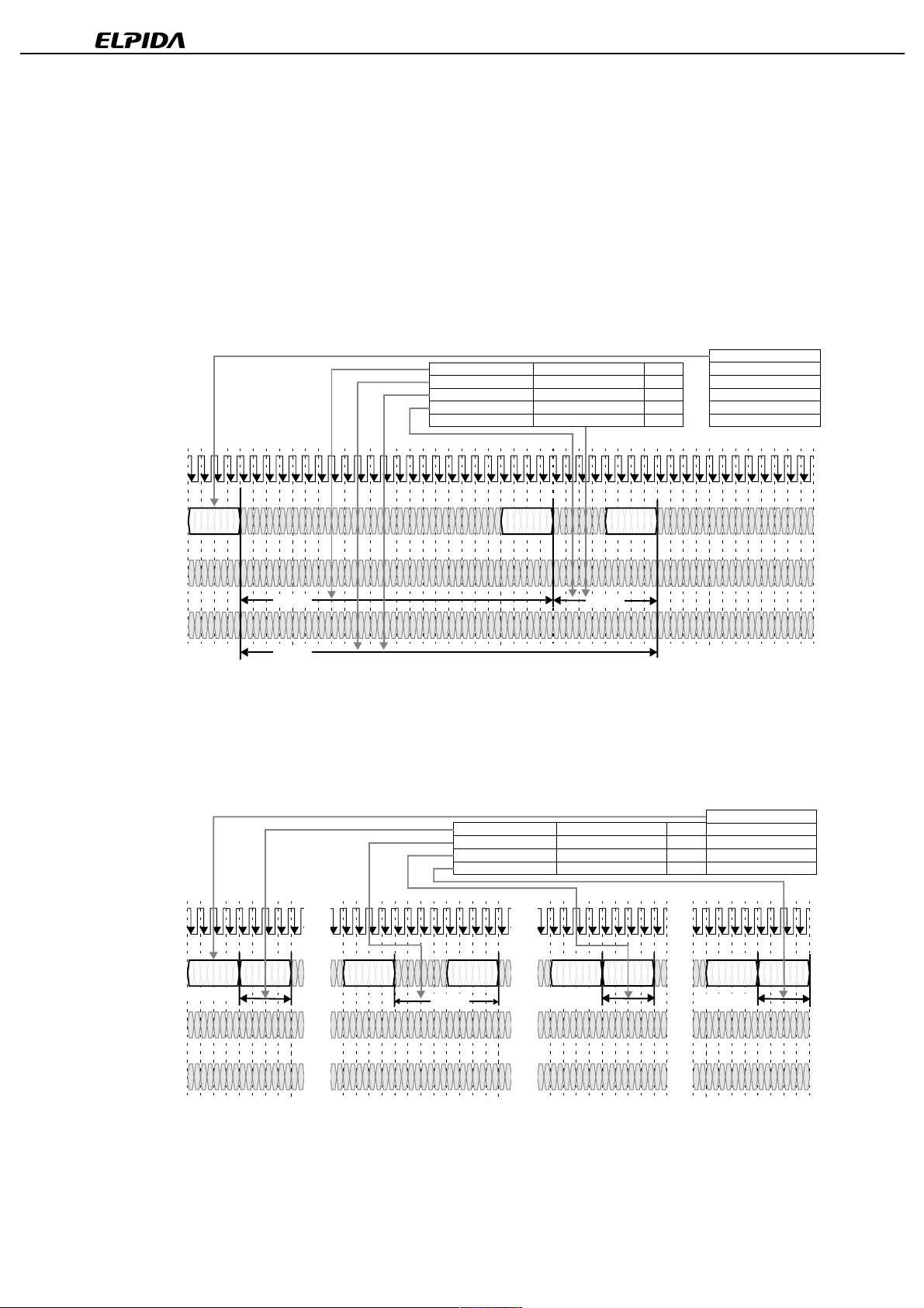
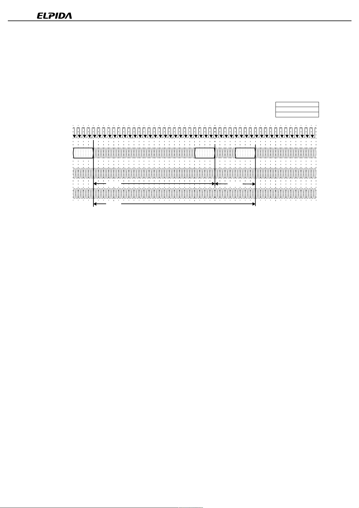
6. ROW-to-ROW Packet Interaction
Figure 6-1 shows two packets on the ROW pins separated by an interval t
contents. No other ROW packets are sent to banks {Ba, Ba+1, Ba-1} between packet “a” and packet “b” unless
noted otherwise.
Figure 6-1 ROW-to-ROW Packet Interaction - Timing
which depends upon the packet
RRDELAY
T
0
T
T
T
T
1
2
3
4
T
T
T
T
5
6
7
8
T
T
9
T
T
10
T
T
11
T
12
16
T
13
14
15
T17T18T
T
19
CTM/CFM
t
ROW2
ROPa a0 ROPb b0
RRDELAY
..ROW0
COL4
..COL0
DQA8..0
DQB8..0
Transaction a: ROPa
Transaction b: ROPb
Table 6-1 summarizes the t
RRDELAY
values for all possible cases.
Cases RR1 through RR4 show two successive ACT commands. In case RR1, there is no restriction since the ACT
commands are to different devices. In case RR2, the t
RR
banks. Cases RR3 and RR4 are illegal (as shown) since bank Ba needs to be precharged. If a PRER to Ba, Ba+1,
or Ba-1 is inserted, t
RRDELAY
is tRC (t
to the PRER command, and tRP to the next ACT).
RAS
Cases RR5 through RR8 show an ACT command followed by a PRER command. In cases RR5 and RR6, there are
no restrictions since the commands are to different devices or to non-adjacent banks of the same device. In cases
RR7 and RR8, the t
restriction means the activated bank must wait before it can be precharged.
RAS
Cases RR9 through RR12 show a PRER command followed by an ACT command. In cases RR9 and RR10, there
are essentially no restrictions since the commands are to different devices or to non-adjacent banks of the same
device. RR10a and RR10b depend upon whether a bracketed bank (Ba+-1) is precharged or activated. In cases
RR11 and RR12, the same and adjacent banks must all wait t
being activated.
Cases RR13 through RR16 summarize the combinations of two successive PRER commands. In case RR13 there
is no restriction since two devices are addressed. In RR14, t
RR15 and RR16, the same bank or an adjacent bank may be given repeated PRER commands with only the t
restriction.
Two adjacent banks can’t be activate simultaneously. A precharge command to one bank will thus affect the state of
the adjacent banks (and sense amps). If bank Ba is activate and a PRER is directed to Ba, then bank Ba will be
precharged along with sense amps Ba-1/Ba and Ba/Ba+1. If bank Ba+1 is activate and a PRER is directed to Ba,
then bank Ba+1 will be precharged along with sense amps Ba/Ba+1 and Ba+1/Ba+2. If bank Ba-1 is activate and a
PRER is directed to Ba, then bank Ba-1 will be precharged along with sense amps Ba/Ba-1 and Ba-1/Ba-2.
A ROW packet may contain commands other than ACT or PRER. The REFA and REFP commands are equivalent
to ACT and PRER for interaction analysis purposes. The interaction rules of the NAPR, NAPRC, PDNR, RLXR,
ATTN, TCAL, and TCEN commands are discussed in later section (see Table 3-2 for cross-ref).
a0 = {Da,Ba,Ra}
b0= {Db,Bb,Rb}
restriction applies to the same device with non-adjacent
for the sense amp and bank to precharge before
RP
applies, since the same device is addressed. In
PP
PP
16
Data Sheet E0251N20 (Ver. 2.0)
µµµµ
PD488588FF-C80-40
Table 6-1 ROW-to-ROW Packet Interaction - Rules
Case # ROPa Da Ba Ra ROPb Db Bb Rb t
RR1 ACT Da Ba Ra ACT /= Da xxxx x..x t
Example
RRDELAY
Figure 10-2
PACKET
RR2 ACT Da Ba Ra ACT == Da /= {Ba, Ba+1, Ba-1} x..x tRR Figure 10-2
RR3 ACT Da Ba Ra ACT == Da == {Ba+1, Ba-1} x..x t
RR4 ACT Da Ba Ra ACT == Da == {Ba} x..x t
RR5 ACT Da Ba Ra PRER /= Da xxxx x..x t
RR6 ACT Da Ba Ra PRER == Da /= {Ba, Ba+1, Ba-1} x..x t
RR7 ACT Da Ba Ra PRER == Da == {Ba+1, Ba -1} x..x t
RR8 ACT Da Ba Ra PRER == Da == {Ba} x..x t
RR9 PRER Da Ba Ra ACT /= Da xxxx x..x t
RR10 PRER Da Ba Ra ACT == Da /= {Ba, Ba+-1, Ba+-2} x..x t
RR10a PRER Da Ba Ra ACT == Da == {Ba+2} x..x t
RR10b PRER Da Ba Ra ACT == Da == {Ba-2} x..x t
- illegal unless PRER to Ba / Ba+1 / Ba-1 Figure 10-1
RC
- illegal unless PRER to Ba / Ba+1 / Ba-1 Figure 10-1
RC
Figure 10-2
PACKET
Figure 10-2
PACKET
Figure 10-1
RAS
Figure 13-1
RAS
Figure 10-3
PACKET
Figure 10-3
PACKET
PACKET/tRP
PACKET/tRP
if Ba+1 is precharged/acti vated.
if Ba-1 is precharged/activated.
RR11 PRER Da Ba Ra ACT == Da == {Ba+1, Ba-1} x..x tRP Figure 10-1
RR12 PRER Da Ba Ra ACT == Da == {Ba} x..x tRP Figure 10-1
RR13 PRER Da Ba Ra PRER /= Da xxxx x..x t
Figure 10-3
PACKET
RR14 PRER Da Ba Ra PRER == Da /= {Ba, Ba+1, Ba-1} x..x tPP Figure 10-3
RR15 PRER Da Ba Ra PRER == Da == {Ba+1, Ba-1} x..x tPP Figure 10-3
RR16 PRER Da Ba Ra PRER == Da == {Ba} x..x tPP Figure 10-3
Data Sheet E0251N20 (Ver. 2.0)
17
µµµµ
PD488588FF-C80-40
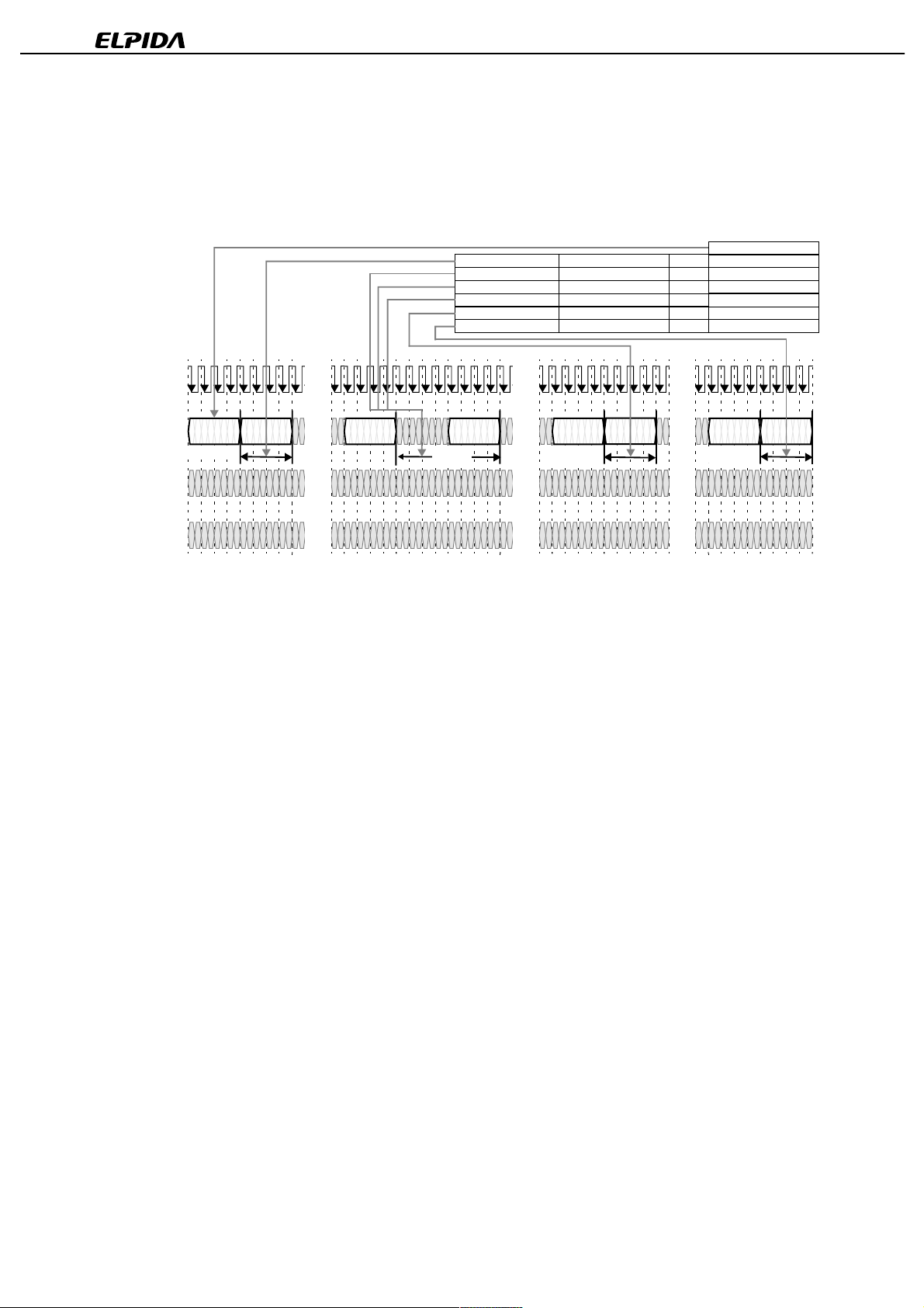
7. ROW-to-COL Packet Interaction
Figure 7-1 shows two packets on the ROW and COL pins. They must be separated by an interval t
depends upon the packet contents.
Figure 7-1 ROW-to-COL Packet Interaction- Timing
RCDELAY
which
T
0
T
T
T
T
1
2
3
4
T
T
T
T
5
6
7
8
T
T
9
T
T
10
T
T
11
T
12
16
T
13
14
15
T17T18T
T
19
CTM/CFM
t
ROW2
ROPa a0
RCDELAY
..ROW0
COL4
COPb b1
..COL0
DQA8..0
DQB8..0
Transaction a: ROPa
Transaction b: COPb
Table 7-1 summarizes the t
RCDELAY
values for all possible cases. Note that if the COL packet is earlier than the
ROW packet, it is considered a COL-to-ROW packet interaction.
Cases RC1 through RC5 summarize the rules when the ROW packet has an ACT command. Figure 13-1 and
Figure 14-1 show examples of RC5 - an activation followed by a read or write. RC4 is an illegal situation, since a
read or write of a precharged banks is being attempted (remember that for a bank to be activated, adjacent banks
must be precharged). In cases RC1, RC2, and RC3, there is no interaction of the ROW and COL packets.
Cases RC6 through RC8 summarize the rules when the ROW packet has a PRER command. There is either no
interaction (RC6 through RC9) or an illegal situation with a read or write of a precharged bank (RC9).
The COL pins can also schedule a precharge operation with a RDA, WRA, or PREC command in a COLC packet or
a PREX command in a COLX packet. The constraints of these precharge operations may be converted to equivalent
PRER command constraints using the rules summarized in Figure 12-2.
Table 7-1 ROW-to-COL Packet Interaction - Rules
a0 = {Da,Ba,Ra}
b1= {Db,Bb,Cb1}
Case # ROPa Da Ba Ra COPb Db Bb Cb1 t
RCDELAY
Example
RC1 ACT Da Ba Ra NOCOP, RD, retire /= Da xxxx x..x 0
RC2 ACT Da Ba Ra NOCOP == Da xxxx x..x 0
RC3 ACT Da Ba Ra RD, retire == Da /= {Ba, Ba+1, Ba-1} x..x 0
RC4 AC T Da Ba Ra RD, retire == Da == {Ba +1, Ba- 1} x..x Illegal
RC5 ACT Da Ba Ra RD, retire == Da == {Ba} x..x t
Figure 13-1
RCD
RC6 PRER Da Ba Ra NOCOP, RD, retire /= Da xxxx x..x 0
RC7 PRER Da Ba Ra NOCOP == Da xxxx x..x 0
RC8 PRER Da Ba Ra RD, retire == Da /= {Ba, Ba+1, Ba-1} x..x 0
RC9 PR ER D a Ba Ra RD, retire == Da == {Ba+ 1, Ba-1} x..x Illegal
18
Data Sheet E0251N20 (Ver. 2.0)
µµµµ
PD488588FF-C80-40
8. COL-to-COL Packet Interaction
Figure 8-1 shows three arbitrary packets on the
COL pins. Packets “b” and “c” must be separated by
an interval t
CCDELAY
which depends upon the
command and address values in all three packets.
Table 8-1 summarizes the t
CCDELAY
values for all
possible cases.
Cases CC1 through CC5 summarize the rules for
every situation other than the case when COPb is a
WR command and COPc is a RD command. In
CC3, when a RD command is followed by a WR
command, a gap of t
CAC - tCWD
must be inserted
between the two COL packets. See Figure 4-1 for
more explanation of why this gap is needed. For
cases CC1, CC2, CC4, and CC5, there is no
restriction (t
CCDELAY
is tCC).
In cases CC6 through CC10, COPb is a WR command and COPc is a RD command. The t
between these two packets depends upon the command and address in the packet with COPa. In particular, in case
CC6 when there is WR-WR-RD command sequence directed to the same device, a gap will be needed between the
packets with COPb and COPc. The gap will need a COLC packet with a NOCOP command directed to any device in
order to force an automatic retire to take place. Figure 15-2 (right) provides a more detailed explanation of this case.
In case CC10, there is a RD-WR-RD sequence directed to the same device. If a prior write to the same device is
unretired when COPa is issued, then a gap will be needed between the packets with COPb and COPc as in case
CC6. The gap will need a COLC packet with a NOCOP command directed to any device in order to force an
automatic retire to take place.
Cases CC7, CC8, and CC9 have no restriction (t
CCDELAY
For the purposes of analyzing COL-to-ROW interactions, the PREC, WRA, and RDA commands of the COLC
packet are equivalent to the NOCOP, WR, and RD commands. These commands also cause a precharge operation
PREC to take place. This precharge may be converted to an equivalent PRER command on the ROW pins using the
rules summarized in Figure 12-2.
Table 8-1 COL-to-COL Packet Interaction - Rules
Figure 8-1 COL-to-COL Packet Interaction- Timing
T
0
T
T
T
T
1
2
3
4
T
T
T
T
5
6
7
T
T
8
T
T
9
10
T
T
11
T
13
14
15
12
CTM/CFM
ROW2
..ROW0
t
CCDELAY
COL4
COPa a1
COPb b1
COPc c1
..COL0
DQA8..0
DQB8..0
is tCC).
Transaction a: COPa
Transaction b: COPb
Transaction c: COPc
a1 = {Da,Ba,Ca1}
b1 = {Db,Bb,Cb1}
c1 = {Dc,Bc,Cc1}
CCDELAY
value needed
T
T17T18T
16
T
19
Case # COPa Da Ba Ca1 COPb Db Bb Cb1 COPc Dc Bc Cc1 t
Example
CCDELAY
CC1 xxxx xxxxx x..x x..x NOCOP Db Bb Cb1 xxxx xxxxx x..x x..x tCC
CC2 xxxx xxxxx x..x x..x RD, WR Db Bb Cb1 NOCOP xxxxx x..x x..x tCC
CC3 xxxx xxxxx x..x x..x RD Db Bb Cb1 WR xxxxx x..x x..x t
CC + tCAC - tCWD
Figure 4-1
CC4 xxxx xxxxx x..x x..x RD Db Bb Cb1 RD xxxxx x..x x..x tCC Figure 13-1
CC5 xxxx xxxxx x..x x..x WR Db Bb Cb1 WR xxxxx x..x x..x tCC Figure 14-1
CC6 WR == Db x x..x WR Db Bb Cb1 RD == Db x..x x..x t
Figure 15-1
RTR
CC7 WR == Db x x..x WR Db Bb Cb1 RD /= Db x..x x. .x tCC
CC8 WR /= Db x x..x WR Db Bb Cb1 RD == Db x.. x x.. x tCC
CC9 NOCOP == Db x x.. x WR Db Bb Cb1 RD == Db x..x x..x tCC
CC10 RD == Db x x..x WR Db Bb Cb1 RD == Db x..x x..x tCC
Data Sheet E0251N20 (Ver. 2.0)
19
µµµµ
PD488588FF-C80-40
9. COL-to-ROW Packet Interaction
Figure 9-1 shows arbitrary packets on the COL
and ROW pins. They must be separated by an
interval t
CRDELAY
which depends upon the
command and address values in the packets.
Table 9-1 summarizes the t
CRDELAY
value for all
possible cases.
Cases CR1, CR2, CR3, and CR9 show no
interaction between the COL and ROW packets,
either because one of the commands is a NOP or
because the packets are directed to different
devices or to non-adjacent banks.
Case CR4 is illegal because an already-activated
bank is to be re-activated without being
precharged. Case CR5 is illegal because an
adjacent bank can’t be activated or precharged
until bank Ba is precharged first.
In case CR6, the COLC packet contains a RD command, and the ROW packet contains a PRER command for the
same bank. The t
parameter specifies the required spacing.
RDP
Likewise, in case CR7, the COLC packet causes an automatic retire to take place, and the ROW packet contains a
PRER command for the same bank. The t
parameter specifies the required spacing.
RTP
Case CR8 is labeled “Hazardous” because a WR command should always be followed by an automatic retire before
a precharge is scheduled. Figure 15-3 shows an example of what can happen when the retire is not able to happen
before the precharge.
For the purposes of analyzing COL-to-ROW interactions, the PREC, WRA, and RDA commands of the COLC
packet are equivalent to the NOCOP, WR, and RD commands. These commands also cause a precharge operation
to take place. This precharge may converted to an equivalent PRER command on the ROW pins using the rules
summarized in Figure 12-2.
A ROW packet may contain commands other than ACT or PRER. The REFA and REFP commands are equivalent
to ACT and PRER for interaction analysis purposes. The interaction rules of the NAPR, PDNR, and RLXR
commands are discussed in a later section.
Table 9-1 COL-to-ROW Packet Interaction - Rules
Figure 9-1 COL-to-ROW Packet Interaction- Timing
T
T
T
T
T
1
2
3
0
T
T
T
T
5
6
7
4
T
T
8
T
T
9
10
T
T
T
T
13
11
12
T17T18T
14
15
16
CTM/CFM
t
CRDELAY
ROW2
ROPb b0
..ROW0
COL4
COPa a1
..COL0
DQA8..0
DQB8..0
Transaction a: COPa
Transaction b: ROPb
a1= {Da,Ba,Ca1}
b0= {Db,Bb,Rb}
T
19
Case # COPa Da Ba Ca1 ROPb Db B b Rb t
CRDELAY
Example
CR1 NOCOP Da Ba Ca1 x..x xxxxx xxxxx x..x 0
CR2 RD/WR Da Ba Ca1 x..x /= Da xxxxx x..x 0
CR3 RD/WR Da Ba Ca1 x..x == Da /= {Ba, Ba+1, Ba-1} x..x 0
CR4 RD/WR Da Ba Ca1 ACT == Da == {Ba} x..x Illegal
CR5 RD/WR Da Ba Ca1 ACT == Da == {Ba+1, Ba -1} x..x Ill egal
CR6 RD Da Ba Ca1 PRER == Da == {Ba, Ba+1, Ba-1} x..x t
Note 1
CR7
CR8
retire
WR
Da Ba Ca1 PRER == Da == {Ba, Ba+1, Ba-1} x..x t
Note 2
Da B a Ca1 PRER == Da == {Ba, Ba+1, Ba-1} x..x 0 Figure 15-3
Figure 13-1
RDP
Figure 14-1
RTP
CR9 xxxx Da Ba Ca1 NOROP xxxxx xxxxx x..x 0
Notes 1. This is any command which permits the write buffer of device Da to retire (see Table 3-3). “Ba” is the bank
address in the write buffer.
2. This situation is hazardous because the write buffer will be left unretired while the targeted bank is
precharged. See Figure 15-3.
20
Data Sheet E0251N20 (Ver. 2.0)
µµµµ
PD488588FF-C80-40
10. ROW-to-ROW Examples
Figure 10-1 shows examples of some of the ROW-to-ROW packet spacings from Table 6-1. A complete sequence
of activate and precharge commands is directed to a bank. The RR8 and RR12 rules apply to this sequence. In
addition to satisfying the t
must also satisfy the t
RC
RAS
timing parameter (RR4).
and t
timing parameters, the separation between ACT commands to the same bank
RP
When a bank is activated, it is necessary for adjacent banks to remain precharged. As a result, the adjacent banks
will also satisfy parallel timing constraints; in the example, the RR11 and RR3 rules are analogous to the RR12 and
RR4 rules.
Figure 10-1 Row Packet Example
a0 = {Da,Ba,Ra}
Same Device Adjacent Bank RR7
Same Device Adjacent Bank RR11
T
0
T
T
T
T
1
2
3
4
T
T
T
T
5
6
7
T
T
8
T
T
9
T
T
10
T
11
15
12
T
13
14
T
T
T
T
17
18
19
16
20
T
T
T
T
21
22
23
T
T
24
T
T
25
T
T
26
27
T
28
32
T
29
30
31
T
T
33
T
T
34
T
T
37
35
36
a1 = {Da,Ba+1}
b0 = {Da,Ba+1,Rb}Same Device Adjacent Bank RR3
b0 = {Da,Ba,Rb}Same Device Same Bank RR4
b0 = {Da,Ba+1,Rb}
b0 = {Da,Ba,Rb}Same Device Same Bank RR12
T
T
T
T
41
38
42
39
40
T
T
T
T
T
45
46
43
47
44
CTM/CFM
ROW2
ACT a0 PRER a1
ACT b0
..ROW0
COL4
..COL0
t
RAS
t
RP
DQA8..0
DQB8..0
t
RC
Figure 10-2 shows examples of the ACT-to-ACT (RR1, RR2) and ACT-to-PRER (RR5, RR6) command spacings
from Table 6-1. In general, the commands in ROW packets may be spaced an interval t
apart unless they are
PACKET
directed to the same or adjacent banks or unless they are a similar command type (both PRER or both ACT)
directed to the same device.
Figure 10-2 Row Packet Example
Different Device Any Bank
Same Device Non-adjacent Bank
Different Device Any Bank
Same Device Non-adjacent Bank
T
0
T
T
T
T
1
2
3
T
T
T
T
5
6
7
4
T
T
8
T
T
9
T
T
10
T
11
15
12
16
T
13
14
T
T
T
T
17
18
19
T
T
T
T
21
22
23
20
T
T
24
T
T
25
T
T
26
T
27
31
28
32
T
29
30
T
T
33
T
T
T
37
34
35
36
RR1
RR2
RR5
RR6
T
38
T
39
a0 = {Da,Ba,Ra}
b0 = {Db,Bb,Rb}
c0 = {Da,Bc,Rc}
b0 = {Db,Bb,Rb}
c0 = {Da,Bc,Rc}
T
T
T
T
T
41
42
43
40
44
T
T
45
46
CTM/CFM
T
47
ROW2
..ROW0
COL4
..COL0
DQA8..0
DQB8..0
ACT a0 PRER b0
t
PACKET
t
RR
ACT c0
ACT a0ACT a0ACT b0 PRER c0
t
PACKET
Data Sheet E0251N20 (Ver. 2.0)
ACT a0
t
PACKET
21
µµµµ
PD488588FF-C80-40
Figure 10-3 shows examples of the PRER-to-PRER (RR13, RR14) and PRER-to-ACT (RR9, RR10) command
spacings from Table 6-1. The RR15 and RR16 cases (PRER-to-PRER to same or adjacent banks) are not shown,
but are similar to RR14. In general, the commands in ROW packets may be spaced an interval t
PACKET
apart unless
they are directed to the same or adjacent banks or unless they are a similar command type (both PRER or both ACT)
directed to the same device.
Figure 10-3 Row Packet Example
Different Device Any Bank
Same Device Non-adjacent Bank
RR13
RR14
a0 = {Da,Ba,Ra}
b0 = {Db,Bb,Rb}
c0 = {Da,Bc,Rc}
c0 = {Da,Ba,Rc}Same Device Ajacent Bank RR15
Different Device
Any Bank
Same Device Non-adjacent Bank
T
T
T
T
T
1
2
3
0
4
T
T
T
T
5
6
7
T
T
8
T
T
9
T
T
10
T
11
15
12
T
13
14
T
T
T
T
17
18
19
16
20
T
T
T
T
21
22
23
T
T
24
T
T
25
26
T
T
T
27
31
28
T
29
30
T
T
T
T
33
34
35
32
36
RR9
RR10
T
T
37
c0 = {Da,Ba+1Rc}Same Device Same Bank RR16
b0 = {Db,Bb,Rb}
c0 = {Da,Bc,Rc}
T
T
T
41
38
39
40
T
T
T
T
T
42
43
T
45
46
47
44
CTM/CFM
ROW2
..ROW0
PRER a0 ACT b0
t
PACKET
PRER c0
t
PP
PRER a0PRER a0PRER b0 ACT c0
t
PACKET
PRER a0
t
PACKET
COL4
..COL0
DQA8..0
DQB8..0
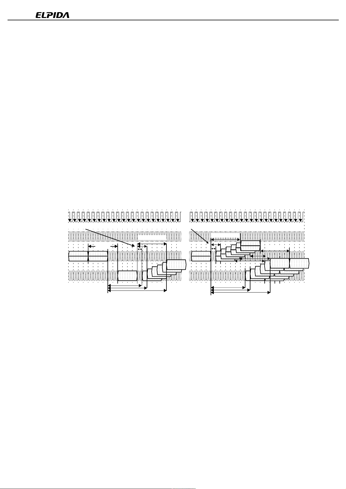
11. Row and Column Cycle Description
Activate: A row cycle begins with the activate (ACT) operation. The activation process is destructive; the act of
sensing the value of a bit in a bank’s storage cell transfers the bit to the sense amp, but leaves the original bit in the
storage cell with an incorrect value.
Restore: Because the activation process is destructive, a hidden operation called restore is automatically performed.
The restore operation rewrites the bits in the sense amp back into the storage cells of the activated row of the bank.
Read/Write: While the restore operation takes place, the sense amp may be read (RD) and written (WR) using
column operations. If new data is written into the sense amp, it is automatically forwarded to the storage cells of the
bank so the data in the activated row and the data in the sense amp remain identical.
Precharge: When both the restore operation and the column operations are completed, the sense amp and bank are
precharged (PRE). This leaves them in the proper state to begin another activate operation.
to complete. The hidden restore operation requires the
Intervals: The activate operation requires the interval t
interval t
t
RCD,MIN
- t
RAS,MIN
interval (if more than about four column operations are performed, this interval must be increased). The
precharge operation requires the interval t
to complete. Column read and write operations are also performed during the t
RCD,MIN
RP,MIN
Adjacent Banks: An RDRAM with a “s” designation (512K
RCD,MIN
to complete.
-
RAS,MIN
x 18 x 32s) indicates it contains “split banks”. This means
the sense amps are shared between two adjacent banks. The only exception is that sense amp 0, 15, 30, and 31 are
not shared. When a row in a bank is activated, the two adjacent sense amps are connected to (associated with) that
bank and are not available for use by the two adjacent banks. These two adjacent banks must remain precharged
while the selected bank goes through its activate, restore, read/write, and precharge operations.
For example (referring to the block diagram), if bank 5 is accessed, sense amp 4/5 and sense amp 5/6 will both be
loaded with one of the 512 rows (with 1,024 bytes loaded into each sense amp from the 2K byte row – 512 bytes to
the DQA side and 512 bytes to the DQB side). While this row from bank 5 is being accessed, no rows may be
accessed in banks 4 or 6 because of the sense amp sharing.
22
Data Sheet E0251N20 (Ver. 2.0)
µµµµ
PD488588FF-C80-40
12. Precharge Mechanisms
Figure 12-1 shows an example of precharge with the ROWR packet mechanism. The PRER command must occur
a time t
after the ACT command, and a time t
RAS
before the next ACT command. This timing will serve as a
RP
baseline against which the other precharge mechanisms can be compared.
Figure 12-1 Precharge via PRER Command in ROWR Packet
a0 = {Da,Ba,Ra}
a5 = {Da,Ba}
b0 = {Da,Ba,Rb}
T
0
T
T
T
T
1
2
3
4
T
T
T
T
5
6
7
T
T
8
T
T
9
T
T
10
11
T
T
13
14
15
12
T
T
T
T
17
18
19
16
20
T
T
T
T
21
22
23
T
T
24
T
T
25
T
T
26
27
T
28
32
T
29
30
31
T
T
T
T
33
34
35
36
T
T
T
T
37
38
39
T
T
40
T
T
41
T
T
42
T
45
46
43
47
44
CTM/CFM
ROW2
ACT a0 PRER a5
ACT b0
..ROW0
COL4
..COL0
t
RAS
t
RP
DQA8..0
DQB8..0
t
RC
Figure 12-2 (top) shows an example of precharge with a RDA command. A bank is activated with an ROWA packet
on the ROW pins. Then, a series of four dualocts are read with RD commands in COLC packets on the COL pins.
The fourth of these commands is a RDA, which causes the bank to automatically precharge when the final read has
finished. The timing of this automatic precharge is equivalent to a PRER command in an ROWR packet on the ROW
pins that is offset a time t
from the COLC packet with the RDA command. The RDA command should be treated
OFFP
as a RD command in a COLC packet as well as a simultaneous (but offset) PRER command in an ROWR packet
when analyzing interactions with other packets.
Figure 12-2 (middle) shows an example of precharge with a WRA command. As in the RDA example, a bank is
activated with an ROWA packet on the ROW pins. Then, two dualocts are written with WR commands in COLC
packets on the COL pins. The second of these commands is a WRA, which causes the bank to automatically
precharge when the final write has been retired. The timing of this automatic precharge is equivalent to a PRER
command in an ROWR packet on the ROW pins that is offset a time t
from the COLC packet that causes the
OFFP
automatic retire. The WRA command should be treated as a WR command in a COLC packet as well as a
simultaneous (but offset) PRER command in an ROWR packet when analyzing interactions with other packets. Note
that the automatic retire is triggered by a COLC packet a time t
after the COLC packet with the WR command
RTR
unless the second COLC contains a RD command to the same device. This is described in more detail in Figure 15-
1.
Figure 12-2 (bottom) shows an example of precharge with a PREX command in an COLX packet. A bank is
activated with an ROWA packet on the ROW pins. Then, a series of four dualocts are read with RD commands in
COLC packets on the COL pins. The fourth of these COLC packets includes an COLX packet with a PREX
command. This causes the bank to precharge with timing equivalent to a PRER command in an ROWR packet on
the ROW pins that is offset a time t
from the COLX packet with the PREX command.
OFFP
Data Sheet E0251N20 (Ver. 2.0)
23
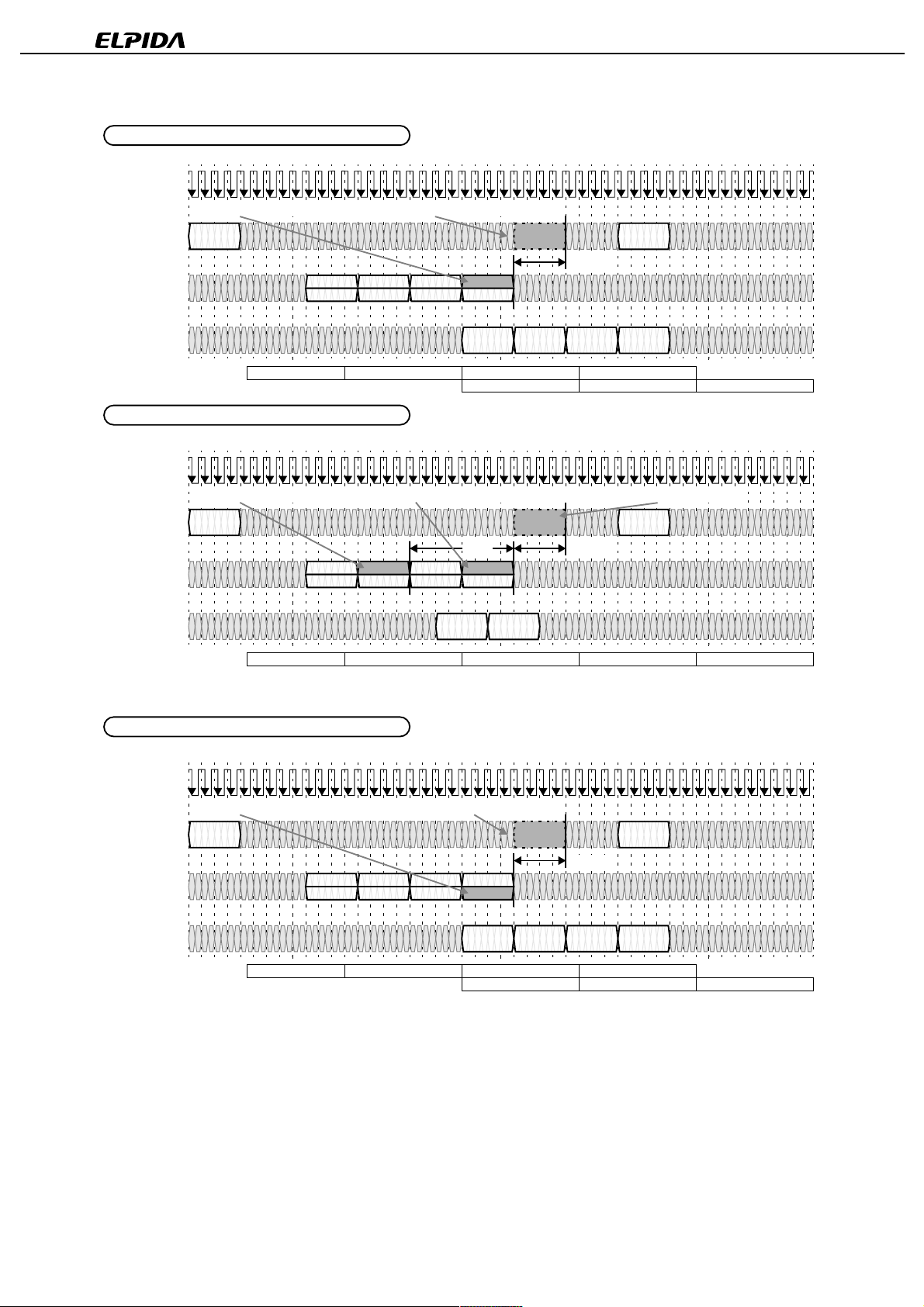
Figure 12-2 Offsets for Alternate Precharge Mechanisms
COLC Packet: RDA Precharge Offset
CTM/CFM
ROW2
..ROW0
COL4
..COL0
T
0
T
T
T
T
1
2
3
4
T
T
T
T
5
6
7
T
T
8
T
T
9
T
T
13
10
14
11
12
The RDA precharge is equivalent to a PRER command here
ACT a0
RD a1
RD a2
µµµµ
PD488588FF-C80-40
T
T
15
T
T
T
T
17
18
19
16
20
RD a3
T
T
21
RDA a4
T
T
22
23
T
25
24
PRER a5
T
T
T
T
T
26
27
T
T
29
30
31
28
32
T
T
T
T
33
34
35
T
T
T
T
37
38
39
36
T
T
40
T
T
41
42
T
T
T
45
46
43
47
44
ACT b0
t
OFFP
DQA8..0
DQB8..0
Transaction a: RD a0 = {Da,Ba,Ra}
COLC Packet: WDA Precharge Offset
CTM/CFM
ROW2
..ROW0
COL4
..COL0
DQA8..0
DQB8..0
T
0
T
T
T
T
1
2
3
4
T
T
T
T
5
6
7
T
T
8
T
T
9
T
T
10
11
T
13
14
15
12
The WRA precharge (triggered by the automatic retire) is equivalent to a PRER command here
WR a1
WRA a2 retire (a2)
Transaction a: WR a0 = {Da,Ba,Ra} a1 = {Da,Ba,Ca1} a2 = {Da,Ba,Ca2} a5 = {Da,Ba}
COLX Packet: PREX Precharge Offset
CTM/CFM
ROW2
..ROW0
COL4
..COL0
T
0
The PREX precharge command is equivalent to a PRER command here
T
T
1
ACT a0
T
T
2
3
4
T
T
T
T
5
6
7
T
T
8
T
9
RD a1
T
T
T
10
11
T
13
14
15
12
RD a2
T
T
16
retire (a1)
T
T
16
T
17
T
17
RD a3
Q (a2)Q (a1)
Q (a4)Q (a3)
a1 = {Da,Ba,Ca1} a2 = {Da,Ba,Ca2}
T
37
T
37
T
T
38
39
T
T
38
39
a5 = {Da,Ba}
T
T
T
T
41
42
43
40
T
T
T
T
41
42
43
40
T
T
T
45
46
47
44
T
T
T
45
46
47
44
a3 = {Da,Ba,Ca3} a4 = {Da,Ba,Ca4}
T
T
18
19
20
T
T
18
19
20
T
T
21
22
t
RTR
MSK (a2)MSK (a1)
T
T
21
22
RD a4
PREX a5
T
T
23
T
25
24
PRER a5
T
T
T
T
T
26
27
T
T
29
30
31
28
32
T
T
33
T
T
T
34
35
36
ACT b0ACT a0
t
OFFP
D (a2)D (a1)
T
T
23
T
25
24
PRER a5
T
T
T
T
T
26
27
T
T
29
30
31
28
32
T
T
33
T
T
T
34
35
36
ACT b0
t
OFFP
DQA8..0
DQB8..0
24
Transaction a: RD a0 = {Da,Ba,Ra}
Data Sheet E0251N20 (Ver. 2.0)
Q (a2)Q (a1)
Q (a4)Q (a3)
a1 = {Da,Ba,Ca1} a2 = {Da,Ba,Ca2}
a3 = {Da,Ba,Ca3} a4 = {Da,Ba,Ca4}
a5 = {Da,Ba}
 Loading...