

ELPIDA PD45128163G5-A75SU-9JF, PD45128163G5-A80SU-9JF Datasheet

PRELIMINARY DATA SHEET
MOS INTEGRATED CIRCUIT
PD45128163-SU
µµµµ
128M-bit Synchronous DRAM
4-bank, LVTTL
WTR (Wide Temperature Range)
Description
The µPD45128163 are high-speed 134,217,728-bit synchronous dynamic random-access memories, organized as
2,097,152 × 16 × 4 (word × bit × bank).
The synchronous DRAMs achieved high-speed data transfer using the pipeline architecture.
All inputs and outputs are synchronized with the positive edge of the clock.
The synchronous DRAMs are compatible with Low Voltage TTL (LVTTL).
These products are packaged in 54-pin TSOP (II).
Features
Fully Synchronous Dynamic RAM, with all signals referenced to a positive clock edge
•
• Pulsed interface
Possible to assert random column address in every cycle
•
• Quad internal banks controlled by BA0(A13) and BA1(A12)
Byte control by LDQM and UDQM
•
• Programmable Wrap sequence (Sequential / Interleave)
Programmable burst length (1, 2, 4, 8 and full page)
•
• Programmable /CAS latency (2 and 3)
A
Ambient temperature (T
•
• Automatic precharge and controlled precharge
CBR (Auto) refresh and self refresh
•
• ×16 organization
Single 3.3 V ± 0.3 V power supply
•
• LVTTL compatible inputs and outputs
4,096 refresh cycles / 64 ms
•
• Burst termination by Burst stop command and Precharge command
): −20 to + 70°C
The information in this document is subject to change without notice. Before using this document, please
confirm that this is the latest version.
Not all devices/types available in every country. Please check with local Elpida Memory, Inc. for
availability and additional information.
Document No. E0242N10 (Ver. 1.0)
Date Published December 2001 (K) Japa n
Elpida Memory, Inc. is a joint venture DRAM company of NEC Corporation and Hitachi, Ltd.

Ordering Information
µµµµ
PD45128163-SU
Part number
µ
PD45128163G5-A75SU-9JF 2M
µ
PD45128163G5-A80SU-9JF 125 (10.16mm (400))
Organization
(word × bit × bank)
16 × 4 133 54-pin Plastic TSOP (II)
×
Clock frequency
MHz (MAX.)
Package Note
Ambient temperature
T
A
= −20 to + 70°C
2
Preliminary Data Sheet E0242N10

Part Number
[ x16 ]
NEC Memory
Synchronous DRAM
Memory density
128 : 128M bits
µµµµ
PD45128163G5 - A75SU
µ
PD45128163-SU
Wide temperature
range
U : -20 to + 70°C
Organization
16 : x16
Number of banks
3 : 4 banks, LVTTL
Low Power
S : 0.6mA
Minimum cycle time
75 : 7.5 ns (133 MHz)
80 : 8 ns (125 MHz)
Low voltage
A : 3.3 V
Package
G5 : TSOP (II)
±
0.3 V
Preliminary Data Sheet E0242N10
3
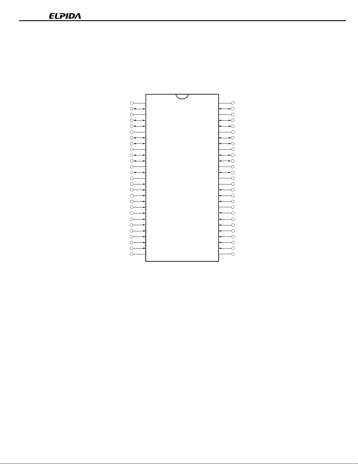
Pin Configurations
/xxx indicates active low signal.
BA0(A13)
BA1(A12)
PD45128163]
[
µµµµ
54-pin Plastic TSOP (II) (10.16mm (400))
2M words
16 bits
××××
V
DQ0
V
CC
DQ1
DQ2
SS
V
DQ3
DQ4
CC
V
DQ5
DQ6
V
SS
DQ7
V
LDQM
/WE
/CAS
/RAS
/CS
A10
A0
A1
A2
A3
V
CC
Q
Q
Q
Q
CC
CC
1
2
3
4
5
6
7
8
9
10
11
12
13
14
15
16
17
18
19
20
21
22
23
24
25
26
27
4 banks
××××
54
53
52
51
50
49
48
47
46
45
44
43
42
41
40
39
38
37
36
35
34
33
32
31
30
29
28
Vss
DQ15
VssQ
DQ14
DQ13
VccQ
DQ12
DQ11
VssQ
DQ10
DQ9
VccQ
DQ8
Vss
NC
UDQM
CLK
CKE
NC
A11
A9
A8
A7
A6
A5
A4
Vss
µµµµ
PD45128163-SU
Note
A0 to A11
: Address inputs
BA0(A13), BA1(A12) : Bank select
DQ0 to DQ15 : Data inputs / outputs
CLK : Clock input
CKE : Clock enable
/CS : Chip select
/RAS : Row address strobe
/CAS : Column address strobe
/WE : Write enable
LDQM : Lower DQ mask enable
UDQM : Upper DQ mask enable
CC
: Supply voltage
V
SS
: Ground
V
CC
Q : Supply voltage for DQ
V
SS
Q : Ground for DQ
V
Note
A0 to A11 : Row address inputs
A0 to A8 : Column address inputs
NC : No connection
4
Preliminary Data Sheet E0242N10
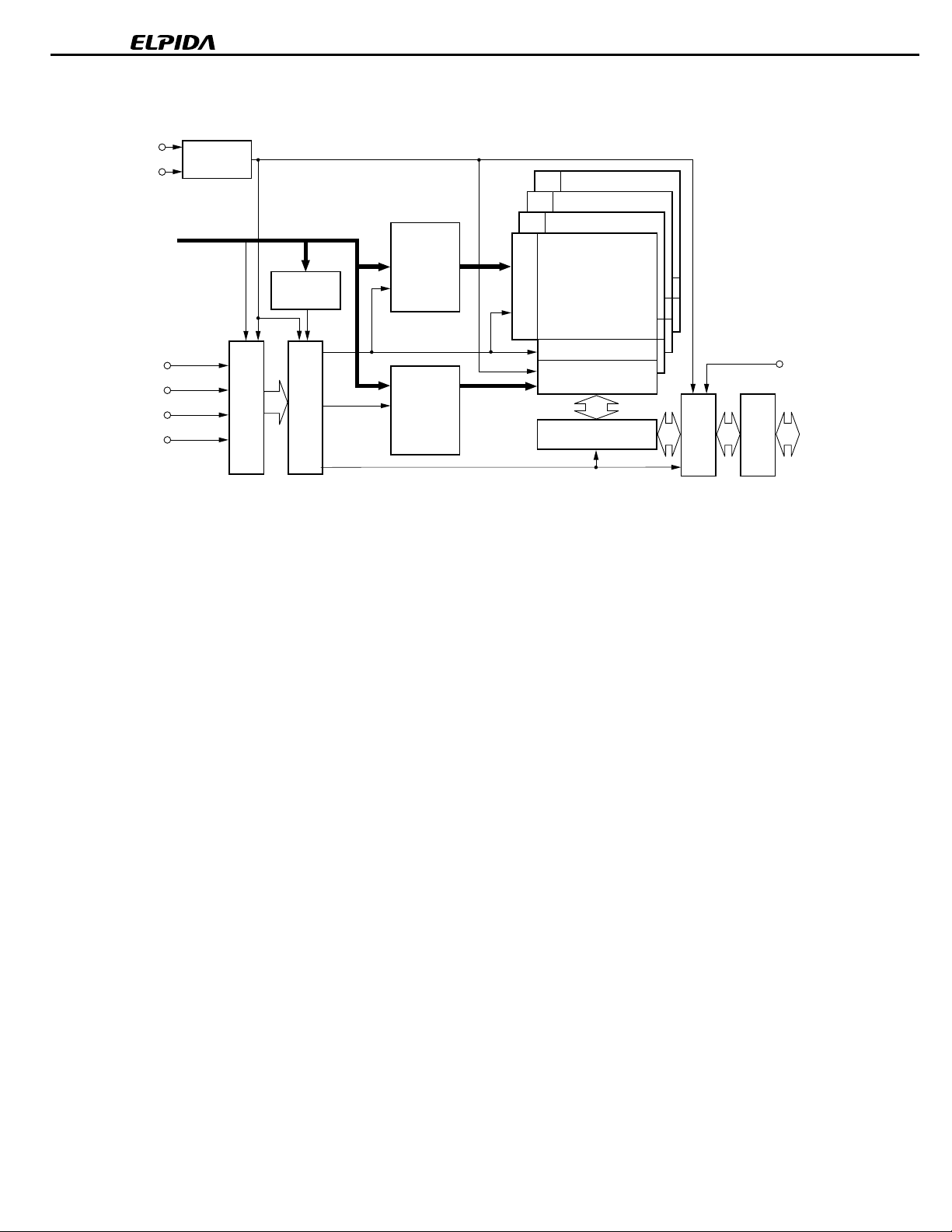
Block Diagram
CLK
CKE
Address
Clock
Generator
Mode
Register
Row
Address
Buffer
&
Refresh
Counter
Bank B
Bank A
Row Decoder
Bank D
Bank C
µµµµ
PD45128163-SU
/CS
/RAS
/CAS
/WE
Control Logic
Command Decoder
Column
Address
Buffer
&
Burst
Counter
Sense Amplifier
Column Decoder &
Latch Circuit
Data Control Circuit
Latch Circuit
DQM
DQ
Input & Output
Buffer
Preliminary Data Sheet E0242N10
5

µµµµ
PD45128163-SU
CONTENTS
1. Input / Output Pin Function .............................................................................................................. 8
2. Commands ......................................................................................................................................... 9
3. Simplified State Diagram ................................................................................................................ 12
4. Truth Table ....................................................................................................................................... 13
4.1 Command Truth Table............................................................................................................................. 13
4.2 DQM Truth Table ...................................................................................................................................... 13
4.3 CKE Truth Table ....................................................................................................................................... 13
4.4 Operative Command Table ..................................................................................................................... 14
4.5 Command Truth Table for CKE .............................................................................................................. 17
5. Initialization ..................................................................................................................................... 18
6. Programming the Mode Register .................................................................................................. 19
7. Mode Register ................................................................................................................................. 20
7.1 Burst Length and Sequence ................................................................................................................... 21
8. Address Bits of Bank-Select and Precharge ................................................................................ 22
9. Precharge ......................................................................................................................................... 23
10. Auto Precharge ................................................................................................................................ 24
10.1 Read with Auto Precharge ................................................................................................................... 24
10.2 Write with Auto Precharge ................................................................................................................... 25
11. Read / Write Command Interval ..................................................................................................... 26
11.1 Read to Read Command Interval ........................................................................................................ 26
11.2 Write to Write Command Interval ........................................................................................................ 26
11.3 Write to Read Command Interval ........................................................................................................ 27
11.4 Read to Write Command Interval ........................................................................................................ 28
12. Burst Termination ........................................................................................................................... 29
12.1 Burst Stop Command ........................................................................................................................... 29
12.2 Precharge Termination ........................................................................................................................ 30
12.2.1 Precharge Termination in READ Cycle .................................................................................... 29
12.2.2 Precharge Termination in WRITE Cycle .................................................................................. 31
6
Preliminary Data Sheet E0242N10

µµµµ
PD45128163-SU
13. Electrical Specifications ................................................................................................................. 32
13.1 AC Parameters for Read Timing .......................................................................................................... 37
13.2 AC Parameters for Write Timing ......................................................................................................... 39
13.3 Relationship between Frequency and Latency .................................................................................. 40
13.4 Mode Register Set ................................................................................................................................ 41
13.5 Power on Sequence and CBR (Auto) Refresh ................................................................................... 42
13.6 /CS Function ......................................................................................................................................... 43
13.7 Clock Suspension during Burst Read (using CKE Function) .......................................................... 44
13.8 Clock Suspension during Burst Write (using CKE Function) .......................................................... 46
13.9 Power Down Mode and Clock Mask ................................................................................................... 48
13.10 CBR (Auto) Refresh .............................................................................................................................. 49
13.11 Self Refresh (Entry and Exit) ............................................................................................................... 50
13.12 Random Column Read (Page with Same Bank) ................................................................................ 51
13.13 Random Column Write (Page with Same Bank) ................................................................................ 53
13.14 Random Row Read (Ping-Pong Banks) .............................................................................................. 55
13.15 Random Row Write (Ping-Pong Banks) ............................................................................................. 57
13.16 Read and Write ..................................................................................................................................... 59
13.17 Interleaved Column Read Cycle .......................................................................................................... 61
13.18 Interleaved Column Write Cycle .......................................................................................................... 63
13.19 Auto Precharge after Read Burst ........................................................................................................ 65
13.20 Auto Precharge after Write Burst ........................................................................................................ 67
13.21 Full Page Read Cycle ........................................................................................................................... 69
13.22 Full Page Write Cycle ........................................................................................................................... 71
13.23 Byte Write Operation ............................................................................................................................ 73
13.24 Burst Read and Single Write (Option) ................................................................................................ 75
13.25 Full Page Random Column Read ........................................................................................................ 77
13.26 Full Page Random Column Write ........................................................................................................ 79
13.27 PRE (Precharge) Termination of Burst ............................................................................................... 81
14. Package Drawing ............................................................................................................................ 83
15. Recommended Soldering Conditions ........................................................................................... 84
16. Revision History .............................................................................................................................. 85
Preliminary Data Sheet E0242N10
7
µµµµ
PD45128163-SU
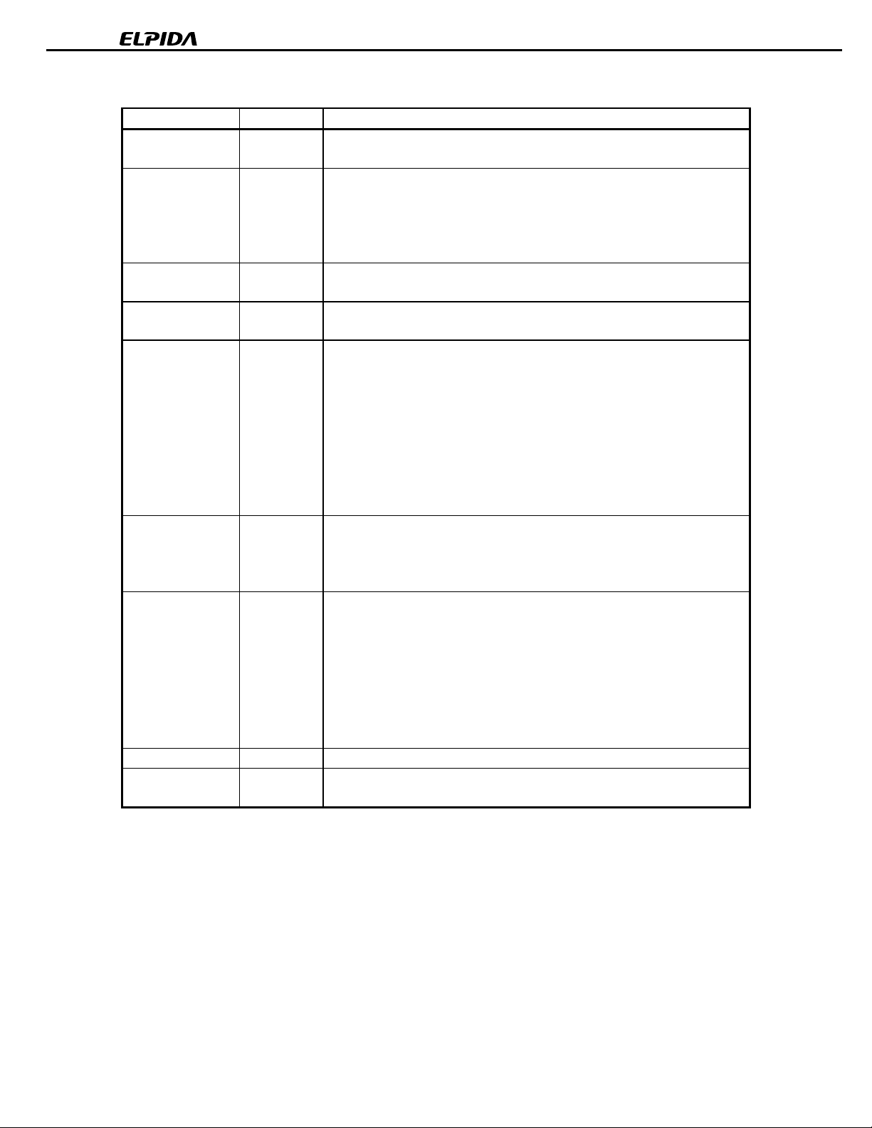
1. Input / Output Pin Function
Pin name Input / Output Function
CLK Input CLK is the master clock input. Other inputs signals are referenced to the CLK rising
edge.
CKE Input CKE determine validity of the next CLK (clock). If CKE is high, the next CLK rising edge
is valid; otherwise it is invalid. If the CLK rising edge is invalid, the internal clock is not
issued and the
When the
power down mode. During power down mode, CKE must remain low.
/CS Input /CS low starts the command input cycle. When /CS is high, commands are ignored but
operations continue.
/RAS, /CAS, /WE Input /RAS, /CAS and /WE have the same symbols on conventional DRAM but different
functions. For details, refer to the command table.
A0 - A11 Input
BA0, BA1 Input BA0(A13) and BA1(A12) are the bank select signal. In command cycle, BA0(A13) and
UDQM, LDQM Input
DQ0 - DQ15 Input / Output DQ pins have the same function as I/O pins on a conventional DRAM.
VCC, VSS, VCCQ, VSSQ (Power supply) VCC and VSS are power supply pins for internal circuits. VCCQ and VSSQ are power
Row Address is determined by A0 - A11 at the CLK (clock) rising edge in the active
command cycle.
Column Address is determined by A0
command cycle.
A10 defines the precharge mode. When A10 is high in the precharge command cycle,
all banks are precharged; when A10 is low, only the bank selected by BA0(A13) and
BA1(A12)
When A10 is high in read or write command cycle, the precharge starts automatically
after the burst access.
BA1(A12) low select bank A, BA0(A13) high and BA1(A12) low select bank B, BA0(A13)
low and BA1(A12) high select bank C and then BA0(A13) and BA1(A12) high select
bank D.
UDQM and LDQM control upper byte and lower byte I/O buffers, respectively.
In read mode, UDQM and LDQM controls the output buffers like a conventional /OE pin.
UDQM and LDQM high and UDQM and LDQM low turn the output buffers off and on,
respectively.
The UDQM and LDQM latency for the read is two clocks.
In write mode, UDQM and LDQM controls the word mask. Input data is written to the
memory cell if UDQM and LDQM is low but not if UDQM and LDQM is high.
The UDQM and LDQM latency for the write is zero.
supply pins for the output buffers.
µ
PD45128163 suspends operation.
µ
PD45128163 is not in burst mode and CKE is negated, the device enters
-
A8 at the CLK rising edge in the read or write
is precharged.
8
Preliminary Data Sheet E0242N10
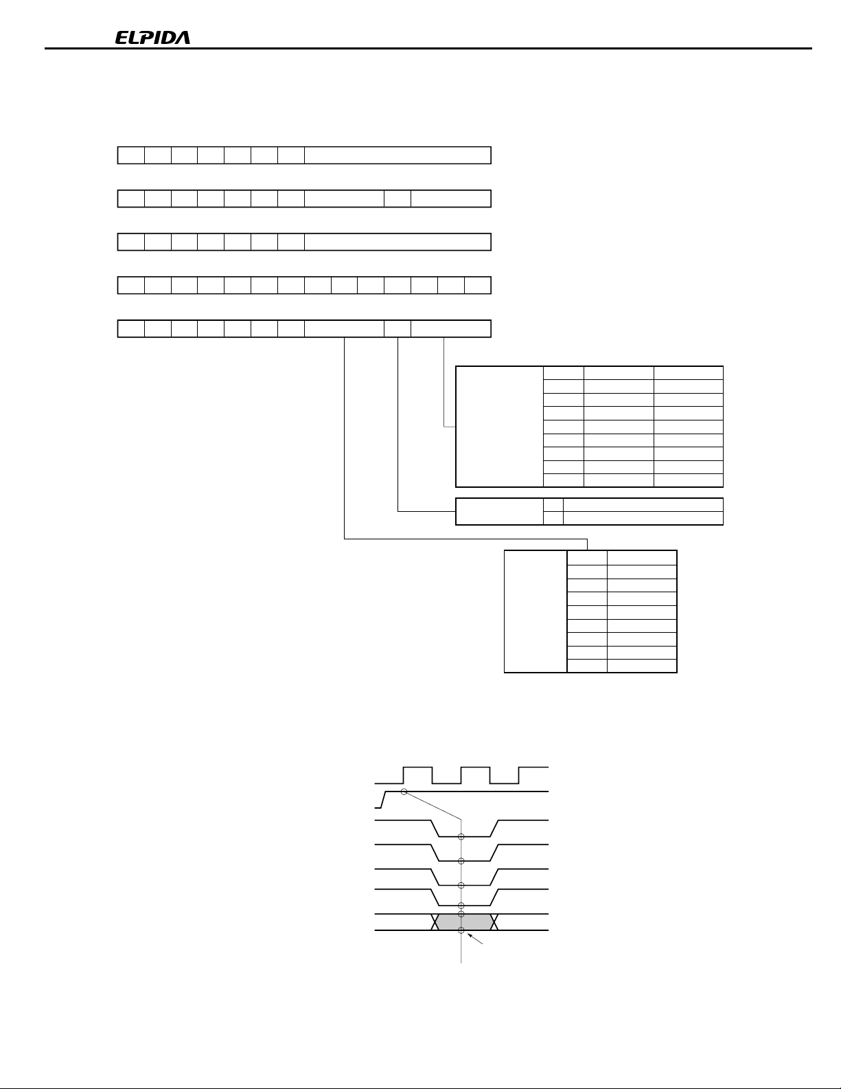
2. Commands
Mode register set command
(/CS, /RAS, /CAS, /WE = Low)
The µPD45128163 has a mode register that defines how the device
operates. In this command, A0 through A11, BA0(A13) and BA1(A12)
are the data input pins. After power on, the mode register set
command must be executed to initialize the device.
The mode register can be set only when all banks are in idle state.
RSC
During 2 CLK (t
cannot accept any other commands.
Activate command
(/CS, /RAS = Low, /CAS, /WE = High)
µ
The
PD45128163 has four banks, each with 4,096 rows.
This command activates the bank selected by BA0(A13) and
BA1(A12) and a row address selected by A0 through A11.
This command corresponds to a conventional DRAM’s /RAS falling.
Precharge command
(/CS, /RAS, /WE = Low, /CAS = High)
This command begins precharge operation of the bank selected by
BA0(A13) and BA1(A12). When A10 is High, all banks are
precharged, regardless of BA0(A13) and BA1(A12). When A10 is
Low, only the bank selected by BA0(A13) and BA1(A12) is
precharged.
After this command, the
command to the precharging bank during t
command period).
This command corresponds to a conventional DRAM’s /RAS rising.
) following this command, the µPD45128163
PD45128163 can’t accept the activate
µ
RP
(precharge to activate
µµµµ
PD45128163-SU
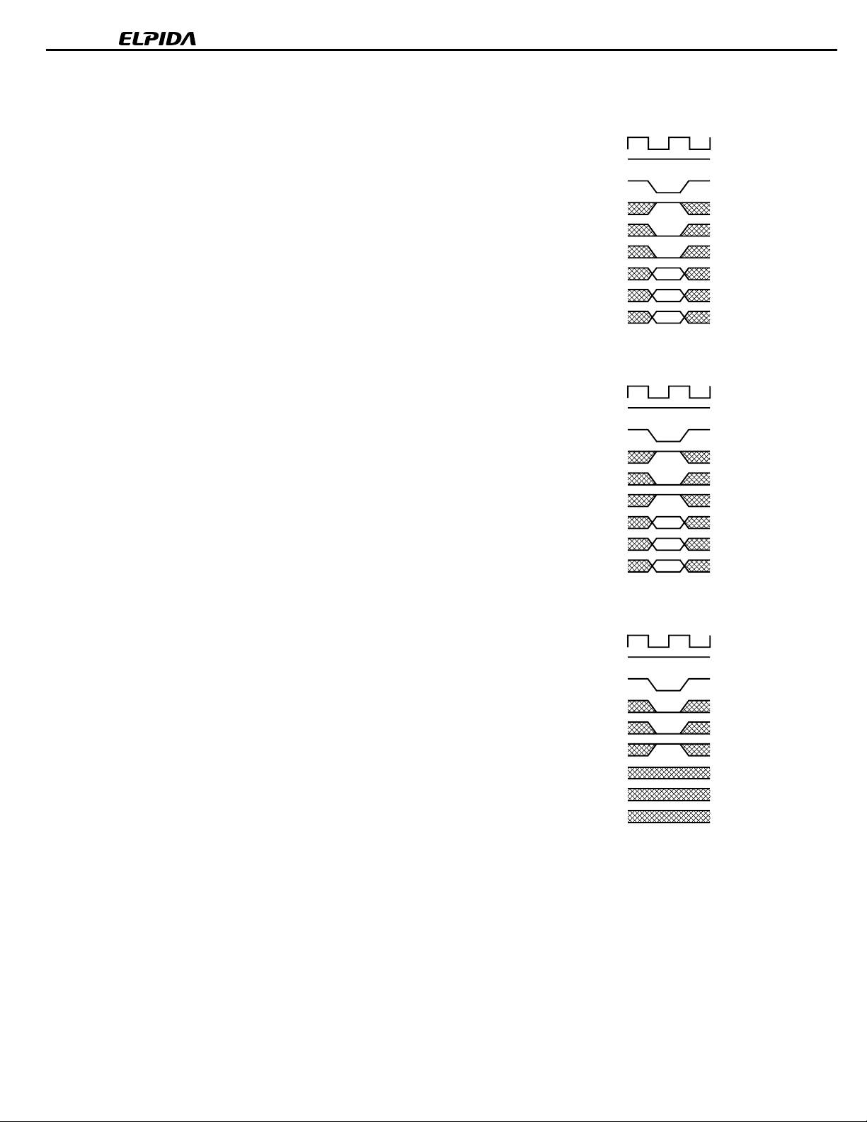
Fig.1 Mode register set command
CLK
CKE
H
/CS
/RAS
/CAS
/WE
BA0(A13), BA1(A12)
A10
Add
Fig.2 Row address strobe and
bank activate command
CLK
CKE
H
/CS
/RAS
/CAS
/WE
BA0(A13), BA1(A12)
A10
Add
Row
Row
Fig.3 Precharge command
CLK
CKE
H
/CS
/RAS
/CAS
/WE
BA0(A13), BA1(A12)
(Precharge select)
A10
Add
Preliminary Data Sheet E0242N10
9
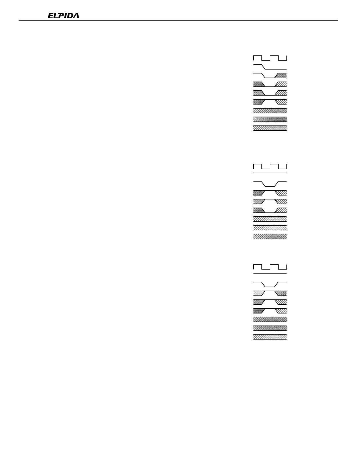
Write command
(/CS, /CAS, /WE = Low, /RAS = High)
If the mode register is in the burst write mode, this command sets the
burst start address given by the column address to begin the burst
write operation. The first write data in burst mode can input with this
command with subsequent data on following clocks.
Read command
(/CS, /CAS = Low, /RAS, /WE = High)
Read data is available after /CAS latency requirements have been
met. This command sets the burst start address given by the column
address.
CBR (auto) refresh command
(/CS, /RAS, /CAS = Low, /WE, CKE = High)
This command is a request to begin the CBR (auto) refresh
operation. The refresh address is generated internally.
Before executing CBR (auto) refresh, all banks must be precharged.
After this cycle, all banks will be in the idle (precharged) state and
ready for a row activate command.
RC
During t
command), the
period (from refresh command to refresh or activate
PD45128163 cannot accept any other command.
µ
µµµµ
PD45128163-SU
Fig.4 Column address and write command
CLK
CKE
H
/CS
/RAS
/CAS
/WE
BA0(A13), BA1(A12)
A10
Add
Col.
Fig.5 Column address and read command
CLK
CKE
H
/CS
/RAS
/CAS
/WE
BA0(A13), BA1(A12)
A10
Add
Col.
Fig.6 CBR (auto) refresh command
CLK
CKE
H
/CS
/RAS
/CAS
/WE
BA0(A13), BA1(A12)
A10
Add
10
Preliminary Data Sheet E0242N10
Self refresh entry command
(/CS, /RAS, /CAS, CKE = Low, /WE = High)
After the command execution, self refresh operation continues while
µ
CKE remains low. When CKE goes high, the
PD45128163 exits the
self refresh mode.
During self refresh mode, refresh interval and refresh operation are
performed internally, so there is no need for external control.
Before executing self refresh, all banks must be precharged.
Burst stop command
(/CS, /WE = Low, /RAS, /CAS = High)
This command can stop the current burst operation.
No operation
(/CS = Low, /RAS, /CAS, /WE = High)
This command is not an execution command. No operations begin
or terminate by this command.
µµµµ
PD45128163-SU
Fig.7 Self refresh entry command
CLK
CKE
/CS
/RAS
/CAS
/WE
BA0(A13), BA1(A12)
A10
Add
Fig.8 Burst stop command in Full Page
Mode
CLK
CKE
H
/CS
/RAS
/CAS
/WE
BA0(A13), BA1(A12)
A10
Add
Fig.9 No operation
CLK
CKE
H
/CS
/RAS
/CAS
/WE
BA0(A13), BA1(A12)
A10
Add
Preliminary Data Sheet E0242N10
11
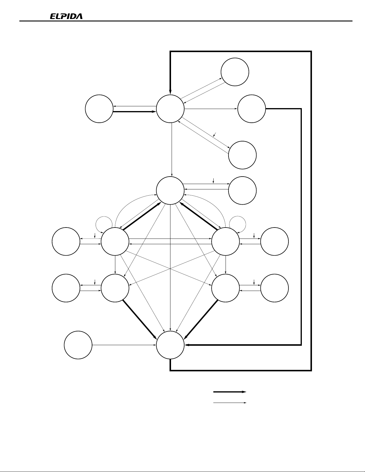
3. Simplified State Diagram
SELF
Self
Refresh
µµµµ
PD45128163-SU
WRITE
SUSPEND
CKE
Mode
Register
Set
Write
CKE
WRITE
BST
MRS
Write
IDLE
ROW
ACTIVE
Write with
Read
Auto precharge
ACT
Auto precharge
PRE
Write
Read
Read with
SELF exit
REF
CKE
CKE
CKE
CKE
BST
READ
CBR (Auto)
Refresh
Power
Down
Active
Power
Down
Read
CKE
CKE
READ
SUSPEND
WRITEA
SUSPEND
12
POWER
ON
CKE
CKE
WRITEA
Precharge
PRE (Precharge termination)
PRE (Precharge termination)
Precharge
Preliminary Data Sheet E0242N10
READA
CKE
CKE
READA
SUSPEND
Automatic sequence
Manual input
µµµµ
PD45128163-SU
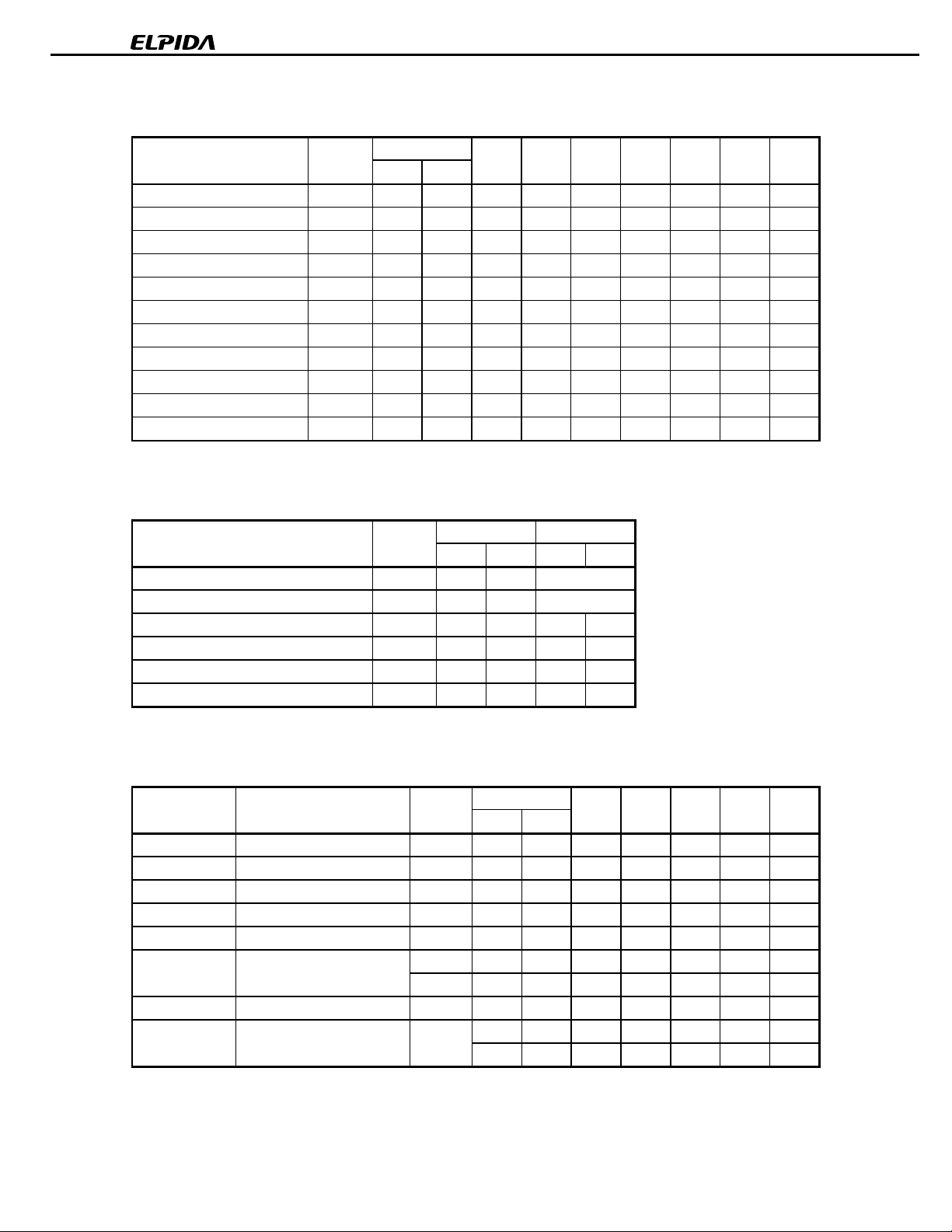
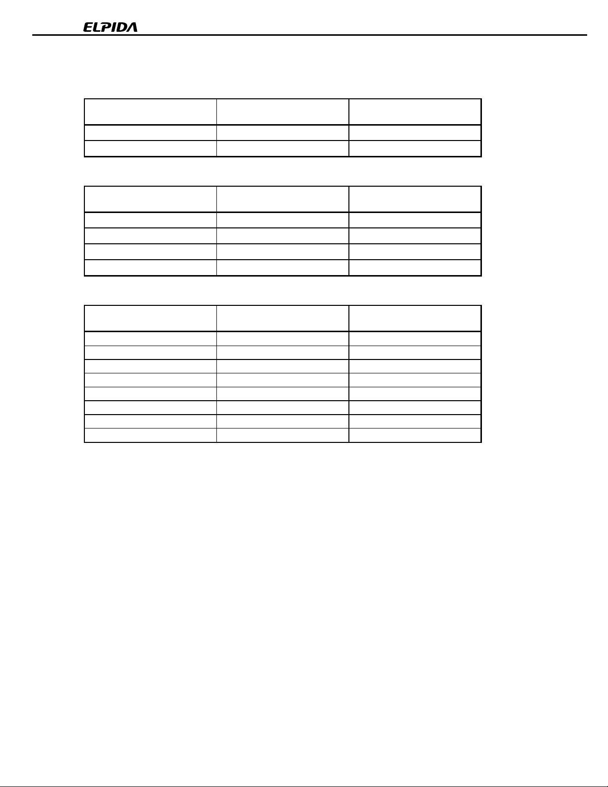
4. Truth Table
4.1 Command Truth Table
Function Symbol CKE /CS /RAS /CAS /WE BA1, A10 A11,
n – 1 n BA0 A9 - A0
Device deselect DESL H × H × × × × × ×
No operation NOP H × L H H H × × ×
Burst stop BST H × L H H L × × ×
Read READ H × L H L H V L V
Read with auto precharge READA H × L H L H V H V
Write WRIT H × L H L L V L V
Write with auto precharge WRITA H × L H L L V H V
Bank activate ACT H × L L H H V V V
Precharge select bank PRE H
Precharge all banks PALL H
Mode register set MRS H
L L H L V L ×
×
L L H L × H ×
×
L L L L L L V
×
Remark
H = High level, L = Low level, × = High or Low level (Don't care), V = Valid data input
4.2 DQM Truth Table
Function Symbol CKE DQM
n – 1 n U L
Data write / output enable ENB H × L
Data mask / output disable MASK H × H
Upper byte write enable / output enable ENBU H × L ×
Lower byte write enable / output enable ENBL H × × L
Upper byte write inhibit / output disable MASKU H × H ×
Lower byte write inhibit / output disable MASKL H × × H
Remark
H = High level, L = Low level, × = High or Low level (Don't care)
4.3 CKE Truth Table
Current state Function Symbol CKE /CS /RAS /CAS /WE Address
n – 1 n
Activating Clock suspend mode entry H L
Any Clock suspend mode L L × × × × ×
Clock suspend Clock suspend mode exit L H × × × × ×
Idle CBR (auto) refresh command REF H H L L L H ×
Idle Self refresh entry SELF H L L L L H ×
Self refresh Self refresh exit L H L H H H ×
L H H × × × ×
Idle Power down entry H L × × × × ×
Power down Power down exit L H H × × × ×
L H L H H H ×
×
×
×
×
×
Remark
H = High level, L = Low level, × = High or Low level (Don't care)
Preliminary Data Sheet E0242N10
13
µµµµ
PD45128163-SU
4.4 Operative Command Table
Current state /CS /RAS /CAS /WE Address Command Action Notes
Idle H × × × × DESL Nop or power down 2
L H H × × NOP or BST Nop or power down 2
L H L H BA, CA, A10 READ/READA ILLEGAL 3
L H L L BA, CA, A10 WRIT/WRITA ILLEGAL 3
L L H H BA, RA ACT Row activating
L L H L BA, A10 PRE/PALL Nop
L L L H × REF/SELF CBR (auto) refresh or self refresh 4
L L L L Op-Code MRS Mode register accessing
Row active H ×
L H H × × NOP or BST Nop
L H L H BA, CA, A10 READ/READA Begin read : Determine AP 5
L H L L BA, CA, A10 WRIT/WRITA Begin write : Determine AP 5
L L H H BA, RA ACT ILLEGAL 3
L L H L BA, A10 PRE/PALL Precharge 6
L L L H × REF/SELF ILLEGAL
L L L L Op-Code MRS ILLEGAL
Read H
L H H H × NOP Continue burst to end → Row active
L H H L
L H L H BA, CA, A10 READ/READA Terminate burst, new read : Determine AP 7
L H L L BA, CA, A10 WRIT/WRITA Terminate burst, start write : Determine AP 7, 8
L L H H BA, RA ACT ILLEGAL 3
L L H L BA, A10 PRE/PALL Terminate burst, precharging
L L L H × REF/SELF ILLEGAL
L L L L Op-Code MRS ILLEGAL
Write H × × × × DESL Continue burst to end → Write recovering
L H H H
L H H L × BST Burst stop → Row active
L H L H BA, CA, A10 READ/READA Terminate burst, start read : Determine AP 7, 8
L H L L BA, CA, A10 WRIT/WRITA Terminate burst, new write : Determine AP 7
L L H H BA, RA ACT ILLEGAL 3
L L H L BA, A10 PRE/PALL Terminate burst, precharging 9
L L L H × REF/SELF ILLEGAL
L L L L Op-Code MRS ILLEGAL
× × × ×
Note1
× × ×
(1/3)
DESL Nop
DESL Continue burst to end → Row active
BST Burst stop
×
NOP Continue burst to end → Write recovering
×
Row active
→
14
Preliminary Data Sheet E0242N10
µµµµ
PD45128163-SU
(2/3)
Current state /CS /RAS /CAS /WE Address Command Action Notes
Read with auto H × × × × DESL Continue burst to end → Precharging
precharge L H H H × NOP Continue burst to end → Precharging
L H H L
L H L H BA, CA, A10 READ/READA ILLEGAL 3
L H L L BA, CA, A10 WRIT/WRITA ILLEGAL 3
L L H H BA, RA ACT ILLEGAL 3
L L H L BA, A10 PRE/PALL ILLEGAL 3
L L L H × REF/SELF ILLEGAL
L L L L Op-Code MRS ILLEGAL
Write with auto
precharge
L H H L × BST ILLEGAL
L H L H BA, CA, A10 READ/READA ILLEGAL 3
L H L L BA, CA, A10 WRIT/WRITA ILLEGAL 3
L L H H BA, RA ACT ILLEGAL 3
L L H L BA, A10 PRE/PALL ILLEGAL 3
L L L H × REF/SELF ILLEGAL
L L L L Op-Code MRS ILLEGAL
Precharging H
L H H H × NOP Nop → Enter idle after t
L H H L
L H L H BA, CA, A10 READ/READA ILLEGAL 3
L H L L BA, CA, A10 WRIT/WRITA ILLEGAL 3
L L H H BA, RA ACT ILLEGAL 3
L L H L BA, A10 PRE/PALL Nop → Enter idle after tRP
L L L H × REF/SELF ILLEGAL
L L L L Op-Code MRS ILLEGAL
Row activating H × × × × DESL Nop → Enter bank active after t
L H H H
L H H L × BST ILLEGAL
L H L H BA, CA, A10 READ/READA ILLEGAL 3
L H L L BA, CA, A10 WRIT/WRITA ILLEGAL 3
L L H H BA, RA ACT ILLEGAL 3, 10
L L H L BA, A10 PRE/PALL ILLEGAL 3
L L L H × REF/SELF ILLEGAL
L L L L Op-Code MRS ILLEGAL
H
×
×
L H H H
× × × ×
BST ILLEGAL
×
×
×
×
DESL Nop
BST ILLEGAL
×
NOP Nop
×
DESL
NOP
Continue burst to end → Write
recovering with auto precharge
Continue burst to end → Write
recovering with auto precharge
Enter idle after tRP
→
RP
RCD
Enter bank active after t
→
RCD
Preliminary Data Sheet E0242N10
15
µµµµ
PD45128163-SU
(3/3)
Current state /CS /RAS /CAS /WE Address Command Action Notes
Write recovering H × × × × DESL Nop → Enter row active after t
L H H H × NOP Nop → Enter row active after t
L H H L
L H L H BA, CA, A10 READ/READA Start read, Determine AP 8
L H L L BA, CA, A10 WRIT/WRITA New write, Determine AP
L L H H BA, RA ACT ILLEGAL 3
L L H L BA, A10 PRE/PALL ILLEGAL 3
L L L H × REF/SELF ILLEGAL
L L L L Op-Code MRS ILLEGAL
Write recovering H × × × × DESL Nop → Enter precharge after t
with auto precharge L H H H × NOP Nop
L H H L × BST Nop → Enter precharge after t
L H L H BA, CA, A10 READ/READA ILLEGAL 3, 8
L H L L BA, CA, A10 WRIT/WRITA ILLEGAL 3
L L H H BA, RA ACT ILLEGAL 3
L L H L BA, A10 PRE/PALL ILLEGAL
L L L H × REF/SELF ILLEGAL
L L L L Op-Code MRS ILLEGAL
Refreshing H
L H H × × NOP/BST Nop → Enter idle after t
L H L
L L H × ×
L L L × ×
Mode register H × × × × DESL Nop → Enter idle after t
accessing L H H H
L H H L × BST ILLEGAL
L H L
× × × ×
L L
×
BST Nop
×
DESL Nop
READ/WRIT ILLEGAL
× ×
ACT/PRE/PALL
REF/SELF/MRS
NOP Nop
×
READ/WRIT ILLEGAL
× ×
×
×
ACT/PRE/PALL/
REF/SELF/MRS
Enter row active after t
→
Enter precharge after t
→
Enter idle after tRC
→
ILLEGAL
ILLEGAL
Enter idle after t
→
ILLEGAL
DPL
DPL
DPL
DPL
DPL
DPL
RC
RSC
RSC
Notes 1.
Remark
16
All entries assume that CKE was active (High level) during the preceding clock cycle.
2.
If all banks are idle, and CKE is inactive (Low level),
µ
PD45128163 will enter Power down mode.
All input buffers except CKE will be disabled.
3.
Illegal to bank in specified states; Function may be legal in the bank indicated by Bank Address (BA),
depending on the state of that bank.
4.
If all banks are idle, and CKE is inactive (Low level),
µ
PD45128163 will enter Self refresh mode. All input
buffers except CKE will be disabled.
5.
Illegal if t
6.
Illegal if t
7.
Must satisfy burst interrupt condition.
8.
Must satisfy bus contention, bus turn around, and/or write recovery requirements.
9.
Must mask preceding data which don't satisfy t
10.
Illegal if t
RCD
is not satisfied.
RAS
is not satisfied.
RRD
is not satisfied.
DPL
.
H = High level, L = Low level, × = High or Low level (Don’t care), V = Valid data
Preliminary Data Sheet E0242N10
µµµµ
PD45128163-SU
4.5 Command Truth Table for CKE
Current State CKE /CS /RAS /CAS /WE Address Action Notes
n – 1 n
Self refresh H × × × × × × INVALID, CLK (n – 1) would exit self refresh
L H H × × × × Self refresh recovery
L H L H H × × Self refresh recovery
L H L H L × × ILLEGAL
L H L L × × × ILLEGAL
L L
Self refresh recovery H H H × × × × Idle after t
H H L H H × × Idle after tRC
H H L H L × × ILLEGAL
H H L L × × × ILLEGAL
H L H
H L L H H × × ILLEGAL
H L L H L × × ILLEGAL
H L L L × × × ILLEGAL
Power down H × × × × × INVALID, CLK (n – 1) would exit power down
L H H
L H L H H H × EXIT power down → Idle
L L × × × × × Maintain power down mode
All banks idle H H H × × × Refer to operations in Operative Command Table
H H L H × × Refer to operations in Operative Command Table
H H L L H × Refer to operations in Operative Command Table
H H L L L H × CBR (auto) Refresh
H H L L L L Op-Code Refer to operations in Operative Command Table
H L H
H L L H × × Refer to operations in Operative Command Table
H L L L H × Refer to operations in Operative Command Table
H L L L L H × Self refresh 1
H L L L L L Op-Code Refer to operations in Operative Command Table
L
Row active H × × × × × × Refer to operations in Operative Command Table
L × × × × × × Power down 1
Any state other than H H × × × × Refer to operations in Operative Command Table
listed above H L × × × × × Begin clock suspend next cycle 2
L H
L L
× × × × ×
× × × ×
× × × ×
× × ×
× × × × × ×
× × × × ×
× × × × ×
Maintain self refresh
RC
ILLEGAL
EXIT power down → Idle
Refer to operations in Operative Command Table
Power down 1
Exit clock suspend next cycle
Maintain clock suspend
Notes 1.
Self refresh can be entered only from the all banks idle state. Power down can be entered only from all
banks idle or row active state.
2.
Must be legal command as defined in Operative Command Table.
Remark
H = High level, L = Low level, × = High or Low level (Don't care)
Preliminary Data Sheet E0242N10
17

µµµµ
PD45128163-SU
5. Initialization
The synchronous DRAM is initialized in the power-on sequence according to the following.
µ
(1) To stabilize internal circuits, when power is applied, a 100
(2) After the pause, all banks must be precharged using the Precharge command (The Precharge all banks
command is convenient).
(3) Once the precharge is completed and the minimum t
RSC
After the mode register set cycle, t
(4) Two or more CBR (Auto) refresh must be performed.
Remarks 1.
The sequence of Mode register programming and Refresh above may be transposed.
2.
CKE and DQM must be held high until the Precharge command is issued to ensure data-bus Hi-Z.
(2 CLK minimum) pause must be satisfied as well.
s or longer pause must precede any signal toggling.
RP
is satisfied, the mode register can be programmed.
18
Preliminary Data Sheet E0242N10

µµµµ
PD45128163-SU
6. Programming the Mode Register
The mode register is programmed by the Mode register set command using address bits A11 through A0, BA0(A13)
and BA1(A12) as data inputs. The register retains data until it is reprogrammed or the device loses power.
The mode register has four fields;
Options : A11 through A7, BA0(A13), BA1(A12)
/CAS latency : A6 through A4
Wrap type : A3
Burst length : A2 through A0
Following mode register programming, no command can be issued before at least 2 CLK have elapsed.
/CAS Latency
/CAS latency is the most critical of the parameters being set. It tells the device how many clocks must elapse
before the data will be available.
The value is determined by the frequency of the clock and the speed grade of the device.
between Frequency and Latency
the device.
Burst Length
Burst Length is the number of words that will be output or input in a read or write cycle. After a read burst is
completed, the output bus will become Hi-Z.
The burst length is programmable as 1, 2, 4, 8 or full page.
Wrap Type (Burst Sequence)
The wrap type specifies the order in which the burst data will be addressed. This order is programmable as either
“Sequential” or “Interleave”. The method chosen will depend on the type of CPU in the system.
Some microprocessor cache systems are optimized for sequential addressing and others for interleaved addressing.
7.1 Burst Length and Sequence
sequences support bursts of 1, 2, 4 and 8. Additionally, sequence supports the full page length.
shows the relationship of /CAS latency to the clock period and the speed grade of
shows the addressing sequence for each burst length using them. Both
13.3 Relationship
Preliminary Data Sheet E0242N10
19
7. Mode Register
BA1
BA0
(A12)
(A13)
00
BA1
BA0
(A12)
(A13)
xx
BA1
BA0
(A12)
(A13)
BA1
BA0
(A12)
(A13)
xx
BA1
BA0
(A12)
(A13)
00
µµµµ
PD45128163-SU
A0A1A2A3A4A5A7 A6A8A9A10A11
10000 JEDEC Standard Test Set (refresh counter test)
A0A1A2A3A4A5A7 A6A8A9A10A11
BLWTLTMODE001xx Burst Read and Single Write
01 Use in future
BLWTLTMODE00000 Mode Register Set
(for Write Through Cache)
A0A1A2A3A4A5A7 A6A8A9A10A11
A0A1A2A3A4A5A7 A6A8A9A10A11
VVVVVV1V1xxx Vender Specific
A0A1A2A3A4A5A7 A6A8A9A10A11
V = Valid
x = Don’t care
Burst length
Wrap type
Latency
Remark R : Reserved
Mode Register Set Timing
mode
Bits2-0
000
001
010
011
100
101
110
111
0
1
Full page
Sequential
Interleave
Bits6-4
000
001
010
011
100
101
110
111
WT = 0
1
2
4
8
R
R
R
/CAS latency
WT = 1
1
2
4
8
R
R
R
R
R
R
2
3
R
R
R
R
20
CLK
CKE
/CS
/RAS
/CAS
/WE
A0 - A11,
BA0(13), BA1(A12)
Preliminary Data Sheet E0242N10
Mode Register Set
7.1 Burst Length and Sequence
[Burst of Two]
Starting address
(column address A0, binary)
0 0, 1 0, 1
1 1, 0 1, 0
[Burst of Four]
Starting address
(column address A1 - A0, binary)
00 0, 1, 2, 3 0, 1, 2, 3
01 1, 2, 3, 0 1, 0, 3, 2
10 2, 3, 0, 1 2, 3, 0, 1
11 3, 0, 1, 2 3, 2, 1, 0
[Burst of Eight]
Starting address
(column address A2 - A0, binary)
000 0, 1, 2, 3, 4, 5, 6, 7 0, 1, 2, 3, 4, 5, 6, 7
001 1, 2, 3, 4, 5, 6, 7, 0 1, 0, 3, 2, 5, 4, 7, 6
010 2, 3, 4, 5, 6, 7, 0, 1 2, 3, 0, 1, 6, 7, 4, 5
011 3, 4, 5, 6, 7, 0, 1, 2 3, 2, 1, 0, 7, 6, 5, 4
100 4, 5, 6, 7, 0, 1, 2, 3 4, 5, 6, 7, 0, 1, 2, 3
101 5, 6, 7, 0, 1, 2, 3, 4 5, 4, 7, 6, 1, 0, 3, 2
110 6, 7, 0, 1, 2, 3, 4, 5 6, 7, 4, 5, 2, 3, 0, 1
111 7, 0, 1, 2, 3, 4, 5, 6 7, 6, 5, 4, 3, 2, 1, 0
Sequential addressing sequence
(decimal)
Sequential addressing sequence
(decimal)
Sequential addressing sequence
(decimal)
µµµµ
PD45128163-SU
Interleave addressing sequence
(decimal)
Interleave addressing sequence
(decimal)
Interleave addressing sequence
(decimal)
Full page burst is an extension of the above tables of sequential addressing, with the length being 512.
Preliminary Data Sheet E0242N10
21

8. Address Bits of Bank-Select and Precharge
(Activate command)
(Precharge command)
(/CAS strobes)
µµµµ
PD45128163-SU
BA1
(A12)
BA1
(A12)
BA1
(A12)
BA0
(A13)
BA0
(A13)
BA0
(A13)
A11A10A9A8A7A6A4 A5A3A2A1A0Row
A11A10A9A8A7A6A4 A5A3A2A1A0
xA10A9A8A7A6A4 A5A3A2A1A0Col.
BA1(A12) BA0(A13)
0
0
0
1
1
0
1
1
BA1(A12) BA0(A13)
A10
0
0
0
0
0
1
0
1
1
x
x : Don’t care
disables Auto-Precharge
0
(End of Burst)
enables Auto-Precharge
1
(End of Burst)
Result
Select Bank A
“Activate” command
Select Bank B
“Activate” command
Select Bank C
“Activate” command
Select Bank D
“Activate” command
Result
Precharge Bank A
0
Precharge Bank B
1
Precharge Bank C
0
Precharge Bank D
1
Precharge All Banks
x
BA1(A12) BA0(A13)
0
0
0
1
1
0
1
1
Result
enables Read/Write
commands for Bank A
enables Read/Write
commands for Bank B
enables Read/Write
commands for Bank C
enables Read/Write
commands for Bank D
22
Preliminary Data Sheet E0242N10
µµµµ
PD45128163-SU
9. Precharge
RAS (MIN.)
The precharge command can be issued anytime after t
Soon after the precharge command is issued, precharge operation performed and the synchronous DRAM enters
RP
the idle state after t
is satisfied. The parameter tRP is the time required to perform the precharge.
The earliest timing in a read cycle that a precharge command can be issued without losing any data in the burst is
as follows.
It is depending on the /CAS latency and clock cycle time.
T0 T1 T2 T3 T4 T5 T6 T7
CLK
/CAS latency = 2
Command
READ
is satisfied.
Burst length=4
T8
PRE
Hi-Z
Hi-Z
/CAS latency = 3
Command
DQ
DQ
READ
Q1 Q2 Q3 Q4
PRE
Q1 Q2 Q3 Q4
(t
RAS
must be satisfied)
DPL
In order to write all data to the memory cell correctly, the asynchronous parameter “t
(MIN.)
specification defines the earliest time that a precharge command can be issued. Minimum number of clocks is
DPL (MIN.)
calculated by dividing t
with clock cycle time.
” must be satisfied. The t
In summary, the precharge command can be issued relative to reference clock that indicates the last data word is
valid. In the following table, minus means clocks before the reference; plus means time after the reference.
/CAS latency Read Write
2 –1 +t
3 –2 +t
DPL (MIN.)
DPL (MIN.)
DPL
Preliminary Data Sheet E0242N10
23
µµµµ
PD45128163-SU
10. Auto Precharge
During a read or write command cycle, A10 controls whether auto precharge is selected. A10 high in the Read or
Write command (Read with Auto precharge command or Write with Auto precharge command), auto precharge is
selected and begins automatically.
RAS
The t
next activate command to the bank being precharged cannot be executed until the precharge cycle ends.
In read cycle, once auto precharge has started, an activate command to the bank can be issued after t
satisfied.
In write cycle, the t
The timing that begins the auto precharge cycle depends on both the /CAS latency programmed into the mode
register and whether read or write cycle.
10.1 Read with Auto Precharge
During a read cycle, the auto precharge begins one clock earlier (/CAS latency of 2) or two clocks earlier (/CAS
latency of 3) the last data word output.
must be satisfied with a read with auto precharge or a write with auto precharge operation. In addition, the
RP
has been
DAL
must be satisfied to issue the next activate command to the bank being precharged.
Burst length = 4
T0 T2T1 T3 T4 T5 T6 T7 T8
CLK
T9
/CAS latency = 2
Command
DQ
/CAS latency = 3
Command
DQ
Remark
READA means Read with Auto precharge
READA B
READA B
Auto precharge starts
QB1 QB2 QB3 QB4
Auto precharge starts
QB1 QB2 QB3 QB4
Hi-Z
(t
RAS
must be satisfied)
Hi-Z
24
Preliminary Data Sheet E0242N10
10.2 Write with Auto Precharge
During a write cycle, the auto precharge starts at the timing that is equal to the value of the t
data word input to the device.
T0 T2T1 T3 T4 T5 T6 T7 T8
CLK
µµµµ
PD45128163-SU
DPL (MIN.)
after the last
Burst length = 4
/CAS latency = 2
Command
DQ
/CAS latency = 3
Command
DQ
WRITA B
DB1 DB2 DB3 DB4
WRITA B
DB1 DB2 DB3 DB4
Auto precharge starts
t
DPL(MIN.)
Auto precharge starts
t
DPL(MIN.)
Hi-Z
Hi-Z
RAS
must be satisfied)
(t
Remark
WRITA means Write with Auto Precharge
In summary, the auto precharge begins relative to a reference clock that indicates the last data word is valid.
In the table below, minus means clocks before the reference; plus means after the reference.
/CAS latency Read Write
2 –1 +t
3 –2 +t
DPL (MIN.)
DPL (MIN.)
Preliminary Data Sheet E0242N10
25
µµµµ
PD45128163-SU
11. Read / Write Command Interval
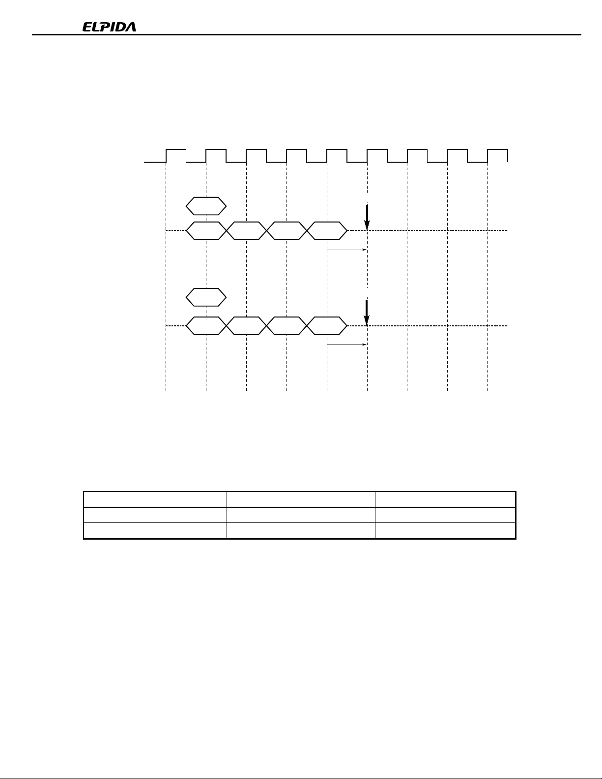
11.1 Read to Read Command Interval
During a read cycle, when new Read command is issued, it will be effective after /CAS latency, even if the previous
read operation does not completed. READ will be interrupted by another READ.
The interval between the commands is 1 cycle minimum. Each Read command can be issued in every clock
without any restriction.
T0 T2T1 T3 T4 T5 T6 T7 T8
CLK
Burst length = 4, /CAS latency = 2
T9
Command
DQ
READ A
1cycle
READ B
QA1
QB1 QB2 QB3 QB4
Hi-Z
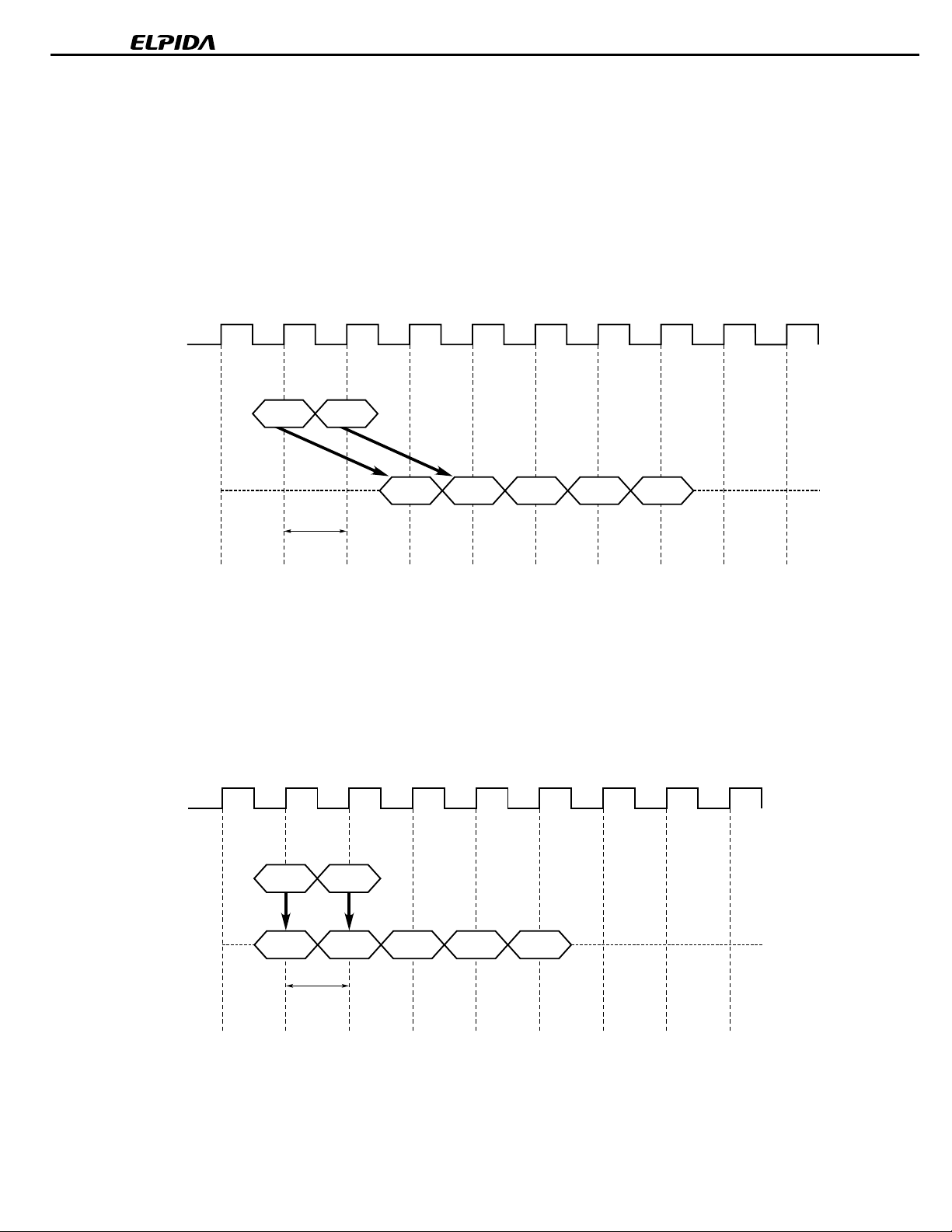
11.2 Write to Write Command Interval
During a write cycle, when a new Write command is issued, the previous burst will terminate and the new burst will
begin with a new Write command. WRITE will be interrupted by another WRITE.
The interval between the commands is minimum 1 cycle. Each Write command can be issued in every clock
without any restriction.
Burst length = 4, /CAS latency = 2
T0 T2T1 T3 T4 T5 T6 T7 T8
CLK
Command
DQ
26
WRITE A
DA1
WRITE B
DB1 DB2 DB3 DB4
1cycle
Preliminary Data Sheet E0242N10
Hi-Z
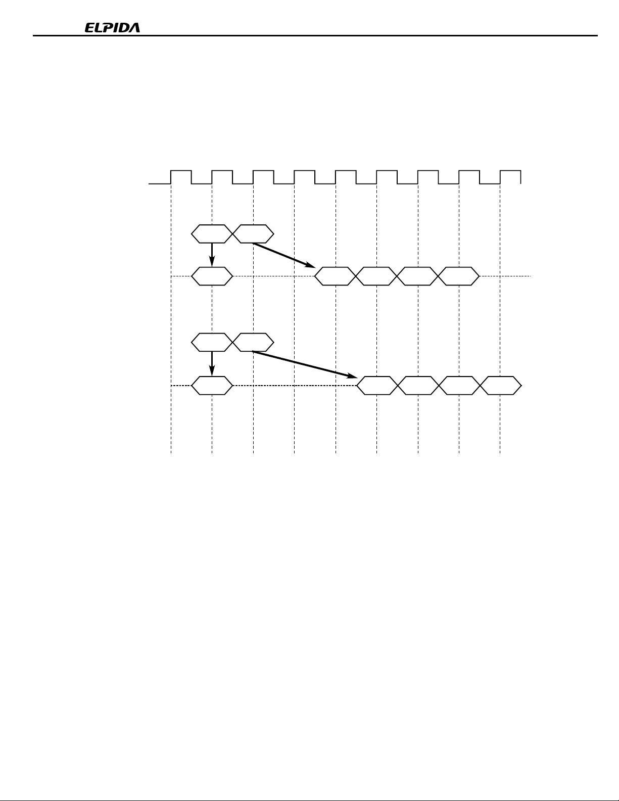
11.3 Write to Read Command Interval
Write command and Read command interval is also 1 cycle.
Only the write data before Read command will be written.
The data bus must be Hi-Z at least one cycle prior to the first D
T0 T2T1 T3 T4 T5 T6 T7 T8
CLK
/CAS latency = 2
Command
WRITE A
READ B
OUT
µµµµ
PD45128163-SU
.
Burst length = 4
DQ
/CAS latency = 3
Command
DQ
DA1
WRITE A
DA1
READ B
Hi-Z
Hi-Z
QB1 QB2 QB3 QB4
QB1 QB2 QB3 QB4
Preliminary Data Sheet E0242N10
27
 Loading...