

ELPIDA MC-4R128FKE8S-840 Datasheet

DATA SHEET
MOS INTEGRATED CIRCUIT
MC-4R128FKE8S-840
Direct Rambus DRAM SO-RIMMTM Module
128M-BYTE (64M-WORD x 18-BIT)
Description
The Direct Rambus SO-RIMM module is a general-purpose high-performance memory module subsystem suitable
for use in a broad range of applications including computer memory, mobile personal computers, networking
systems, and other applications where high bandwidth and low latency are required.
MC-4R128FKE8S modules consists of four 288M Direct Rambus DRAM (Direct RDRAM) devices (
These are extremely high-speed CMOS DRAMs organized as 16M words by 18 bits. The use of Rambus Signaling
Level (RSL) technology permits 800MHz transfer rates while using conventional system and board design
technologies.
Direct RDRAM devices are capable of sustained data transfers at 1.25 ns per two bytes (10 ns per 16 bytes).
The architecture of the Direct RDRAM enables the highest sustained bandwidth for multiple, simultaneous,
randomly addressed memory transactions. The separate control and data buses with independent row and column
control yield high bus efficiency. The Direct RDRAM's multi-bank architecture supports up to four simultaneous
transactions per device.
Features
PD488588).
µ
• 160 edge connector pads with 0.65mm pad spacing
• 128 MB Direct RDRAM storage
• Each RDRAM
• Gold plated contacts
• RDRAMs use Chip Scale Package (CSP)
• Serial Presence Detect support
• Operates from a 2.5 V supply
• Powerdown self refresh modes
• Separate Row and Column buses for higher efficiency
Document No. E0258N20 (Ver. 2.0)
Date Published June 2002 (K) Japan
URL: http://www.elpida.com
has 32 banks, for 128 banks total on module
The information in this document is subject to change without notice. Before using this document, please
confirm that this is the latest version.
Not all devices/types available in every country. Please check with local Elpida Memory, Inc. for
availability and additional information.
Elpida Memory, Inc. is a joint venture DRAM company of NEC Corporation and Hitachi, Ltd.
Elpida Memory,Inc. 2002

Order information
MC-4R128FKE8S-840
Part number Organization I/O Freq.
MHz
MC-4R128FKE8S - 840 64M x 18 800 40
RAS access time
ns
Package Mounted devices
160 edge connector pads
SO-RIMM with heat spreader
Edge connector: Gold plated
4 pieces of µPD488588FF
BGA) package
µ
FBGA (
2
Data Sheet E0258N20 (Ver. 2.0)
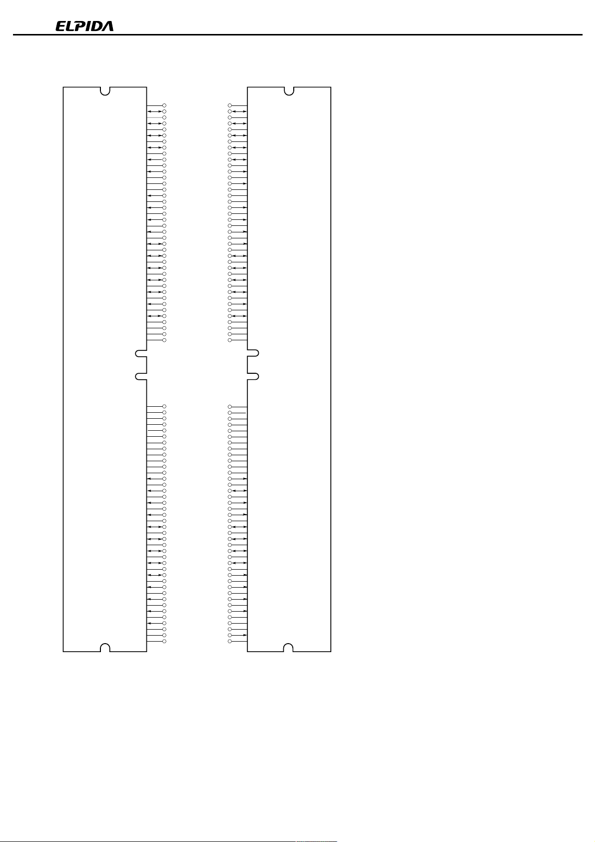
Module Pad Configuration
MC-4R128FKE8S-840
GND
LDQA8
GND
LDQA6
GND
LDQA4
GND
LDQA2
GND
LDQA0
GND
LCTM
GND
LCTMN
GND
LROW1
GND
LCOL4
GND
LCOL2
GND
LCOL0
GND
LDQB0
GND
LDQB2
GND
LDQB4
GND
LDQB6
GND
LSCK
GND
SOUT
V
NC
GND
NC
V
CMOS
NC
A1
A2
A3
A4
A5
A6
A7
A8
A9
A10
A11
A12
A13
A14
A15
A16
A17
A18
A19
A20
A21
A22
A23
A24
A25
A26
A27
A28
A29
A30
A31
A32
A33
DD
A34
A35
A36
A37
A38
A39
A40
B10
B11
B12
B13
B14
B15
B16
B17
B18
B19
B20
B21
B22
B23
B24
B25
B26
B27
B28
B29
B30
B31
B32
B33
B34
B35
B36
B37
B38
B39
B40
B1
B2
B3
B4
B5
B6
B7
B8
B9
GND
LDQA7
GND
LDQA5
GND
LDQA3
GND
LDQA1
GND
LCFM
GND
LCFMN
GND
LROW2
GND
LROW0
GND
LCOL3
GND
LCOL1
GND
LDQB1
GND
LDQB3
GND
LDQB5
GND
LDQB7
GND
LDQB8
GND
LCMD
GND
SIN
V
DD
NC
GND
NC
V
CMOS
NC
Side B Side A
B41
B42
B43
B44
B45
B46
B47
B48
B49
B50
B51
B52
B53
B54
B55
B56
B57
B58
B59
B60
B61
B62
B63
B64
B65
B66
B67
B68
B69
B70
B71
B72
B73
B74
B75
B76
B77
B78
B79
B80
NC
REF
V
SA0
DD
V
SA1
DD
V
SWP
GND
RCMD
GND
RDQB6
GND
RDQB4
GND
RDQB2
GND
RDQB0
GND
RCOL0
GND
RCOL2
GND
RCOL4
GND
RROW1
GND
RCTMN
GND
RCTM
GND
RDQA0
GND
RDQA2
GND
RDQA4
GND
RDQA6
GND
RDQA8
GND
NC
V
REF
SCL
V
SDA
V
SV
GND
RSCK
GND
RDQB8
GND
RDQB7
GND
RDQB5
GND
RDQB3
GND
RDQB1
GND
RCOL1
GND
RCOL3
GND
RROW0
GND
RROW2
GND
RCFMN
GND
RCFM
GND
RDQA1
GND
RDQA3
GND
RDQA5
GND
RDQA7
GND
A41
A42
DD
DD
DD
A43
A44
A45
A46
A47
A48
A49
A50
A51
A52
A53
A54
A55
A56
A57
A58
A59
A60
A61
A62
A63
A64
A65
A66
A67
A68
A69
A70
A71
A72
A73
A74
A75
A76
A77
A78
A79
A80
LCFM, LCFMN,
RCFM, RCFMN : Clock from master
LCTM, LCTMN,
RCTM, RCTMN : Clock to master
LCMD, RCMD : Serial Command Pad
LROW2 - LROW0,
RROW2 - RROW0 : Row bus
LCOL4 - LCOL0,
RCOL4 - RCOL0 : Column bus
LDQA8 - LDQA0,
RDQA8 - RDQA0 : Data bus A
LDQB8 - LDQB0,
RDQB8 - RDQB0 : Data bus B
LSCK, RSCK : Clock input
SA0, SA1 : Serial Presence Detect Address
SCL, SDA : Serial Presence Detect Clock
SIN, SOUT : Serial I/O
SVDD : SPD Voltage
SWP : Serial Presence Detect Write Protect
V
: Supply voltage for serial pads
CMOS
VDD : Supply voltage
V
: Logic threshold
REF
GND : Ground reference
NC : These pads are not connected
Data Sheet E0258N20 (Ver. 2.0)
3
MC-4R128FKE8S-840
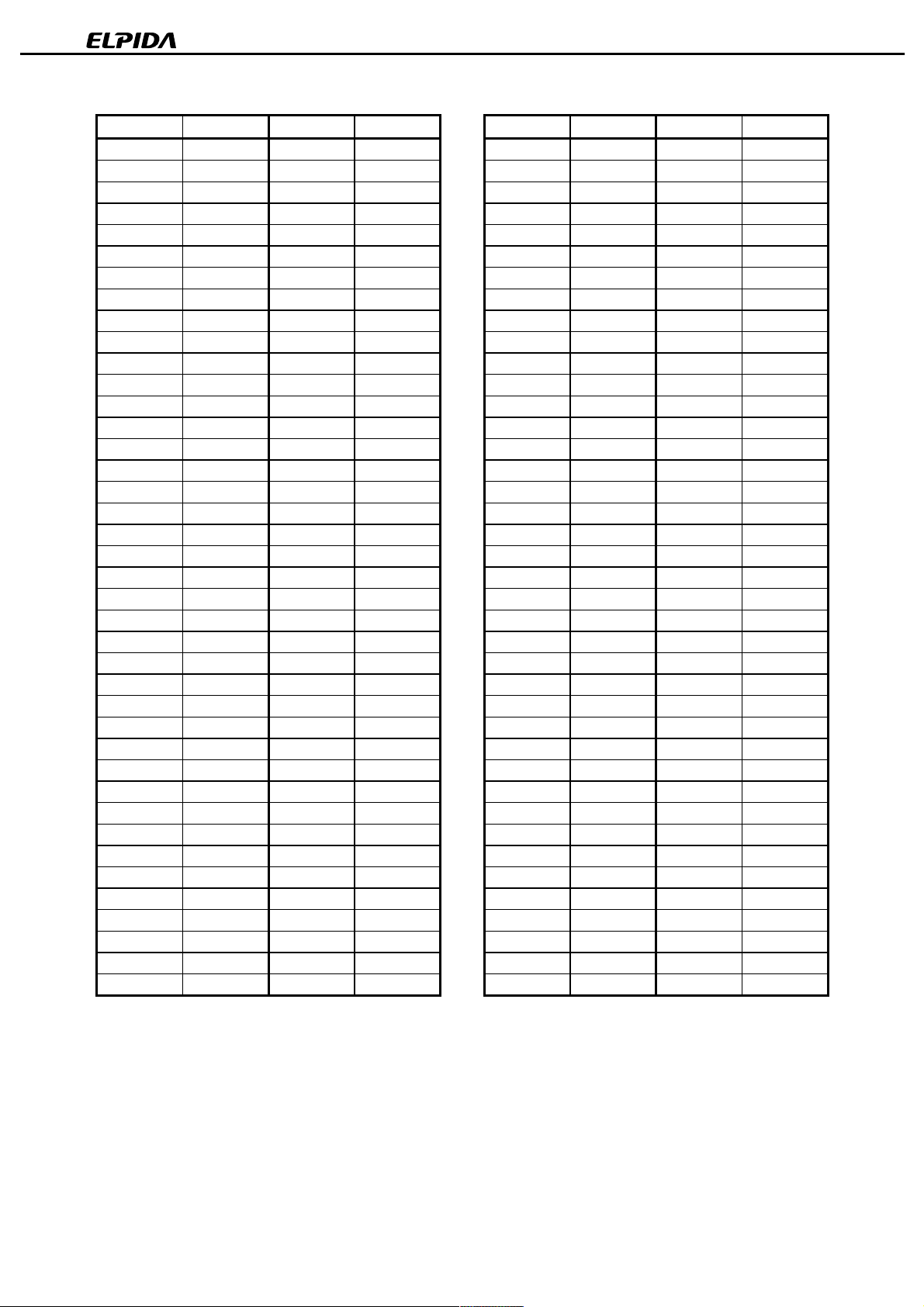
Module Pad Names
Pad Signal Name Pad Signal Name Pad Signal Name Pad Signal Name
A1 GND B1 GND A41 NC B41 NC
A2 LDQA8 B2 LDQA7 A42 V
A3 GND B3 GND A43 SCL B43 SA0
A4 LDQA6 B4 LDQA5 A44 VDD B44 VDD
A5 GND B5 GND A45 SDA B45 SA1
A6 LDQA4 B6 LDQA3 A46 VDD B46 VDD
A7 GND B7 GND A47 SVDD B47 SWP
A8 LDQA2 B8 LDQA1 A48 GND B48 GND
A9 GND B9 GND A49 RSCK B49 RCMD
A10 LDQA0 B10 LCFM A50 GND B50 GND
A11 GND B11 GND A51 RDQB8 B51 RDQB6
A12 LCTM B12 LCFMN A52 GND B52 GND
A13 GND B13 GND A53 RDQB7 B53 RDQB4
A14 LCTMN B14 LROW2 A54 GND B54 GND
A15 GND B15 GND A55 RDQB5 B55 RDQB2
A16 LROW1 B16 LROW0 A56 GND B56 GND
A17 GND B17 GND A57 RDQB3 B57 RDQB0
A18 LCOL4 B18 LCOL3 A58 GND B58 GND
A19 GND B19 GND A59 RDQB1 B59 RCOL0
A20 LCOL2 B20 LCOL1 A60 GND B60 GND
A21 GND B21 GND A61 RCOL1 B61 RCOL2
A22 LCOL0 B22 LDQB1 A62 GND B62 GND
A23 GND B23 GND A63 RCOL3 B63 RCOL4
A24 LDQB0 B24 LDQB3 A64 GND B64 GND
A25 GND B25 GND A65 RROW0 B65 RROW1
A26 LDQB2 B26 LDQB5 A66 GND B66 GND
A27 GND B27 GND A67 RROW2 B67 RCTMN
A28 LDQB4 B28 LDQB7 A68 GND B68 GND
A29 GND B29 GND A69 RCFMN B69 RCTM
A30 LDQB6 B30 LDQB8 A70 GND B70 GND
A31 GND B31 GND A71 RCFM B71 RDQA0
A32 LSCK B32 LCMD A72 GND B72 GND
A33 GND B33 GND A73 RDQA1 B73 RDQA2
A34 SOUT B34 SIN A74 GND B74 GND
A35 VDD B35 VDD A75 RDQA3 B75 RDQA4
A36 NC B36 NC A76 GND B76 GND
A37 GND B37 GND A77 RDQA5 B77 RDQA6
A38 NC B38 NC A78 GND B78 GND
A39 V
CMOS
B39 V
CMOS
A79 RDQA7 B79 RDQA8
A40 NC B40 NC A80 GND B80 GND
REF
B42 V
REF
4
Data Sheet E0258N20 (Ver. 2.0)
MC-4R128FKE8S-840
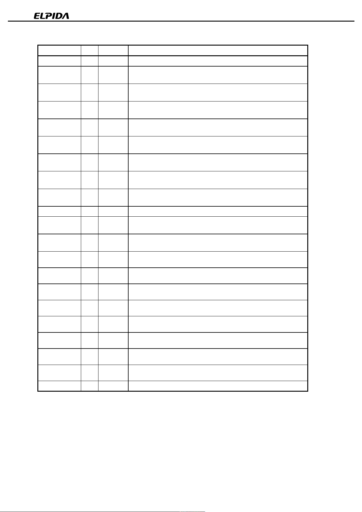
Module Connector Pad Description (1/2)
Signal I/O Type Description
GND – – Ground reference for RDRAM core and interface.
LCFM I RSL Clock from master. Interface clock used for receiving RSL signals from the
Channel. Positive polarity.
LCFMN I RSL Clock from master. Interface clock used for receiving RSL signals from the
Channel. Negative polarity.
LCMD I V
LCOL4..LCOL0 I RSL Column bus. 5-bit bus containing control and address information for column
LCTM I RSL Clock to master. Interface clock used for transmitting RSL signals to the
LCTMN I RSL Clock to master. Interface clock used for transmitting RSL signals to the
LDQA8..LDQA0 I/O RSL Data bus A. A 9-bit bus carrying a byte of read or write data between the Channel
LDQB8..LDQB0 I/O RSL Data bus B. A 9-bit bus carrying a byte of read or write data between the Channel
LROW2..LROW0 I RSL Row bus. 3-bit bus containing control and address information for row accesses.
LSCK I V
NC – – These pads are not connected. These 8 connector pads are reserved for future
RCFM I RSL Clock from master. Interface clock used for receiving RSL signals from the
RCFMN I RSL Clock from master. Interface clock used for receiving RSL signals from the
RCMD I V
RCOL4..RCOL0 I RSL Column bus. 5-bit bus containing control and address information for column
RCTM I RSL Clock to master. Interface clock used for transmitting RSL signals to the
RCTMN I RSL Clock to master. Interface clock used for transmitting RSL signals to the
RDQA8..RDQA0 I/O RSL Data bus A. A 9-bit bus carrying a byte of read or write data between the Channel
RDQB8..RDQB0 I/O RSL Data bus B. A 9-bit bus carrying a byte of read or write data between the Channel
RROW2..RROW0 I RSL Row bus. 3-bit bus containing control and address information for row accesses.
Serial Command used to read from and write to the control registers. Also used
CMOS
for power management.
accesses.
Channel. Positive polarity.
Channel. Negative polarity.
and the RDRAM. LDQA8 is non-functional on modules with x16 RDRAM devices.
and the RDRAM. LDQB8 is non-functional on modules with x16 RDRAM devices.
Serial clock input. Clock source used to read from and write to the RDRAM
CMOS
control registers.
use.
Channel. Positive polarity.
Channel. Negative polarity.
Serial Command Input used to read from and write to the control registers. Also
CMOS
used for power management.
accesses.
Channel. Positive polarity.
Channel. Negative polarity.
and the RDRAM. RDQA8 is non-functional on modules with x16 RDRAM devices.
and the RDRAM. RDQB8 is non-functional on modules with x16 RDRAM devices.
Data Sheet E0258N20 (Ver. 2.0)
5
 Loading...