

Elpida Memory, Inc. is a joint venture DRAM company of NEC Corporation and Hitachi, Ltd.
HB52D88GB-F
64 MB Unbuffered SDRAM Micro DIMM
8-Mword × 64-bit, 100 MHz Memory Bus, 1-Bank Module
(4 pcs of 8 M × 16 components)
PC100 SDRAM
E0010H10 (1st edition)
(Previous ADE-203-1148A (Z))
Jan. 19, 2001
Description
The HB52D88GB is a 8M × 64 × 1 banks Synchronous Dynamic RAM Micro Dual In-line Memory Module
(Micro DIMM), mounted 4 pieces of 128-Mbit SDRAM (HM5212165FTD) sealed in TSOP package and 1
piece of serial EEPROM (2-kbit EEPROM) for Presence Detect (PD). An outline of the product is 144-pin
Zig Zag Dual tabs socket type compact and thin package. Therefore, it makes high density mounting possible
without surface mount technology. It provides common data inputs and outputs. Decoupling capacitors are
mounted beside TSOP on the module board.
Features
• 144-pin Zig Zag Dual tabs socket type
Outline: 38.00 mm (Length) × 30.00 mm (Height) × 3.80 mm (Thickness)
Lead pitch: 0.50 mm
• 3.3 V power supply
• Clock frequency: 100 MHz (max)
• LVTTL interface
• Data bus width: × 64 Non parity
• Single pulsed RAS
• 4 Banks can operates simultaneously and independently
• Burst read/write operation and burst read/single write operation capability
• Programmable burst length : 1/2/4/8/full page
• 2 variations of burst sequence
Sequential (BL = 1/2/4/8/full page)
Interleave (BL = 1/2/4/8)
查询"HB52D88GB-A6F"供应商
HB52D88GB-F
Data Sheet E0010H10
2
• Programmable CE latency : 2/3 (HB52D88GB-A6F/A6FL)
: 3 (HB52D88GB-B6F/B6FL)
• Byte control by DQMB
• Refresh cycles: 4096 refresh cycles/64 ms
• 2 variations of refresh
Auto refresh
Self refresh
• Low self refresh current: HB52D88GB-A6FL/B6FL (L-version)
• Full page burst length capability
Sequential burst
Burst stop capability
Ordering Information
Type No. Frequency CE latency Package Contact pad
HB52D88GB-A6F
HB52D88GB-B6F
HB52D88GB-A6FL
HB52D88GB-B6FL
100 MHz
100 MHz
100 MHz
100 MHz
2/3
3
2/3
3
Micro DIMM (144-pin) Gold
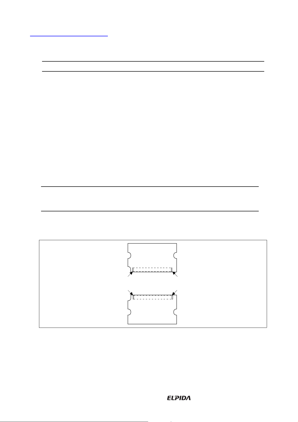
Pin Arrangement
Front Side
Back Side
2pin 144pin
1pin 143pin
查询"HB52D88GB-A6F"供应商
HB52D88GB-F
Data Sheet E0010H10
3
Pin Arrangement (cont.)
Front side Back side
Pin No. Signal name Pin No. Signal name Pin No. Signal name Pin No. Signal name
1VSS73 NC 2 V
SS
74 CK1
3 DQ0 75 V
SS
4 DQ32 76 V
SS
5 DQ1 77 NC 6 DQ33 78 NC
7 DQ2 79 NC 8 DQ34 80 NC
9 DQ3 81 V
CC
10 DQ35 82 V
CC
11 V
CC
83 DQ16 12 V
CC
84 DQ48
13 DQ4 85 DQ17 14 DQ36 86 DQ49
15 DQ5 87 DQ18 16 DQ37 88 DQ50
17 DQ6 89 DQ19 18 DQ38 90 DQ51
19 DQ7 91 V
SS
20 DQ39 92 V
SS
21 V
SS
93 DQ20 22 V
SS
94 DQ52
23 DQMB0 95 DQ21 24 DQMB4 96 DQ53
25 DQMB1 97 DQ22 26 DQMB5 98 DQ54
27 V
CC
99 DQ23 28 V
CC
100 DQ55
29 A0 101 V
CC
30 A3 102 V
CC
31 A1 103 A6 32 A4 104 A7
33 A2 105 A8 34 A5 106 A13 (BA0)
35 V
SS
107 V
SS
36 V
SS
108 V
SS
37 DQ8 109 A9 38 DQ40 110 A12 (BA1)
39 DQ9 111 A10 (AP) 40 DQ41 112 A11
41 DQ10 113 V
CC
42 DQ42 114 V
CC
43 DQ11 115 DQMB2 44 DQ43 116 DQMB6
45 V
CC
117 DQMB3 46 V
CC
118 DQMB7
47 DQ12 119 V
SS
48 DQ44 120 V
SS
49 DQ13 121 DQ24 50 DQ45 122 DQ56
51 DQ14 123 DQ25 52 DQ46 124 DQ57
53 DQ15 125 DQ26 54 DQ47 126 DQ58
55 V
SS
127 DQ27 56 V
SS
128 DQ59
57 NC 129 V
CC
58 NC 130 V
CC
59 NC 131 DQ28 60 NC 132 DQ60
61 CK0 133 DQ29 62 CKE0 134 DQ61
63 V
CC
135 DQ30 64 V
CC
136 DQ62
65 RE 137 DQ31 66 CE 138 DQ63
查询"HB52D88GB-A6F"供应商
HB52D88GB-F
Data Sheet E0010H10
4
Front side Back side
Pin No. Signal name Pin No. Signal name Pin No. Signal name Pin No. Signal name
67 W 139 V
SS
68 NC 140 V
SS
69 S0 141 SDA 70 NC 142 SCL
71 NC 143 V
CC
72 NC 144 V
CC
Pin Description
Pin name Function
A0 to A11 Address input
Row addressA0 to A11
Column address A0 to A8
A12/A13 Bank select address BA1, BA0
DQ0 to DQ63 Data-input/output
S0 Chip select
RE Row address asserted bank enable
CE Column address asserted
W Write enable
DQMB0 to DQMB7 Byte input/output mask
CK0/CK1 Clock input
CKE0 Clock enable
SDA Data-input/output for serial PD
SCL Clock input for serial PD
V
CC
Power supply
V
SS
Ground
NC No connection
查询"HB52D88GB-A6F"供应商
HB52D88GB-F
Data Sheet E0010H10
5
Serial PD Matrix*
1
Byte No. Function described Bit7 Bit6 Bit5 Bit4 Bit3 Bit2 Bit1 Bit0 Hex value Comments
0 Number of bytes used by
module manufacturer
1000000080 128
1 Total SPD memory size 0000100008 256 byte
2 Memory type 0000010004 SDRAM
3 Number of row addresses bits 000011000C 12
4 Numbe r of c ol umn addr es ses bi ts 0000100109 9
5 Number of banks 0000000101 1
6 Module data width 0100000040 64
7 Module data width (continued) 0000000000 0 (+)
8 Module interface signal levels 0000000101 LVTTL
9 SDRAM cycle time
(highest CE latency)
10 ns
10100000A0 CL = 3
10 SDRAM access from Clock
(highest CE latency)
6 ns
0110000060 CL = 3
11 Module configuration type 0000000000 Non parity
12 Refresh rate/type 1000000080 Normal
(15.625 µs)
Self refresh
13 SDRAM width 0001000010 8M × 16
14 Error checking SDRAM width 0000000000 —
15 SDRAM device attributes:
minimum clock delay for backto-back random column
addresses
0000000101 1 CLK
16 SDRAM device attributes:
Burst lengths supported
100011118F 1, 2, 4, 8, full
page
17 SDRAM device attributes:
number of banks on SDRAM
device
0000010004 4
18 SDRAM device attributes:
CE latency
0000011006 2, 3
19 SDRAM device attributes:
S latency
0000000101 0
20 SDRAM device attributes:
W latency
0000000101 0
21 SDRAM module attributes 0000000000 Unbuffer
22 SDRAM device attributes:
General
000011100E VCC ± 10%
查询"HB52D88GB-A6F"供应商
HB52D88GB-F
Data Sheet E0010H10
6
Byte No. Function described Bit7 Bit6 Bit5 Bit4 Bit3 Bit2 Bit1 Bit0 Hex value Comments
23 SDRAM cycle time
(2nd highest CE latency)
(-A6F/A6FL) 10 ns
10100000A0 CL=2
(-B6F/B6FL) 15 ns 11110000F0
24 SDRAM access from Clock
(2nd highest CE latency)
(-A6F/A6FL) 6 ns
0110000060 CL=2
(-B6F/B6FL) 8 ns 1000000080
25 SDRAM cycle time
(3rd highest CE latency)
Undefined
0000000000
26 SDRAM access from Clock
(3rd highest CE latency)
Undefined
0000000000
27 Minimum row precharge time 0001010014 20 ns
28 Row active to row active min 0001010014 20 ns
29 RE to CE delay min 0001010014 20 ns
30 Minimum RE pulse width 0011001032 50 ns
31 Density of each bank on
module
0001000010 64M byte
32 Address and command signal
input setup time
0010000020 2 ns
33 Address and command signal
input hold time
0001000010 1 ns
34 Data signal input setup time 0010000020 2 ns
35 Data signal input hold time 0001000010 1 ns
36 to 61 Superset information 0000000000 Future use
62 SPD data revision code 0001001012 Rev. 1.2A
63 Checksum for bytes 0 to 62
(-A6F/A6FL)
000011010D 13
(-B6F/B6FL) 011111017D 125
64 Manuf ac turer’ s JE DE C ID c ode0000011107 HITACHI
65 to 71 Manuf ac turer’ s JE DE C ID c ode0000000000
72 Manufacturing location ЧЧЧЧЧЧЧЧЧ× *3 (ASCII-
8bit code)
73 Manufacturer’s part number 0100100048 H
74 Manufacturer’s part number 0100001042 B
75 Manufacturer’s part number 0011010135 5
76 Manufacturer’s part number 0011001032 2
77 Manufacturer’s part number 0100010044 D
查询"HB52D88GB-A6F"供应商
HB52D88GB-F
Data Sheet E0010H10
7
Byte No. Function described Bit7 Bit6 Bit5 Bit4 Bit3 Bit2 Bit1 Bit0 Hex value Comments
78 Manufacturer’s part number 0011100038 8
79 Manufacturer’s part number 0011100038 8
80 Manufacturer’s part number 0100011147 G
81 Manufacturer’s part number 0100001042 B
82 Manufacturer’s part number 001011012D —
83 Manufacturer’s part number
(-A6F/A6FL)
0100000141 A
(-B6F/B6FL) 0100001042 B
84 Manufacturer’s part number 0011011036 6
85 Manufacturer’s part number 0100011046 F
86 Manufacturer’s part number
(L-version)
010011004C L
Manufacturer’s part number 0010000020 (Space)
87 Manufacturer’s part number 0010000020 (Space)
88 Manufacturer’s part number 0010000020 (Space)
89 Manufacturer’s part number 0010000020 (Space)
90 Manufacturer’s part number 0010000020 (Space)
91 Revision code 0011000030 Initial
92 Revision code 0010000020 (Space)
93 Manufacturing date ЧЧЧЧЧЧЧЧЧ× Year code
(BCD)*
4
94 Manufacturing date ЧЧЧЧЧЧЧЧЧ× Week code
(BCD)*
4
95 to 98 Assembly serial number *
6
99 to 125 Manufacturer specific data ————————— *
5
126 Intel specification frequency 0110010064 100 MHz
127 Intel specification CE# latency
support
(-A6F/A6FL)
11000111C7 CL = 2, 3
(-B6F/B6FL) 11000101C5 CL = 3
Notes: 1. All serial PD data are not protected. 0: Serial data, “driven Low”, 1: Serial data, “driven High”
These SPD are based on Intel specification (Rev.1.2A).
2. Regarding byte32 to 35, based on JEDEC Committee Ballot JC42.5-97-119.
3. Byte72 is manufacturing location code. (ex: In case of Japan, byte72 is 4AH. 4AH shows “J” on
ASCII code.)
4. Regarding byte93 and 94, based on JEDEC Committee Ballot JC42.5-97-135. BCD is “Binary
Coded Decimal”.
5. All bits of 99 through 125 are not defined (“1” or “0”).
6. Bytes 95 through 98 are assembly serial number.
查询"HB52D88GB-A6F"供应商

HB52D88GB-F
Data Sheet E0010H10
8
Block Diagram
DQMB0
DQ0 to DQ7
RAS (D0 to D3)
CAS (D0 to D3)
A0 to A11
A0 to A11 (D0 to D3)
CKE0
CKE (D0 to D3)
V
CC
V
CC
(D0 to D3, U0)
V
SS
V
SS
(D0 to D3, U0)
C100-C103
Serial PD
SDA
A0
A1
A2
V
SS
SCL
U0
SDA
SCL
Notes :
1. The SDA pull-up resistor is required due to
the open-drain/open-collector output.
2. The SCL pull-up resistor is recommended
because of the normal SCL line inacitve
"high" state.
CK0
CLK (D0)
8
N0, N1
DQMB1
DQ8 to DQ15
8
N2, N3
CLK (D1)
C0-C7
D0
CK1
CLK (D2)
CLK (D3)
RE
CE
A13 (D0 to D3)
BA1
A12 (D0 to D3)
BA0
W
S0
CS
DQMB4
DQ32 to DQ39
8
N8, N9
DQMB5
DQ40 to DQ47
8
N10, N11
D2
CS
DQMB2
DQ16 to DQ23
8
N4, N5
DQMB3
DQ24 to DQ31
8
N6, N7
D1
CS
DQMB6
DQ48 to DQ55
8
N12, N13
DQMB7
DQ56 to DQ63
8
N14, N15
D3
CS
* D0 to D3 : HM5212165
U0 : 2-kbit EEPROM
C0 to C7 : 0.33 µF
C100 to C103 : 0.1 µF
N0 to N15 : Network resistors (10 Ω)
查询"HB52D88GB-A6F"供应商

HB52D88GB-F
Data Sheet E0010H10
9
Absolute Maximum Ratings
Parameter Symbol Value Unit Note
Voltage on any pin relative to V
SS
V
T
–0.5 to VCC + 0.5
(≤ 4.6 (max))
V1
Supply voltage relative to V
SS
V
CC
–0.5 to +4.6 V 1
Short circuit output current Iout 50 mA
Power dissipation P
T
8.0 W
Operating temperature Topr 0 to +65 °C
Storage temperature Tstg –55 to +125 °C
Note: 1. Respect to VSS.
DC Operating Conditions (Ta = 0 to +65°C)
Parameter Symbol Min Max Unit Notes
Supply voltage V
CC
3.0 3.6 V 1, 2
V
SS
00V3
Input high voltage V
IH
2.0 VCC + 0.3 V 1, 4, 5
Input low voltage V
IL
–0.3 0.8 V 1, 6
Notes: 1. All voltage referred to V
SS
2. The supply voltage with all VCC pins must be on the same level.
3. The supply voltage with all V
SS pins must be on the same level.
4. CK, CKE, S, DQMB, DQ pins: V
IH
(max) = VCC + 0.5 V for pulse width ≤ 5 ns at VCC.
5. Others: V
IH
(max) = 4.6 V for pulse width ≤ 5 ns at VCC.
6. V
IL
(min) = –1.0 V for pulse width ≤ 5 ns at VSS.
查询"HB52D88GB-A6F"供应商

HB52D88GB-F
Data Sheet E0010H10
10
VIL/VIH Clamp (Component characteristic)
This SDRAM component has VIL and VIH clamp for CK, CKE, S, DQMB and DQ pins.
Minimum VIL Clamp Current
VIL (V) I (mA)
–2 –32
–1.8 –25
–1.6 –19
–1.4 –13
–1.2 –8
–1 –4
–0.9 –2
–0.8 –0.6
–0.6 0
–0.4 0
–0.2 0
00
VIL (V)
I (mA)
–1.5 –1 –0.5
–5
–15
–10
–25
–20
–30
0
–35
–2
0
查询"HB52D88GB-A6F"供应商

HB52D88GB-F
Data Sheet E0010H10
11
Minimum VIH Clamp Current
VIH (V) I (mA)
V
CC
+ 2 10
VCC + 1.8 8
VCC + 1.6 5.5
VCC + 1.4 3.5
VCC + 1.2 1.5
VCC + 1 0.3
VCC + 0.8 0
VCC + 0.6 0
VCC + 0.4 0
VCC + 0.2 0
VCC + 0 0
VIH (V)
V
CC
+ 0 VCC + 1 VCC + 2VCC + 0.5 VCC + 1.5
I (mA)
8
4
6
0
2
10
查询"HB52D88GB-A6F"供应商

HB52D88GB-F
Data Sheet E0010H10
12
IOL/IOH Characteristics (Component characteristic)
Output Low Current (IOL)
I
OL
I
OL
Vout (V) Min (mA) Max (mA)
00 0
0.4 27 71
0.65 41 108
0.85 51 134
1 58 151
1.4 70 188
1.5 72 194
1.65 75 203
1.8 77 209
1.95 77 212
3 80 220
3.45 81 223
I
OL
(mA)
Vout (V)
250
200
150
100
50
0
0 0.5 1 1.5 2 2.5 3 3.5
min
max
查询"HB52D88GB-A6F"供应商

HB52D88GB-F
Data Sheet E0010H10
13
Output High Current (IOH) (Ta = 0 to 65˚C, VCC = 3.0 V to 3.45 V, VSS = 0 V)
I
OH
I
OH
Vout (V) Min (mA) Max (mA)
3.45 — –3
3.3 — –28
3 0 –75
2.6 –21 –130
2.4 –34 –154
2 –59 –197
1.8 –67 –227
1.65 –73 –248
1.5 –78 –270
1.4 –81 –285
1 –89 –345
0 –93 –503
I
OH
(mA)
Vout (V)
0
–100
–200
–300
–500
–600
–400
0.5 1 1.5 2 2.5 3
min
max
3.50
查询"HB52D88GB-A6F"供应商

HB52D88GB-F
Data Sheet E0010H10
14
DC Characteristics (Ta = 0 to 65°C, VCC = 3.3 V ± 0.3 V, VSS = 0 V)
HB52D88GB
-A6F/B6F/A6FL/B6FL
Parameter Symbol Min Max Unit Test conditions Notes
Operating current I
CC1
— 480 mA Burst length = 1
t
RC
= min
1, 2, 3
Standby current in power down I
CC2P
— 12 mA CKE0 = VIL, tCK = 12 ns 6
Standby current in power down
(input signal stable)
I
CC2PS
— 8 mA CKE0 = VIL, tCK = ∞ 7
Standby current in non power
down
I
CC2N
— 60 mA CKE0, S = VIH,
t
CK
= 12 ns
4
Active standby current in power
down
I
CC3P
— 24 mA CKE0, S = VIH,
t
CK
= 12 ns
1, 2, 6
Active standby current in non
power down
I
CC3N
— 140 mA CKE0, S = VIH,
t
CK
= 12 ns
1, 2, 4
Burst operating current I
CC4
— 480 mA tCK = min, BL = 4 1, 2, 5
Refresh current I
CC5
— 880 mA tRC = min 3
Self refresh current I
CC6
— 8 mA VIH ≥ VCC – 0.2 V
V
IL
≤ 0.2 V
8
Self refresh current
(L-version)
I
CC6
— 6.4 mA
Input leakage current I
LI
–10 10 µA0 ≤ Vin ≤ V
CC
Output leakage current I
LO
–10 10 µA0 ≤ Vout ≤ V
CC
DQ = disable
Output high voltage V
OH
2.4 — V IOH = –4 mA
Output low voltage V
OL
— 0.4 V IOL = 4 mA
Notes: 1. ICC depends on output load condition when the device is selected. ICC (max) is specified at the
output open condition.
2. One bank operation.
3. Input signals are changed once per one clock.
4. Input signals are changed once per two clocks.
5. Input signals are changed once per four clocks.
6. After power down mode, CK0/CK1 operating current.
7. After power down mode, no CK0/CK1 operating current.
8. After self refresh mode set, self refresh current.
查询"HB52D88GB-A6F"供应商

HB52D88GB-F
Data Sheet E0010H10
15
Capacitance (Ta = 25°C, VCC = 3.3 V ± 0.3 V)
Parameter Symbol Max Unit Notes
Input capacitance (Address) C
IN
50 pF 1, 2, 4
Input capacitance (RE, CE, W, CK0/CK1, CKE0) C
IN
50 pF 1, 2, 4
Input capacitance (S0)C
IN
50 pF 1, 2, 4
Input capacitance (DQMB0 to DQMB7) C
IN
20 pF 1, 2, 4
Input/Output capacitance (DQ0 to DQ63) C
I/O
20 pF 1, 2, 3, 4
Notes: 1. Capacitance measured with Boonton Meter or effective capacitance measuring method.
2. Measurement condition: f = 1 MHz, 1.4 V bias, 200 mV swing.
3. DQMB = V
IH
to disable Data-out.
4. This parameter is sampled and not 100% tested.
查询"HB52D88GB-A6F"供应商

HB52D88GB-F
Data Sheet E0010H10
16
AC Characteristics (Ta = 0 to 65˚C, VCC = 3.3 V ± 0.3 V, VSS = 0 V)
HB52D88GB
-A6F/A6FL -B6F/B6FL
Parameter Symbol
PC100
Symbol Min Max Min Max Unit Notes
System clock cycle time
(CE latency = 2) t
CK
Tclk 10 — 15 — ns 1
(CE latency = 3) t
CK
Tclk 10 — 10 — ns
CK high pulse width t
CKH
Tch 3 — 3 — ns 1
CK low pulse width t
CKL
Tcl 3 — 3 — ns 1
Access time from CK
(CE latency = 2) t
AC
Tac — 6 — 8 ns 1, 2
(CE latency = 3) t
AC
Tac — 6 — 6 ns
Data-out hold time t
OH
Toh 3 — 3 — ns 1, 2
CK to Data-out low impedance t
LZ
2 — 2 — ns 1, 2, 3
CK to Data-out high impedance t
HZ
— 6 — 6 ns 1, 4
Data-in setup time tAS, tCS,
t
DS
, t
CES
Tsi 2 — 2 — ns 1, 5, 6
CKE setup time for power down
exit
t
CESP
Tpde 2 — 2 — ns 1
Data-in hold time tAH, tCH,
t
DH
, t
CEH
Thi 1 — 1 — ns 1, 5
Ref/Active to Ref/Active
command period
t
RC
Trc 70 — 70 — ns 1
Active to Precharge command
period
t
RAS
Tras 50 120000 50 120000 ns 1
Active command to column
command (same bank)
t
RCD
Trcd 20 — 20 — ns 1
Precharge to active command
period
t
RP
Trp 20 — 20 — ns 1
Write recovery or data-in to
precharge lead time
t
DPL
Tdpl 10 — 10 — ns 1
Active (a) to Active (b)
command period
t
RRD
Trrd 20 — 20 — ns 1
Transition time (rise and fall) t
T
1515ns
Refresh period t
REF
— 64 — 64 ms
查询"HB52D88GB-A6F"供应商

HB52D88GB-F
Data Sheet E0010H10
17
Notes: 1. AC measurement assumes tT = 1 ns. Reference level for timing of input signals is 1.5 V.
2. Access time is measured at 1.5 V. Load condition is CL = 50 pF.
3. t
LZ
(min) defines the time at which the outputs achieves the low impedance state.
4. t
HZ
(max) defines the time at which the outputs achieves the high impedance state.
5. t
CES
define CKE setup time to CK rising edge except power down exit command.
6. t
AS/tAH
: Address, tCS/tCH: S, RE, CE, W, DQMB
t
DS/tDH
: Data-in, t
CES/tCEH
: CKE
Test Conditions
• Input and output timing reference levels: 1.5 V
• Input waveform and output load: See following figures
t
T
2.4 V
0.4 V
0.8 V
2.0 V
input
t
T
I/O
CL
查询"HB52D88GB-A6F"供应商

HB52D88GB-F
Data Sheet E0010H10
18
Relationship Between Frequency and Minimum Latency
HB52D88GB
Parameter -A6F/A6FL/B6F/B6FL
Frequency (MHz) 100
tCK (ns) Symbol
PC100
Symbol 10 Notes
Active command to column command
(same bank)
l
RCD
21
Active command to active command
(same bank)
l
RC
7 = [l
RAS
+ lRP]
1
Active command to precharge command
(same bank)
l
RAS
51
Precharge command to active command
(same bank)
l
RP
21
Write recovery or data-in to precharge
command (same bank)
l
DPL
Tdpl 1 1
Active command to active command
(different bank)
l
RRD
21
Self refresh exit time l
SREX
Tsrx 1 2
Last data in to active command
(Auto precharge, same bank)
l
APW
Tdal 4 = [l
DPL
+ lRP]
Self refresh exit to command input l
SEC
7 = [lRC]
3
Precharge command to high impedance
(CE latency = 2) l
HZP
Troh 2
(CE latency = 3) l
HZP
Troh 3
Last data out to active command
(auto precharge) (same bank)
l
APR
1
Last data out to precharge (early precharge)
(CE latency = 2) l
EP
–1
(CE latency = 3) l
EP
–2
Column command to column command l
CCD
Tccd 1
Write command to data in latency l
WCD
Tdwd 0
DQMB to data in l
DID
Tdqm 0
DQMB to data out l
DOD
Tdqz 2
CKE to CK disable l
CLE
Tcke 1
Register set to active command l
RSA
Tmrd 1
查询"HB52D88GB-A6F"供应商

HB52D88GB-F
Data Sheet E0010H10
19
HB52D88GB
Parameter -A6F/A6FL/B6F/B6FL
Frequency (MHz) 100
tCK (ns) Symbol
PC100
Symbol 10 Notes
S to command disable l
CDD
0
Power down exit to command input l
PEC
1
Burst stop to output valid data hold
(CE latency = 2) l
BSR
1
(CE latency = 3) l
BSR
2
Burst stop to output high impedance
(CE latency = 2) l
BSH
2
(CE latency = 3) l
BSH
3
Burst stop to write data ignore l
BSW
0
Notes: 1. l
RCD
to l
RRD
are recommended value.
2. Be valid [DSEL] or [NOP] at next command of self refresh exit.
3. Except [DSEL] and [NOP].
查询"HB52D88GB-A6F"供应商

HB52D88GB-F
Data Sheet E0010H10
20
Pin Functions
CK0/CK1 (input pin): CK is the master clock input to this pin. The other input signals are referred at CK
rising edge.
S0 (input pin): When S is Low, the command input cycle becomes valid. When S is High, all inputs are
ignored. However, internal operations (bank active, burst operations, etc.) are held.
RE, CE and W (input pins): Although these pin names are the same as those of conventional DRAM
modules, they function in a different way. These pins define operation commands (read, write, etc.)
depending on the combination of their voltage levels. For details, refer to the command operation section.
A0 to A11 (input pins): Row address (AX0 to AX11) is determined by A0 to A11 level at the bank active
command cycle CK rising edge. Column address (AY0 to AY8) is determined by A0 to A8 level at the read
or write command cycle CK rising edge. And this column address becomes burst access start address. A10
defines the precharge mode. When A10 = High at the precharge command cycle, both banks are precharged.
But when A10 = Low at the precharge command cycle, only the bank that is selected by A12/A13 (BA) is
precharged.
A12/A13 (input pin): A12/A13 is a bank select signal (BA). The memory array is divided into bank0,
bank1, bank2 and bank3. If A12 is Low and A13 is Low, bank0 is selected. If A12 is High and A13 is Low,
bank1 is selected. If A12 is Low and A13 is High, bank2 is selected. If A12 is High and A13 is HIgh, bank3
is selected.
CKE0, CKE1 (input pin): This pin determines whether or not the next CK is valid. If CKE is High, the
next CK rising edge is valid. If CKE is Low, the next CK rising edge is invalid. This pin is used for powerdown and clock suspend modes.
DQMB0 to DQMB7 (input pins): Read operation: If DQMB is High, the output buffer becomes High-Z. If
the DQMB is Low, the output buffer becomes Low-Z.
Write operation: If DQMB is High, the previous data is held (the new data is not written). If DQMB is Low,
the data is written.
DQ0 to DQ63 (DQ pins): Data is input to and output from these pins.
VCC (power supply pins): 3.3 V is applied.
VSS (power supply pins): Ground is connected.
Detailed Operation Part
Refer to the HM5212165F/HM5212805F-75/A60/B60 datasheet.
查询"HB52D88GB-A6F"供应商

HB52D88GB-F
Data Sheet E0010H10
21
Physical Outline
0.80 ± 0.08
Detail A
3.80 Max
1.0 ± 0.08
0.50
0.37 ± 0.03
Detail B
4-R1.0 ± 0.1
R1.0 ± 0.1
5.0 ± 0.1
2.00 Min
0.25 Max
3.5 Min
3.5 Min
2.5 Min
30.0
15.0
42.0 Max
1.0 Min
(38.0)
35.50
37.0 ± 0.08
35.50
17.625
17.875
0.875
0.625
1.0 Min
1.0 Min 1.0 Min
Unit: mm
4.0 ± 0.1
1
2
B
,,,,,,,,,,,,,,,,,,,,
,
,,,,,,,,,,,,,,,,,,,,
,
,,,,,,,,,,,,,,,,,,,,
,
,,,,,,,,,,,,,,,,,,,,
,
,,,,,,,,,,,,,,,,,,,,
,
,,,,,,,,,,,,,,,,,,,,
,
,,,,,,,,,,,,,,,,,,,,
,
,,,,,,,,,,,,,,,,,,,,
,
,,,,,,,,,,,,,,,,,,,,
,
,,,,,,,,,,,,,,,,,,,,
,
,,,,,,,,,,,,,,,,,,,,
,
Component area
(front)
A
,,,,,,,,,,,,,,,,,,,,
,
,,,,,,,,,,,,,,,,,,,,
,
,,,,,,,,,,,,,,,,,,,,
,
,,,,,,,,,,,,,,,,,,,,
,
,,,,,,,,,,,,,,,,,,,,
,
,,,,,,,,,,,,,,,,,,,,
,
,,,,,,,,,,,,,,,,,,,,
,
,,,,,,,,,,,,,,,,,,,,
,
,,,,,,,,,,,,,,,,,,,,
,
,,,,,,,,,,,,,,,,,,,,
,
,,,,,,,,,,,,,,,,,,,,
,
Component area
(back)
查询"HB52D88GB-A6F"供应商

HB52D88GB-F
Data Sheet E0010H10
22
Cautions
1. Elpida Memory, Inc. neither warrants nor grants licenses of any rights of Elpida Memory, Inc.’s or any
third party’s patent, copyright, trademark, or other intellectual property rights for information contained in
this document. Elpida Memory, Inc. bears no responsibility for problems that may arise with third party’s
rights, including intellectual property rights, in connection with use of the information contained in this
document.
2. Products and product specifications may be subject to change without notice. Confirm that you have
received the latest product standards or specifications before final design, purchase or use.
3. Elpida Memory, Inc. makes every attempt to ensure that its products are of high quality and reliability.
However, contact Elpida Memory, Inc. before using the product in an application that demands especially
high quality and reliability or where its failure or malfunction may directly threaten human life or cause
risk of bodily injury, such as aerospace, aeronautics, nuclear power, combustion control, transportation,
traffic, safety equipment or medical equipment for life support.
4. Design your application so that the product is used within the ranges guaranteed by Elpida Memory, Inc.
particularly for maximum rating, operating supply voltage range, heat radiation characteristics, installation
conditions and other characteristics. Elpida Memory, Inc. bears no responsibility for failure or damage
when used beyond the guaranteed ranges. Even within the guaranteed ranges, consider normally
foreseeable failure rates or failure modes in semiconductor devices and employ systemic measures such as
fail-safes, so that the equipment incorporating Elpida Memory, Inc. product does not cause bodily injury,
fire or other consequential damage due to operation of the Elpida Memory, Inc. product.
5. This product is not designed to be radiation resistant.
6. No one is permitted to reproduce or duplicate, in any form, the whole or part of this document without
written approval from Elpida Memory, Inc..
7. Contact Elpida Memory, Inc. for any questions regarding this document or Elpida Memory, Inc.
semiconductor products.
查询"HB52D88GB-A6F"供应商

查询"HB52D88GB-A6F"供应商
This datasheet has been downloaded from:
www.EEworld.com.cn
Free Download
Daily Updated Database
100% Free Datasheet Search Site
100% Free IC Replacement Search Site
Convenient Electronic Dictionary
Fast Search System
www.EEworld.com.cn
All Datasheets Cannot Be Modified Without Permission
Copyright © Each Manufacturing Company
 Loading...