

ELPIDA EDE2104ABSE, EDE2108ABSE DATA SHEET

PRELIMINARY DATA SHEET
2G bits DDR2 SDRAM
EDE2104ABSE (512M words × 4 bits)
EDE2108ABSE (256M words × 8 bits)
Specifications
• Density: 2G bits
• Organization
⎯ 64M words × 4 bits × 8 banks (EDE2104ABSE)
⎯ 32M words × 8 bits × 8 banks (EDE2108ABSE)
• Package
⎯ 68-ball FBGA
⎯ Lead-free (RoHS compliant)
• Power supply: VDD, VDDQ = 1.8V ± 0.1V
• Data rate
⎯ 800Mbps/667Mbps/533Mbps (max.)
• 1KB page size
⎯ Row address: A0 to A14
⎯ Column address: A0 to A9, A11 (EDE2104ABSE)
A0 to A9 (EDE2108ABSE)
• Eight internal banks for concurrent operation
• Interface: SSTL_18
• Burst lengths (BL): 4, 8
• Burst type (BT):
⎯ Sequential (4, 8)
⎯ Interleave (4, 8)
• /CAS Latency (CL): 3, 4, 5, 6
• Precharge: auto precharge option for each burst
access
• Driver strength: normal/weak
• Refresh: auto-refresh, self-refresh
• Refresh cycles: 8192 cycles/64ms
⎯ Average refresh period
7.8μs at 0°C ≤ TC ≤ +85°C
3.9μs at +85°C < TC ≤ +95°C
• Operating case temperature range
⎯ TC = 0°C to +95°C
Features
• Double-data-rate architecture; two data transfers per
clock cycle
• The high-speed data transfer is realized by the 4 bits
prefetch pipelined architecture
• Bi-directional differential data strobe (DQS and /DQS)
is transmitted/received with data for capturing data at
the receiver
• DQS is edge-aligned with data for READs; centeraligned with data for WRITEs
• Differential clock inputs (CK and /CK)
• DLL aligns DQ and DQS transitions with CK
transitions
• Commands entered on each positive CK edge; data
and data mask referenced to both edges of DQS
• Data mask (DM) for write data
• Posted /CAS by programmable additive latency for
better command and data bus efficiency
• Off-Chip-Driver Impedance Adjustment and On-DieTermination for better signal quality
• Programmable RDQS, /RDQS output for making × 8
organization compatible to × 4 organization
• /DQS, (/RDQS) can be disabled for single-ended
Data Strobe operation
Document No. E1196E10 (Ver. 1.0)
Date Published November 2007 (K) Japan
Printed in Japan
URL: http://www.elpida.com
©Elpida Memory, Inc. 2007
Ordering Information
Part number
EDE2104ABSE-8G-E
EDE2104ABSE-6E-E
EDE2104ABSE-5C-E
EDE2108ABSE-8G-E
EDE2108ABSE-6E-E
EDE2108ABSE-5C-E
Part Number
Elpida Memory
Type
D: Monolithic Device
Product Family
E: DDR2
Density / Bank
21: 2Gb / 8-bank
Organization
04: x4
08: x8
Power Supply, Interface
A: 1.8V, SSTL_18
Mask
version
B 512M × 4 8
256M × 8
EDE2104ABSE, EDE2108ABSE
Organization
(words × bits)
Internal
Banks
Speed bin
(CL-tRCD-tRP)
DDR2-800 (6-6-6)
DDR2-667 (5-5-5)
DDR2-533 (4-4-4)
DDR2-800 (6-6-6)
DDR2-667 (5-5-5)
DDR2-533 (4-4-4)
E D E 21 04 A B SE - 8G - E
Speed
8G DDR2-800 (6-6-6)
6E: DDR2-667 (5-5-5)
5C: DDR2-533 (4-4-4)
Package
SE: FBGA
Die Rev.
Package
68-ball FBGA
Environment code
E: Lead Free
(RoHS compliant)
Preliminary Data Sheet E1196E10 (Ver. 1.0)
2
Pin Configurations
/xxx indicates active low signal.
EDE2104ABSE, EDE2108ABSE
68-ball FBGA
(×8, ×4 organization)
2
1
A
NC
B
C
D
3
7
8
9
NC
NCNC
E
F
G
H
J
K
L
M
N
P
R
T
U
V
W
Note: ( )* marked pins are for ×4 organization.
VDD
DQ6
(NC)*
VDDQ
DQ4
(NC)*
VDDL
BA2
VSS
VDD
NC
NU/ /RDQS
VSS
(NC)*
DM/RDQS
VSSQ
(DM)*
DQ1
VDDQ
VSSQ
DQ3
VREF
VSS
CKE
/WE
BA0
BA1
A10
A1
A3
A5
A7
A9
A12
A14
NC NC NC
(Top view)
VSSQ
DQS
VDDQ
DQ2
VSSDL
/RAS
/CAS
A2
A6
A11
NC
/DQS
VSSQ
DQ0
VSSQ
CK
/CK
/CS
A0
A4
A8
A13
VDDQ
DQ7
(NC)*
VDDQ
DQ5
(NC)*
VDD
ODT
VDD
VSS
Pin name Function Pin name Function
A0 to A14 Address inputs ODT ODT control
BA0, BA1, BA2 Bank select VDD Supply voltage for internal circuit
DQ0 to DQ7 Data input/output VSS Ground for internal circuit
DQS, /DQS Differential data strobe VDDQ Supply voltage for DQ circuit
RDQS, /RDQS Differential data strobe for read VSSQ Ground for DQ circuit
/CS Chip select VREF Input reference voltage
/RAS, /CAS, /WE Command input VDDL Supply voltage for DLL circuit
CKE Clock enable VSSDL Ground for DLL circuit
CK, /CK Differential clock input NC*1 No connection
DM Write data mask NU*2 Not usable
Notes: 1. Not internally connected with die.
2. Don’t connect. Internally connected.
Preliminary Data Sheet E1196E10 (Ver. 1.0)
3

CONTENTS
EDE2104ABSE, EDE2108ABSE
Specifications.................................................................................................................................................1
Features.........................................................................................................................................................1
Ordering Information......................................................................................................................................2
Part Number ..................................................................................................................................................2
Pin Configurations.........................................................................................................................................3
Electrical Specifications.................................................................................................................................5
Block Diagram .............................................................................................................................................29
Pin Function.................................................................................................................................................30
Command Operation...................................................................................................................................32
Simplified State Diagram.............................................................................................................................40
Operation of DDR2 SDRAM........................................................................................................................41
Package Drawing ........................................................................................................................................78
Recommended Soldering Conditions..........................................................................................................79
Preliminary Data Sheet E1196E10 (Ver. 1.0)
4
EDE2104ABSE, EDE2108ABSE
Electrical Specifications
• All voltages are referenced to VSS (GND)
• Execute power-up and Initialization sequence before proper device oper ation is achieved.
Absolute Maximum Ratings
Parameter Symbol Rating Unit Notes
Power supply voltage VDD −1.0 to +2.3 V 1
Power supply voltage for output VDDQ −0.5 to +2.3 V 1
Input voltage VIN −0.5 to +2.3 V 1
Output voltage VOUT −0.5 to +2.3 V 1
Storage temperature Tstg −55 to +100 °C 1, 2
Power dissipation PD 1.0 W 1
Short circuit output current IOUT 50 mA 1
Notes: 1. Stresses greater than those listed under Absolute Maximum Ratings may cause permanent damage to
the device. This is a stress rating only and functional operation of the device at these or any other
conditions above those indicated in the operational sections of this spec ification is not implied. E xposure
to absolute maximum rating conditions for extended periods may affect reliability.
2. Storage temperature is the case surface temperature on the center/top side of the DRAM.
Caution
Exposing the device to stress above those listed in Absolute Maximum Ratings could cause
permanent damage. The device is not meant to be operated under conditions outside the limits
described in the operational section of this specification. Exposure to Absolute Maximum Rating
conditions for extended periods may affect device reliability.
Operating Temperature Condition
Parameter Symbol Rating Unit Notes
Operating case temperature TC 0 to +95 °C 1, 2
Notes: 1. Operating temperature is the case surface temperature on the center/top side of the DRAM.
2. Supporting 0°C to +85°C with full AC and DC specifications.
Supporting 0°C to +85°C and being able to extend to +95°C with doubling auto-refresh commands in
frequency to a 32ms period (tREFI = 3.9µs) and higher temperature Self-Refresh entry via A7 "1" on
EMRS (2).
Preliminary Data Sheet E1196E10 (Ver. 1.0)
5
EDE2104ABSE, EDE2108ABSE
Recommended DC Operating Conditions (SSTL_18)
Parameter Symbol min. typ. max. Unit Notes
Supply voltage VDD 1.7 1.8 1.9 V 4
Supply voltage for output VDDQ 1.7 1.8 1.9 V 4
Input reference voltage VREF 0.49 × VDDQ 0.50 × VDDQ 0.51 × VDDQ V 1, 2
Termination voltage VTT VREF − 0.04 VREF VREF + 0.04 V 3
DC input logic high VIH (DC) VREF + 0.125 ⎯ VDDQ + 0.3 V
DC input low VIL (DC) −0.3 ⎯ VREF – 0.125 V
AC input logic high
-8G, -6E
-5C VIH (AC) VREF + 0.250 ⎯ ⎯ V
AC input low
-8G, -6E
-5C VIL (AC) ⎯ ⎯ VREF − 0.250 V
Notes: 1. The value of VREF may be selected by the user to provide optimum noise margin in the system. Typically
the value of VREF is expected to be about 0.5 × VDDQ of the transmitting device and VREF are expected
to track variations in VDDQ.
2. Peak to peak AC noise on VREF may not exceed ±2% VREF (DC).
3. VTT of transmitting device must track VREF of receiving device.
4. VDDQ tracks with VDD, VDDL tracks with VDD. AC parameters are measured with VDD, VDDQ and
VDDL tied together.
VIH (AC) VREF + 0.200 ⎯ ⎯ V
VIL (AC) ⎯ ⎯ VREF – 0.200 V
Preliminary Data Sheet E1196E10 (Ver. 1.0)
6
EDE2104ABSE, EDE2108ABSE
AC Overshoot/Undershoot Specification
Parameter Pins Specification Unit
Maximum peak amplitude allowed for overshoot
Maximum peak amplitude allowed for undershoot 0.5 V
Maximum overshoot area above VDD
DDR2-800
DDR2-667 0.8 V-ns
DDR2-533 1.0 V-ns
Maximum undershoot area below VSS
DDR2-800
DDR2-667 0.8 V-ns
DDR2-533 1.0 V-ns
Maximum peak amplitude allowed for overshoot CK, /CK 0.5 V
Maximum peak amplitude allowed for undershoot 0.5 V
Maximum overshoot area above VDD
DDR2-800, 667
DDR2-533 0.28 V-ns
Maximum undershoot area below VSS
DDR2-800, 667
DDR2-533 0.28 V-ns
Maximum peak amplitude allowed for overshoot DQ, DQS, /DQS, 0.5 V
Maximum peak amplitude allowed for undershoot RDQS, /RDQS, DM 0.5 V
Maximum overshoot area above VDDQ
DDR2-800, 667
DDR2-533 0.28 V-ns
Maximum undershoot area below VSSQ
DDR2-800, 667
DDR2-533 0.28 V-ns
Command, Address,
CKE, ODT
0.66 V-ns
0.66 V-ns
0.23 V-ns
0.23 V-ns
0.23 V-ns
0.23 V-ns
0.5 V
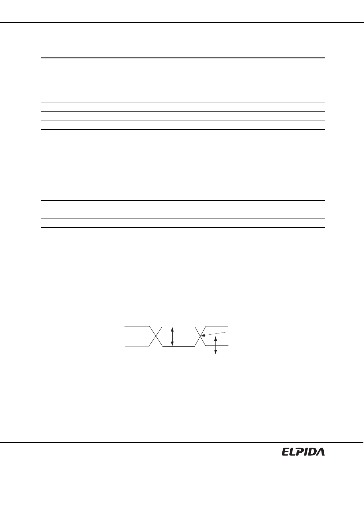
Volts (V)
VDD, VDDQ
VSS, VSSQ
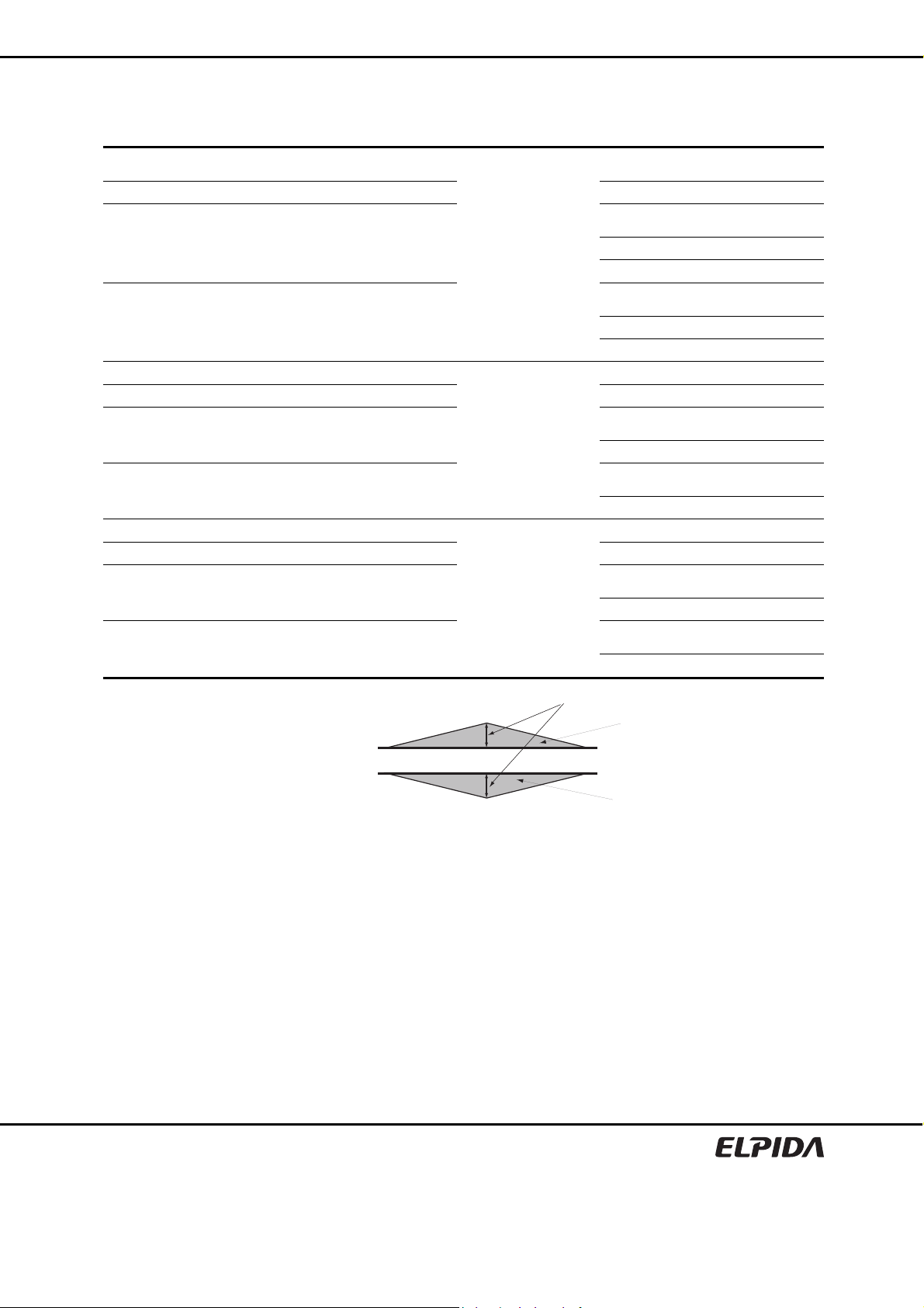
Overshoot/Undershoot Definition
Time (ns)
Maximum amplitude
Overshoot area
Undershoot area
Preliminary Data Sheet E1196E10 (Ver. 1.0)
7
EDE2104ABSE, EDE2108ABSE
DC Characteristics 1 (TC = 0°C to +85°C, VDD, VDDQ = 1.8V ± 0.1V)
max.
Parameter Symbol Grade
Operating current
(ACT-PRE)
Operating current
(ACT-READ-PRE)
Precharge powerdown standby current
Precharge quiet
standby current
Idle standby current IDD2N
Active power-down
standby current
Active standby current IDD3N
Operating current
(Burst read operating)
Operating current
(Burst write operating)
IDD0
IDD1
IDD2P
IDD2Q
IDD3P-F
IDD3P-S
IDD4R
IDD4W
-8G
-6E
-5C
-8G
-6E
-5C
-8G
-6E
-5C
-8G
-6E
-5C
-8G
-6E
-5C
-8G
-6E
-5C
-8G
-6E
-5C
-8G
-6E
-5C
-8G
-6E
-5C
-8G
-6E
-5C
× 4 × 8
TBD
TBD
TBD
TBD
TBD
TBD
TBD
TBD
TBD
TBD
TBD
TBD
TBD
TBD
TBD
TBD
TBD
TBD
TBD
TBD
TBD
TBD
TBD
TBD
TBD
TBD
TBD
TBD
TBD
TBD
TBD
TBD
TBD
TBD
TBD
TBD
TBD
TBD
TBD
TBD
TBD
TBD
TBD
TBD
TBD
TBD
TBD
TBD
TBD
TBD
TBD
TBD
TBD
TBD
TBD
TBD
TBD
TBD
TBD
TBD
Unit Test condition
one bank; tCK = tCK (IDD), tRC = tRC (IDD),
tRAS = tRAS min.(IDD);
mA
CKE is H, /CS is H between valid commands;
Address bus inputs are SWITCHING;
Data bus inputs are SWITCHING
one bank; IOUT = 0mA;
BL = 4, CL = CL(IDD), AL = 0;
tCK = tCK (IDD), tRC = tRC (IDD),
mA
tRAS = tRAS min.(IDD); tRCD = tRCD (IDD);
CKE is H, /CS is H between valid commands;
Address bus inputs are SWITCHING;
Data pattern is same as IDD4W
all banks idle;
tCK = tCK (IDD);
mA
CKE is L;
Other control and address bus inputs are STABLE;
Data bus inputs are FLOATING
all banks idle;
tCK = tCK (IDD);
mA
CKE is H, /CS is H;
Other control and address bus inputs are STABLE;
Data bus inputs are FLOATING
all banks idle;
tCK = tCK (IDD);
mA
CKE is H, /CS is H;
Other control and address bus inputs are SWITCHING;
Data bus inputs are SWITCHING
all banks open;
tCK = tCK (IDD);
mA
CKE is L;
Other control and address
bus inputs are STABLE;
mA
Data bus inputs are
FLOATING
all banks open;
tCK = tCK (IDD), tRAS = tRAS max.(IDD), tRP = tRP (IDD);
mA
CKE is H, /CS is H between valid commands;
Other control and address bus inputs are SWITCHING;
Data bus inputs are SWITCHING
all banks open, continuous burst reads, IOUT = 0mA;
BL = 4, CL = CL(IDD), AL = 0;
tCK = tCK (IDD), tRAS = tRAS max.(IDD), tRP = tRP (IDD);
mA
CKE is H, /CS is H between valid commands;
Address bus inputs are SWITCHING;
Data pattern is same as IDD4W
all banks open, continuous burst writes;
BL = 4, CL = CL(IDD), AL = 0;
tCK = tCK (IDD), tRAS = tRAS max.(IDD), tRP = tRP (IDD);
mA
CKE is H, /CS is H between valid commands;
Address bus inputs are SWITCHING;
Data bus inputs are SWITCHING
Fast PDN Exit
MRS (12) = 0
Slow PDN Exit
MRS (12) = 1
Preliminary Data Sheet E1196E10 (Ver. 1.0)
8
EDE2104ABSE, EDE2108ABSE
max.
Parameter Symbol Grade
-8G
Auto-refresh current IDD5
Self-refresh current IDD6 TBD TBD mA
Operating current
(Bank interleaving)
IDD7
-6E
-5C
-8G
-6E
-5C
× 4 × 8
TBD
TBD
TBD
TBD
TBD
TBD
Notes: 1. IDD specifications are tested after the device is properly initialized.
2. Input slew rate is specified by AC Input Test Condition.
3. IDD parameters are specified with ODT disabled.
4. Data bus consists of DQ, DM, DQS, /DQS, RDQS and /RDQS. IDD values must be met with all
combinations of EMRS bits 10 and 11.
5. Definitions for IDD
L is defined as VIN ≤ VIL (AC) (max.)
H is defined as VIN ≥ VIH (AC) (min.)
STABLE is defined as inputs stable at an H or L level
FLOATING is defined as inputs at VREF = VDDQ/2
SWITCHING is defined as:
inputs changing between H and L every other clock cycle (once per two clocks) for address and control
signals, and inputs changing between H and L every other data transfer (once per clock) for DQ sign als
not including masks or strobes.
6. Refer to AC Timing for IDD Test Conditions.
TBD
TBD
TBD
TBD
TBD
TBD
Unit Test condition
tCK = tCK (IDD);
Refresh command at every tRFC (IDD) interval;
mA
CKE is H, /CS is H between valid commands;
Other control and address bus inputs are SWITCHING;
Data bus inputs are SWITCHING
Self-Refresh Mode;
CK and /CK at 0V;
CKE ≤ 0.2V;
Other control and address bus inputs are FLOATING;
Data bus inputs are FLOATING
all bank interleaving reads, IOUT = 0mA;
BL = 4, CL = CL(IDD), AL = tRCD (IDD) −1
tCK = tCK (IDD), tRC = tRC (IDD), tRRD = tRRD (IDD),
tFAW = tFAW (IDD), tRCD = 1
mA
CKE is H, /CS is H between valid commands;
Address bus inputs are STABLE during DESELECTs;
Data pattern is same as IDD4W;
× tCK (IDD);
× tCK (IDD);
Preliminary Data Sheet E1196E10 (Ver. 1.0)
9
EDE2104ABSE, EDE2108ABSE
AC Timing for IDD Test Conditions
For purposes of IDD testing, the following parameters are to be utilized.
Parameter 6-6-6 5-5-5 4-4-4
CL (IDD) 6 5 4 tCK
tRCD (IDD) 15 15 15 ns
tRC (IDD) 60 60 60 ns
tRRD (IDD) 7.5 7.5 7.5 ns
tFAW (IDD) 35 37.5 37.5 ns
tCK (IDD) 2.5 3 3.75 ns
tRAS (min.)(IDD) 45 45 45 ns
tRAS (max.)(IDD) 70000 70000 70000 ns
tRP (IDD) 15 15 15 ns
tRFC (IDD) 195 195 195 ns
IDD7 Timing Patterns for 8 Banks
The detailed timings are shown in the IDD7 Timing Patterns for 8 Banks tables.
Speed bins Timing Patterns
DDR2-533 A0 RA0 A1 RA1 A2 RA2 A3 RA3 D D A4 RA4 A5 RA5 A6 RA6 A7 RA7 D D
DDR2-667 A0 RA0 D A1 RA1 D A2 RA2 D A3 RA3 D D A4 RA4 D A5 RA5 D A6 RA6 D A7 RA7 D D
DDR2-800 A0 RA0 D A1 RA1 D A2 RA2 D A3 RA3 D D D A4 RA4 D A5 RA5 D A6 RA6 D A7 RA7 D D D
Remark: A = Active. RA = Read with auto precharge. D = Deselect
Notes: 1. All banks are being interleaved at minimum tRC (IDD) without violating tRRD (IDD) and tFAW (IDD) using
a Burst length = 4.
2. Control and address bus inputs are STABLE during DESELECTs.
3. IOUT = 0mA.
DDR2-800 DDR2-667 DDR2-533
Unit
Preliminary Data Sheet E1196E10 (Ver. 1.0)
10
EDE2104ABSE, EDE2108ABSE
DC Characteristics 2 (TC = 0°C to +85°C, VDD, VDDQ = 1.8V ± 0.1V)
Parameter Symbol Value Unit Notes
Input leakage current ⏐ILI⏐ 2 μA VDD ≥ VIN ≥ VSS
Output leakage current ⏐ILO⏐ 5 μA VDDQ ≥ VOUT ≥ VSS
Minimum required output pull-up under AC
test load
Maximum required output pull-down under
AC test load
Output timing measurement reference level VOTR 0.5 × VDDQ V 1
Output minimum sink DC current IOL +13.4 mA 3, 4, 5
Output minimum source DC current IOH −13.4 mA 2, 4, 5
Notes: 1. The VDDQ of the device under test is referenced.
2. VDDQ = 1.7V; VOUT = 1.42V.
3. VDDQ = 1.7V; VOUT = 0.28V.
4. The DC value of VREF applied to the receiving device is expected to be set to VTT.
5. After OCD calibration to 18Ω at TC = 25°C, VDD = VDDQ = 1.8V.
DC Characteristics 3 (TC = 0°C to +85°C, VDD, VDDQ = 1.8V ± 0.1V)
VOH VTT + 0.603 V 5
VOL VTT − 0.603 V 5
Parameter Symbol min. max. Unit Notes
AC differential input voltage VID (AC) 0.5 VDDQ + 0.6 V 1, 2
AC differential cross point voltage VIX (AC) 0.5 × VDDQ − 0.175 0.5 × VDDQ + 0.175 V 2
AC differential cross point voltage VOX (AC) 0.5 × VDDQ − 0.125 0.5 × VDDQ + 0.125 V 3
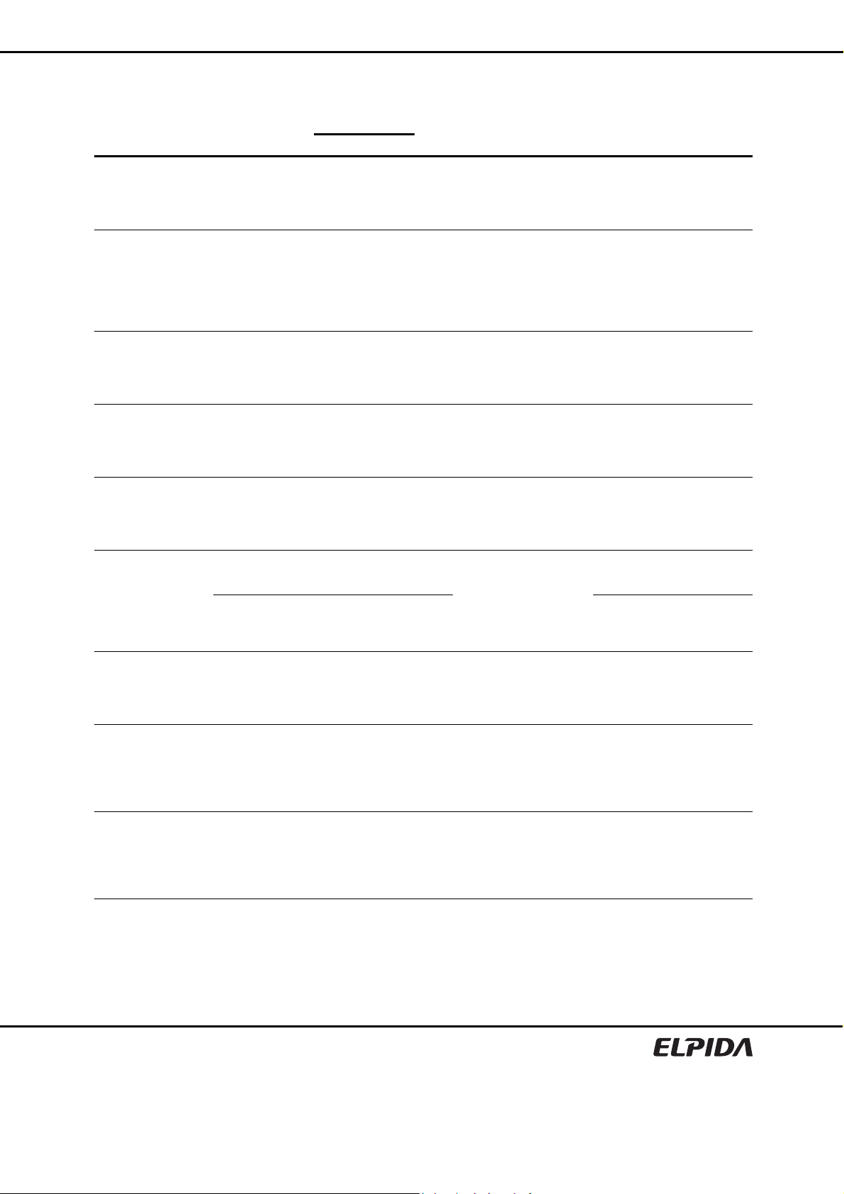
Notes: 1. VID (AC) specifies the input differential voltage |VTR -VCP | required for switching, where VT R is the true
input signal (such as CK, DQS, RDQS) and VCP is the complementary input signal (such as /CK, /DQS,
/RDQS). The minimum value is equal to VIH (AC) − VIL (AC).
2. T he typical value of VIX (A C) is expected to be about 0.5 × VDDQ of the transmitting device and VIX (AC)
is expected to track variations in VDDQ. VIX (AC) indicates the voltage at which differential input sig nals
must cross.
3. The typical value of VOX (AC) is expected to be about 0.5 × VDDQ of the transmitting device and
VOX (AC) is expected to track variations in VDDQ. VOX (AC) indicates the voltage at which differential
output signals must cross.
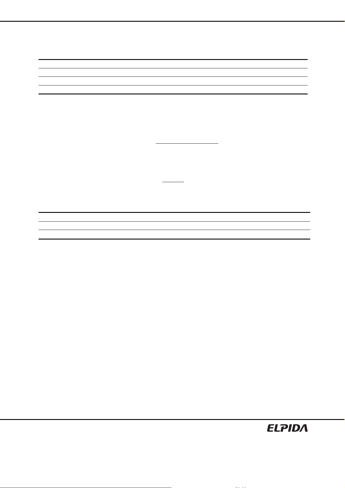
VDDQ
VTR
VID
VCP
VSSQ
Differential Signal Levels*
VIX or VOX
1, 2
Crossing point
Preliminary Data Sheet E1196E10 (Ver. 1.0)
11
EDE2104ABSE, EDE2108ABSE
ODT DC Electrical Characteristics (TC = 0°C to +85°C, VDD, VDDQ = 1.8V ± 0.1V)
Parameter Symbol min. typ. max. Unit Note
Rtt effective impedance value for EMRS (A6, A2) = 0, 1; 75 Ω Rtt1 (eff) 60 75 90 Ω 1
Rtt effective impedance value for EMRS (A6, A2) = 1, 0; 150 Ω Rtt2 (eff) 120 150 180 Ω 1
Rtt effective impedance value for EMRS (A6, A2) = 1, 1; 50 Ω Rtt3 (eff) 40 50 60 Ω 1
Deviation of VM with respect to VDDQ/2 ΔVM −6 ⎯ +6 % 1
Note: 1. Test condition for Rtt measurements.
Measurement Definition for Rtt (eff)
Apply VIH (AC) and VIL (AC) to test pin separately, then measure current I(VIH(AC)) and I(VIL(AC)) respectively.
VIH(AC), and VDDQ values defined in SSTL_18.
)()(
ACVILACVIH
)(
effRtt
=
Measurement Definition for ΔVM
Measure voltage (VM) at test pin (midpoint) with no load.
⎛
=Δ
VM
⎜
VDDQ
⎝
×
VM
−
−
⎞
1001 - 2×
⎟
⎠
))(())((
ACVILIACVIHI
OCD Default Characteristics (TC = 0°C to +85°C, VDD, VDDQ = 1.8V ± 0.1V)
Parameter min. typ. max. Unit Notes
Output impedance 12.6 18 23.4 Ω 1, 5
Pull-up and pull-down mismatch 0 ⎯ 4 Ω 1, 2
Output slew rate 1.5 ⎯ 5 V/ns 3, 4
Notes: 1. Impedance measurement condition for output source DC current: VDDQ = 1.7V; VOUT = 1420mV;
(VOUT−VDDQ)/IOH must be less than 23.4Ω for values of VOUT between VDDQ and VDDQ −280mV.
Impedance measurement condition for output sink DC current: VDDQ = 1.7V; VOUT = 280mV;
VOUT/IOL must be less than 23.4Ω for values of VOUT between 0V and 280mV.
2. Mismatch is absolute value between pull up and pull down, both are measured at same temperature and
voltage.
3. Slew rate measured from VIL(AC) to VIH(AC).
4. The absolute value of the slew rate as measured from DC to DC is equal to or greater than the slew rate
as measured from AC to AC. This is guaranteed by design and characterization.
5. DRAM I/O specifications for timing, voltage, and slew rate are no longer applicable if OCD is changed
from default settings.
Preliminary Data Sheet E1196E10 (Ver. 1.0)
12
EDE2104ABSE, EDE2108ABSE
Pin Capacitance (TA = 25°C, VDD, VDDQ = 1.8V ± 0.1V)
Parameter Symbol Pins min. max. Unit Notes
CLK input pin capacitance CCK CK, /CK 1.0 2.0 pF 1
Input pin capacitance
-8G
-6E, -5C
Input/output pin capacitance
-8G, -6E
-5C
CIN
CI/O
Notes: 1. Matching within 0.25pF.
2. Matching within 0.50pF.
/RAS, /CAS,
/WE, /CS,
CKE, ODT,
Address
DQ, DQS, /DQS,
RDQS, /RDQS, DM
1.0 1.75 pF 1
1.0 2.0 pF 1
2.5 3.5 pF 2
2.5 4.0 pF 2
Preliminary Data Sheet E1196E10 (Ver. 1.0)
13
EDE2104ABSE, EDE2108ABSE
AC Characteristics (TC = 0°C to +85°C, VDD, VDDQ = 1.8V ± 0.1V, VSS, VSSQ = 0V) [DDR2-800, 667]
• New units tCK(avg) and nCK, are introduced in DDR2-800 and DDR2-667
tCK(avg): actual tCK(avg) of the input clock under operation.
nCK: one clock cycle of the input clock, counting the actual clock edges.
-8G -6E
Speed bin DDR2-800 (6-6-6) DDR2-667 (5-5-5)
Parameter Symbol min. max. min. max. Unit Notes
Active to read or write command
delay
Precharge command period tRP 15 ⎯ 15 ⎯ ns
Active to active/auto-refresh
command time
DQ output access time from CK, /CK tAC −400 +400 −450 +450 ps 10
DQS output access time from CK,
/CK
CK high-level width tCH (avg) 0.48 0.52 0.48 0.52
CK low-level width tCL(avg) 0.48 0.52 0.48 0.52
CK half period tHP
Clock cycle time
(CL = 6)
(CL = 5) tCK (avg) 3000 8000 3000 8000 ps 13
(CL = 4) tCK (avg) 3750 8000 3750 8000 ps 13
(CL = 3) tCK (avg) 5000 8000 5000 8000 ps 13
DQ and DM input hold time tDH (base) 125 ⎯ 175 ⎯ ps 5
DQ and DM input setup time tDS (base) 50 ⎯ 100 ⎯ ps 4
Control and Address input pulse
width for each input
DQ and DM input pulse width for
each input
Data-out high-impedance time from
CK,/CK
DQS, /DQS low-impedance time from
CK,/CK
DQ low-impedance time from CK,/CK tLZ (DQ) 2 × tAC min. tAC max. 2 × tAC min. tAC max. ps 10
DQS-DQ skew for DQS and
associated DQ signals
DQ hold skew factor tQHS ⎯ 300 ⎯ 340 ps 7
DQ/DQS output hold time from DQS tQH tHP – tQHS ⎯ tHP – tQHS ⎯ ps 8
DQS latching rising transitions to
associated clock edges
DQS input high pulse width tDQSH 0.35 ⎯ 0.35 ⎯
DQS input low pulse width tDQSL 0.35 ⎯ 0.35 ⎯
DQS falling edge to CK setup time tDSS 0.2 ⎯ 0.2 ⎯
DQS falling edge hold time from CK tDSH 0.2 ⎯ 0.2 ⎯
Mode register set command cycle
time
Write postamble tWPST 0.4 0.6 0.4 0.6
tRCD 15 ⎯ 15 ⎯ ns
tRC 60 ⎯ 60 ⎯ ns
tDQSCK −350 +350 −400 +400 ps 10
tCK
13
(avg)
tCK
13
(avg)
Min. (tCL(abs),
tCH(abs))
tCK (avg) 2500 8000 3000 8000 ps 13
tIPW 0.6 ⎯ 0.6 ⎯
tDIPW 0.35 ⎯ 0.35 ⎯
tHZ ⎯ tAC max. ⎯ tAC max. ps 10
tLZ (DQS) tAC min. tAC max. tAC min. tAC max. ps 10
tDQSQ ⎯ 200 ⎯ 240 ps
tDQSS −0.25 +0.25 −0.25 +0.25
tMRD 2 ⎯ 2 ⎯ nCK
⎯
Min.(tCL(abs),
tCH(abs))
⎯ ps 6, 13
tCK
(avg)
tCK
(avg)
tCK
(avg)
tCK
(avg)
tCK
(avg)
tCK
(avg)
tCK
(avg)
tCK
(avg)
Preliminary Data Sheet E1196E10 (Ver. 1.0)
14
EDE2104ABSE, EDE2108ABSE
-8G -6E
Speed bin DDR2-800 (6-6-6) DDR2-667 (5-5-5)
Parameter Symbol min. max. min. max. Unit Notes
Write preamble tWPRE 0.35 ⎯ 0.35 ⎯
Address and control input hold time tIH (base) 250 ⎯ 275 ⎯ ps 5
Address and control input setup time tIS (base) 175 ⎯ 200 ⎯ ps 4
Read preamble tRPRE 0.9 1.1 0.9 1.1
Read postamble tRPST 0.4 0.6 0.4 0.6
Active to precharge command tRAS 45 70000 45 70000 ns
Active to auto precharge delay tRAP tRCD min. ⎯ tRCD min. ⎯ ns
Active bank A to active bank B
command period
Four active window period tFAW 35 ⎯ 37.5 ⎯ ns
/CAS to /CAS command delay tCCD 2 ⎯ 2 ⎯ nCK
Write recovery time tWR 15 ⎯ 15 ⎯ ns
Auto precharge write recovery +
precharge time
Internal write to read command delay tWTR 7.5 ⎯ 7.5 ⎯ ns
Internal read to precharge command
delay
Exit self-refresh to a non-read
command
Exit self-refresh to a read command tXSRD 200 ⎯ 200 ⎯ nCK
Exit precharge power-down to any
non-read command
Exit active power-down to read
command
Exit active power-down to read
command
(slow exit/low power mode)
CKE minimum pulse width (high and
low pulse width)
Output impedance test driver delay tOIT 0 12 0 12 ns
MRS command to ODT update delay tMOD 0 12 0 12 ns
Auto-refresh to active/auto-refresh
command time
Average periodic refresh interval
(0°C ≤ TC ≤ +85°C)
(+85°C < TC ≤ +95°C) tREFI ⎯ 3.9 ⎯ 3.9 μs
Minimum time clocks remains ON
after CKE asynchronously drops low
tRRD 7.5 ⎯ 7.5 ⎯ ns
tDAL
tRTP 7.5 ⎯ 7.5 ⎯ ns
tXSNR tRFC + 10 ⎯ tRFC + 10 ⎯ ns
tXP 2 ⎯ 2 ⎯ nCK
tXARD 2 ⎯ 2 ⎯ nCK 3
tXARDS 8 − AL ⎯ 7 − AL ⎯ nCK 2, 3
tCKE 3 ⎯ 3 ⎯ nCK
tRFC 195 ⎯ 195 ⎯ ns
tREFI ⎯ 7.8 ⎯ 7.8 μs
tDELAY
WR +
RU(tRP/tCK(avg))
tIS + tCK(avg) +
tIH
⎯
⎯
WR +
RU(tRP/tCK(avg))
tIS + tCK(avg) +
tIH
⎯ nCK 1, 9
⎯ ns
tCK
(avg)
tCK
(avg)
tCK
(avg)
11
12
Preliminary Data Sheet E1196E10 (Ver. 1.0)
15
EDE2104ABSE, EDE2108ABSE
AC Characteristics (TC = 0°C to +85°C, VDD, VDDQ = 1.8V ± 0.1V, VSS, VSSQ = 0V) [DDR2-533]
-5C
Speed bin DDR2-533 (4-4-4)
Parameter Symbol min. max. Unit Notes
Active to read or write command delay tRCD 15 ⎯ ns
Precharge command period tRP 15 ⎯ ns
Active to active/auto-refresh command time tRC 60 ⎯ ns
DQ output access time from CK, /CK tAC −500 +500 ps
DQS output access time from CK, /CK tDQSCK −450 +450 ps
CK high-level width tCH 0.45 0.55 tCK
CK low-level width tCL 0.45 0.55 tCK
CK half period tHP
Clock cycle time
(CL = 6)
(CL = 5) tCK 3750 8000 ps
(CL = 4) tCK 3750 8000 ps
(CL = 3) tCK 5000 8000 ps
DQ and DM input hold time
(differential strobe)
DQ and DM input hold time
(single-ended strobe)
DQ and DM input setup time
(differential strobe)
DQ and DM input setup time
(single-ended strobe)
Control and Address input pulse width for each input tIPW 0.6 ⎯ tCK
DQ and DM input pulse width for each input tDIPW 0.35 ⎯ tCK
Data-out high-impedance time from CK,/CK tHZ ⎯ tAC max. ps
Data-out low-impedance time from CK,/CK tLZ tAC min. tAC max. ps
DQS-DQ skew for DQS and associated DQ signals tDQSQ ⎯ 300 ps
DQ hold skew factor tQHS ⎯ 400 ps
DQ/DQS output hold time from DQS tQH tHP – tQHS ⎯ ps
DQS latching rising transitions to associated clock edges tDQSS −0.25 +0.25 tCK
DQS input high pulse width tDQSH 0.35 ⎯ tCK
DQS input low pulse width tDQSL 0.35 ⎯ tCK
DQS falling edge to CK setup time tDSS 0.2 ⎯ tCK
DQS falling edge hold time from CK tDSH 0.2 ⎯ tCK
Mode register set command cycle time tMRD 2 ⎯ tCK
Write postamble tWPST 0.4 0.6 tCK
Write preamble tWPRE 0.35 ⎯ tCK
Address and control input hold time tIH (base) 375 ⎯ ps 5
Address and control input setup time tIS (base) 250 ⎯ ps 4
Read preamble tRPRE 0.9 1.1 tCK
Read postamble tRPST 0.4 0.6 tCK
Active to precharge command tRAS 45 70000 ns
Active to auto-precharge delay tRAP tRCD min. ⎯ ns
tCK 3750 8000 ps
tDH (base) 225 ⎯ ps 5
tDH1 (base) –25 ⎯ ps
tDS (base) 100 ⎯ ps 4
tDS1 (base) –25 ⎯ ps
Min.
(tCL, tCH)
⎯ ps
Preliminary Data Sheet E1196E10 (Ver. 1.0)
16
EDE2104ABSE, EDE2108ABSE
-5C
Speed bin DDR2-533 (4-4-4)
Parameter Symbol min. max. Unit Notes
Active bank A to active bank B command period tRRD 7.5 ⎯ ns
Four active window period tFAW 37.5 ⎯ ns
/CAS to /CAS command delay tCCD 2 ⎯ tCK
Write recovery time tWR 15 ⎯ ns
CK
/CK
WR +
RU(tRP/tCK)
⎯ tCK 1, 9
Auto precharge write recovery + precharge time tDAL
Internal write to read command delay tWTR 7.5 ⎯ ns
Internal read to precharge command delay tRTP 7.5 ⎯ ns
Exit self-refresh to a non-read command tXSNR tRFC + 10 ⎯ ns
Exit self-refresh to a read command tXSRD 200 ⎯ tCK
Exit precharge power-down to any non-read command tXP 2 ⎯ tCK
Exit active power-down to read command tXARD 2 ⎯ tCK 3
Exit active power-down to read command
(slow exit/low power mode)
tXARDS 6 − AL ⎯ tCK 2, 3
CKE minimum pulse width (high and low pulse width) tCKE 3 ⎯ tCK
Output impedance test driver delay tOIT 0 12 ns
MRS command to ODT update delay tMOD 0 12 ns
Auto-refresh to active/auto-refresh command time tRFC 195 ⎯ ns
Average periodic refresh interval
(0°C ≤ TC ≤ +85°C)
tREFI ⎯ 7.8 μs
(+85°C < TC ≤ +95°C) tREFI ⎯ 3.9 μs
Minimum time clocks remains ON after CKE
asynchronously drops low
tDELAY tIS + tCK + tIH ⎯ ns
Notes: 1. For each of the terms above, if not already an integer, round to the next higher integer.
2. AL: Additive Latency.
3. MRS A12 bit defines which active power-down exit timing to be applied.
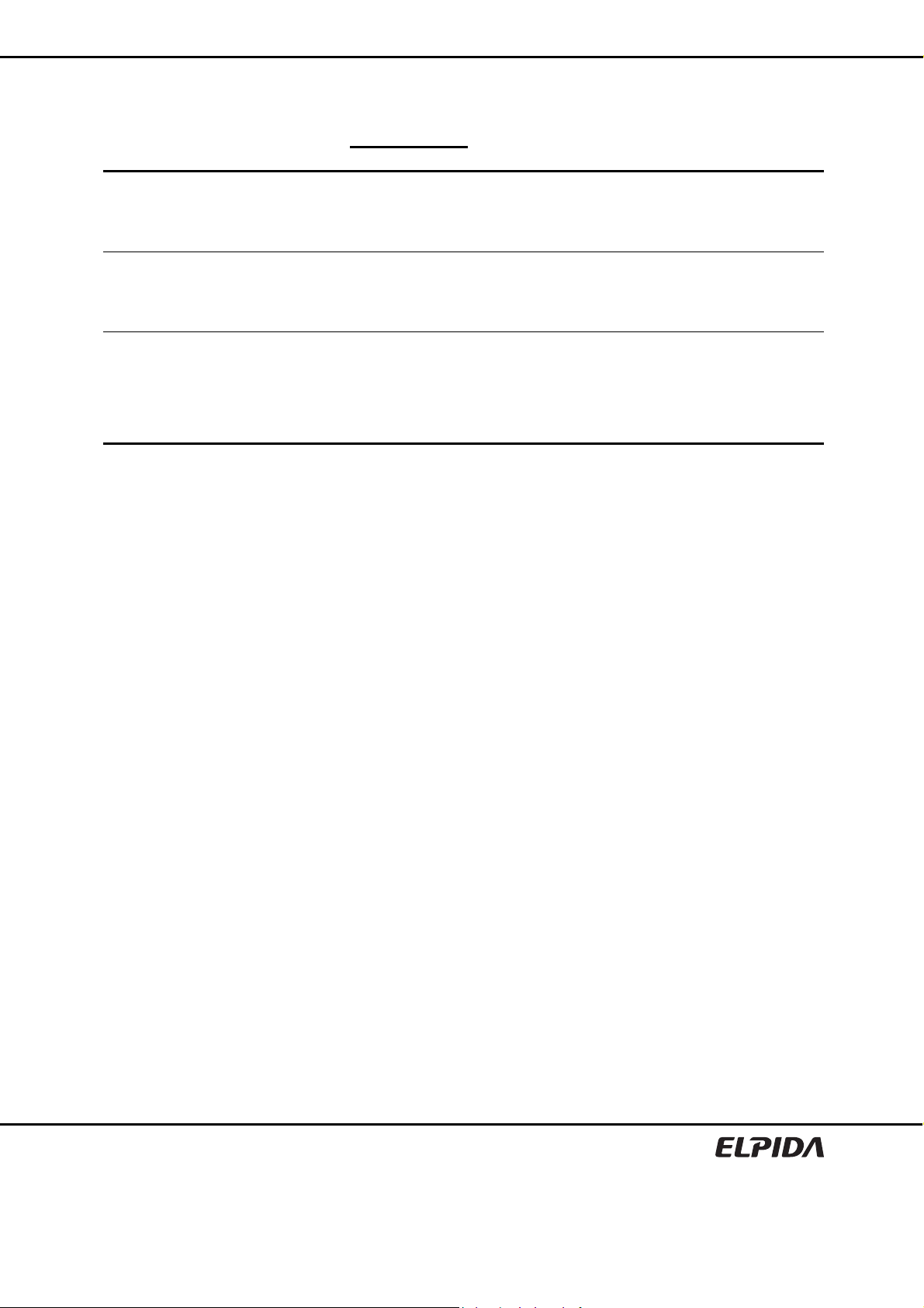
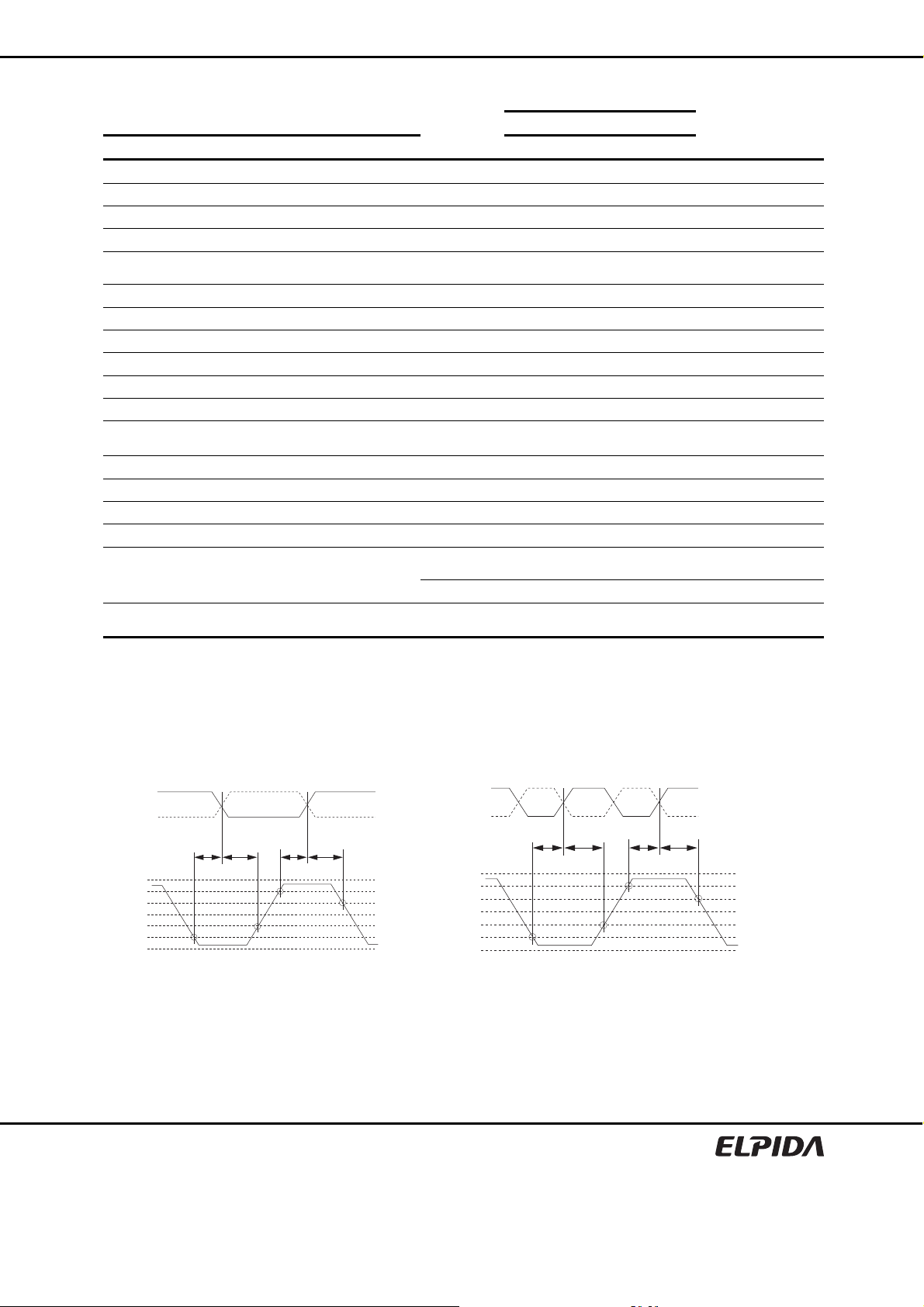
4. The figures of Input Waveform Timing 1 and 2 are referenced from the input signal crossing at the
VIH(AC) level for a rising signal and VIL(AC) for a falling signal applied to the device under test.
5. The figures of Input Waveform Timing 1 and 2 are referenced from the input signal crossing at the
VIL(DC) level for a rising signal and VIH(DC) for a falling signal applied to the device under test.
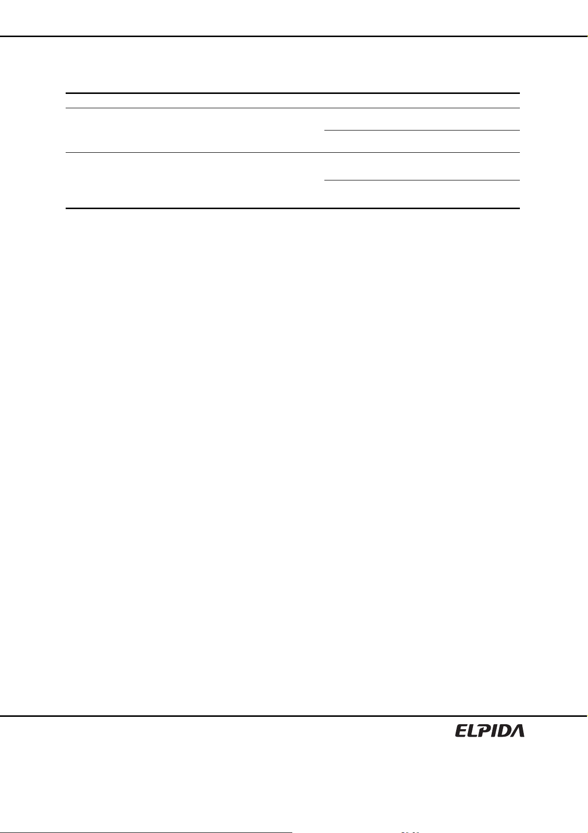
DQS
/DQS
tDS tDH
Input Waveform Timing 1 (tDS, tDH) Input Waveform Timing 2 (tIS, tIH)
Preliminary Data Sheet E1196E10 (Ver. 1.0)
tDS tDH
VDDQ
VIH (AC)(min.)
VIH (DC)(min.)
VREF
VIL (DC)(max.)
VIL (AC)(max.)
VSS
tIS tIH
tIS tIH
VDDQ
VIH (AC)(min.)
VIH (DC)(min.)
VREF
VIL (DC)(max.)
VIL (AC)(max.)
VSS
17
EDE2104ABSE, EDE2108ABSE
6. tHP is the minimum of the absolute half period of the actua l input clock. tHP is an input parameter but not
an input specification parameter. It is used in conjunction with tQHS to derive the DRAM output timing
tQH.
The value to be used for tQH calculation is determined by the following equation;
tHP = min ( tCH(abs), tCL(abs) ),
where,
tCH(abs) is the minimum of the actual instantaneous clock high time;
tCL(abs) is the minimum of the actual instantaneous clock low time;
7. tQHS accounts for:
a. The pulse duration distortion of on-chip clock ci rcuits, which represents ho w well the actual tHP at the
input is transferred to the output; and
b. The worst case push-out of DQS on one transition followed by the worst case pull-i n of DQ on the
next transition, both of which are independent of each other, due to data pin ske w, output pattern effects,
and p-channel to n-channel variation of the output drivers.
8. tQH = tHP – tQHS, where:
tHP is the minimum of the absolute half period of the actual input clock; and tQHS is the specification
value under the max column.
{The less half-pulse width distortion pr esent, the larger the tQH value is; a nd the larger the valid data e ye
will be.}
Examples:
a. If the system provides tHP of 1315ps into a DDR2-667 SDRAM, the DRAM provides tQH of 975ps
(min.)
b. If the system provides tHP of 1420ps into a DDR2-667 SDRAM, the DRAM provides tQH of 1080ps
(min.)
9. RU stands for round up. WR refers to the tWR parameter stored in the MRS.
10. When the device is operated with input clock jitter, this parameter needs to be derated by the actual
tERR(6-10per) of the input clock. (output deratings are relative to the SDRAM input clock.)
For example, if the measured jitter into a DDR2-667 SDRAM has tERR(6-10per) min. = −272ps and
tERR(6-10per) max. = +293ps, then tDQSCK min.(derated) = tDQSCK min. − tERR(6-10per) max. =
−400ps − 293ps = −693ps and tDQSCK max.(derated) = tDQSCK max. − tERR(6-10per) min. = 400ps +
272ps = +672ps. Similarly, tLZ(DQ) for DDR2-667 derates to tLZ(DQ) min.(derated) = −900ps − 293ps =
−1193ps and tLZ(DQ) max.(derated)= 450ps + 272ps = +722ps.
11. When the device is operated with input clock jitter, this parameter needs to be derated by the actual
tJIT(per) of the input clock. (output deratings are relative to the SDRAM input clock.)
For example, if the measured jitter into a DDR2-667 SDRAM has tJIT(per) min. = −72ps and
tJIT(per) max. = +93ps, then tRPRE min.(derated) = tRPRE min. + tJIT(per) min. = 0.9 × tCK(avg) − 72ps
= +2178ps and tRPRE max.(derated) = tRPRE max. + tJIT(per) max. = 1.1 × tCK(avg) + 93ps = +2843ps.
12. When the device is operated with input clock jitter, this parameter needs to be derated by the actual
tJIT(duty) of the input clock. (output deratings are relative to the SDRAM input clock.)
For example, if the measured jitter into a DDR2-667 SDRAM has tJIT(duty) min. = −72ps and
tJIT(duty) max. = +93ps, then tRPST min.(derated) = tRPST min. + tJIT(duty) min. = 0.4 × tCK(avg) −
72ps = +928ps and tRPST max.(derated) = tRPST max. + tJIT(duty) max. = 0.6 × tCK(avg) + 93ps =
+1592ps.
13. Refer to the Clock Jitter table.
Preliminary Data Sheet E1196E10 (Ver. 1.0)
18
EDE2104ABSE, EDE2108ABSE
ODT AC Electrical Characteristics
Parameter Symbol min. max. Unit Notes
ODT turn-on delay tAOND 2 2 tCK
ODT turn-on
-8G, -6E
-5C tAON tAC (min) tAC (max) + 1000 ps 1
ODT turn-on (power-down mode) tAONPD tAC(min) + 2000 2tCK + tAC(max) + 1000 ps
ODT turn-off delay tAOFD 2.5 2.5 tCK 5, 6
ODT turn-off tAOF tAC(min) tAC(max) + 600 ps 2, 4, 5, 6
ODT turn-off (power-down mode) tAOFPD tAC(min) + 2000 2.5tCK + tAC(max) + 1000 ps
ODT to power-down entry latency tANPD 3 3 tCK
ODT power-down exit latency tAXPD 8 8 tCK
Notes: 1. ODT turn on time min is when the device leaves high impedance and ODT resistance begins to turn on.
ODT turn on time max is when the ODT resistance is fully on. Both are measured from tAOND.
2. ODT turn off time min is when the device starts to turn off ODT resistance.
ODT turn off time max is when the bus is in high impedance. Both are measured from tAOFD.
3. When the device is operated with input clock jitter, this parameter needs to be derated by the actual
tERR(6-10per) of the input clock. (output deratings are relative to the SDRAM input clock.)
4. When the device is operated with input clock jitter, this parameter needs to be derated by
{−tJIT(duty) max. − tERR(6-10per) max. } and { −tJIT(duty) min. − tERR(6-10per) min. } of the actual input
clock.(output deratings are relative to the SDRAM input clock.)
For example, if the measured jitter into a DDR2-667 SDRAM has tERR(6-10per) min. = −272ps,
tERR(6-10per) max. = +293ps, tJIT(duty) min. = −106ps and tJIT(duty) max. = +94ps, then
tAOF min.(derated) = tAOF min. + { −tJIT(duty) max. − tERR(6-10per) max. } = −450ps + { −94ps − 293ps}
= −837ps and tAOF max.(derated) = tAOF max. + { −tJIT(duty) min. − tERR(6-10per) min. } = 1050ps +
{ 106ps + 272ps} = +1428ps.
5. For tAOFD of DDR2-533, the 1/2 clock of tCK in the 2.5 × tCK assumes a tCH, input clock high pulse
width of 0.5 relative to tCK. tAOF min. and tAOF max. should each be derated by t he same amount as
the actual amount of tCH offset present at the DRAM input with respect to 0.5. For example, if an input
clock has a worst case tCH of 0.45, the tAOF min. should be derated by subtracting 0.05 × tCK from it,
whereas if an input clock has a worst case tCH of 0.55, the tAOF max. should be derated by adding 0.05
× tCK to it. Therefore, we have;
tAOF min.(derated) = tAC min. − [0.5 − Min.(0.5, tCH min.)] × tCK
tAOF max.(derated) = tAC max. + 0.6 + [Max.(0.5, tCH max.) − 0.5] × tCK
or
tAOF min.(derated) = Min.(tAC min., tAC min. − [0.5 − tCH min.] × tCK)
tAOF max.(derated) = 0.6 + Max.(tAC max., tAC max. + [tCH max. − 0.5] × tCK)
where tCH min. and tCH max. are the m inimum and maximum of tCH actually measured at the DRAM
input balls.
6. For tAOFD of DDR2-667/800, the 1/2 clock of nCK in the 2.5 ×
clock high pulse width of 0.5 relative to tCK(avg). tAOF min. and tAOF max. should each be d erated by
the same amount as the actual amount of tCH(avg) offset present at the DRAM input with respect to 0.5.
For example, if an input clock has a worst case tCH(avg) of 0.48, the tAOF min. should be derated by
subtracting 0.02 × tCK(avg) from it, whereas if an input clock has a worst case tCH(avg) of 0.52,
the tAOF max. should be derated by adding 0.02 × tCK(avg) to it. Therefore, we have;
tAOF min.(derated) = tAC min. − [0.5 − Min.(0.5, tCH(avg) min.)] × tCK(avg)
tAOF max.(derated) = tAC max. + 0.6 + [Max.(0.5, tCH(avg) max.) − 0.5] × tCK(avg)
or
tAOF min.(derated) = Min.(tAC min., tAC min. − [0.5 − tCH(avg) min.] × tCK(avg))
tAOF max.(derated) = 0.6 + Max.(tAC max., tAC max. + [tCH(avg) max. − 0.5] × tCK(avg))
where tCH(avg) min. and tCH(avg) max. are the minimum and ma ximum of tCH(avg) actually measured
at the DRAM input balls.
tAON tAC (min) tAC (max) + 700 ps 1, 3
nCK assumes a tCH(avg), average input
Preliminary Data Sheet E1196E10 (Ver. 1.0)
19
EDE2104ABSE, EDE2108ABSE
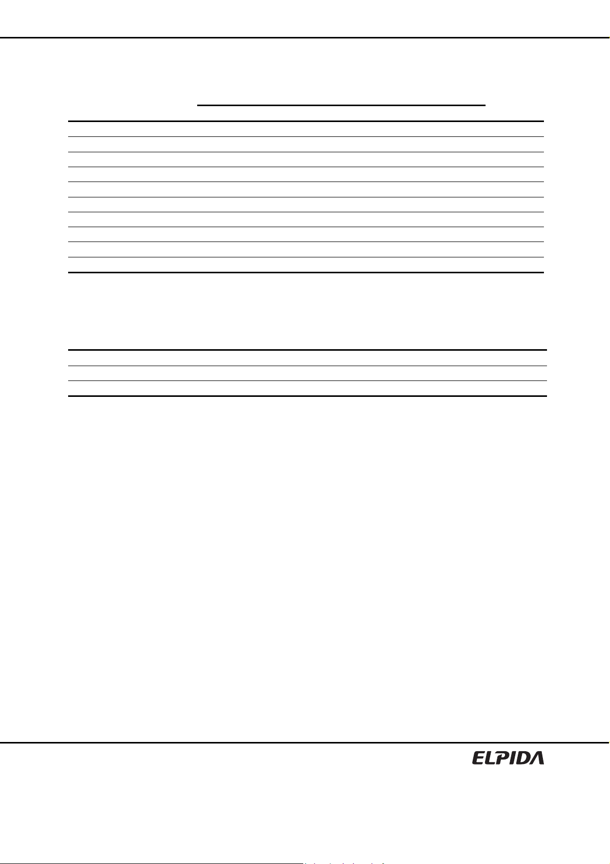
AC Input Test Conditions
Parameter Symbol Value Unit Notes
Input reference voltage VREF 0.5 × VDDQ V 1
Input signal maximum peak to peak swing VSWING (max.) 1.0 V 1
Input signal minimum slew rate SLEW 1.0 V/ns 2, 3
Notes: 1. Input waveform timing is referenced to the input signal crossing through the VIH/IL (AC) level applied to
the device under test.
2. The input signal minimum sle w rate is to be maintained over the range from VREF to VIH (AC) min. for
rising edges and the range from VREF to VIL (AC) max. for falling edges as shown in the below figure.
3. AC timings are referenced with input waveforms switching from VIL (AC) to VIH (AC) on the positive
transitions and VIH (AC) to VIL (AC) on the negative transitions.
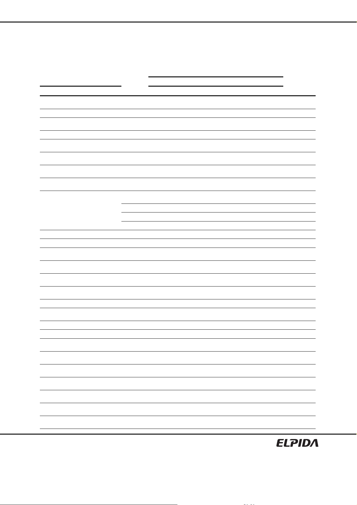
VDDQ
VIH (AC)(min.)
VIH (DC)(min.)
VSWING(max.)
VREF
VIL (DC)(max.)
VIL (AC)(max.)
Falling slew =
ΔTF
VREF
ΔTR
−
VIL (AC)(max.)
ΔTF
Rising slew =
AC Input Test Signal Wave forms
Measurement point
DQ
RT =25 Ω
Output Load
VTT
VIH (AC) min. − VREF
VSS
ΔTR
Preliminary Data Sheet E1196E10 (Ver. 1.0)
20
EDE2104ABSE, EDE2108ABSE
Clock Jitter [DDR2-800, 667]
-8G -6E
Frequency (Mbps) 800 667
Parameter Symbol min. max. min. max. Unit Notes
Average clock period tCK (avg) 2500 8000 3000 8000 ps 1
Clock period jitter tJIT (per) −100 100 −125 125 ps 5
Clock period jitter during
DLL locking period
Cycle to cycle period jitter tJIT (cc) ⎯ 200 ⎯ 250 ps 6
Cycle to cycle clock period jitter
during DLL locking period
Cumulative error across 2 cycles tERR (2per) −150 150 −175 175 ps 7
Cumulative error across 3 cycles tERR (3per) −175 175 −225 225 ps 7
Cumulative error across 4 cycles tERR (4per) −200 200 −250 250 ps 7
Cumulative error across 5 cycles tERR (5per) −200 200 −250 250 ps 7
Cumulative error across
n=6,7,8,9,10 cycles
Cumulative error across
n=11, 12,…49,50 cycles
Average high pulse width tCH (avg) 0.48 0.52 0.48 0.52 tCK (avg) 2
Average low pulse width tCL (avg) 0.48 0.52 0.48 0.52 tCK (avg) 3
Duty cycle jitter tJIT (duty) −100 100 −125 125 ps 4
Notes: 1. tCK (avg) is calculated as the average clock period across any consecutive 200cycle window.
tJIT
(per, lck)
tJIT (cc, lck) ⎯ 160 ⎯ 200 ps 6
tERR
(6-10per)
tERR
(11-50per)
−80 80 −100 100 ps 5
−300 300 −350 350 ps 7
−450 450 −450 450 ps 7
N
⎧
=
)(
⎨
∑
=1
j
⎩
N = 200
2. tCH (avg) is defined as the average high pulse width, as calculated across any consecutive 200 high
pulses.
N
⎧
=
⎨
∑
j
=
⎩
3. tCL (avg) is defined as the average low pulse width, as calculated across a ny consecutive 200 low pulses.
N
⎧
=
⎨
∑
j
=
⎩
4. tJIT (duty) is defined as the cumulative set of tCH jitter and tCL jitter. tCH jitter is the largest deviation of
any single tCH from tCH (avg). tCL jitter is the largest deviation of any single tCL from tCL (avg).
tJIT (duty) is not subject to production test.
tJIT (duty) = Min./Max. of {tJIT (CH), tJIT (CL)}, where:
tJIT (CH) = {tCH
tJIT (CL) = {tCL
5. tJIT (per) is defined as the largest deviation of any single tCK from tCK (avg).
tJIT (per) = Min./Max. of { tCK
tJIT (per) defines the single period jitter when the DLL is already locked. tJIT (per, lck) uses the same
definition for single period jitter, during the DLL locking period only. tJIT (per) and tJIT (per, lck) are not
subject to production test.
- tCH (avg) where j = 1 to 200}
j
− tCL (avg) where j = 1 to 200}
j
− tCK (avg) where j = 1 to 200}
j
1
N = 200
1
N = 200
⎫
⎬
⎭
⎫
⎬
⎭
⎫
NtCKjavgtCK
⎬
⎭
))(()(
×
×
avgtCKNtCHjavgtCH
))(()(
avgtCKNtCLjavgtCL
Preliminary Data Sheet E1196E10 (Ver. 1.0)
21
EDE2104ABSE, EDE2108ABSE
6. tJIT (cc) is defined as the absolute difference in clock period between two consec utive clock cycles:
tJIT (cc) = Max. of |tCK
tJIT (cc) is defines the cycle to cycle jitter when the DLL is already locked. tJIT (cc, lck) uses the same
definition for cycle to cycle jitter, during the DLL locking period only. tJIT (cc) and tJIT (cc, lck) are not
subject to production test.
7. tERR (nper) is defined as the cumulative error across multiple consecutive cycles from tCK (avg).
tERR (nper) is not subject to production test.
8. These parameters are specified per their average values, however it is understood that the following
relationship between the average timing and the absolute instantaneous timing hold at all times.
(minimum and maximum of spec values are to be used for calculations in the table below.)
Parameter Symbol min. max. Unit
Absolute clock period tCK (abs) tCK (avg) min. + tJIT (per) min. tCK (avg) max. + tJIT (per) max. ps
Absolute clock high pulse
width
Absolute clock low pulse
width
Example: For DDR2-667, tCH(abs) min. = ( 0.48 × 3000 ps ) - 125ps = 1315ps
− tCKj|
j+1
tCH (abs)
tCL (abs)
n
⎧
=
⎨
∑
=
j
⎩
2 ≤ n ≤ 50 for tERR (nper)
tCH (avg) min. × tCK (avg) min. +
tJIT (duty) min.
tCL (avg) min. × tCK (avg) min. +
tJIT (duty) min.
⎫
×−
⎬
1
⎭
))()(
avgtCKntCKjnpertERR
tCH (avg) max. × tCK (avg) max.
+ tJIT (duty) max.
tCL (avg) max. × tCK (avg) max.
+ tJIT (duty) max.
ps
ps
Preliminary Data Sheet E1196E10 (Ver. 1.0)
22
EDE2104ABSE, EDE2108ABSE
Input Slew Rate Derating
For all input signals the total tIS, tDS (setup time) and tIH, tDH (hold time) required is calculated by adding the data
sheet tIS (base), tDS (base) and tIH (base), tDH (base) value to the ΔtIS, ΔtDS and ΔtIH, ΔtDH derating value
respectively.
Example: tDS (total setup time) = tDS (base) + ΔtDS.
Setup (tIS, tDS) nominal slew rate for a rising signal is defined as the slew rate bet ween the last crossing of VREF
(DC) and the first crossing of VIH (AC) min. Setup (tIS, tDS) nominal slew rate for a falling signal is defined as the
slew rate between the last crossing of VREF (DC) and the first crossing of VIL (AC) max. If the actual signal is
always earlier than the nominal slew rate line between shaded ‘VREF (DC) to AC region’, use nominal slew rate for
derating value (See the figure of Slew Rate Definition Nominal).
If the actual signal is later than the nominal slew rate line anywhere between shaded ‘VREF (DC) to AC region’, the
slew rate of a tangent line to the actual signal from the AC level to DC level is used for derating value (see the figure
of Slew Rate Definition Tangent).
Hold (tIH, tDH) nominal slew rate for a rising signal is defined as the slew rate between the last crossing of
VIL (DC) max. and the first crossing of VREF (DC). Hold (tIH, tDH) nominal slew rate for a falling signal is defined
as the slew rate between the last crossing of VIH (DC) min. and the first crossing of VRE F (DC). If the actual signal
is always later than the nominal slew rate line between shaded ‘DC lev el to VREF (DC) region’, use nominal slew
rate for derating value (See the figure of Slew Rate Definition Nominal).
If the actual signal is earlier than the nominal slew rate line anywhere between shaded ‘DC to VREF (DC) region’,
the slew rate of a tangent line to the actual signal from the DC level to VREF (DC) level is used for derating value
(see the figure of Slew Rate Definition Tangent).
Although for slow slew rates the total setup time might be negative (i.e. a valid i nput signal will not have reached
VIH/IL (AC) at the time of the rising clock transition) a valid input signal is still required to complete the transition and
reach VIH/IL (AC).
For slew rates in between the values listed in the tables below, the derating values may obtained by linear
interpolation.
These values are typically not subject to production test. They are verified by design and characterization.
[Derating Values of tDS/tDH with Differential DQS (DDR2-533)]
DQS, /DQS differential slew rate
4.0 V/ns 3.0 V/ns 2.0 V/ns 1.8 V/ns 1.6 V/ns 1.4 V/ns 1.2 V/ns 1.0 V/ns 0.8 V/ns
ΔtDS ΔtDH ΔtDS ΔtDH ΔtDS ΔtDH ΔtDS ΔtDH ΔtDS ΔtDH ΔtDS ΔtDH ΔtDS ΔtDH ΔtDS ΔtDH ΔtDS ΔtDH Unit
2.0 +125 +45 +125 +45 +125 +45 ⎯ ⎯ ⎯ ⎯ ⎯ ⎯ ⎯ ⎯ ⎯ ⎯ ⎯ ⎯ ps
1.5 +83 +21 +83 +21 +83 +21 +95 +33 ⎯ ⎯ ⎯ ⎯ ⎯ ⎯ ⎯ ⎯ ⎯ ⎯ ps
1.0 0 0 0 0 0 0 +12 +12 +24 +24 ⎯ ⎯ ⎯ ⎯ ⎯ ⎯ ⎯ ⎯ ps
DQ
slew
rate
(V/ns)
0.9 ⎯ ⎯ −11 −14 −11 −14 +1 −2 +13 +10 +25 +22 ⎯ ⎯ ⎯ ⎯ ⎯ ⎯ ps
0.8 ⎯ ⎯ ⎯ ⎯ −25 −31 −13 −19 −1 −7 11 +5 +23 +17 ⎯ ⎯ ⎯ ⎯ ps
0.7 ⎯ ⎯ ⎯ ⎯ ⎯ ⎯ −31 −42 −19 −30 −7 −18 +5 −6 +17 +6 ⎯ ⎯ ps
0.6 ⎯ ⎯ ⎯ ⎯ ⎯ ⎯ ⎯ ⎯ −43 −59 −31 −47 −19 −35 −7 −23 +5 −11 ps
0.5 ⎯ ⎯ ⎯ ⎯ ⎯ ⎯ ⎯ ⎯ ⎯ ⎯ −74 −89 −62 −77 −50 −65 −38 −53 ps
0.4 ⎯ ⎯ ⎯ ⎯ ⎯ ⎯ ⎯ ⎯ ⎯ ⎯ ⎯ ⎯ −127 −140 −115 −128 −103 −116 ps
Preliminary Data Sheet E1196E10 (Ver. 1.0)
23
EDE2104ABSE, EDE2108ABSE
[Derating Values of tDS/tDH with Differential DQS (DDR2-667, 800)
DQS, /DQS differential slew rate
4.0 V/ns 3.0 V/ns 2.0 V/ns 1.8 V/ns 1.6 V/ns 1.4 V/ns 1.2 V/ns 1.0 V/ns 0.8 V/ns
ΔtDS ΔtDH ΔtDS ΔtDH ΔtDS ΔtDH ΔtDS ΔtDH ΔtDS ΔtDH ΔtDS ΔtDH ΔtDS ΔtDH ΔtDS ΔtDH ΔtDS ΔtDH Unit
2.0 +100 +45 +100 +45 +100 +45 ⎯ ⎯ ⎯ ⎯ ⎯ ⎯ ⎯ ⎯ ⎯ ⎯ ⎯ ⎯ ps
1.5 +67 +21 +67 +21 +67 +21 +79 +33 ⎯ ⎯ ⎯ ⎯ ⎯ ⎯ ⎯ ⎯ ⎯ ⎯ ps
1.0 0 0 0 0 0 0 +12 +12 +24 +24 ⎯ ⎯ ⎯ ⎯ ⎯ ⎯ ⎯ ⎯ ps
DQ
slew
rate
(V/ns)
0.9 ⎯ ⎯ −5 −14 −5 −14 +7 −2 +19 +10 +31 +22 ⎯ ⎯ ⎯ ⎯ ⎯ ⎯ ps
0.8 ⎯ ⎯ ⎯ ⎯ −13 −31 −1 −19 +11 −7 +23 +5 +35 +17 ⎯ ⎯ ⎯ ⎯ ps
0.7 ⎯ ⎯ ⎯ ⎯ ⎯ ⎯ −10 −42 +2 −30 +14 −18 +26 −6 +38 +6 ⎯ ⎯ ps
0.6 ⎯ ⎯ ⎯ ⎯ ⎯ ⎯ ⎯ ⎯ −10 −59 +2 −47 +14 −35 +26 −23 +38 −11 ps
0.5 ⎯ ⎯ ⎯ ⎯ ⎯ ⎯ ⎯ ⎯ ⎯ ⎯ −24 −89 −12 −77 0 −65 +12 −53 ps
0.4 ⎯ ⎯ ⎯ ⎯ ⎯ ⎯ ⎯ ⎯ ⎯ ⎯ ⎯ ⎯ −52 −140 −40 −128 −28 −116 ps
[Derating Values of tDS1/tDH1 with Single-Ended DQS (DDR2-533)]
DQS, /DQS single-ended slew rate
2.0 V/ns 1.5 V/ns 1.0V/ns 0.9V/ns 0.8V/ns 0.7 V/ns 0.6 V/ns 0.5 V/ns 0.4 V/ns
DQ
slew
rate
(V/ns)
Δ
tDS1 Δ tDH1 Δ tDS1Δ tDH1 Δ tDS1 Δ tDH1Δ tDS1Δ tDH1Δ tDS1Δ tDH1Δ tDS1Δ tDH1Δ tDS1Δ tDH1 Δ tDS1 Δ tDH1 Δ tDS1 Δ tDH1
2.0 +188 +188 +167 +146 +125 +63 ⎯ ⎯ ⎯ ⎯ ⎯ ⎯ ⎯ ⎯ ⎯ ⎯ ⎯ ⎯ ps
1.5 +146 +167 +125 +125 +83 +42 +81 +43 ⎯ ⎯ ⎯ ⎯ ⎯ ⎯ ⎯ ⎯ ⎯ ⎯ ps
1.0 +63 +125 +42 +83 0 0 −2 +1 −7 −13 ⎯ ⎯ ⎯ ⎯ ⎯ ⎯ ⎯ ⎯ ps
0.9 ⎯ ⎯ +31 +69 −11 −14 −13 −13 −18 −27 −29 −45 ⎯ ⎯ ⎯ ⎯ ⎯ ⎯ ps
0.8 ⎯ ⎯ ⎯ ⎯ −25 −31 −27 −30 −32 −44 −43 −62 −60 −86 ⎯ ⎯ ⎯ ⎯ ps
0.7 ⎯ ⎯ ⎯ ⎯ ⎯ ⎯ −45 −53 −50 −67 −61 −85 −78 −109 −108 −152 ⎯ ⎯ ps
0.6 ⎯ ⎯ ⎯ ⎯ ⎯ ⎯ ⎯ ⎯ −74 −96 −85 −114 −102 −138 −132 −181 −183 −246 ps
0.5 ⎯ ⎯ ⎯ ⎯ ⎯ ⎯ ⎯ ⎯ ⎯ ⎯ −128 −156 −145 −180 −175 −223 −226 −288 ps
0.4 ⎯ ⎯ ⎯ ⎯ ⎯ ⎯ ⎯ ⎯ ⎯ ⎯ ⎯ ⎯ −210 −243 −240 −286 −291 −351 ps
Unit
Preliminary Data Sheet E1196E10 (Ver. 1.0)
24
EDE2104ABSE, EDE2108ABSE
[Derating Values of tIS/tIH (DDR2-533)]
CK, /CK Differential Slew Rate
2.0 V/ns 1.5 V/ns 1.0 V/ns
ΔtIS ΔtIH ΔtIS ΔtIH ΔtIS ΔtIH Unit Notes
4.0 +187 +94 +217 +124 +247 +154 ps
3.5 +179 +89 +209 +119 +239 +149 ps
3.0 +167 +83 +197 +113 +227 +143 ps
2.5 +150 +75 +180 +105 +210 +135 ps
2.0 +125 +45 +155 +75 +185 +105 ps
1.5 +83 +21 +113 +51 +143 +81 ps
1.0 0 0 +30 +30 +60 60 ps
0.9 −11 −14 +19 +16 +49 +46 ps
Command/address
slew rate (V/ns)
0.8 −25 −31 +5 −1 +35 +29 ps
0.7 −43 −54 −13 −24 +17 +6 ps
0.6 −67 −83 −37 −53 −7 −23 ps
0.5 −110 −125 −80 −95 −50 −65 ps
0.4 −175 −188 −145 −158 −115 −128 ps
0.3 −285 −292 −255 −262 −225 −232 ps
0.25 −350 −375 −320 −345 −290 −315 ps
0.2 −525 −500 −495 −470 −465 −440 ps
0.15 −800 −708 −770 −678 −740 −648 ps
0.1 −1450 −1125 −1420 −1095 −1390 −1065 ps
Preliminary Data Sheet E1196E10 (Ver. 1.0)
25
 Loading...