


PRELIMINARY DATA SHEET
2G bits DDR2 SDRAM
EDE2104ABSE (512M words × 4 bits)
EDE2108ABSE (256M words × 8 bits)
Specifications
• Density: 2G bits
• Organization
⎯ 64M words × 4 bits × 8 banks (EDE2104ABSE)
⎯ 32M words × 8 bits × 8 banks (EDE2108ABSE)
• Package
⎯ 68-ball FBGA
⎯ Lead-free (RoHS compliant)
• Power supply: VDD, VDDQ = 1.8V ± 0.1V
• Data rate
⎯ 800Mbps/667Mbps/533Mbps (max.)
• 1KB page size
⎯ Row address: A0 to A14
⎯ Column address: A0 to A9, A11 (EDE2104ABSE)
A0 to A9 (EDE2108ABSE)
• Eight internal banks for concurrent operation
• Interface: SSTL_18
• Burst lengths (BL): 4, 8
• Burst type (BT):
⎯ Sequential (4, 8)
⎯ Interleave (4, 8)
• /CAS Latency (CL): 3, 4, 5, 6
• Precharge: auto precharge option for each burst
access
• Driver strength: normal/weak
• Refresh: auto-refresh, self-refresh
• Refresh cycles: 8192 cycles/64ms
⎯ Average refresh period
7.8μs at 0°C ≤ TC ≤ +85°C
3.9μs at +85°C < TC ≤ +95°C
• Operating case temperature range
⎯ TC = 0°C to +95°C
Features
• Double-data-rate architecture; two data transfers per
clock cycle
• The high-speed data transfer is realized by the 4 bits
prefetch pipelined architecture
• Bi-directional differential data strobe (DQS and /DQS)
is transmitted/received with data for capturing data at
the receiver
• DQS is edge-aligned with data for READs; centeraligned with data for WRITEs
• Differential clock inputs (CK and /CK)
• DLL aligns DQ and DQS transitions with CK
transitions
• Commands entered on each positive CK edge; data
and data mask referenced to both edges of DQS
• Data mask (DM) for write data
• Posted /CAS by programmable additive latency for
better command and data bus efficiency
• Off-Chip-Driver Impedance Adjustment and On-DieTermination for better signal quality
• Programmable RDQS, /RDQS output for making × 8
organization compatible to × 4 organization
• /DQS, (/RDQS) can be disabled for single-ended
Data Strobe operation
Document No. E1196E10 (Ver. 1.0)
Date Published November 2007 (K) Japan
Printed in Japan
URL: http://www.elpida.com
©Elpida Memory, Inc. 2007
Ordering Information
Part number
EDE2104ABSE-8G-E
EDE2104ABSE-6E-E
EDE2104ABSE-5C-E
EDE2108ABSE-8G-E
EDE2108ABSE-6E-E
EDE2108ABSE-5C-E
Part Number
Elpida Memory
Type
D: Monolithic Device
Product Family
E: DDR2
Density / Bank
21: 2Gb / 8-bank
Organization
04: x4
08: x8
Power Supply, Interface
A: 1.8V, SSTL_18
Mask
version
B 512M × 4 8
256M × 8
EDE2104ABSE, EDE2108ABSE
Organization
(words × bits)
Internal
Banks
Speed bin
(CL-tRCD-tRP)
DDR2-800 (6-6-6)
DDR2-667 (5-5-5)
DDR2-533 (4-4-4)
DDR2-800 (6-6-6)
DDR2-667 (5-5-5)
DDR2-533 (4-4-4)
E D E 21 04 A B SE - 8G - E
Speed
8G DDR2-800 (6-6-6)
6E: DDR2-667 (5-5-5)
5C: DDR2-533 (4-4-4)
Package
SE: FBGA
Die Rev.
Package
68-ball FBGA
Environment code
E: Lead Free
(RoHS compliant)
Preliminary Data Sheet E1196E10 (Ver. 1.0)
2
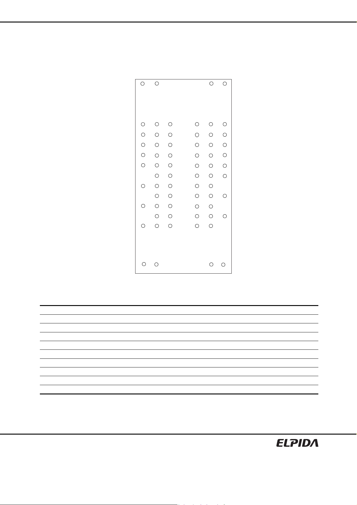
Pin Configurations
/xxx indicates active low signal.
EDE2104ABSE, EDE2108ABSE
68-ball FBGA
(×8, ×4 organization)
2
1
A
NC
B
C
D
3
7
8
9
NC
NCNC
E
F
G
H
J
K
L
M
N
P
R
T
U
V
W
Note: ( )* marked pins are for ×4 organization.
VDD
DQ6
(NC)*
VDDQ
DQ4
(NC)*
VDDL
BA2
VSS
VDD
NC
NU/ /RDQS
VSS
(NC)*
DM/RDQS
VSSQ
(DM)*
DQ1
VDDQ
VSSQ
DQ3
VREF
VSS
CKE
/WE
BA0
BA1
A10
A1
A3
A5
A7
A9
A12
A14
NC NC NC
(Top view)
VSSQ
DQS
VDDQ
DQ2
VSSDL
/RAS
/CAS
A2
A6
A11
NC
/DQS
VSSQ
DQ0
VSSQ
CK
/CK
/CS
A0
A4
A8
A13
VDDQ
DQ7
(NC)*
VDDQ
DQ5
(NC)*
VDD
ODT
VDD
VSS
Pin name Function Pin name Function
A0 to A14 Address inputs ODT ODT control
BA0, BA1, BA2 Bank select VDD Supply voltage for internal circuit
DQ0 to DQ7 Data input/output VSS Ground for internal circuit
DQS, /DQS Differential data strobe VDDQ Supply voltage for DQ circuit
RDQS, /RDQS Differential data strobe for read VSSQ Ground for DQ circuit
/CS Chip select VREF Input reference voltage
/RAS, /CAS, /WE Command input VDDL Supply voltage for DLL circuit
CKE Clock enable VSSDL Ground for DLL circuit
CK, /CK Differential clock input NC*1 No connection
DM Write data mask NU*2 Not usable
Notes: 1. Not internally connected with die.
2. Don’t connect. Internally connected.
Preliminary Data Sheet E1196E10 (Ver. 1.0)
3

CONTENTS
EDE2104ABSE, EDE2108ABSE
Specifications.................................................................................................................................................1
Features.........................................................................................................................................................1
Ordering Information......................................................................................................................................2
Part Number ..................................................................................................................................................2
Pin Configurations.........................................................................................................................................3
Electrical Specifications.................................................................................................................................5
Block Diagram .............................................................................................................................................29
Pin Function.................................................................................................................................................30
Command Operation...................................................................................................................................32
Simplified State Diagram.............................................................................................................................40
Operation of DDR2 SDRAM........................................................................................................................41
Package Drawing ........................................................................................................................................78
Recommended Soldering Conditions..........................................................................................................79
Preliminary Data Sheet E1196E10 (Ver. 1.0)
4
EDE2104ABSE, EDE2108ABSE
Electrical Specifications
• All voltages are referenced to VSS (GND)
• Execute power-up and Initialization sequence before proper device oper ation is achieved.
Absolute Maximum Ratings
Parameter Symbol Rating Unit Notes
Power supply voltage VDD −1.0 to +2.3 V 1
Power supply voltage for output VDDQ −0.5 to +2.3 V 1
Input voltage VIN −0.5 to +2.3 V 1
Output voltage VOUT −0.5 to +2.3 V 1
Storage temperature Tstg −55 to +100 °C 1, 2
Power dissipation PD 1.0 W 1
Short circuit output current IOUT 50 mA 1
Notes: 1. Stresses greater than those listed under Absolute Maximum Ratings may cause permanent damage to
the device. This is a stress rating only and functional operation of the device at these or any other
conditions above those indicated in the operational sections of this spec ification is not implied. E xposure
to absolute maximum rating conditions for extended periods may affect reliability.
2. Storage temperature is the case surface temperature on the center/top side of the DRAM.
Caution
Exposing the device to stress above those listed in Absolute Maximum Ratings could cause
permanent damage. The device is not meant to be operated under conditions outside the limits
described in the operational section of this specification. Exposure to Absolute Maximum Rating
conditions for extended periods may affect device reliability.
Operating Temperature Condition
Parameter Symbol Rating Unit Notes
Operating case temperature TC 0 to +95 °C 1, 2
Notes: 1. Operating temperature is the case surface temperature on the center/top side of the DRAM.
2. Supporting 0°C to +85°C with full AC and DC specifications.
Supporting 0°C to +85°C and being able to extend to +95°C with doubling auto-refresh commands in
frequency to a 32ms period (tREFI = 3.9µs) and higher temperature Self-Refresh entry via A7 "1" on
EMRS (2).
Preliminary Data Sheet E1196E10 (Ver. 1.0)
5
EDE2104ABSE, EDE2108ABSE
Recommended DC Operating Conditions (SSTL_18)
Parameter Symbol min. typ. max. Unit Notes
Supply voltage VDD 1.7 1.8 1.9 V 4
Supply voltage for output VDDQ 1.7 1.8 1.9 V 4
Input reference voltage VREF 0.49 × VDDQ 0.50 × VDDQ 0.51 × VDDQ V 1, 2
Termination voltage VTT VREF − 0.04 VREF VREF + 0.04 V 3
DC input logic high VIH (DC) VREF + 0.125 ⎯ VDDQ + 0.3 V
DC input low VIL (DC) −0.3 ⎯ VREF – 0.125 V
AC input logic high
-8G, -6E
-5C VIH (AC) VREF + 0.250 ⎯ ⎯ V
AC input low
-8G, -6E
-5C VIL (AC) ⎯ ⎯ VREF − 0.250 V
Notes: 1. The value of VREF may be selected by the user to provide optimum noise margin in the system. Typically
the value of VREF is expected to be about 0.5 × VDDQ of the transmitting device and VREF are expected
to track variations in VDDQ.
2. Peak to peak AC noise on VREF may not exceed ±2% VREF (DC).
3. VTT of transmitting device must track VREF of receiving device.
4. VDDQ tracks with VDD, VDDL tracks with VDD. AC parameters are measured with VDD, VDDQ and
VDDL tied together.
VIH (AC) VREF + 0.200 ⎯ ⎯ V
VIL (AC) ⎯ ⎯ VREF – 0.200 V
Preliminary Data Sheet E1196E10 (Ver. 1.0)
6
EDE2104ABSE, EDE2108ABSE
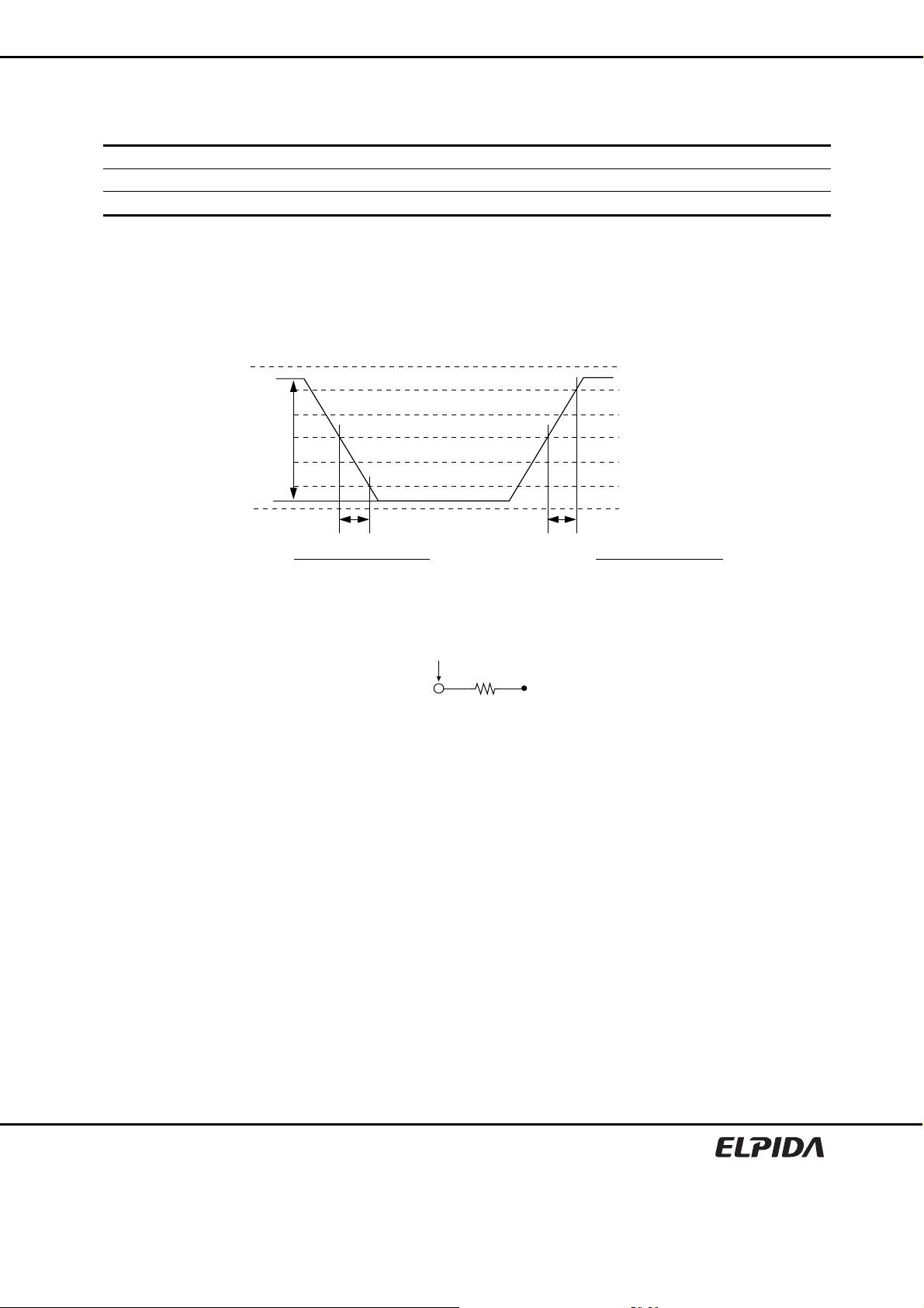
AC Overshoot/Undershoot Specification
Parameter Pins Specification Unit
Maximum peak amplitude allowed for overshoot
Maximum peak amplitude allowed for undershoot 0.5 V
Maximum overshoot area above VDD
DDR2-800
DDR2-667 0.8 V-ns
DDR2-533 1.0 V-ns
Maximum undershoot area below VSS
DDR2-800
DDR2-667 0.8 V-ns
DDR2-533 1.0 V-ns
Maximum peak amplitude allowed for overshoot CK, /CK 0.5 V
Maximum peak amplitude allowed for undershoot 0.5 V
Maximum overshoot area above VDD
DDR2-800, 667
DDR2-533 0.28 V-ns
Maximum undershoot area below VSS
DDR2-800, 667
DDR2-533 0.28 V-ns
Maximum peak amplitude allowed for overshoot DQ, DQS, /DQS, 0.5 V
Maximum peak amplitude allowed for undershoot RDQS, /RDQS, DM 0.5 V
Maximum overshoot area above VDDQ
DDR2-800, 667
DDR2-533 0.28 V-ns
Maximum undershoot area below VSSQ
DDR2-800, 667
DDR2-533 0.28 V-ns
Command, Address,
CKE, ODT
0.66 V-ns
0.66 V-ns
0.23 V-ns
0.23 V-ns
0.23 V-ns
0.23 V-ns
0.5 V
Volts (V)
VDD, VDDQ
VSS, VSSQ
Overshoot/Undershoot Definition
Time (ns)
Maximum amplitude
Overshoot area
Undershoot area
Preliminary Data Sheet E1196E10 (Ver. 1.0)
7

EDE2104ABSE, EDE2108ABSE
DC Characteristics 1 (TC = 0°C to +85°C, VDD, VDDQ = 1.8V ± 0.1V)
max.
Parameter Symbol Grade
Operating current
(ACT-PRE)
Operating current
(ACT-READ-PRE)
Precharge powerdown standby current
Precharge quiet
standby current
Idle standby current IDD2N
Active power-down
standby current
Active standby current IDD3N
Operating current
(Burst read operating)
Operating current
(Burst write operating)
IDD0
IDD1
IDD2P
IDD2Q
IDD3P-F
IDD3P-S
IDD4R
IDD4W
-8G
-6E
-5C
-8G
-6E
-5C
-8G
-6E
-5C
-8G
-6E
-5C
-8G
-6E
-5C
-8G
-6E
-5C
-8G
-6E
-5C
-8G
-6E
-5C
-8G
-6E
-5C
-8G
-6E
-5C
× 4 × 8
TBD
TBD
TBD
TBD
TBD
TBD
TBD
TBD
TBD
TBD
TBD
TBD
TBD
TBD
TBD
TBD
TBD
TBD
TBD
TBD
TBD
TBD
TBD
TBD
TBD
TBD
TBD
TBD
TBD
TBD
TBD
TBD
TBD
TBD
TBD
TBD
TBD
TBD
TBD
TBD
TBD
TBD
TBD
TBD
TBD
TBD
TBD
TBD
TBD
TBD
TBD
TBD
TBD
TBD
TBD
TBD
TBD
TBD
TBD
TBD
Unit Test condition
one bank; tCK = tCK (IDD), tRC = tRC (IDD),
tRAS = tRAS min.(IDD);
mA
CKE is H, /CS is H between valid commands;
Address bus inputs are SWITCHING;
Data bus inputs are SWITCHING
one bank; IOUT = 0mA;
BL = 4, CL = CL(IDD), AL = 0;
tCK = tCK (IDD), tRC = tRC (IDD),
mA
tRAS = tRAS min.(IDD); tRCD = tRCD (IDD);
CKE is H, /CS is H between valid commands;
Address bus inputs are SWITCHING;
Data pattern is same as IDD4W
all banks idle;
tCK = tCK (IDD);
mA
CKE is L;
Other control and address bus inputs are STABLE;
Data bus inputs are FLOATING
all banks idle;
tCK = tCK (IDD);
mA
CKE is H, /CS is H;
Other control and address bus inputs are STABLE;
Data bus inputs are FLOATING
all banks idle;
tCK = tCK (IDD);
mA
CKE is H, /CS is H;
Other control and address bus inputs are SWITCHING;
Data bus inputs are SWITCHING
all banks open;
tCK = tCK (IDD);
mA
CKE is L;
Other control and address
bus inputs are STABLE;
mA
Data bus inputs are
FLOATING
all banks open;
tCK = tCK (IDD), tRAS = tRAS max.(IDD), tRP = tRP (IDD);
mA
CKE is H, /CS is H between valid commands;
Other control and address bus inputs are SWITCHING;
Data bus inputs are SWITCHING
all banks open, continuous burst reads, IOUT = 0mA;
BL = 4, CL = CL(IDD), AL = 0;
tCK = tCK (IDD), tRAS = tRAS max.(IDD), tRP = tRP (IDD);
mA
CKE is H, /CS is H between valid commands;
Address bus inputs are SWITCHING;
Data pattern is same as IDD4W
all banks open, continuous burst writes;
BL = 4, CL = CL(IDD), AL = 0;
tCK = tCK (IDD), tRAS = tRAS max.(IDD), tRP = tRP (IDD);
mA
CKE is H, /CS is H between valid commands;
Address bus inputs are SWITCHING;
Data bus inputs are SWITCHING
Fast PDN Exit
MRS (12) = 0
Slow PDN Exit
MRS (12) = 1
Preliminary Data Sheet E1196E10 (Ver. 1.0)
8

EDE2104ABSE, EDE2108ABSE
max.
Parameter Symbol Grade
-8G
Auto-refresh current IDD5
Self-refresh current IDD6 TBD TBD mA
Operating current
(Bank interleaving)
IDD7
-6E
-5C
-8G
-6E
-5C
× 4 × 8
TBD
TBD
TBD
TBD
TBD
TBD
Notes: 1. IDD specifications are tested after the device is properly initialized.
2. Input slew rate is specified by AC Input Test Condition.
3. IDD parameters are specified with ODT disabled.
4. Data bus consists of DQ, DM, DQS, /DQS, RDQS and /RDQS. IDD values must be met with all
combinations of EMRS bits 10 and 11.
5. Definitions for IDD
L is defined as VIN ≤ VIL (AC) (max.)
H is defined as VIN ≥ VIH (AC) (min.)
STABLE is defined as inputs stable at an H or L level
FLOATING is defined as inputs at VREF = VDDQ/2
SWITCHING is defined as:
inputs changing between H and L every other clock cycle (once per two clocks) for address and control
signals, and inputs changing between H and L every other data transfer (once per clock) for DQ sign als
not including masks or strobes.
6. Refer to AC Timing for IDD Test Conditions.
TBD
TBD
TBD
TBD
TBD
TBD
Unit Test condition
tCK = tCK (IDD);
Refresh command at every tRFC (IDD) interval;
mA
CKE is H, /CS is H between valid commands;
Other control and address bus inputs are SWITCHING;
Data bus inputs are SWITCHING
Self-Refresh Mode;
CK and /CK at 0V;
CKE ≤ 0.2V;
Other control and address bus inputs are FLOATING;
Data bus inputs are FLOATING
all bank interleaving reads, IOUT = 0mA;
BL = 4, CL = CL(IDD), AL = tRCD (IDD) −1
tCK = tCK (IDD), tRC = tRC (IDD), tRRD = tRRD (IDD),
tFAW = tFAW (IDD), tRCD = 1
mA
CKE is H, /CS is H between valid commands;
Address bus inputs are STABLE during DESELECTs;
Data pattern is same as IDD4W;
× tCK (IDD);
× tCK (IDD);
Preliminary Data Sheet E1196E10 (Ver. 1.0)
9
EDE2104ABSE, EDE2108ABSE
AC Timing for IDD Test Conditions
For purposes of IDD testing, the following parameters are to be utilized.
Parameter 6-6-6 5-5-5 4-4-4
CL (IDD) 6 5 4 tCK
tRCD (IDD) 15 15 15 ns
tRC (IDD) 60 60 60 ns
tRRD (IDD) 7.5 7.5 7.5 ns
tFAW (IDD) 35 37.5 37.5 ns
tCK (IDD) 2.5 3 3.75 ns
tRAS (min.)(IDD) 45 45 45 ns
tRAS (max.)(IDD) 70000 70000 70000 ns
tRP (IDD) 15 15 15 ns
tRFC (IDD) 195 195 195 ns
IDD7 Timing Patterns for 8 Banks
The detailed timings are shown in the IDD7 Timing Patterns for 8 Banks tables.
Speed bins Timing Patterns
DDR2-533 A0 RA0 A1 RA1 A2 RA2 A3 RA3 D D A4 RA4 A5 RA5 A6 RA6 A7 RA7 D D
DDR2-667 A0 RA0 D A1 RA1 D A2 RA2 D A3 RA3 D D A4 RA4 D A5 RA5 D A6 RA6 D A7 RA7 D D
DDR2-800 A0 RA0 D A1 RA1 D A2 RA2 D A3 RA3 D D D A4 RA4 D A5 RA5 D A6 RA6 D A7 RA7 D D D
Remark: A = Active. RA = Read with auto precharge. D = Deselect
Notes: 1. All banks are being interleaved at minimum tRC (IDD) without violating tRRD (IDD) and tFAW (IDD) using
a Burst length = 4.
2. Control and address bus inputs are STABLE during DESELECTs.
3. IOUT = 0mA.
DDR2-800 DDR2-667 DDR2-533
Unit
Preliminary Data Sheet E1196E10 (Ver. 1.0)
10
EDE2104ABSE, EDE2108ABSE
DC Characteristics 2 (TC = 0°C to +85°C, VDD, VDDQ = 1.8V ± 0.1V)
Parameter Symbol Value Unit Notes
Input leakage current ⏐ILI⏐ 2 μA VDD ≥ VIN ≥ VSS
Output leakage current ⏐ILO⏐ 5 μA VDDQ ≥ VOUT ≥ VSS
Minimum required output pull-up under AC
test load
Maximum required output pull-down under
AC test load
Output timing measurement reference level VOTR 0.5 × VDDQ V 1
Output minimum sink DC current IOL +13.4 mA 3, 4, 5
Output minimum source DC current IOH −13.4 mA 2, 4, 5
Notes: 1. The VDDQ of the device under test is referenced.
2. VDDQ = 1.7V; VOUT = 1.42V.
3. VDDQ = 1.7V; VOUT = 0.28V.
4. The DC value of VREF applied to the receiving device is expected to be set to VTT.
5. After OCD calibration to 18Ω at TC = 25°C, VDD = VDDQ = 1.8V.
DC Characteristics 3 (TC = 0°C to +85°C, VDD, VDDQ = 1.8V ± 0.1V)
VOH VTT + 0.603 V 5
VOL VTT − 0.603 V 5
Parameter Symbol min. max. Unit Notes
AC differential input voltage VID (AC) 0.5 VDDQ + 0.6 V 1, 2
AC differential cross point voltage VIX (AC) 0.5 × VDDQ − 0.175 0.5 × VDDQ + 0.175 V 2
AC differential cross point voltage VOX (AC) 0.5 × VDDQ − 0.125 0.5 × VDDQ + 0.125 V 3
Notes: 1. VID (AC) specifies the input differential voltage |VTR -VCP | required for switching, where VT R is the true
input signal (such as CK, DQS, RDQS) and VCP is the complementary input signal (such as /CK, /DQS,
/RDQS). The minimum value is equal to VIH (AC) − VIL (AC).
2. T he typical value of VIX (A C) is expected to be about 0.5 × VDDQ of the transmitting device and VIX (AC)
is expected to track variations in VDDQ. VIX (AC) indicates the voltage at which differential input sig nals
must cross.
3. The typical value of VOX (AC) is expected to be about 0.5 × VDDQ of the transmitting device and
VOX (AC) is expected to track variations in VDDQ. VOX (AC) indicates the voltage at which differential
output signals must cross.
VDDQ
VTR
VID
VCP
VSSQ
Differential Signal Levels*
VIX or VOX
1, 2
Crossing point
Preliminary Data Sheet E1196E10 (Ver. 1.0)
11
EDE2104ABSE, EDE2108ABSE
ODT DC Electrical Characteristics (TC = 0°C to +85°C, VDD, VDDQ = 1.8V ± 0.1V)
Parameter Symbol min. typ. max. Unit Note
Rtt effective impedance value for EMRS (A6, A2) = 0, 1; 75 Ω Rtt1 (eff) 60 75 90 Ω 1
Rtt effective impedance value for EMRS (A6, A2) = 1, 0; 150 Ω Rtt2 (eff) 120 150 180 Ω 1
Rtt effective impedance value for EMRS (A6, A2) = 1, 1; 50 Ω Rtt3 (eff) 40 50 60 Ω 1
Deviation of VM with respect to VDDQ/2 ΔVM −6 ⎯ +6 % 1
Note: 1. Test condition for Rtt measurements.
Measurement Definition for Rtt (eff)
Apply VIH (AC) and VIL (AC) to test pin separately, then measure current I(VIH(AC)) and I(VIL(AC)) respectively.
VIH(AC), and VDDQ values defined in SSTL_18.
)()(
ACVILACVIH
)(
effRtt
=
Measurement Definition for ΔVM
Measure voltage (VM) at test pin (midpoint) with no load.
⎛
=Δ
VM
⎜
VDDQ
⎝
×
VM
−
−
⎞
1001 - 2×
⎟
⎠
))(())((
ACVILIACVIHI
OCD Default Characteristics (TC = 0°C to +85°C, VDD, VDDQ = 1.8V ± 0.1V)
Parameter min. typ. max. Unit Notes
Output impedance 12.6 18 23.4 Ω 1, 5
Pull-up and pull-down mismatch 0 ⎯ 4 Ω 1, 2
Output slew rate 1.5 ⎯ 5 V/ns 3, 4
Notes: 1. Impedance measurement condition for output source DC current: VDDQ = 1.7V; VOUT = 1420mV;
(VOUT−VDDQ)/IOH must be less than 23.4Ω for values of VOUT between VDDQ and VDDQ −280mV.
Impedance measurement condition for output sink DC current: VDDQ = 1.7V; VOUT = 280mV;
VOUT/IOL must be less than 23.4Ω for values of VOUT between 0V and 280mV.
2. Mismatch is absolute value between pull up and pull down, both are measured at same temperature and
voltage.
3. Slew rate measured from VIL(AC) to VIH(AC).
4. The absolute value of the slew rate as measured from DC to DC is equal to or greater than the slew rate
as measured from AC to AC. This is guaranteed by design and characterization.
5. DRAM I/O specifications for timing, voltage, and slew rate are no longer applicable if OCD is changed
from default settings.
Preliminary Data Sheet E1196E10 (Ver. 1.0)
12
EDE2104ABSE, EDE2108ABSE
Pin Capacitance (TA = 25°C, VDD, VDDQ = 1.8V ± 0.1V)
Parameter Symbol Pins min. max. Unit Notes
CLK input pin capacitance CCK CK, /CK 1.0 2.0 pF 1
Input pin capacitance
-8G
-6E, -5C
Input/output pin capacitance
-8G, -6E
-5C
CIN
CI/O
Notes: 1. Matching within 0.25pF.
2. Matching within 0.50pF.
/RAS, /CAS,
/WE, /CS,
CKE, ODT,
Address
DQ, DQS, /DQS,
RDQS, /RDQS, DM
1.0 1.75 pF 1
1.0 2.0 pF 1
2.5 3.5 pF 2
2.5 4.0 pF 2
Preliminary Data Sheet E1196E10 (Ver. 1.0)
13
EDE2104ABSE, EDE2108ABSE
AC Characteristics (TC = 0°C to +85°C, VDD, VDDQ = 1.8V ± 0.1V, VSS, VSSQ = 0V) [DDR2-800, 667]
• New units tCK(avg) and nCK, are introduced in DDR2-800 and DDR2-667
tCK(avg): actual tCK(avg) of the input clock under operation.
nCK: one clock cycle of the input clock, counting the actual clock edges.
-8G -6E
Speed bin DDR2-800 (6-6-6) DDR2-667 (5-5-5)
Parameter Symbol min. max. min. max. Unit Notes
Active to read or write command
delay
Precharge command period tRP 15 ⎯ 15 ⎯ ns
Active to active/auto-refresh
command time
DQ output access time from CK, /CK tAC −400 +400 −450 +450 ps 10
DQS output access time from CK,
/CK
CK high-level width tCH (avg) 0.48 0.52 0.48 0.52
CK low-level width tCL(avg) 0.48 0.52 0.48 0.52
CK half period tHP
Clock cycle time
(CL = 6)
(CL = 5) tCK (avg) 3000 8000 3000 8000 ps 13
(CL = 4) tCK (avg) 3750 8000 3750 8000 ps 13
(CL = 3) tCK (avg) 5000 8000 5000 8000 ps 13
DQ and DM input hold time tDH (base) 125 ⎯ 175 ⎯ ps 5
DQ and DM input setup time tDS (base) 50 ⎯ 100 ⎯ ps 4
Control and Address input pulse
width for each input
DQ and DM input pulse width for
each input
Data-out high-impedance time from
CK,/CK
DQS, /DQS low-impedance time from
CK,/CK
DQ low-impedance time from CK,/CK tLZ (DQ) 2 × tAC min. tAC max. 2 × tAC min. tAC max. ps 10
DQS-DQ skew for DQS and
associated DQ signals
DQ hold skew factor tQHS ⎯ 300 ⎯ 340 ps 7
DQ/DQS output hold time from DQS tQH tHP – tQHS ⎯ tHP – tQHS ⎯ ps 8
DQS latching rising transitions to
associated clock edges
DQS input high pulse width tDQSH 0.35 ⎯ 0.35 ⎯
DQS input low pulse width tDQSL 0.35 ⎯ 0.35 ⎯
DQS falling edge to CK setup time tDSS 0.2 ⎯ 0.2 ⎯
DQS falling edge hold time from CK tDSH 0.2 ⎯ 0.2 ⎯
Mode register set command cycle
time
Write postamble tWPST 0.4 0.6 0.4 0.6
tRCD 15 ⎯ 15 ⎯ ns
tRC 60 ⎯ 60 ⎯ ns
tDQSCK −350 +350 −400 +400 ps 10
tCK
13
(avg)
tCK
13
(avg)
Min. (tCL(abs),
tCH(abs))
tCK (avg) 2500 8000 3000 8000 ps 13
tIPW 0.6 ⎯ 0.6 ⎯
tDIPW 0.35 ⎯ 0.35 ⎯
tHZ ⎯ tAC max. ⎯ tAC max. ps 10
tLZ (DQS) tAC min. tAC max. tAC min. tAC max. ps 10
tDQSQ ⎯ 200 ⎯ 240 ps
tDQSS −0.25 +0.25 −0.25 +0.25
tMRD 2 ⎯ 2 ⎯ nCK
⎯
Min.(tCL(abs),
tCH(abs))
⎯ ps 6, 13
tCK
(avg)
tCK
(avg)
tCK
(avg)
tCK
(avg)
tCK
(avg)
tCK
(avg)
tCK
(avg)
tCK
(avg)
Preliminary Data Sheet E1196E10 (Ver. 1.0)
14
EDE2104ABSE, EDE2108ABSE
-8G -6E
Speed bin DDR2-800 (6-6-6) DDR2-667 (5-5-5)
Parameter Symbol min. max. min. max. Unit Notes
Write preamble tWPRE 0.35 ⎯ 0.35 ⎯
Address and control input hold time tIH (base) 250 ⎯ 275 ⎯ ps 5
Address and control input setup time tIS (base) 175 ⎯ 200 ⎯ ps 4
Read preamble tRPRE 0.9 1.1 0.9 1.1
Read postamble tRPST 0.4 0.6 0.4 0.6
Active to precharge command tRAS 45 70000 45 70000 ns
Active to auto precharge delay tRAP tRCD min. ⎯ tRCD min. ⎯ ns
Active bank A to active bank B
command period
Four active window period tFAW 35 ⎯ 37.5 ⎯ ns
/CAS to /CAS command delay tCCD 2 ⎯ 2 ⎯ nCK
Write recovery time tWR 15 ⎯ 15 ⎯ ns
Auto precharge write recovery +
precharge time
Internal write to read command delay tWTR 7.5 ⎯ 7.5 ⎯ ns
Internal read to precharge command
delay
Exit self-refresh to a non-read
command
Exit self-refresh to a read command tXSRD 200 ⎯ 200 ⎯ nCK
Exit precharge power-down to any
non-read command
Exit active power-down to read
command
Exit active power-down to read
command
(slow exit/low power mode)
CKE minimum pulse width (high and
low pulse width)
Output impedance test driver delay tOIT 0 12 0 12 ns
MRS command to ODT update delay tMOD 0 12 0 12 ns
Auto-refresh to active/auto-refresh
command time
Average periodic refresh interval
(0°C ≤ TC ≤ +85°C)
(+85°C < TC ≤ +95°C) tREFI ⎯ 3.9 ⎯ 3.9 μs
Minimum time clocks remains ON
after CKE asynchronously drops low
tRRD 7.5 ⎯ 7.5 ⎯ ns
tDAL
tRTP 7.5 ⎯ 7.5 ⎯ ns
tXSNR tRFC + 10 ⎯ tRFC + 10 ⎯ ns
tXP 2 ⎯ 2 ⎯ nCK
tXARD 2 ⎯ 2 ⎯ nCK 3
tXARDS 8 − AL ⎯ 7 − AL ⎯ nCK 2, 3
tCKE 3 ⎯ 3 ⎯ nCK
tRFC 195 ⎯ 195 ⎯ ns
tREFI ⎯ 7.8 ⎯ 7.8 μs
tDELAY
WR +
RU(tRP/tCK(avg))
tIS + tCK(avg) +
tIH
⎯
⎯
WR +
RU(tRP/tCK(avg))
tIS + tCK(avg) +
tIH
⎯ nCK 1, 9
⎯ ns
tCK
(avg)
tCK
(avg)
tCK
(avg)
11
12
Preliminary Data Sheet E1196E10 (Ver. 1.0)
15
EDE2104ABSE, EDE2108ABSE
AC Characteristics (TC = 0°C to +85°C, VDD, VDDQ = 1.8V ± 0.1V, VSS, VSSQ = 0V) [DDR2-533]
-5C
Speed bin DDR2-533 (4-4-4)
Parameter Symbol min. max. Unit Notes
Active to read or write command delay tRCD 15 ⎯ ns
Precharge command period tRP 15 ⎯ ns
Active to active/auto-refresh command time tRC 60 ⎯ ns
DQ output access time from CK, /CK tAC −500 +500 ps
DQS output access time from CK, /CK tDQSCK −450 +450 ps
CK high-level width tCH 0.45 0.55 tCK
CK low-level width tCL 0.45 0.55 tCK
CK half period tHP
Clock cycle time
(CL = 6)
(CL = 5) tCK 3750 8000 ps
(CL = 4) tCK 3750 8000 ps
(CL = 3) tCK 5000 8000 ps
DQ and DM input hold time
(differential strobe)
DQ and DM input hold time
(single-ended strobe)
DQ and DM input setup time
(differential strobe)
DQ and DM input setup time
(single-ended strobe)
Control and Address input pulse width for each input tIPW 0.6 ⎯ tCK
DQ and DM input pulse width for each input tDIPW 0.35 ⎯ tCK
Data-out high-impedance time from CK,/CK tHZ ⎯ tAC max. ps
Data-out low-impedance time from CK,/CK tLZ tAC min. tAC max. ps
DQS-DQ skew for DQS and associated DQ signals tDQSQ ⎯ 300 ps
DQ hold skew factor tQHS ⎯ 400 ps
DQ/DQS output hold time from DQS tQH tHP – tQHS ⎯ ps
DQS latching rising transitions to associated clock edges tDQSS −0.25 +0.25 tCK
DQS input high pulse width tDQSH 0.35 ⎯ tCK
DQS input low pulse width tDQSL 0.35 ⎯ tCK
DQS falling edge to CK setup time tDSS 0.2 ⎯ tCK
DQS falling edge hold time from CK tDSH 0.2 ⎯ tCK
Mode register set command cycle time tMRD 2 ⎯ tCK
Write postamble tWPST 0.4 0.6 tCK
Write preamble tWPRE 0.35 ⎯ tCK
Address and control input hold time tIH (base) 375 ⎯ ps 5
Address and control input setup time tIS (base) 250 ⎯ ps 4
Read preamble tRPRE 0.9 1.1 tCK
Read postamble tRPST 0.4 0.6 tCK
Active to precharge command tRAS 45 70000 ns
Active to auto-precharge delay tRAP tRCD min. ⎯ ns
tCK 3750 8000 ps
tDH (base) 225 ⎯ ps 5
tDH1 (base) –25 ⎯ ps
tDS (base) 100 ⎯ ps 4
tDS1 (base) –25 ⎯ ps
Min.
(tCL, tCH)
⎯ ps
Preliminary Data Sheet E1196E10 (Ver. 1.0)
16
EDE2104ABSE, EDE2108ABSE
-5C
Speed bin DDR2-533 (4-4-4)
Parameter Symbol min. max. Unit Notes
Active bank A to active bank B command period tRRD 7.5 ⎯ ns
Four active window period tFAW 37.5 ⎯ ns
/CAS to /CAS command delay tCCD 2 ⎯ tCK
Write recovery time tWR 15 ⎯ ns
CK
/CK
WR +
RU(tRP/tCK)
⎯ tCK 1, 9
Auto precharge write recovery + precharge time tDAL
Internal write to read command delay tWTR 7.5 ⎯ ns
Internal read to precharge command delay tRTP 7.5 ⎯ ns
Exit self-refresh to a non-read command tXSNR tRFC + 10 ⎯ ns
Exit self-refresh to a read command tXSRD 200 ⎯ tCK
Exit precharge power-down to any non-read command tXP 2 ⎯ tCK
Exit active power-down to read command tXARD 2 ⎯ tCK 3
Exit active power-down to read command
(slow exit/low power mode)
tXARDS 6 − AL ⎯ tCK 2, 3
CKE minimum pulse width (high and low pulse width) tCKE 3 ⎯ tCK
Output impedance test driver delay tOIT 0 12 ns
MRS command to ODT update delay tMOD 0 12 ns
Auto-refresh to active/auto-refresh command time tRFC 195 ⎯ ns
Average periodic refresh interval
(0°C ≤ TC ≤ +85°C)
tREFI ⎯ 7.8 μs
(+85°C < TC ≤ +95°C) tREFI ⎯ 3.9 μs
Minimum time clocks remains ON after CKE
asynchronously drops low
tDELAY tIS + tCK + tIH ⎯ ns
Notes: 1. For each of the terms above, if not already an integer, round to the next higher integer.
2. AL: Additive Latency.
3. MRS A12 bit defines which active power-down exit timing to be applied.
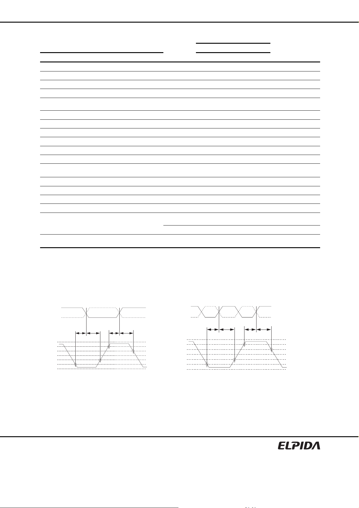
4. The figures of Input Waveform Timing 1 and 2 are referenced from the input signal crossing at the
VIH(AC) level for a rising signal and VIL(AC) for a falling signal applied to the device under test.
5. The figures of Input Waveform Timing 1 and 2 are referenced from the input signal crossing at the
VIL(DC) level for a rising signal and VIH(DC) for a falling signal applied to the device under test.
DQS
/DQS
tDS tDH
Input Waveform Timing 1 (tDS, tDH) Input Waveform Timing 2 (tIS, tIH)
Preliminary Data Sheet E1196E10 (Ver. 1.0)
tDS tDH
VDDQ
VIH (AC)(min.)
VIH (DC)(min.)
VREF
VIL (DC)(max.)
VIL (AC)(max.)
VSS
tIS tIH
tIS tIH
VDDQ
VIH (AC)(min.)
VIH (DC)(min.)
VREF
VIL (DC)(max.)
VIL (AC)(max.)
VSS
17
EDE2104ABSE, EDE2108ABSE
6. tHP is the minimum of the absolute half period of the actua l input clock. tHP is an input parameter but not
an input specification parameter. It is used in conjunction with tQHS to derive the DRAM output timing
tQH.
The value to be used for tQH calculation is determined by the following equation;
tHP = min ( tCH(abs), tCL(abs) ),
where,
tCH(abs) is the minimum of the actual instantaneous clock high time;
tCL(abs) is the minimum of the actual instantaneous clock low time;
7. tQHS accounts for:
a. The pulse duration distortion of on-chip clock ci rcuits, which represents ho w well the actual tHP at the
input is transferred to the output; and
b. The worst case push-out of DQS on one transition followed by the worst case pull-i n of DQ on the
next transition, both of which are independent of each other, due to data pin ske w, output pattern effects,
and p-channel to n-channel variation of the output drivers.
8. tQH = tHP – tQHS, where:
tHP is the minimum of the absolute half period of the actual input clock; and tQHS is the specification
value under the max column.
{The less half-pulse width distortion pr esent, the larger the tQH value is; a nd the larger the valid data e ye
will be.}
Examples:
a. If the system provides tHP of 1315ps into a DDR2-667 SDRAM, the DRAM provides tQH of 975ps
(min.)
b. If the system provides tHP of 1420ps into a DDR2-667 SDRAM, the DRAM provides tQH of 1080ps
(min.)
9. RU stands for round up. WR refers to the tWR parameter stored in the MRS.
10. When the device is operated with input clock jitter, this parameter needs to be derated by the actual
tERR(6-10per) of the input clock. (output deratings are relative to the SDRAM input clock.)
For example, if the measured jitter into a DDR2-667 SDRAM has tERR(6-10per) min. = −272ps and
tERR(6-10per) max. = +293ps, then tDQSCK min.(derated) = tDQSCK min. − tERR(6-10per) max. =
−400ps − 293ps = −693ps and tDQSCK max.(derated) = tDQSCK max. − tERR(6-10per) min. = 400ps +
272ps = +672ps. Similarly, tLZ(DQ) for DDR2-667 derates to tLZ(DQ) min.(derated) = −900ps − 293ps =
−1193ps and tLZ(DQ) max.(derated)= 450ps + 272ps = +722ps.
11. When the device is operated with input clock jitter, this parameter needs to be derated by the actual
tJIT(per) of the input clock. (output deratings are relative to the SDRAM input clock.)
For example, if the measured jitter into a DDR2-667 SDRAM has tJIT(per) min. = −72ps and
tJIT(per) max. = +93ps, then tRPRE min.(derated) = tRPRE min. + tJIT(per) min. = 0.9 × tCK(avg) − 72ps
= +2178ps and tRPRE max.(derated) = tRPRE max. + tJIT(per) max. = 1.1 × tCK(avg) + 93ps = +2843ps.
12. When the device is operated with input clock jitter, this parameter needs to be derated by the actual
tJIT(duty) of the input clock. (output deratings are relative to the SDRAM input clock.)
For example, if the measured jitter into a DDR2-667 SDRAM has tJIT(duty) min. = −72ps and
tJIT(duty) max. = +93ps, then tRPST min.(derated) = tRPST min. + tJIT(duty) min. = 0.4 × tCK(avg) −
72ps = +928ps and tRPST max.(derated) = tRPST max. + tJIT(duty) max. = 0.6 × tCK(avg) + 93ps =
+1592ps.
13. Refer to the Clock Jitter table.
Preliminary Data Sheet E1196E10 (Ver. 1.0)
18
EDE2104ABSE, EDE2108ABSE
ODT AC Electrical Characteristics
Parameter Symbol min. max. Unit Notes
ODT turn-on delay tAOND 2 2 tCK
ODT turn-on
-8G, -6E
-5C tAON tAC (min) tAC (max) + 1000 ps 1
ODT turn-on (power-down mode) tAONPD tAC(min) + 2000 2tCK + tAC(max) + 1000 ps
ODT turn-off delay tAOFD 2.5 2.5 tCK 5, 6
ODT turn-off tAOF tAC(min) tAC(max) + 600 ps 2, 4, 5, 6
ODT turn-off (power-down mode) tAOFPD tAC(min) + 2000 2.5tCK + tAC(max) + 1000 ps
ODT to power-down entry latency tANPD 3 3 tCK
ODT power-down exit latency tAXPD 8 8 tCK
Notes: 1. ODT turn on time min is when the device leaves high impedance and ODT resistance begins to turn on.
ODT turn on time max is when the ODT resistance is fully on. Both are measured from tAOND.
2. ODT turn off time min is when the device starts to turn off ODT resistance.
ODT turn off time max is when the bus is in high impedance. Both are measured from tAOFD.
3. When the device is operated with input clock jitter, this parameter needs to be derated by the actual
tERR(6-10per) of the input clock. (output deratings are relative to the SDRAM input clock.)
4. When the device is operated with input clock jitter, this parameter needs to be derated by
{−tJIT(duty) max. − tERR(6-10per) max. } and { −tJIT(duty) min. − tERR(6-10per) min. } of the actual input
clock.(output deratings are relative to the SDRAM input clock.)
For example, if the measured jitter into a DDR2-667 SDRAM has tERR(6-10per) min. = −272ps,
tERR(6-10per) max. = +293ps, tJIT(duty) min. = −106ps and tJIT(duty) max. = +94ps, then
tAOF min.(derated) = tAOF min. + { −tJIT(duty) max. − tERR(6-10per) max. } = −450ps + { −94ps − 293ps}
= −837ps and tAOF max.(derated) = tAOF max. + { −tJIT(duty) min. − tERR(6-10per) min. } = 1050ps +
{ 106ps + 272ps} = +1428ps.
5. For tAOFD of DDR2-533, the 1/2 clock of tCK in the 2.5 × tCK assumes a tCH, input clock high pulse
width of 0.5 relative to tCK. tAOF min. and tAOF max. should each be derated by t he same amount as
the actual amount of tCH offset present at the DRAM input with respect to 0.5. For example, if an input
clock has a worst case tCH of 0.45, the tAOF min. should be derated by subtracting 0.05 × tCK from it,
whereas if an input clock has a worst case tCH of 0.55, the tAOF max. should be derated by adding 0.05
× tCK to it. Therefore, we have;
tAOF min.(derated) = tAC min. − [0.5 − Min.(0.5, tCH min.)] × tCK
tAOF max.(derated) = tAC max. + 0.6 + [Max.(0.5, tCH max.) − 0.5] × tCK
or
tAOF min.(derated) = Min.(tAC min., tAC min. − [0.5 − tCH min.] × tCK)
tAOF max.(derated) = 0.6 + Max.(tAC max., tAC max. + [tCH max. − 0.5] × tCK)
where tCH min. and tCH max. are the m inimum and maximum of tCH actually measured at the DRAM
input balls.
6. For tAOFD of DDR2-667/800, the 1/2 clock of nCK in the 2.5 ×
clock high pulse width of 0.5 relative to tCK(avg). tAOF min. and tAOF max. should each be d erated by
the same amount as the actual amount of tCH(avg) offset present at the DRAM input with respect to 0.5.
For example, if an input clock has a worst case tCH(avg) of 0.48, the tAOF min. should be derated by
subtracting 0.02 × tCK(avg) from it, whereas if an input clock has a worst case tCH(avg) of 0.52,
the tAOF max. should be derated by adding 0.02 × tCK(avg) to it. Therefore, we have;
tAOF min.(derated) = tAC min. − [0.5 − Min.(0.5, tCH(avg) min.)] × tCK(avg)
tAOF max.(derated) = tAC max. + 0.6 + [Max.(0.5, tCH(avg) max.) − 0.5] × tCK(avg)
or
tAOF min.(derated) = Min.(tAC min., tAC min. − [0.5 − tCH(avg) min.] × tCK(avg))
tAOF max.(derated) = 0.6 + Max.(tAC max., tAC max. + [tCH(avg) max. − 0.5] × tCK(avg))
where tCH(avg) min. and tCH(avg) max. are the minimum and ma ximum of tCH(avg) actually measured
at the DRAM input balls.
tAON tAC (min) tAC (max) + 700 ps 1, 3
nCK assumes a tCH(avg), average input
Preliminary Data Sheet E1196E10 (Ver. 1.0)
19
EDE2104ABSE, EDE2108ABSE
AC Input Test Conditions
Parameter Symbol Value Unit Notes
Input reference voltage VREF 0.5 × VDDQ V 1
Input signal maximum peak to peak swing VSWING (max.) 1.0 V 1
Input signal minimum slew rate SLEW 1.0 V/ns 2, 3
Notes: 1. Input waveform timing is referenced to the input signal crossing through the VIH/IL (AC) level applied to
the device under test.
2. The input signal minimum sle w rate is to be maintained over the range from VREF to VIH (AC) min. for
rising edges and the range from VREF to VIL (AC) max. for falling edges as shown in the below figure.
3. AC timings are referenced with input waveforms switching from VIL (AC) to VIH (AC) on the positive
transitions and VIH (AC) to VIL (AC) on the negative transitions.
VDDQ
VIH (AC)(min.)
VIH (DC)(min.)
VSWING(max.)
VREF
VIL (DC)(max.)
VIL (AC)(max.)
Falling slew =
ΔTF
VREF
ΔTR
−
VIL (AC)(max.)
ΔTF
Rising slew =
AC Input Test Signal Wave forms
Measurement point
DQ
RT =25 Ω
Output Load
VTT
VIH (AC) min. − VREF
VSS
ΔTR
Preliminary Data Sheet E1196E10 (Ver. 1.0)
20
EDE2104ABSE, EDE2108ABSE
Clock Jitter [DDR2-800, 667]
-8G -6E
Frequency (Mbps) 800 667
Parameter Symbol min. max. min. max. Unit Notes
Average clock period tCK (avg) 2500 8000 3000 8000 ps 1
Clock period jitter tJIT (per) −100 100 −125 125 ps 5
Clock period jitter during
DLL locking period
Cycle to cycle period jitter tJIT (cc) ⎯ 200 ⎯ 250 ps 6
Cycle to cycle clock period jitter
during DLL locking period
Cumulative error across 2 cycles tERR (2per) −150 150 −175 175 ps 7
Cumulative error across 3 cycles tERR (3per) −175 175 −225 225 ps 7
Cumulative error across 4 cycles tERR (4per) −200 200 −250 250 ps 7
Cumulative error across 5 cycles tERR (5per) −200 200 −250 250 ps 7
Cumulative error across
n=6,7,8,9,10 cycles
Cumulative error across
n=11, 12,…49,50 cycles
Average high pulse width tCH (avg) 0.48 0.52 0.48 0.52 tCK (avg) 2
Average low pulse width tCL (avg) 0.48 0.52 0.48 0.52 tCK (avg) 3
Duty cycle jitter tJIT (duty) −100 100 −125 125 ps 4
Notes: 1. tCK (avg) is calculated as the average clock period across any consecutive 200cycle window.
tJIT
(per, lck)
tJIT (cc, lck) ⎯ 160 ⎯ 200 ps 6
tERR
(6-10per)
tERR
(11-50per)
−80 80 −100 100 ps 5
−300 300 −350 350 ps 7
−450 450 −450 450 ps 7
N
⎧
=
)(
⎨
∑
=1
j
⎩
N = 200
2. tCH (avg) is defined as the average high pulse width, as calculated across any consecutive 200 high
pulses.
N
⎧
=
⎨
∑
j
=
⎩
3. tCL (avg) is defined as the average low pulse width, as calculated across a ny consecutive 200 low pulses.
N
⎧
=
⎨
∑
j
=
⎩
4. tJIT (duty) is defined as the cumulative set of tCH jitter and tCL jitter. tCH jitter is the largest deviation of
any single tCH from tCH (avg). tCL jitter is the largest deviation of any single tCL from tCL (avg).
tJIT (duty) is not subject to production test.
tJIT (duty) = Min./Max. of {tJIT (CH), tJIT (CL)}, where:
tJIT (CH) = {tCH
tJIT (CL) = {tCL
5. tJIT (per) is defined as the largest deviation of any single tCK from tCK (avg).
tJIT (per) = Min./Max. of { tCK
tJIT (per) defines the single period jitter when the DLL is already locked. tJIT (per, lck) uses the same
definition for single period jitter, during the DLL locking period only. tJIT (per) and tJIT (per, lck) are not
subject to production test.
- tCH (avg) where j = 1 to 200}
j
− tCL (avg) where j = 1 to 200}
j
− tCK (avg) where j = 1 to 200}
j
1
N = 200
1
N = 200
⎫
⎬
⎭
⎫
⎬
⎭
⎫
NtCKjavgtCK
⎬
⎭
))(()(
×
×
avgtCKNtCHjavgtCH
))(()(
avgtCKNtCLjavgtCL
Preliminary Data Sheet E1196E10 (Ver. 1.0)
21
EDE2104ABSE, EDE2108ABSE
6. tJIT (cc) is defined as the absolute difference in clock period between two consec utive clock cycles:
tJIT (cc) = Max. of |tCK
tJIT (cc) is defines the cycle to cycle jitter when the DLL is already locked. tJIT (cc, lck) uses the same
definition for cycle to cycle jitter, during the DLL locking period only. tJIT (cc) and tJIT (cc, lck) are not
subject to production test.
7. tERR (nper) is defined as the cumulative error across multiple consecutive cycles from tCK (avg).
tERR (nper) is not subject to production test.
8. These parameters are specified per their average values, however it is understood that the following
relationship between the average timing and the absolute instantaneous timing hold at all times.
(minimum and maximum of spec values are to be used for calculations in the table below.)
Parameter Symbol min. max. Unit
Absolute clock period tCK (abs) tCK (avg) min. + tJIT (per) min. tCK (avg) max. + tJIT (per) max. ps
Absolute clock high pulse
width
Absolute clock low pulse
width
Example: For DDR2-667, tCH(abs) min. = ( 0.48 × 3000 ps ) - 125ps = 1315ps
− tCKj|
j+1
tCH (abs)
tCL (abs)
n
⎧
=
⎨
∑
=
j
⎩
2 ≤ n ≤ 50 for tERR (nper)
tCH (avg) min. × tCK (avg) min. +
tJIT (duty) min.
tCL (avg) min. × tCK (avg) min. +
tJIT (duty) min.
⎫
×−
⎬
1
⎭
))()(
avgtCKntCKjnpertERR
tCH (avg) max. × tCK (avg) max.
+ tJIT (duty) max.
tCL (avg) max. × tCK (avg) max.
+ tJIT (duty) max.
ps
ps
Preliminary Data Sheet E1196E10 (Ver. 1.0)
22
EDE2104ABSE, EDE2108ABSE
Input Slew Rate Derating
For all input signals the total tIS, tDS (setup time) and tIH, tDH (hold time) required is calculated by adding the data
sheet tIS (base), tDS (base) and tIH (base), tDH (base) value to the ΔtIS, ΔtDS and ΔtIH, ΔtDH derating value
respectively.
Example: tDS (total setup time) = tDS (base) + ΔtDS.
Setup (tIS, tDS) nominal slew rate for a rising signal is defined as the slew rate bet ween the last crossing of VREF
(DC) and the first crossing of VIH (AC) min. Setup (tIS, tDS) nominal slew rate for a falling signal is defined as the
slew rate between the last crossing of VREF (DC) and the first crossing of VIL (AC) max. If the actual signal is
always earlier than the nominal slew rate line between shaded ‘VREF (DC) to AC region’, use nominal slew rate for
derating value (See the figure of Slew Rate Definition Nominal).
If the actual signal is later than the nominal slew rate line anywhere between shaded ‘VREF (DC) to AC region’, the
slew rate of a tangent line to the actual signal from the AC level to DC level is used for derating value (see the figure
of Slew Rate Definition Tangent).
Hold (tIH, tDH) nominal slew rate for a rising signal is defined as the slew rate between the last crossing of
VIL (DC) max. and the first crossing of VREF (DC). Hold (tIH, tDH) nominal slew rate for a falling signal is defined
as the slew rate between the last crossing of VIH (DC) min. and the first crossing of VRE F (DC). If the actual signal
is always later than the nominal slew rate line between shaded ‘DC lev el to VREF (DC) region’, use nominal slew
rate for derating value (See the figure of Slew Rate Definition Nominal).
If the actual signal is earlier than the nominal slew rate line anywhere between shaded ‘DC to VREF (DC) region’,
the slew rate of a tangent line to the actual signal from the DC level to VREF (DC) level is used for derating value
(see the figure of Slew Rate Definition Tangent).
Although for slow slew rates the total setup time might be negative (i.e. a valid i nput signal will not have reached
VIH/IL (AC) at the time of the rising clock transition) a valid input signal is still required to complete the transition and
reach VIH/IL (AC).
For slew rates in between the values listed in the tables below, the derating values may obtained by linear
interpolation.
These values are typically not subject to production test. They are verified by design and characterization.
[Derating Values of tDS/tDH with Differential DQS (DDR2-533)]
DQS, /DQS differential slew rate
4.0 V/ns 3.0 V/ns 2.0 V/ns 1.8 V/ns 1.6 V/ns 1.4 V/ns 1.2 V/ns 1.0 V/ns 0.8 V/ns
ΔtDS ΔtDH ΔtDS ΔtDH ΔtDS ΔtDH ΔtDS ΔtDH ΔtDS ΔtDH ΔtDS ΔtDH ΔtDS ΔtDH ΔtDS ΔtDH ΔtDS ΔtDH Unit
2.0 +125 +45 +125 +45 +125 +45 ⎯ ⎯ ⎯ ⎯ ⎯ ⎯ ⎯ ⎯ ⎯ ⎯ ⎯ ⎯ ps
1.5 +83 +21 +83 +21 +83 +21 +95 +33 ⎯ ⎯ ⎯ ⎯ ⎯ ⎯ ⎯ ⎯ ⎯ ⎯ ps
1.0 0 0 0 0 0 0 +12 +12 +24 +24 ⎯ ⎯ ⎯ ⎯ ⎯ ⎯ ⎯ ⎯ ps
DQ
slew
rate
(V/ns)
0.9 ⎯ ⎯ −11 −14 −11 −14 +1 −2 +13 +10 +25 +22 ⎯ ⎯ ⎯ ⎯ ⎯ ⎯ ps
0.8 ⎯ ⎯ ⎯ ⎯ −25 −31 −13 −19 −1 −7 11 +5 +23 +17 ⎯ ⎯ ⎯ ⎯ ps
0.7 ⎯ ⎯ ⎯ ⎯ ⎯ ⎯ −31 −42 −19 −30 −7 −18 +5 −6 +17 +6 ⎯ ⎯ ps
0.6 ⎯ ⎯ ⎯ ⎯ ⎯ ⎯ ⎯ ⎯ −43 −59 −31 −47 −19 −35 −7 −23 +5 −11 ps
0.5 ⎯ ⎯ ⎯ ⎯ ⎯ ⎯ ⎯ ⎯ ⎯ ⎯ −74 −89 −62 −77 −50 −65 −38 −53 ps
0.4 ⎯ ⎯ ⎯ ⎯ ⎯ ⎯ ⎯ ⎯ ⎯ ⎯ ⎯ ⎯ −127 −140 −115 −128 −103 −116 ps
Preliminary Data Sheet E1196E10 (Ver. 1.0)
23
EDE2104ABSE, EDE2108ABSE
[Derating Values of tDS/tDH with Differential DQS (DDR2-667, 800)
DQS, /DQS differential slew rate
4.0 V/ns 3.0 V/ns 2.0 V/ns 1.8 V/ns 1.6 V/ns 1.4 V/ns 1.2 V/ns 1.0 V/ns 0.8 V/ns
ΔtDS ΔtDH ΔtDS ΔtDH ΔtDS ΔtDH ΔtDS ΔtDH ΔtDS ΔtDH ΔtDS ΔtDH ΔtDS ΔtDH ΔtDS ΔtDH ΔtDS ΔtDH Unit
2.0 +100 +45 +100 +45 +100 +45 ⎯ ⎯ ⎯ ⎯ ⎯ ⎯ ⎯ ⎯ ⎯ ⎯ ⎯ ⎯ ps
1.5 +67 +21 +67 +21 +67 +21 +79 +33 ⎯ ⎯ ⎯ ⎯ ⎯ ⎯ ⎯ ⎯ ⎯ ⎯ ps
1.0 0 0 0 0 0 0 +12 +12 +24 +24 ⎯ ⎯ ⎯ ⎯ ⎯ ⎯ ⎯ ⎯ ps
DQ
slew
rate
(V/ns)
0.9 ⎯ ⎯ −5 −14 −5 −14 +7 −2 +19 +10 +31 +22 ⎯ ⎯ ⎯ ⎯ ⎯ ⎯ ps
0.8 ⎯ ⎯ ⎯ ⎯ −13 −31 −1 −19 +11 −7 +23 +5 +35 +17 ⎯ ⎯ ⎯ ⎯ ps
0.7 ⎯ ⎯ ⎯ ⎯ ⎯ ⎯ −10 −42 +2 −30 +14 −18 +26 −6 +38 +6 ⎯ ⎯ ps
0.6 ⎯ ⎯ ⎯ ⎯ ⎯ ⎯ ⎯ ⎯ −10 −59 +2 −47 +14 −35 +26 −23 +38 −11 ps
0.5 ⎯ ⎯ ⎯ ⎯ ⎯ ⎯ ⎯ ⎯ ⎯ ⎯ −24 −89 −12 −77 0 −65 +12 −53 ps
0.4 ⎯ ⎯ ⎯ ⎯ ⎯ ⎯ ⎯ ⎯ ⎯ ⎯ ⎯ ⎯ −52 −140 −40 −128 −28 −116 ps
[Derating Values of tDS1/tDH1 with Single-Ended DQS (DDR2-533)]
DQS, /DQS single-ended slew rate
2.0 V/ns 1.5 V/ns 1.0V/ns 0.9V/ns 0.8V/ns 0.7 V/ns 0.6 V/ns 0.5 V/ns 0.4 V/ns
DQ
slew
rate
(V/ns)
Δ
tDS1 Δ tDH1 Δ tDS1Δ tDH1 Δ tDS1 Δ tDH1Δ tDS1Δ tDH1Δ tDS1Δ tDH1Δ tDS1Δ tDH1Δ tDS1Δ tDH1 Δ tDS1 Δ tDH1 Δ tDS1 Δ tDH1
2.0 +188 +188 +167 +146 +125 +63 ⎯ ⎯ ⎯ ⎯ ⎯ ⎯ ⎯ ⎯ ⎯ ⎯ ⎯ ⎯ ps
1.5 +146 +167 +125 +125 +83 +42 +81 +43 ⎯ ⎯ ⎯ ⎯ ⎯ ⎯ ⎯ ⎯ ⎯ ⎯ ps
1.0 +63 +125 +42 +83 0 0 −2 +1 −7 −13 ⎯ ⎯ ⎯ ⎯ ⎯ ⎯ ⎯ ⎯ ps
0.9 ⎯ ⎯ +31 +69 −11 −14 −13 −13 −18 −27 −29 −45 ⎯ ⎯ ⎯ ⎯ ⎯ ⎯ ps
0.8 ⎯ ⎯ ⎯ ⎯ −25 −31 −27 −30 −32 −44 −43 −62 −60 −86 ⎯ ⎯ ⎯ ⎯ ps
0.7 ⎯ ⎯ ⎯ ⎯ ⎯ ⎯ −45 −53 −50 −67 −61 −85 −78 −109 −108 −152 ⎯ ⎯ ps
0.6 ⎯ ⎯ ⎯ ⎯ ⎯ ⎯ ⎯ ⎯ −74 −96 −85 −114 −102 −138 −132 −181 −183 −246 ps
0.5 ⎯ ⎯ ⎯ ⎯ ⎯ ⎯ ⎯ ⎯ ⎯ ⎯ −128 −156 −145 −180 −175 −223 −226 −288 ps
0.4 ⎯ ⎯ ⎯ ⎯ ⎯ ⎯ ⎯ ⎯ ⎯ ⎯ ⎯ ⎯ −210 −243 −240 −286 −291 −351 ps
Unit
Preliminary Data Sheet E1196E10 (Ver. 1.0)
24
EDE2104ABSE, EDE2108ABSE
[Derating Values of tIS/tIH (DDR2-533)]
CK, /CK Differential Slew Rate
2.0 V/ns 1.5 V/ns 1.0 V/ns
ΔtIS ΔtIH ΔtIS ΔtIH ΔtIS ΔtIH Unit Notes
4.0 +187 +94 +217 +124 +247 +154 ps
3.5 +179 +89 +209 +119 +239 +149 ps
3.0 +167 +83 +197 +113 +227 +143 ps
2.5 +150 +75 +180 +105 +210 +135 ps
2.0 +125 +45 +155 +75 +185 +105 ps
1.5 +83 +21 +113 +51 +143 +81 ps
1.0 0 0 +30 +30 +60 60 ps
0.9 −11 −14 +19 +16 +49 +46 ps
Command/address
slew rate (V/ns)
0.8 −25 −31 +5 −1 +35 +29 ps
0.7 −43 −54 −13 −24 +17 +6 ps
0.6 −67 −83 −37 −53 −7 −23 ps
0.5 −110 −125 −80 −95 −50 −65 ps
0.4 −175 −188 −145 −158 −115 −128 ps
0.3 −285 −292 −255 −262 −225 −232 ps
0.25 −350 −375 −320 −345 −290 −315 ps
0.2 −525 −500 −495 −470 −465 −440 ps
0.15 −800 −708 −770 −678 −740 −648 ps
0.1 −1450 −1125 −1420 −1095 −1390 −1065 ps
Preliminary Data Sheet E1196E10 (Ver. 1.0)
25

EDE2104ABSE, EDE2108ABSE
[Derating Values of tIS/tIH (DDR2-667, DDR2-800)]
CK, /CK Differential Slew Rate
2.0 V/ns 1.5 V/ns 1.0 V/ns
ΔtIS ΔtIH ΔtIS ΔtIH ΔtIS ΔtIH Unit Notes
4.0 +150 +94 +180 +124 +210 +154 ps
3.5 +143 +89 +173 +119 +203 +149 ps
3.0 +133 +83 +163 +113 +193 +143 ps
2.5 +120 +75 +150 +105 +180 +135 ps
2.0 +100 +45 +130 +75 +160 +105 ps
1.5 +67 +21 +97 +51 +127 +81 ps
1.0 0 0 +30 +30 +60 +60 ps
0.9 −5 −14 +25 +16 +55 +46 ps
Command/address
slew rate (V/ns)
0.8 −13 −31 +17 −1 +47 +29 ps
0.7 −22 −54 +8 −24 +38 +6 ps
0.6 −34 −83 −4 −53 +26 −23 ps
0.5 −60 −125 −30 −95 0 −65 ps
0.4 −100 −188 −70 −158 −40 −128 ps
0.3 −168 −292 −138 −262 −108 −232 ps
0.25 −200 −375 −170 −345 −140 −315 ps
0.2 −325 −500 −295 −470 −265 −440 ps
0.15 −517 −708 −487 −678 −457 −648 ps
0.1 −1000 −1125 −970 −1095 −940 −1065 ps
Preliminary Data Sheet E1196E10 (Ver. 1.0)
26

EDE2104ABSE, EDE2108ABSE
Single-ended DQS
VDDQ
VIH (AC) min.
DQS
Differential DQS, /DQS
DQS
CK
/DQS
/CK
VIH (AC) min.
VIH (DC) min.
VREF (DC)
VIL (DC) max.
VIL (AC) max.
VSS
CK, /CK
VDD
VREF to AC
region
tDS1 tDH1 tDS1 tDH1
tDS
tIS
tDH
tIH
tDS
tIS
tDH
tIH
VIH (DC) min.
VREF (DC)
VIL (DC) max.
VIL (AC) max.
Setup slew rate
Falling signal
Hold slew rate
Rising signal
DC to VREF
region
VSS
ΔTFS ΔTRH ΔTFHΔTRS
VREF (DC) - VIL (AC) max.
=
ΔTFS
VREF (DC) - VIL (DC) max.
=
ΔTRH
nominal
slew rate
Setup slew rate
Rising signal
Hold slew rate
Falling signal
Slew Rate Definition Nominal
nominal
slew rate
DC to VREF
region
VREF to AC
region
VIH (AC) min.
=
ΔTRS
VIH (DC) min. - VREF (DC)
=
ΔTFH
-
VREF (DC)
Preliminary Data Sheet E1196E10 (Ver. 1.0)
27

EDE2104ABSE, EDE2108ABSE
Single-ended DQS
VDDQ
VIH (AC) min.
VIH (DC) min.
DQS
VREF (DC)
VIL (DC) max.
VIL (AC) max.
VSS
Differential DQS, /DQS
CK, /CK
DQS
CK
/DQS
/CK
tDS1 tDH1 tDS1 tDH1
VDD
VIH (AC) min.
VIH (DC) min.
VREF (DC)
VIL (DC) max.
VIL (AC) max.
VREF to AC
region
DC to VREF
region
nominal
line
tDS
tIS
tangent
line
tDH
tIH
nominal
line
nominal
line
tDS
tIS
tangent
line
VREF to AC
region
tDH
tIH
nominal
line
DC to VREF
region
VSS
ΔTFS ΔTRH ΔTFHΔTRS
Setup slew rate
Falling signal
Hold slew rate
Rising signal
tangent line [VREF (DC) - VIL (AC) max.]
=
tangent line [VREF (DC) - VIL (DC) max.]
=
Δ
TFS
Δ
TRH
Setup slew rate
Rising signal
Hold slew rate
Falling signal
tangent line [VIH (AC) min.
=
tangent line [VIH (DC) min. - VREF (DC)]
=
Δ
TRS
Δ
- VREF (DC)]
TFH
Slew Rate Definition Tangent
Preliminary Data Sheet E1196E10 (Ver. 1.0)
28

Block Diagram
CK
/CK
CKE
Clock
generator
EDE2104ABSE, EDE2108ABSE
Bank 7
Bank 6
Bank 5
Bank 4
Bank 3
Bank 2
Bank 1
Address,
BA0, BA1, BA2
/CS
/RAS
/CAS
/WE
Mode
register
Control logic
Command decoder
Row
address
buffer
and
refresh
counter
Column
address
buffer
and
burst
counter
Memory cell array
Bank 0
Row decoder
Sense amp.
Column decoder
Data control circuit
Latch circuit
DLLCK, /CK
Input & Output buffer
DQS, /DQS
RDQS, /RDQS
ODT
DM
DQ
Preliminary Data Sheet E1196E10 (Ver. 1.0)
29

EDE2104ABSE, EDE2108ABSE
Pin Function
CK, /CK (input pins)
CK and /CK are differential clock inputs. All address and control input signals are sampled on the crossing of the
positive edge of CK and negative edge of /CK. Output (read) data is referenced to the crossings of CK and /CK
(both directions of crossing).
/CS (input pin)
All commands are masked when /CS is registered high. /CS provides for external r ank selection on systems with
multiple ranks. /CS is considered part of the command code.
/RAS, /CAS, /WE (input pins)
/RAS, /CAS and /WE (along with /CS) define the command being entered.
A0 to A14 (input pins)
Provided the row address for Active commands and the column address and Auto Precharge bit for Read/Write
commands to select one location out of the memory array in the res pective bank. The address inputs also provide
the op-code during mode register set commands.
[Address Pins Table]
Address (A0 to A14)
Part number Row address Column address
EDE2104ABSE AX0 to AX14 AY0 to AY9, AY11
EDE2108ABSE AX0 to AX14 AY0 to AY9
A10 (AP) (input pin)
A10 is sampled during a precharge command to determine whether the precharge applies to one ban k (A10 = low)
or all banks (A10 = high). If only one bank is to be precharged, the bank is selected by BA0, BA1 and BA2.
BA0, BA1, BA2 (input pins)
BA0, BA1 and BA2 define to which bank an active, read, write or precharge command is being applied. BA0 and
BA1 also determine if the mode register or extended mode register is to be acc essed during a MRS or EMRS (1),
EMRS (2) cycle.
[Bank Select Signal Table]
BA0 BA1 BA2
Bank 0 L L L
Bank 1 H L L
Bank 2 L H L
Bank 3 H H L
Bank 4 L L H
Bank 5 H L H
Bank 6 L H H
Bank 7 H H H
Remark: H: VIH. L: VIL.
Note
Preliminary Data Sheet E1196E10 (Ver. 1.0)
30

EDE2104ABSE, EDE2108ABSE
CKE (input pin)
CKE high activates, and CKE low deactivates, internal clock signals and device input buffers and output drivers.
Taking CKE low provides precharge power-down and Self-Ref resh operation (all banks idle), or active power-down
(row active in any bank). CKE is synchronous for power-down entry and exit, and for self-refresh entry. CKE is
asynchronous for self-refresh exit. CKE must be maintained high throughout read and write accesses. Input buffers,
excluding CK, /CK and CKE are disabled during power-down. Input buffers, excl uding CKE, are disabled during selfrefresh.
DM (input pins)
DM is an input mask signal for write data. Input data is masked when DM is sampled high coincident with that input
data during a Write access. DM is sampled on both edges of DQS. Although DM pins are input only, the DM
loading matches the DQ and DQS loading.
For ×8 configuration, DM function will be disabled when RDQS function is enabled by EMRS.
DQ (input/output pins)
Bi-directional data bus.
DQS, /DQS (input/output pins)
Output with read data, input with write data for source synchronous operation. Edge-aligned with read data,
centered in write data. Used to capture write data. /DQS can be disabled by EMRS.
RDQS, /RDQS (output pins)
Differential Data Strobe for READ operation only. DM and RDQS functions are switch able by EMRS. These pins
exist only in ×8 configuration. /RDQS output will be disabled when /DQS is disabled by EMRS.
ODT (input pins)
ODT (On Die Termination control) is a registered high signal that enables terminatio n resistance internal to the DDR
2 SDRAM. When enabled, ODT is only applied to each DQ, DQS, /DQS, RDQS, /RDQS, and DM signal for × 4, × 8
configurations. The ODT pin will be ignored if the Extended Mode Register (EMRS) is programmed to disable ODT .
Any time the EMRS enables the ODT function; ODT may not be driven high until eight clocks after the EMRS has
been enabled.
VDD, VSS, VDDQ, VSSQ (power supply)
VDD and VSS are power supply pins for internal circuits. VDDQ and VSSQ are po wer supply pins for the output
buffers.
VDDL and VSSDL (power supply)
VDDL and VSSDL are power supply pins for DLL circuits.
VREF (Power supply)
SSTL_18 reference voltage: (0.50 ± 0.01) × VDDQ
Preliminary Data Sheet E1196E10 (Ver. 1.0)
31

EDE2104ABSE, EDE2108ABSE
Command Operation
Command Truth Table
The DDR2 SDRAM recognizes the following commands specified by the /CS, /RAS, /CAS, /WE and address pins.
CKE
Function
Mode register set MRS H H L L L L L L L MRS OPCODE 1
Extended mode
register set (1)
Extended mode
register set (2)
Auto-refresh REF H H L L L H × × × × × × 1
Self-refresh entry SELF H L L L L H × × × × × × 1
Self-refresh exit SELFX L H H × × × × × × × × × 1, 6
L H L H H H × × × × × ×
Single bank precharge PRE H H L L H L BA
Precharge all banks PALL H H L L H L × × × × H × 1
Bank activate ACT H H L L H H BA RA 1, 2, 7
Write WRIT H H L H L L BA
Write with auto precharge WRITA H H L H L L BA
Read READ H H L H L H BA
Read with auto precharge READA H H L H L H BA
No operation NOP H × L H H H × × × × × × 1
Device deselect DESL H × H × × × × × × × × × 1
Power-down mode entry PDEN H L H × × × × × × × × × 1, 4
H L L H H H × × × × × ×
Power-down mode exit PDEX L H H × × × × × × × × × 1, 4
L H L H H H × × × × × ×
Symbol
EMRS(1) H H L L L L H L L
EMRS(2) H H L L L L L H L
Previous
cycle
Current
cycle /CS /RAS /CAS /WE BA0 BA1 BA2
Remark: H = VIH. L = VIL. × = VIH or VIL. BA = Bank Address, RA = Row Address , CA = Column Address
Notes: 1. All DDR2 commands are d efined by states of /CS, /RAS, /CAS, /WE and CKE at the rising edge of the
clock.
2. Bank select (BA0, BA1 and BA2), determine which bank is to be operated upon.
3. Burst reads or writes should not be terminated other than specified as ″Reads interrupte d by a Read″ in
burst read command [READ] or ″Writes interrupted by a Write″ in burst write command [WRIT].
4. The power-down mode does not perform any refresh operations. The duration of power-do wn is therefore
limited by the refresh requirements of the device. One clock delay is required for mode entry and exit.
5. The state of ODT does not affect the states described in this table. The ODT function is not available
during self-refresh.
6. Self-refresh exit is asynchronous.
7. 8-bank device sequential bank activation restriction: No more than 4 banks may be activated in a rolling
tFAW window. Converting to clocks is done by dividing tFAW (ns) by tCK (ns) and rounding up to next
integer value. As an example of the rolling window, if (tFAW/tCK) rounds up to 10 clocks, and an activate
command is issued in clock N, no more than three further activate commands may be issued in clock N+1
through N+9.
A14 to
A11 A10
EMRS (1)
OPCODE
EMRS (2)
OPCODE
× L × 1, 2
CA L CA 1, 2, 3
CA H CA 1, 2, 3
CA L CA 1, 2, 3
CA H CA 1, 2, 3
A0 to
A9 Notes
1
1
Preliminary Data Sheet E1196E10 (Ver. 1.0)
32

CKE Truth Table
EDE2104ABSE, EDE2108ABSE
CKE
Current state*
Power-down L L × Maintain power-down 11, 13, 15
L H DESL or NOP Power-down exit 4, 8, 11, 13
Self-refresh L L × Maintain self-refresh 11, 15
L H DESL or NOP Self-refresh exit 4, 5, 9
Bank Active H L DESL or NOP Active power-down entry 4, 8, 10, 11, 13
All banks idle H L DESL or NOP Precharge power-down entry 4, 8, 10, 11, 13
H L SELF Self-refresh entry 6, 9, 11, 13
Any state other than
listed above
2
Previous
cycle (n-1)*1
H H Refer to the Command Truth Table 7
Current
cycle (n)*1
Command(n)
/CS, /RAS, /CAS, /WE
*3
Operation (n)*3
Notes
Remark: H = VIH. L = VIL. × = Don’t care
Notes: 1. CKE (n) is the logic state of CKE at clock edge n; CKE (n−1) was the state of CKE at the previous clock
edge.
2. Current state is the state of the DDR SDRAM immediately prior to clock edge n.
3. Command (n) is the command registered at clock edge n, and operation (n) is a result of Command (n).
4. All states and sequences not shown are illegal or reserved unless explicitl y described elsewhere in this
document.
5. On self-refresh exit, [DESL] or [NOP] commands must be issued on every clock edge occurring duri ng the
tXSNR period. Read commands may be issued only after tXSRD (200 clocks) is satisfied.
6. Self-refresh mode can only be entered from the all banks idle state.
7. Must be a legal command as defined in the command truth table.
8. Valid commands for power-down entry and exit are [NOP] and [DESL] only.
9. Valid commands for self-refresh exit are [NOP] and [DESL] only.
10. Power-down and self-refresh can not be ent ered while read or write operations, (extended) mode regis ter
set operations or precharge operations are in progress. See section Power-down and Self-Refresh
Command for a detailed list of restrictions.
11. Minimum CKE high time is 3 clocks; minimum CKE low time is 3 clocks.
12. The state of ODT does not affect the states described in this table. The ODT function is not availabl e
during self-refresh. See section ODT (On Die Termination).
13. The power-down does not perform any refresh operations. The duration of power-down mode is therefore
limited by the refresh requirements outlined in section automatic refresh command.
14. CKE must be maintained high while the SDRAM is in OCD calibration mode.
15. “×” means “don’t care” (including floating around VREF) in self-refresh and po wer-down. However ODT
must be driven high or low in power-down if the ODT function is enabled (bit A2 or A6 set to “1” in EMRS
(1) ).
Preliminary Data Sheet E1196E10 (Ver. 1.0)
33

EDE2104ABSE, EDE2108ABSE
Function Truth Table
The following tables show the operations that are performed when each comman d is issued in each state of the
DDR SDRAM.
Current state /CS /RAS /CAS /WE Address Command Operation Notes
Idle H × × × × DESL Nop
L H H H × NOP Nop
L H L H BA, CA, A10 (AP) READ/READA ILLEGAL 1
L H L L BA, CA, A10 (AP) WRIT/WRITA ILLEGAL 1
L L H H BA, RA ACT Row activating
L L H L BA PRE Nop
L L H L A10 (AP) PALL Nop
L L L H × REF Auto-refresh 2
L L L H × SELF Self-refresh 2
L L L L BA, MRS-OPCODE MRS Mode register accessing 2
L L L L BA, EMRS-OPCODE EMRS (1) (2) Extended mode register accessing 2
Bank(s) active H × × × × DESL Nop
L H H H × NOP Nop
L H L H BA, CA, A10 (AP) READ/READA Begin Read
L H L L BA, CA, A10 (AP) WRIT/WRITA Begin Write
L L H H BA, RA ACT ILLEGAL 1
L L H L BA PRE Precharge
L L H L A10 (AP) PALL Precharge all banks
L L L H × REF ILLEGAL
L L L H × SELF ILLEGAL
L L L L BA, MRS-OPCODE MRS ILLEGAL
L L L L BA, EMRS-OPCODE EMRS (1) (2) ILLEGAL
Read H × × × × DESL
L H H H × NOP
L H L H BA, CA, A10 (AP) READ/READA Burst interrupt 1, 4
L H L L BA, CA, A10 (AP) WRIT/WRITA ILLEGAL 1
L L H H BA, RA ACT ILLEGAL 1
L L H L BA PRE ILLEGAL 1, 8
L L H L A10 (AP) PALL ILLEGAL 8
L L L H × REF ILLEGAL
L L L H × SELF ILLEGAL
L L L L BA, MRS-OPCODE MRS ILLEGAL
L L L L BA, EMRS-OPCODE EMRS (1) (2) ILLEGAL
Continue burst to end -> Row
active
Continue burst to end -> Row
active
Preliminary Data Sheet E1196E10 (Ver. 1.0)
34

EDE2104ABSE, EDE2108ABSE
Current state /CS /RAS /CAS /WE Address Command Operation Note
Write H × × × × DESL
L H H H × NOP
L H L H BA, CA, A10 (AP) READ/READA ILLEGAL 1
L H L L BA, CA, A10 (AP) WRIT/WRITA Burst interrupt 1, 4
L L H H BA, RA ACT ILLEGAL 1
L L H L BA PRE ILLEGAL 1, 8
L L H L A10 (AP) PALL ILLEGAL 8
L L L H × REF ILLEGAL
L L L H × SELF ILLEGAL
L L L L BA, MRS-OPCODE MRS ILLEGAL
L L L L
Read with auto
precharge
L H H H × NOP
L H L H BA, CA, A10 (AP) READ/READA ILLEGAL 1, 7
L H L L BA, CA, A10 (AP) WRIT/WRITA ILLEGAL 1, 7
L L H H BA, RA ACT ILLEGAL 1, 7
L L H L BA PRE ILLEGAL 1, 7, 8
L L H L A10 (AP) PALL ILLEGAL 7, 8
L L L H × REF ILLEGAL
L L L H × SELF ILLEGAL
L L L L BA, MRS-OPCODE MRS ILLEGAL
L L L L
Write with auto
Precharge
L H H H × NOP
L H L H BA, CA, A10 (AP) READ/READA ILLEGAL 1, 7
L H L L BA, CA, A10 (AP) WRIT/WRITA ILLEGAL 1, 7
L L H H BA, RA ACT ILLEGAL 1, 7
L L H L BA PRE ILLEGAL 1, 7, 8
L L H L A10 (AP) PALL ILLEGAL 7, 8
L L L H × REF ILLEGAL
L L L H × SELF ILLEGAL
L L L L BA, MRS-OPCODE MRS ILLEGAL
L L L L
H × × × × DESL
H × × × × DESL
BA, EMRSOPCODE
BA, EMRSOPCODE
BA, EMRSOPCODE
EMRS (1) (2) ILLEGAL
EMRS (1) (2) ILLEGAL
EMRS (1) (2) ILLEGAL
Continue burst to end
-> Write recovering
Continue burst to end
-> Write recovering
Continue burst to end ->
Precharging
Continue burst to end ->
Precharging
Continue burst to end
->Write recovering with auto
precharge
Continue burst to end
->Write recovering with auto
precharge
Preliminary Data Sheet E1196E10 (Ver. 1.0)
35

EDE2104ABSE, EDE2108ABSE
Current state /CS /RAS /CAS /WE Address Command Operation Note
Precharging H × × × × DESL Nop -> Enter idle after tRP
L H H H × NOP Nop -> Enter idle after tRP
L H L H BA, CA, A10 (AP) READ/READA ILLEGAL 1
L H L L BA, CA, A10 (AP) WRIT/WRITA ILLEGAL 1
L L H H BA, RA ACT ILLEGAL 1
L L H L BA PRE Nop -> Enter idle after tRP 1, 8
L L H L A10 (AP) PALL Nop -> Enter idle after tRP 8
L L L H × REF ILLEGAL
L L L H × SELF ILLEGAL
L L L L BA, MRS-OPCODE MRS ILLEGAL
L L L L BA, EMRS-OPCODE EMRS (1) (2) ILLEGAL
Row activating H × × × × DESL
L H H H × NOP
L H L H BA, CA, A10 (AP) READ/READA ILLEGAL 1, 5
L H L L BA, CA, A10 (AP) WRIT/WRITA ILLEGAL 1, 5
L L H H BA, RA ACT ILLEGAL 1
L L H L BA PRE ILLEGAL
L L H L A10 (AP) PALL ILLEGAL
L L L H × REF ILLEGAL
L L L H × SELF ILLEGAL
L L L L BA, MRS-OPCODE MRS ILLEGAL
L L L L BA, EMRS-OPCODE EMRS (1) (2) ILLEGAL
Write recovering H × × × × DESL
L H H H × NOP
L H L H BA, CA, A10 (AP) READ/READA ILLEGAL 1, 6
L H L L BA, CA, A10 (AP) WRIT/WRITA New write
L L H H BA, RA ACT ILLEGAL 1
L L H L BA PRE ILLEGAL 1
L L H L A10 (AP) PALL ILLEGAL
L L L H × REF ILLEGAL
L L L H × SELF ILLEGAL
L L L L BA, MRS-OPCODE MRS ILLEGAL
L L L L BA, EMRS-OPCODE EMRS (1) (2) ILLEGAL
Nop -> Enter bank active after
tRCD
Nop -> Enter bank active after
tRCD
Nop -> Enter bank active after
tWR
Nop -> Enter bank active after
tWR
Preliminary Data Sheet E1196E10 (Ver. 1.0)
36

EDE2104ABSE, EDE2108ABSE
Current state /CS /RAS /CAS /WE Address Command Operation Note
Write recovering
with auto
precharge
L H H H × NOP Nop -> Precharging after tWR
L H L H BA, CA, A10 (AP) READ/READA ILLEGAL 1
L H L L BA, CA, A10 (AP) WRIT/WRITA ILLEGAL 1
L L H H BA, RA ACT ILLEGAL 1
L L H L BA PRE ILLEGAL 1
L L H L A10 (AP) PALL ILLEGAL
L L L H × REF ILLEGAL
L L L H × SELF ILLEGAL
L L L L BA, MRS-OPCODE MRS ILLEGAL
L L L L BA, EMRS-OPCODE EMRS (1) (2) ILLEGAL
Refresh H × × × × DESL Nop -> Enter idle after tRFC
L H H H × NOP Nop -> Enter idle after tRFC
L H L H BA, CA, A10 (AP) READ/READA ILLEGAL
L H L L BA, CA, A10 (AP) WRIT/WRITA ILLEGAL
L L H H BA, RA ACT ILLEGAL
L L H L BA PRE ILLEGAL
L L H L A10 (AP) PALL ILLEGAL
L L L H × REF ILLEGAL
L L L H × SELF ILLEGAL
L L L L BA, MRS-OPCODE MRS ILLEGAL
L L L L BA, EMRS-OPCODE EMRS (1) (2) ILLEGAL
Mode register
accessing
L H H H × NOP Nop -> Enter idle after tMRD
L H L H BA, CA, A10 (AP) READ/READA ILLEGAL
L H L L BA, CA, A10 (AP) WRIT/WRITA ILLEGAL
L L H H BA, RA ACT ILLEGAL
L L H L BA PRE ILLEGAL
L L H L A10 (AP) PALL ILLEGAL
L L L H × REF ILLEGAL
L L L H × SELF ILLEGAL
L L L L BA, MRS-OPCODE MRS ILLEGAL
L L L L BA, EMRS-OPCODE EMRS (1) (2) ILLEGAL
H × × × × DESL Nop -> Precharging after tWR
H × × × × DESL Nop -> Enter idle after tMRD
Preliminary Data Sheet E1196E10 (Ver. 1.0)
37

EDE2104ABSE, EDE2108ABSE
Current state /CS /RAS /CAS /WE Address Command Operation Note
Extended Mode H × × × × DESL Nop -> Enter idle after tMRD
register accessing L H H H × NOP Nop -> Enter idle after tMRD
L H L H BA, CA, A10 (AP) READ/READA ILLEGAL
L H L L BA, CA, A10 (AP) WRIT/WRITA ILLEGAL
L L H H BA, RA ACT ILLEGAL
L L H L BA PRE ILLEGAL
L L H L A10 (AP) PALL ILLEGAL
L L L H × REF ILLEGAL
L L L H × SELF ILLEGAL
L L L L BA, MRS-OPCODE MRS ILLEGAL
L L L L BA, EMRS-OPCODE EMRS (1) (2) ILLEGAL
Remark: H = VIH. L = VIL. × = VIH or VIL
Notes: 1. This command may be issued for other banks, depending on the state of the banks.
2. All banks must be in "IDLE".
3. All AC timing specs must be met.
4. Only allowed at the boundary of 4 bits burst. Burst interruptions at other timings are illegal.
5. Available in case tRCD is satisfied by AL setting.
6. Available in case tWTR is satisfied.
7. The DDR2 SDRAM supports the concurrent auto-precharge feature, a read with auto-precharge
enabled,or a write with auto-precharge enabled, may be followed by any column command to other
banks, as long as that command does not interrupt the read or write data transfer, and all other related
limitations apply. (E.g. Conflict between READ data and WRITE data must be avoided.)
The minimum delay from a read or write command with auto precharge enabled, to a command to a
different bank, is summarized below.
From command
Read w/AP Read or Read w/AP BL/2 tCK
Write or Write w/AP (BL/2) + 2 tCK
Precharge or Activate 1 tCK
Write w/AP Read or Read w/AP (CL − 1) + (BL/2) + tWTR tCK
Write or Write w/AP BL/2 tCK
Precharge or Activate 1 tCK
To command (different bank, noninterrupting command)
Minimum delay
(Concurrent AP supported)
Units
Preliminary Data Sheet E1196E10 (Ver. 1.0)
38

EDE2104ABSE, EDE2108ABSE
8. T he minimum delay from the read, write and precharge co mmand to the precharge com mand to the same
bank is summarized below.
[Precharge and Auto Precharge Clarification]
From command To command
Read Precharge (to same bank as read) AL + (BL/2) + Max.(RTP, 2) − 2 tCK a, b
Precharge all AL + (BL/2) + Max.(RTP, 2) − 2 tCK a, b
Read w/AP Precharge (to same bank as read w/AP) AL + (BL/2) + Max.(RTP, 2) − 2 tCK a, b
Precharge all AL + (BL/2) + Max.(RTP, 2) − 2 tCK a, b
Write Precharge (to same bank as write) WL + (BL/2) + tWR tCK b
Precharge all WL + (BL/2) + tWR tCK b
Write w/AP Precharge (to same bank as write w/AP) WL + (BL/2) + WR tCK b
Precharge all WL + (BL/2) + WR tCK b
Precharge Precharge (to same bank as precharge) 1 tCK b
Precharge all 1 tCK b
Precharge all Precharge 1 tCK b
Precharge all 1 tCK b
a. RTP[cycles] = RU{ tRTP[ns] / tCK[ns] }, where RU stands for round up.
tCK(avg) should be used in place of tCK for DDR2-667/800.
b. F or a given bank, the prechar ge period shou ld be counted from the latest prec harge com mand, either one
bank precharge or precharge all, issued to that bank. The precharge period is satisfied after tRP
depending on the latest precharge command issued to that bank.
Minimum delay between “From
command” to “To Command“
Units
Notes
Preliminary Data Sheet E1196E10 (Ver. 1.0)
39

Simplified State Diagram
OCD
CALIBRATION
MRS
EMRS (1)
EMRS (2)
EMRS (3)
(E)MRS
INITALIZATION
SEQUENCE
PRE
IDLE
ALL BANKS
PRECHARGED
ACT
EDE2104ABSE, EDE2108ABSE
CKE_L
SELF
REFRESH
SELF
CKE_H
CKE_L
CKE_H
REF
PRECHARGE
POWER
DOWN
AUTO
REFRESH
CKE_L
WRIT
WRITA
CKE_L
ACTIVE
POWER
DOWN
WRITE
WRITA
CKE_L
CKE_H
CKE_L
WRIT
WRITA
WRITA
ACTIVATING
BANK
ACTIVE
READ
WRIT
PRE, PALL
READA
READA
PRE, PALLPRE, PALL
CKE_L
READ
READ
READ
READA
READA
PRECHARGE
Automatic sequence
Command sequence
Simplified State Diagram
Preliminary Data Sheet E1196E10 (Ver. 1.0)
40

EDE2104ABSE, EDE2108ABSE
Operation of DDR2 SDRAM
Read and write accesses to the DDR2 SDRAM are burst oriented; accesses start at a selected location and continue
for the fixed burst length of four or eight in a programmed sequence. Accesses begin with the registration of an
active command, which is then followed by a read or write command. The address bits registered coincident with
the active command is used to select the bank and row to be accessed (BA0, BA1 and BA2 sel ect the bank; A0 to
A14 select the row). The address bits registered coincident with the read or write command are used to select the
starting column location for the burst access and to determine if the auto precharge command is to be issued.
Prior to normal operation, the DDR2 SDRAM must be initialized. T he following sectio ns provide detail ed information
covering device initialization; register definition, command descriptions and device operation.
Power On and Initialization
DDR2 SDRAMs must be powered up and initialized in a predefine d manner. Operational procedures other than
those specified may result in undefined operation.
Power-Up and Initialization Sequence
The following sequence is required for power up and initialization.
1. Apply power and attempt to maintain CKE below 0.2 × VDDQ and ODT *
undefined.)
⎯ VDD, VDDL and VDDQ are driven from a single power converter output, AND
⎯ VTT is limited to 0.95V max, AND
⎯ VREF tracks VDDQ/2.
or
⎯ Apply VDD before or at the same time as VDDL.
⎯ Apply VDDL before or at the same time as VDDQ.
⎯ Apply VDDQ before or at the same time as VTT and VREF.
at least one of these two sets of conditions must be met.
2. Start clock and maintain stable condition.
3. For the minimum of 200μs after stable power and clock(CK, /CK), then apply [NOP] or [DESL] and take CKE
high.
4. Wait minimum of 400ns then issue precharge all command. [NOP] or [DESL] applied during 400ns period.
5. Issue EMRS (2) command. (To issue EMRS (2) command, provide low to BA0 and BA2, high to BA1)
6. Issue EMRS (3) command. (To issue EMRS (3) command, provide low to BA2, high to BA0 and BA1)
7. Issue EMRS to enable DLL. (To issue DLL ena ble command, provide low to A0, high to BA0 and low to BA1,
BA2 and A13, A14.)
8. Issue a mode register set command for DLL reset.
(To issue DLL reset command, provide high to A8 and low to BA0 to BA2, and A13, A14)
9. Issue prech arg e all command.
10. Issue 2 or more auto-refres h commands.
11. Issue a mode register set command with low to A8 to initialize device operation. (i.e. to program operating
parameters without resetting the DLL)
12. At least 200 clocks after step 8, execute OCD calibration (Off Chip Driver impedance adjustment). If OCD
calibration is not used, EMRS OCD default command (A9 = A8 = A7 = 1) follo wed by EMRS OCD calibration
mode exit command (A9 = A8 = A7 = 0) must be issued with other operating parameters of EMRS.
13. The DDR2 SDRAM is now ready for normal operation.
Note: 1. To guarantee ODT off, VREF must be valid and a low level must be applied to the ODT pin.
tCH tCL
CK
/CK
tIS
CKE
tMRD
EMRS(3)
tMRD
EMRS
DLL enable
tMRD
MRS
DLL reset
tMRD
PALL
REF
tRP
200 cycles (min)
Command
NOP
400ns
PALL
EMRS(2)
tRP
Power up and Initialization Sequence
1
at a low state (all other inputs may be
REF
tRFC tRFC
MRS
tMRD
EMRS
OCD default
Follow OCD
Flowchart
OCD calibration mode
EMRS
exit
Any
command
tOIT
Preliminary Data Sheet E1196E10 (Ver. 1.0)
41

EDE2104ABSE, EDE2108ABSE
Programming the Mode Register and Extended Mode Registers
For application flexibility, burst length, burst type, /CAS latency, DLL reset function, write recovery time(tWR)
are user defined variables and must be programmed with a mode regi ster set command [MRS]. Additionally, DLL
disable function, driver impedance, additive /CAS latency, ODT(On Die Termination), si ngle-ended strobe, and OC D
(Off-Chip Driver Impedance Adjustment) are also user defined variables and must be programmed with an extended
mode register set command [EMRS]. Contents of the Mode Register (MR) or Extended Mode Registers (EMR(#))
can be altered by reexecuting the MRS and EMRS commands. If the user chooses to modify only a subset of the
MRS or EMRS variables, all variables must be redefined when the MRS or EMRS commands are issued.
MRS, EMRS and Reset DLL do not affect array contents, which means reinitialization including those can be
executed any time after power-up without affecting array contents.
DDR2 SDRAM Mode Register Set [MRS]
The mode register stores the data for controlling the various operatin g modes of DDR2 SDRAM. It controls /CAS
latency, burst length, burst sequence, test mode, DLL reset, tWR and various vendor specific options to make D DR2
SDRAM useful for various applications. The default value of the mode register is not defined, therefore the mode
register must be written after power-up for proper operation. The mode register is written by asserting low on /CS,
/RAS, /CAS, /WE, BA0, BA1 and BA2, while controlling the state of address pins A0 to A14.
The DDR2 SDRAM should be in all bank precharge with CKE already high prior to writing into the mode register.
The mode register set command cycle time (tMRD) is required to complete the write operation to the mode register.
The mode register contents can be changed using the same command and clock cycle requirements during normal
operation as long as all banks are in the precharge state. The mode register is divided int o various fields depe nding
on functionality. Burst length is defined by A0 to A2 with options of 4 and 8 bit burst lengths. The burst length
decodes are compatible with DDR SDRAM. Burst address sequence type is defined by A3, /CAS latency is defined
by A4 to A6. The DDR2 doesn’t support half clock latency mode. A7 is used for test mode. A8 is used for DLL reset.
A7 must be set to low for normal MRS operation. Write recovery time tWR is defined by A9 to A11. Refer to the
table for specific codes.
BA0 A13 A12 A11 A10 A9 A8 A7 A6 A5 A4 A3 A2 A1 A0 Address field
A14BA1BA2
1
0*
0PD
00
A8
DLL reset
0
1
BA1
BA2
0
0
0
0
1
0
1
0
A12
0
1
Notes: 1. A13 and A14 are reserved for future use and must be programmed to 0 when setting the mode register.
2. WR (min.) (Write Recovery for autoprecharge) is determined by tCK (max.) and WR (max.) is determined by tCK (min.).
WR in clock cycles is calculated by dividing tWR (in ns) by tCK (in ns) and rounding up to hte next integer (WR [cycles] = tWR (ns) / tCK (ns)).
The mode register must be programmed to this value. This is also used with tRP to determine tDAL.
MRS mode
BA0
0
1
0
EMRS(3): Reserved
1
Active power down exit timing
Fast exit (use tXARD timing)
Slow exit (use tXARDS timing)
No
Yes
MRS
EMRS(1)
EMRS(2)
WR
DLL TM /CAS latency BT Burst length Mode register
A7
Write recovery for autoprecharge
A11
A10
0
0
0
0
0
1
0
1
1
0
1
0
1
1
1
1
0
1
A9
0
1
0
1
0
1
0
1
Mode
Normal
Test
WR
Reserved
2
3
4
5
6
Reserved
Reserved
DDR2-400
DDR2-533
DDR2-667
A3
0
1
/CAS latency
A6
DDR2-800
Burst type
Sequential
Interleave
A5
0
0
0
0
0
1
0
1
1
0
1
0
1
1
1
1
Burst length
A4
0
1
0
1
0
1
0
1
A2
0
0
Latency
Reserved
Reserved
Reserved
3
4
5
6
Reserved
A1
A0
BL
1
0
4
1
1
8
Mode Register Set (MRS)
Preliminary Data Sheet E1196E10 (Ver. 1.0)
42

EDE2104ABSE, EDE2108ABSE
DDR2 SDRAM Extended Mode Registers Set [EMRS]
EMRS (1) Programming
The extended mode register (1) stores the data for enabling or disa bling the DLL, output driver strength, additive
latency, ODT, /DQS disable, OCD program, RDQS enable. The default value of the extende d mode register (1) is
not defined, therefore the extended mode register (1) must be written after power-up for proper operation. The
extended mode register (1) is written by asserting low on /CS, /RAS, /CAS, /WE, high on BA0 and low on BA1, BA2
while controlling the states of address pins A0 to A14. T he DDR2 S DRAM should b e i n all ba nk prec har ge with CKE
already high prior to writing into the extended mode register (1). The mode register set command c ycle time (tMRD)
must be satisfied to complete the write operation to the extended mode register (1). Mode register contents can be
changed using the same command and clock cycle requirement s during n ormal operatio n as long as all banks are in
the precharge state. A0 is used for DLL enable or disable. A1 is used for enabling a half strength output driver. A3
to A5 determines the additive latency, A7 to A9 are used for OCD control, A10 is used for /DQS disable and A11 is
used for RDQS enable. A2 and A6 are used for ODT setting.
A13BA0BA1BA2 A12 A11 A10 A9 A8 A7 A6 A5 A4 A3 A2 A1 A0 Address field
A14
1
Qoff
0*
BA2
0
0
0
0
100
BA1
0
0
1
1
BA0
0
1
0
1
EMRS(3): Reserved
/DQS
RDQS
MRS mode
MRS
EMRS(1)
EMRS(2)
OCD program Rtt Additive latency Rtt D.I.C DLL
A6
0
0
1
1
Rtt (nominal )
A2
ODT Disabled
0
1
0
1
75Ω
150Ω
50Ω
Extended mode register
A0
DLL enable
0
Enable
1
Disable
Driver impedance adjustment
A9
A12
Output buffers enabled
0
Output buffers disabled
1
A10
/DQS enable
0
1
A11
0
1
A8
0
0
0
0
0
1
1
0
1
1
Qoff
Enable
Disable
RDQS enable
Disable
Enable
A7
0
OCD calibration mode exit
1
Drive(1)
0
Drive(0)
0
Adjust mode*
1
OCD Calibration default*
Operation
(RDQS enable)
0 (Disable)
0 (Disable)
1 (Enable)
1 (Enable)
2
A11
3
A10
(/DQS enable)
0 (Enable)
1 (Disable)
0 (Enable)
1 (Disable)
Additive latency
A5
A4
0
0
0
0
0
1
0
1
1
0
1
0
1
1
1
1
Driver strength control
Output driver
A1
impedance control
0
1
RDQS/DM
Normal
Weak
Strobe function matrix
DM
DM
RDQS
RDQS
/RDQS
High-Z
High-Z
/RDQS
High-Z
A3
0
1
0
1
0
1
0
1
Latency
0
1
2
3
4
5
Reserved
Reserved
Driver
size
100%
60%
DQS
DQS
DQS
DQS
DQS
/DQS
/DQS
High-Z
/DQS
High-Z
Notes: 1. A13 and A14 are reserved for future use, and must be programmed to 0 when setting the extended mode register.
2 When adjust mode is issued, AL from previously set value must be applied.
3. After setting to default, OCD mode needs to be exited by setting A9 to A7 to 000.
Refer to the chapter Off-Chip Driver (OCD)Impedance Adjustment for detailed information.
EMRS (1)
Preliminary Data Sheet E1196E10 (Ver. 1.0)
43

EDE2104ABSE, EDE2108ABSE
DLL Enable/Disable
The DLL must be enabled for normal operation. DLL enable is required durin g power up initialization, and upon
returning to normal operation after having the DLL disabled. T he DLL is automatically disabled when entering selfrefresh operation and is automatically re-enabled upon exit of self-refresh operati on. Any time the DLL is enabled
(and subsequently reset), 200 clock cycles must occur before a read command can be issued to allow time for the
internal clock to be synchronized with the external clock. Failing to wait for synchronization to occur may result in a
violation of the tAC or tDQSCK parameters.
EMRS (2) Programming
*1
The extended mode register (2) controls refresh related features. The default value of the extended mode register
(2) is not defined, therefore the extended mode register (2) must be written after power-up for proper o peration. T he
extended mode register (2) is written by asserting low on CS, /RAS, /CAS, /WE, high on BA1 and lo w on BA0, while
controlling the states of address pins A0 to A14. The DDR2 SDRAM should be in all bank precharge with CKE
already high prior to writing into the extended mode register (2). The mode register set command c ycle time (tMRD)
must be satisfied to complete the write operation to the extended mo de register (2). Mode register contents can be
changed using the same command and clock cycle requirement s during n ormal operatio n as long as all banks are in
the precharge state.
A13 A11 A10 A9 A8 A7 A6 A5 A4 A3 A2 A1 A0BA1BA2 BA0 A12A14
1
0*
01
1
0*
High Temperature
Self-refresh rate
A7
Enable
0
Disable
1
Enable
1
0*SRF
Address field
Extended mode register (2)
Note: 1. The rest bits in EMRS (2) is reserved for future use and all bits in EMRS (2) except A7, BA0 and BA1
must be programmed to 0 when setting the extended mode register (2) during initialization.
EMRS (2)
EMRS (3) Programming: Reserved
A13 A11 A10 A9 A8 A7 A6 A5 A4 A3 A2 A1 A0BA1BA2 BA0 A12A14
110
Note : 1. EMRS (3) is reserved for future use and all bits except BA0 and BA1 must be programmed
to 0 when setting the mode register during initialization.
*1
Address Field
1
0*
Extended Mode Register(3)
EMRS (3)
Preliminary Data Sheet E1196E10 (Ver. 1.0)
44

EDE2104ABSE, EDE2108ABSE
Off-Chip Driver (OCD) Impedance Adjustment
DDR2 SDRAM supports driver calibration feature and the OCD Flow Chart is an example of sequence. Every
calibration mode command should be followed by “OCD calibration mode exit” before any other comma nd being
issued. MRS should be set before entering OCD impedance adjustment and ODT (On Die Termination) should be
carefully controlled depending on system environment.
MRS should be set before entering OCD impedance adjustment and ODT should
be carefully controlled depending on system environment
Start
EMRS: OCD calibration mode exit
EMRS: Drive(1)
DQ & DQS high ; /DQS low
Test
ALL OK
Need calibration Need calibration
EMRS: OCD calibration mode exit EMRS: OCD calibration mode exit
EMRS :
Enter Adjust Mode
BL=4 code input to all DQs
Inc, Dec, or NOP
ALL OK
EMRS: Drive(0)
DQ & DQS low ; /DQS high
Test
EMRS :
Enter Adjust Mode
BL=4 code input to all DQs
Inc, Dec, or NOP
EMRS: OCD calibration mode exit
EMRS: OCD calibration mode exit
End
OCD Flow Chart
Preliminary Data Sheet E1196E10 (Ver. 1.0)
45
EMRS: OCD calibration mode exit

EDE2104ABSE, EDE2108ABSE
Extended Mode Register Set for OCD Impedance Adjustment
OCD impedance adjustment can be done using the following EMRS mode. In drive mode all outputs are driven ou t
by DDR2 SDRAM and drive of RDQS is dependent on EMRS bit enabl ing RDQS operation. In Drive (1) mode, all
DQ, DQS (and RDQS) signals are driven high and all /DQS signals ar e driven low. In drive (0) mode, all DQ, DQS
(and RDQS) signals are driven low and all /DQS signals are driven high.
In adjust mode, BL = 4 of operation code data must be used. In case of OCD calibration default, output driver
characteristics follow approximate nominal V/I curve for 18Ω output drivers, but are not guaranteed. If tighter control
is required, which is controlled within 18Ω ± 3Ω driver impedance range, OCD must be used.
OCD applies only to normal full strength output drive setting defined by EMRS (1) and if reduce d strength is set,
OCD default output driver characteristics are not applicable. When OCD calibration adjust mode is used, OCD
default output driver characteristics are not applicable.
[OCD Mode Set Program]
A9 A8 A7 Operation
0 0 0 OCD calibration mode exit
0 0 1 Drive (1) DQ, DQS, (RDQS) high and /DQS low
0 1 0 Drive (0) DQ, DQS, (RDQS) low and /DQS high
1 0 0 Adjust mode
1 1 1 OCD calibration default
OCD Impedance Adjustment
To adjust output driver impedance, controllers must issue the ADJUST EMRS command along with a 4bit burst code
to DDR2 SDRAM as in OCD Adjustment Program table. For this operation, burst length has to be set to BL = 4 via
MRS command before activating OCD and controllers must drive this burst code to all DQs at the same time. DT0 in
OCD Adjustment Program table means all DQ bits at bit time 0, DT1 at bit time 1, and so forth. The driver output
impedance is adjusted for all DDR2 SDRAM DQs simultaneously and after OCD cal ibration, all DQs and DQS's of a
given DDR2 SDRAM will be adjusted to the same driver strength setting. The maximum step count for adjustment is
16 and when the limit is reached, further increment or decrement code has no effect. The default setting may be any
step within the 16-step range. When Adjust mode command is issued, AL from previously set value must be
applied.
[OCD Adjustment Program]
4bits burst data inputs to all DQs Operation
DT0 DT1 DT2 DT3 Pull-up driver strength Pull-down driver strength
0 0 0 0 NOP NOP
0 0 0 1 Increase by 1 step NOP
0 0 1 0 Decrease by 1 step NOP
0 1 0 0 NOP Increase by 1 step
1 0 0 0 NOP Decrease by 1 step
0 1 0 1 Increase by 1 step Increase by 1 step
0 1 1 0 Decrease by 1 step Increase by 1 step
1 0 0 1 Increase by 1 step Decrease by 1 step
1 0 1 0 Decrease by 1 step Decrease by 1 step
Other combinations Reserved
Preliminary Data Sheet E1196E10 (Ver. 1.0)
46

EDE2104ABSE, EDE2108ABSE
For proper operation of adjust mode, WL = RL − 1 = AL + CL − 1 clocks and tDS/tDH should be met as the Output
Impedance Control Register Set Cycle. For input data pattern for adjustment, DT0 to DT3 is a fixed order a nd not
affected by MRS addressing mode (i.e. sequential or interleave).
/CK
CK
Command EMRS
DQS, /DQS
DQ_in
OCD adjust mode OCD calibration mode exit
WL
tDS tDH
DT0
NOP
DT1 DT2 DT3
NOPEMRS
tWR
Output Impedance Control Register Set Cycle
Drive Mode
Drive mode, both drive (1) and drive (0), is used for controllers to measure DDR2 SDRA M Driver impedance before
OCD impedance adjustment. In this mode, all outputs are driven out tOIT after “Enter drive mode” command and all
output drivers are turned-off tOIT after “OCD calibration mode exit” command as the ”Output Impedance
Measurement/Verify Cycle”.
/CK
CK
Command
DQS, /DQS
EMRS EMRS
High-Z
DQs high and /DQS low for drive (1), DQs low and /DQS high for drive (0)
NOP
High-Z
DQ
Enter drivemode
tOIT
DQs high for drive (1)
DQs low for drive (0)
OCD Calibration mode exit
Output Impedance Measurement/Verify Cycle
tOIT
Preliminary Data Sheet E1196E10 (Ver. 1.0)
47

EDE2104ABSE, EDE2108ABSE
ODT (On Die Termination)
On Die Termination (ODT), is a feature that allows a DRAM to turn on/off termination resistance for each DQ, DQS,
/DQS, RDQS, /RDQS, and DM signal via the ODT control pin. The ODT feature is designed to improve signal
integrity of the memory channel by allowing the DRAM controller to independently turn on/off termination resistance
for any or all DRAM devices.
The ODT function is turned off and not supported in self-refresh mode.
VDDQ
sw1
Rval1
DRAM
input
buffer
Rval1
sw1 sw2
VSSQ
Switch sw1, sw2 or sw3 is enabled by ODT pin.
Selection between sw1, sw2 or sw3 is determined by Rtt (nominal) in EMRS
Termination included on all DQs, DM, DQS, /DQS, RDQS and /RDQS pins.
Target Rtt (Ω) = (Rval1) / 2, (Rval2) / 2 or (Rval3) / 2
VDDQ
sw2
Rval2
Rval2
VSSQ
VDDQ
sw3
Rval3
Input
Pin
Rval3
sw3
VSSQ
Functional Representation of ODT
/CK
CK
Command EMRS NOP
ODT
Rtt
Note: tAOFD must be met before issuing EMRS command. ODT must remain low for the entire duration of tMOD window.
tAOFD
Old setting
tIS
tMOD (max.)
tMOD (min.)
Updating New Setting
ODT update Delay Timing
Preliminary Data Sheet E1196E10 (Ver. 1.0)
48

EDE2104ABSE, EDE2108ABSE
T0 T1 T2 T3 T4 T5 T6
/CK
CK
CKE
tAXPD ≤ 6tCK
ODT
Internal
Term Res.
/CK
CK
tIS
tAOND
tAON min. tAOF min.
ODT Timing for Active and Standby Mode
T0 T1 T2 T3 T4 T5 T6
tIS
tAOFD
Rtt
tAON max.
tAOF max.
CKE
ODT
Internal
Term Res.
tAXPD ≤ 6tCK
tAONPD min.
tAONPD max.
tIS
tIS
tAOFPD min.
ODT Timing for Power-Down Mode
tAOFPD max.
Rtt
Preliminary Data Sheet E1196E10 (Ver. 1.0)
49

EDE2104ABSE, EDE2108ABSE
T-5 T-4 T-3 T-2 T-1 T0 T1 T2 T3 T4
/CK
CK
CKE
Entering slow exit active power down mode
or precharge power down mode.
tIS
ODT
Internal
Term Res.
Rtt
tIS
tANPD
tAOFD
tIS
Active and standby
mode timings to
be applied.
ODT
Internal
Term Res.
ODT
Internal
Term Res.
ODT
Internal
Term Res.
tAOFPD(max.)
Rtt
tIS
tAOND
Power down
mode timings to
be applied.
Active and standby
mode timings to
Rtt
tIS
tAONPD(max.)
be applied.
Power down
mode timings to
be applied.
Rtt
ODT Timing Mode Switch at Entering Power-Down Mode
Preliminary Data Sheet E1196E10 (Ver. 1.0)
50
EDE2104ABSE, EDE2108ABSE
T0 T1 T4 T5 T6 T7
/CK
CK
tIS
CKE
Exiting from slow active power down mode
or precharge power down mode.
Active and standby
ODT
mode timings to
be applied.
Power down
Internal
Term Res.
ODT
mode timings to
be applied.
Internal
Term Res.
tAXPD
tIS
Rtt
T8
tIS
tAOFPD (max.)
tIS
T9 T10 T11
tAOFD
Rtt
Active and standby
mode timings to
be applied.
Power down
mode timings to
be applied.
ODT Timing Mode Switch at Exiting Power-Down Mode
ODT
Internal
Term Res.
ODT
Internal
Term Res.
tAOND
Rtt
tIS
tAONPD(max.)
Rtt
Preliminary Data Sheet E1196E10 (Ver. 1.0)
51

EDE2104ABSE, EDE2108ABSE
Bank Activate Command [ACT]
The bank activate command is issued by holding /CAS and /WE high with /CS and /RAS low at the rising edge of the
clock. The bank addresses BA0, BA1 and BA2 are used to select the desired bank. The row address A0 through
A14 is used to determine which row to activate in the selected bank. The Bank activate command must be applied
before any read or write operation can be executed. Immediatel y after the bank active command, the DDR2 SDRAM
can accept a read or write command on the following clock cycle. If a R/W command is issued to a bank that has
not satisfied the tRCD (min.) specification, then additive latency must be programmed in to the device to delay when
the R/W command is internally issued to the device. The additive latency value must be chosen to assure tRCD
(min.) is satisfied. Additive latencies of 0, 1, 2, 3 and 4 are supported. Once a bank has been activated it must be
precharged before another bank activate command can be applied to the same bank. The bank active and
precharge times are defined as tRAS and tRP, respectively. The minimum time interval bet ween successive bank
activate commands to the same bank is determined by the /RAS cycle time of the devi ce (tRC), which is equal to
tRAS + tRP. The minimum time interval between successive bank activate commands to the different bank is
determined by (tRRD).
In order to ensure that 8-bank devices do not exceed the instantaneous current supplying capability of 4-bank
devices, a restriction on the number of sequential ACT commands that can b e issued must be o bserved. T he rule is
as follows:
Note: 8-bank device sequential bank activation restriction: No more than 4 banks may be activated in a rolling
tFAW window. Converting to clocks is done by dividing tFAW (ns) by tCK (ns) and rounding up to next
integer value. As an example of the rolling window, if (tFAW/tCK) rounds up to 10 clocks, and an activate
command is issued in clock N, no more than three further activate commands may be issued in cloc k N+1
through N+9.
/CK
CK
Command
Address
T0 T1 T2 T3 Tn Tn+1 Tn+2 Tn+3
ACT
ROW: 0
Bank0
Active
Posted
READ
tRCD(min.)
COL: 0 ROW: 0ROW: 1 COL: 1
tRRD
ACT PRE PRE ACT
tCCD
Additive latency (AL)
Bank1
Active
Posted
READ
Bank0 Read begins
tRAS tRP
tRC
Bank0
Precharge
Bank1
Precharge
Bank Activate Command Cycle (tRCD = 3, AL = 2, tRP = 3, tRRD = 2, tCCD = 2)
Bank0
Active
Preliminary Data Sheet E1196E10 (Ver. 1.0)
52
EDE2104ABSE, EDE2108ABSE
Read and Write Access Modes
After a bank has been activated, a read or write cycle can be executed. This is accompli shed by setting /RAS high,
/CS and /CAS low at the clock’s rising edge. /WE must also be defined at this time to det ermine whether the access
cycle is a read operation (/WE high) or a write operation (/WE low).
The DDR2 SDRAM provides a fast column access operation. A single r ead or write command will initiate a serial
read or write operation on successive clock cycles. The boundary of the burst cycle is strictly restricted to specific
segments of the page length. For example, the 64M bits × 4 I/O × 8 banks chip has a page length of 2048 bits
(defined by CA0 to CA9, CA11). The page length of 2048 is divided into 512 uniquely addressable boundary
segments (4 bits each). A 4 bits burst operation will occur entirely within one of the 512 groups beginning with the
column address supplied to the device during the read or write command (CA0 to CA9, CA11). The second, third
and fourth access will also occur within this group segment, however, the burst order is a function of the starting
address, and the burst sequence.
A new burst access must not interrupt the previous 4-bit burst operation. The minimum /CAS to /CAS delay is
defined by tCCD, and is a minimum of 2 clocks for read or write cycles.
Posted /CAS
Posted /CAS operation is supported to make command and data bus efficient for sustainabl e bandwidths in DDR2
SDRAM. In this operation, the DDR2 SDRAM allows a /CAS read or write command to be issued immediately after
the /RAS bank activate command (or any time during the /RAS-/CAS-delay time, tRCD, period). The command is
held for the time of the Additive Latency (AL) before it is issued inside the device. The Read Latency (RL) is
controlled by the sum of AL and the /CAS latency (CL). Therefore if a user chooses to issue a R/W command before
the tRCD (min), then AL (greater than 0) must be written into the EMRS. The Write Latency (WL) is always define d
as RL − 1 (read latency −1) where read latency is defined as the sum of additive latenc y plus /CAS latenc y (RL = AL
+ CL).
Command
DQS, /DQS
Command
DQS, /DQS
-1
/CK
CK
DQ
0123456789101112
ACT
READ
AL = 2
≥ tRCD
NOP NOP
RL = AL + CL = 5
≥ tRAC
WRIT
CL = 3
WL = RL – 1 = 4
out0 out1 out2 out3
in0 in1 in2 in3
Read Followed by a Write to the Same Bank
[AL = 2 and CL = 3, RL = (AL + CL) = 5, WL = (RL - 1) = 4]
-10123456789101112
/CK
CK
DQ
ACT READ WRIT
NOP NOP NOP
≥ tRCD
AL = 0
≥ tRAC
CL = 3
RL = AL + CL = 3
WL = RL – 1 = 2
out0 out1 out2 out3 in0 in1 in2 in3
Read Followed by a Write to the Same Bank
[AL = 0 and CL = 3, RL = (AL + CL) = 3, WL = (RL - 1) = 2]
Preliminary Data Sheet E1196E10 (Ver. 1.0)
53

EDE2104ABSE, EDE2108ABSE
Burst Mode Operation
Burst mode operation is used to provide a constant flow of data to memory locations (write cycle), or from memory
locations (read cycle). The parameters that define how the burst mode will operate are burst sequen ce and burst
length. DDR2 SDRAM supports 4 bits burst and 8bits burst modes only. For 8 bits burst mode, full interleave
address ordering is supported, however, sequential address ordering is nibble based for ease of implementation.
The burst type, either sequential or interleaved, is pr ogrammable and defined b y the address bit 3 (A3) of the MRS,
which is similar to the DDR-I SDRAM operation. Seamless burst read or write operations are supported.
Unlike DDR-I devices, interruption of a burst read or writes o peration is limit ed to ready by Read or W rite by Write at
the boundary of Burst 4. Therefore the burst stop command is not supported on DDR2 SDRAM devices.
[Burst Length and Sequence]
Burst length Starting address (A2, A1, A0) Sequential addressing (decimal) Interleave addressing (decimal)
000 0, 1, 2, 3 0, 1, 2, 3
4
8
Note: Page length is a function of I/O organization and column addressing
64M bits × 4 organization (CA0 to CA9, CA11); Page Length = 2048 bits
32M bits × 8 organization (CA0 to CA9); Page Length = 1024 bits
001 1, 2, 3, 0 1, 0, 3, 2
010 2, 3, 0, 1 2, 3, 0, 1
011 3, 0, 1, 2 3, 2, 1, 0
000 0, 1, 2, 3, 4, 5, 6, 7 0, 1, 2, 3, 4, 5, 6, 7
001 1, 2, 3, 0, 5, 6, 7, 4 1, 0, 3, 2, 5, 4, 7, 6
010 2, 3, 0, 1, 6, 7, 4, 5 2, 3, 0, 1, 6, 7, 4, 5
011 3, 0, 1, 2, 7, 4, 5, 6 3, 2, 1, 0, 7, 6, 5, 4
100 4, 5, 6, 7, 0, 1, 2, 3 4, 5, 6, 7, 0, 1, 2, 3
101 5, 6, 7, 4, 1, 2, 3, 0 5, 4, 7, 6, 1, 0, 3, 2
110 6, 7, 4, 5, 2, 3, 0, 1 6, 7, 4, 5, 2, 3, 0, 1
111 7, 4, 5, 6, 3, 0, 1, 2 7, 6, 5, 4, 3, 2, 1, 0
Preliminary Data Sheet E1196E10 (Ver. 1.0)
54

EDE2104ABSE, EDE2108ABSE
Burst Read Command [READ]
The Burst Read command is initiated by having /CS and /CAS low while holding /RAS and /WE high at the rising
edge of the clock. The address inputs determine the starting column address for the bur st. The delay from the start
of the command to when the data from the first cell appears on the outputs is equal to the value of the read latency
(RL). The data strobe output (DQS) is driven low 1 clock cycle before valid data (DQ) is driven onto the data bus.
The first bit of the burst is synchronized with the rising edge of the data strobe (DQS). Each subsequent data-out
appears on the DQ pin in phase with the DQS signal in a source synchronous manner.
The RL is equal to an additive latency (AL) plus /CAS latency (CL). The CL is defined by the mode register set
(MRS), similar to the existing SDR and DDR-I SDRAMs. The AL is defined by the extended mode register set
(EMRS).
/CK
CK
Command
DQS, /DQS
DQ
/CK
CK
Command
T0 T1 T2 T3 T4 T5 T6 T7 T8
READ NOP
≤ tDQSCK
CL = 3
RL = 3
out0 out1 out2 out3
Burst Read Operation (RL = 3, BL = 4 (AL = 0 and CL = 3))
T0 T1 T2 T3 T4 T5 T6 T7 T8
READ NOP
≤ tDQSCK
DQS, /DQS
CL = 3
RL = 3
DQ
out0 out1 out2 out3 out4 out5 out6 out7
Burst Read Operation (RL = 3, BL = 8 (AL = 0 and CL = 3))
Preliminary Data Sheet E1196E10 (Ver. 1.0)
55

EDE2104ABSE, EDE2108ABSE
T0 T1 T2 T3 T4 T5 T6 T7 T8
/CK
CK
Command
DQS, /DQS
DQ
/CK
CK
Command
DQS, /DQS
DQ
Posted
READ
AL = 2 CL = 3
RL = 5
NOP
≤ tDQSCK
out0 out1 out2 out3
Burst Read Operation (RL = 5, BL = 4 (AL = 2, CL = 3))
T0 T1 T3 T4 T5 T6 T7 T8 T9
Posted
READ
NOP
NOP
tRTW (Read to Write = 4 clocks)
RL = 5
Posted
WRIT
NOP
WL = RL - 1 = 4
out0 out1 out2 out3 in0 in2
Burst Read Followed by Burst Write (RL = 5, WL = RL-1 = 4, BL = 4)
in3in1
The minimum time from the burst read command to the burst write command is defined by a read-to-write-turnaround-time, which is 4 clocks in the case of BL = 4 operation, 6 clocks in case of BL =8 operation.
T0 T1 T2 T3 T4 T5 T6 T7 T8
/CK
CK
Command
Posted
READ
NOP
AB
Posted
READ
NOP
DQS, /DQS
AL = 2
DQ
CL = 3
RL = 5
out
outA1outA2outA3outB0outB1out
A0
B2
Seamless Burst Read Operation (RL = 5, AL = 2, and CL = 3)
Preliminary Data Sheet E1196E10 (Ver. 1.0)
56
EDE2104ABSE, EDE2108ABSE
Enabling a read command at every other clock supports the seamless burst read operation. This operation is
allowed regardless of same or different banks as long as the banks are activated.
T0 T2 T4 T6 T8 T10T1 T3 T5 T7 T9 T11
CK
/CK
Command
READ NOP READ
A B
NOP
DQS, /DQS
RL = 4
DQ
Burst interrupt is only
allowed at this timing.
outA0outA1outA2outA3outB0outB1outB2outB3outB4outB5outB6out
B7
Burst Read Interrupt by Read
Notes :1. Read burst interrupt function is only allowed on burst of 8. burst interrupt of 4 is prohibited.
2. Read burst of 8 can only be interrupted by another read command. Read burst interruption by write
command or precharge command is prohibited.
3. Read burst interrupt must occur exactly two clocks after previous read command. any other read burst
interrupt timings are prohibited.
4. Read burst interruption is allowed to any bank inside DRAM.
5. Read burst with auto precharge enabled is not allowed to interrupt.
6. Read burst interruption is allowed by another read with auto precharge command.
7. All command timings are referenced to burst length set in the mode register. They are not referenced to
actual burst. For example, minimum read to precharge timing is AL + BL/2 where BL is the burst length
set in the mode register and not the actual burst (which is shorter because of interrupt).
Preliminary Data Sheet E1196E10 (Ver. 1.0)
57

EDE2104ABSE, EDE2108ABSE
Burst Write Command [WRIT]
The Burst Write command is initiated by having /CS, /CAS and /WE low while holding /RAS high at the rising edge o f
the clock. The address inputs determine the starting column address. Write latency (WL) is defined by a read
latency (RL) minus one and is equal to (AL + CL −1). A data strobe signal (DQS) sho uld be driven low (preamble)
one clock prior to the WL. The first data bit of the burst cycle must be applied to the DQ pins at the first rising edge
of the DQS following the preamble. The tDQSS specification must be satisfied for write cycles. The subsequent
burst bit data are issued on successive edges of the DQS until the burst length of 4 is completed. When the burst
has finished, any additional data supplied to the DQ pins will be ignored. The DQ Signal is ignored after the burst
write operation is complete. The time from the completion of the burst write to bank precharge is the write recovery
time (tWR).
T0 T1 T2 T3 T4 T5 T6 T7 T9
/CK
CK
DQS, /DQS
/CK
CK
Command
DQS, /DQS
DQ
Command
DQ
WRIT
≤ tDQSS
WL = RL –1 = 2
NOP
≥tWR
in2
in1 in3in0
Completion of
the burst write
Burst Write Operation (RL = 3, WL = 2, BL = 4 tWR = 2 (AL=0, CL=3))
T0 T1 T2 T3 T4 T5 T6 T7 T8
WRIT
≤ tDQSS
WL = RL –1 = 2
in2in1 in3in0 in6in5 in7in4
NOP
PRE NOP
≥tRP
PRE
≥tWR
ACT
T9 T11
NOP ACT
≥tRP
Completion of
the burst write
Burst Write Operation (RL = 3, WL = 2, BL = 8 (AL=0, CL=3))
Preliminary Data Sheet E1196E10 (Ver. 1.0)
58

EDE2104ABSE, EDE2108ABSE
T0 T1 T2 T3 T4 T5 T6 T7 T9
/CK
CK
Command
Posted
WRIT
NOP
≤ tDQSS
DQS, /DQS
≥tWR
DQ
WL = RL −1 = 4
in0 in1 in2 in3
Completion of
the burst write
Burst Write Operation (RL = 5, WL = 4, BL = 4 tWR = 3 (AL=2, CL=3))
T0 T1 T2 T3 T4 T5 T6 T7 T8 T9 T10
/CK
PRE
CK
Command
DQS, /DQS
DQ
Write to Read = CL - 1 + BL/2 + tWTR (2) = 6
NOP
WL = RL –1 = 4
in0 in2
in1 in3
Posted
READ
AL = 2
>tWTR
=
NOP
CL = 3
RL = 5
out0 out1
Burst Write Followed by Burst Read (RL = 5, BL = 4, WL = 4, tWTR = 2 (AL=2, CL=3))
The minimum number of clock from the burst write command to the burst read command is CL - 1 + BL/2 + a write
to-read-turn-around-time (tWTR). This tWTR is not a write recovery time (tWR) but the time required to transfer the
4bit write data from the input buffer into sense amplifiers in the array.
T0 T1 T2 T3 T4 T5 T6 T7 T8
/CK
CK
Command
Posted
WRIT
NOP
AB
Posted
WRIT
NOP
DQS, /DQS
WL = RL − 1 = 4
DQ
in
A0
A1
in
in
A2
inA3in
B0
B1
in
in
B2
in
B3
Seamless Burst Write Operation (RL = 5, WL = 4, BL = 4)
Enabling a write command every other clock supports the seam less burst write operation. This operation is all owed
regardless of same or different banks as long as the banks are activated.
Preliminary Data Sheet E1196E10 (Ver. 1.0)
59

EDE2104ABSE, EDE2108ABSE
T0 T2 T4 T6 T8 T10T1 T3 T5 T7 T9 T11
CK
/CK
Command
WRIT NOP WRIT
A B
NOP
DQS, /DQS
WL = 3
DQ
inA0inA1inA2inA3inB0inB1inB2inB3inB4inB5in
Burst interrupt is only
allowed at this timing.
B6
in
B7
Write Interrupt by Write (WL = 3, BL = 8)
Notes :1. Write burst interrupt function is only allowed on burst of 8. Burst interrupt of 4 is prohibited.
2. Write burst of 8 can only be interrupted by another write command. Write burst interruption by read
command or precharge command is prohibited.
3. Write burst interrupt must occur exactly t wo clocks after previous write command. Any other write burst
interrupt timings are prohibited.
4. Write burst interruption is allowed to any bank inside DRAM.
5. Write burst with auto precharge enabled is not allowed to interrupt.
6. Write burst interruption is allowed by another write with auto precharge command.
7. All command timings are referenced to burst length set in the mode register. They are not referenced to
actual burst. For example, minimum write to precharge timing is WL + BL/2 + tWR where tWR starts with
the rising clock after the un-interrupted burst end and not from the end of actual burst end.
Preliminary Data Sheet E1196E10 (Ver. 1.0)
60

EDE2104ABSE, EDE2108ABSE
Write Data Mask
One write data mask (DM) pin for each 8 data bits (DQ) will be supported on DDR2 SDRAMs, Consistent with the
implementation on DDR-I SDRAMs. It has identical timings on write operations as the data bits, and though used i n
a uni-directional manner, is internally loaded identically to data bits to insure matched s yst em timing. DM is not use d
during read cycles.
T1 T2 T3 T4 T5 Tn
DQS
/DQS
DQ
DM
in in in in in in in in
Write mask latency = 0
in
Data Mask Timing
[tDQSS(min.)]
/CK
CK
tWR
Command
DQS, /DQS
DQ
DM
[tDQSS(max.)]
WRIT
NOP
WL
tDQSS
in0 in2 in3
WL
tDQSS
DQS, /DQS
DQ
DM
in0 in2 in3
Data Mask Function, WL = 3, AL = 0 shown
Preliminary Data Sheet E1196E10 (Ver. 1.0)
61

EDE2104ABSE, EDE2108ABSE
Precharge Command [PRE]
The precharge command is used to precharge or close a bank that has been activated. The precharge command is
triggered when /CS, /RAS and /WE are low and /CAS is high at the rising edge of the clock. The precharge
command can be used to precharge each bank independently or all banks simultaneousl y. Three address bits A10,
BA0, BA1 and BA2 are used to define which bank to precharge when the command is issued.
[Bank Selection for Precharge by Address Bits]
A10 BA0 BA1 BA2 Precharged Bank(s)
L L L L Bank 0 only
L H L L Bank 1 only
L L H L Bank 2 only
L H H L Bank 3 only
L L L H Bank 4 only
L H L H Bank 5 only
L L H H Bank 6 only
L H H H Bank 7 only
H × × × All banks 0 to 7
Remark: H: VIH, L: VIL, ×: VIH or VIL
Burst Read Operation Followed by Precharge
Minimum read to precharge command spacing to the same bank = AL + BL/2 clocks
For the earliest possible precharge, the precharge command may be issued on the rising edge that is
“Additive latency (AL) + BL/2 clocks” after a Read command. A new bank active (command) may be issued to the
same bank after the RAS precharge time (tRP). A precharge command cannot be issued until tRAS is satisfied.
/CK
CK
Command
DQS, /DQS
DQ
T0 T1 T2 T3 T4 T5 T6 T7 T8
Posted
READ
AL = 1 CL = 3
NOP
AL + BL/2 clocks
RL = 4
≥t
RAS
PRE NOP
out0 out2
≥t
RP
out1 out3
ACT
NOP
Burst Read Operation Followed by Precharge (RL = 4, BL = 4 (AL=1, CL=3))
Preliminary Data Sheet E1196E10 (Ver. 1.0)
62

Command
EDE2104ABSE, EDE2108ABSE
T0 T1 T2 T3 T4 T5 T6 T7 T8
/CK
CK
Command
Posted
READ
NOP
AL + /BL2 clocks
NOPPRE
DQS, /DQS
≥ t
RP
out1 out3
DQ
AL = 2 CL = 3
≥ t
RAS(min.)
RL = 5
out0 out2
Burst Read Operation Followed by Precharge (RL = 5, BL = 4 (AL=2, CL=3))
T0 T1 T2 T3 T4 T5 T6 T7 T8 T9 T10
/CK
CK
Posted
READ
AL + BL/2 Clocks
NOP
NOPPRE
ACT
ACT
NOP
NOP
DQS, /DQS
DQ
≥ t
AL = 2
RL = 6
≥ t
RAS(min.)
CL = 4
out0 out2
RP
out1 out3 out4 out6out5 out7
Burst Read Operation Followed by Precharge (RL = 6 (AL=2, CL=4, BL=8))
Preliminary Data Sheet E1196E10 (Ver. 1.0)
63

EDE2104ABSE, EDE2108ABSE
Burst Write followed by Precharge
Minimum Write to Precharge Command spacing to the same bank = WL + BL/2 clocks + tWR
For write cycles, a delay must be satisfied from the completion of the last burst write cycle until the precharge
command can be issued. This delay is known as a write recovery time (tWR) referenced from the completion of the
burst write to the precharge command. No precharge comm and should be issued prior to the tWR delay, as DDR2
SDRAM allows the burst interrupt operation only Read by Read or Write by Write at the boundary of burst 4.
T0 T1 T2 T3 T4 T5 T6 T7 T8
/CK
CK
Command
DQS, /DQS
Posted
WRIT
WL = 3
NOP
PRE
≥ tWR
DQ
/CK
CK
Command
DQS, /DQS
DQ
in0 in2
in3in1
Completion of
the burst write
Burst Write Followed by Precharge (WL = (RL-1) =3)
T0 T1 T2 T3 T4 T5 T6 T7 T9
Posted
WRIT
WL = 4
NOP
in0 in1 in2 in3
Completion of
the burst write
≥ tWR
Burst Write Followed by Precharge (WL = (RL-1) = 4)
PRE
Preliminary Data Sheet E1196E10 (Ver. 1.0)
64
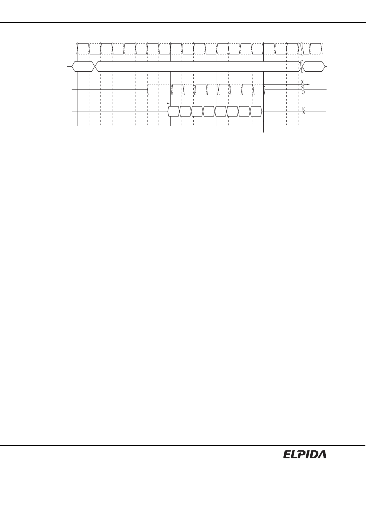
/CK
CK
Command
DQS, /DQS
EDE2104ABSE, EDE2108ABSE
T0 T1 T2 T3 T4 T5 T6 T7 T8 T9 T11
Posted
WRIT
WL = 4
NOP
≥ tWR
PRE
DQ
in0 in1 in2 in3 in4 in5 in6 in7
Completion of
the burst write
Burst Write Followed by Precharge (WL = (RL-1) = 4,BL= 8)
Preliminary Data Sheet E1196E10 (Ver. 1.0)
65

EDE2104ABSE, EDE2108ABSE
Auto-Precharge Operation
Before a new row in an active bank can be opened, the active bank must be prechar ged using either the precharge
command or the auto-precharge function. When a read or a write command is given to the DDR2 SDRAM, the /CAS
timing accepts one extra address, column address A10, to allow the active bank to automatically begin precharge at
the earliest possible moment during the burst read or write cycle. If A10 is low when the read or write Command is
issued, then normal read or write burst operation is executed and the bank remains active at the completion of the
burst sequence. If A10 is high when the Read or Write Command is issued, then the auto-precharge function is
engaged. During auto-precharge, a read Command will execute as normal with the exception that the active bank
will begin to precharge on the rising edge which is /CAS latency (CL) clock cycles before the end of the read burst.
Auto-precharge can also be implemented during Write co mmands. The precharge operation engaged by the Auto
precharge command will not begin until the last data of the burst write sequence is properly stored in the memor y
array.
This feature allows the precharge operation to be partially or completely hidden during burst read cycles (depen dent
upon /CAS latency) thus improving system performance for random data access. The /RAS lockout circuit internally
delays the Precharge operation until the array restore operation has been complete d so that the auto precharge
command may be issued with any read or write command.
Burst Read with Auto Precharge [READA]
If A10 is high when a Read Command is issued, the Read with Auto-Precharg e function is engaged. The DDR2
SDRAM starts an auto Precharge operation on the rising edge which is (AL + BL/2) cycles later from the read with
AP command when tRAS (min.) is satisfied. If tRAS (min.) is not satisfied at the edge, the start point of autoprecharge operation will be delayed until tRAS (min.) is satisfied. A new bank active (command) may be issued to
the same bank if the following two conditions are satisfied simultaneously.
(1) The /RAS precharge time (tRP) has been satisfied from the clock at which the auto precharge begins.
(2) The /RAS cycle time (tRC) from the previous bank activation has been satisfied.
T0 T1 T2 T3 T4 T5 T6 T7 Tn
/CK
CK
A10 = 1
Command
DQS, /DQS
DQ
Posted
READ
AL + BL/2
CL = 3AL = 2
RL = 5
tRC (min.)
NOP NOP
≥ tRP
out0 out2out1 out3
Auto precharge begins
ACT
Burst Read with Auto Precharge Followed by an Activation to the Same Bank (tRC limit)
(RL = 5, BL = 4 (AL = 2, CL = 3, tRTP ≤ 2tCK))
ACT
Preliminary Data Sheet E1196E10 (Ver. 1.0)
66

Command
DQS, /DQS
/CK
CK
DQ
A10 = 1
Posted
READ
EDE2104ABSE, EDE2108ABSE
T0T-1 T1 T2 T3 T4 T5 T6 T7 Tn
NOP
≥ tRAS(min.)
AL = 2
CL = 3
RL = 5
out0 out2out1 out3
tRC (min.)
≥ tRP
ACT
Auto precharge begins
Burst Read with Auto Precharge Followed by an Activation to the Same Bank (tRAS lockout case)
(RL = 5, BL = 4 (AL = 2, CL = 3))
T0 T1 T2 T3 T4 T5 T6 T7 T8
/CK
CK
A10 = 1
Command
Posted
READ
NOP
≥ tRAS(min.)
ACT
NOP
DQS, /DQS
CL = 3AL = 2
RL = 5
DQ
≥tRC
Auto precharge begins
tRP (min.)
out0 out2out1 out3
Burst Read with Auto Precharge Followed by an Activation to the Same Bank (tRP limit)
(RL = 5, BL = 4 (AL = 2, CL = 3, tRTP ≤ 2tCK))
T0 T2 T4 T6 T8 T10T1 T3 T5 T7 T9 T11
CK
/CK
A10 = 1
Command
READ ACT
≥tRAS (min.)
NOP
DQS, /DQS
AL = 2
RL = 5
DQ
CL = 3
≥tRC
≥tRP
out0 out1 out2 out3 out4 out5 out6 out7
Auto precharge begins
Burst Read with Auto Precharge Followed by an Activation to the Same Bank
(RL = 5, BL = 8 (AL = 2, CL = 3, tRTP ≤ 2tCK))
Preliminary Data Sheet E1196E10 (Ver. 1.0)
67

EDE2104ABSE, EDE2108ABSE
Burst Write with Auto-Precharge [WRITA]
If A10 is high when a write command is issued, the Write with auto-pr echarge function is engaged. The DDR2
SDRAM automatically begins precharge operation after the completion of the burst writes plus write recovery time
(tWR). The bank undergoing auto-precharge from the completion of the write burst may be reactivated if the
following two conditions are satisfied.
(1) The data-in to bank activate delay time (tWR + tRP) has been satisfied.
(2) The /RAS cycle time (tRC) from the previous bank activation has been satisfied.
T0 T1 T2 T3 T4 T5 T6 T7 Tm
/CK
CK
A10 = 1
Command
DQS, /DQS
DQ
Posted
WRIT
WL = RL –1 = 2
in1 in3
in0 in2
NOP
≥tWR
tRC (min.)
ACT
≥ tRP
Command
DQS, /DQS
Completion of the burst write
Auto precharge begins
Burst Write with Auto-Precharge (tRC Limit) (WL = 2, tWR =2)
T0 T3 T4 T5 T6 T7 T8 T9 T10 T11
/CK
CK
A10 = 1
DQ
Posted
WRIT
NOP
WL = RL –1 = 4
in0 in2
in1 in3
Completion of the burst write
NOP
tWR (min.)
≥ tRC
Auto precharge begins
tRP (min.)
Burst Write with Auto-Precharge (tWR + tRP) (WL = 4, tWR =2, tRP=3)
ACT
Preliminary Data Sheet E1196E10 (Ver. 1.0)
68

EDE2104ABSE, EDE2108ABSE
T0 T2 T4 T6 T8 T10T3 T5 T7 T9 T11 T12 T13
CK
/CK
A10 = 1
Command
DQS, /DQS
DQ
WRIT ACT
WL = RL − 1 = 4
in1 in2 in3 in4 in5 in6
in0
≥tRC
NOP
≥tWR ≥tRP
in7
Auto precharge begins
Burst Write with Auto Precharge Followed by an Activation to the Same Bank
(WL = 4, BL = 8, tWR = 2, tRP = 3)
Preliminary Data Sheet E1196E10 (Ver. 1.0)
69

EDE2104ABSE, EDE2108ABSE
Refresh Requirements
DDR2 SDRAM requires a refresh of all rows in any rolling 64ms interval. Each refresh is generated in one of t wo
ways: by an explicit automatic refresh command, or by an internally timed event in self-refresh mode . Dividing the
number of device rows into the rolling 64 ms interval defines the average r efresh interval, tREFI, which is a gu ideline
to controllers for distributed refresh timing.
Automatic Refresh Command [REF]
When /CS, /RAS and /CAS are held low and /WE high at the rising edge of the clock, the chip enters the automatic
refresh mode (REF). All banks of the DDR2 SDRAM must be precharged and idle for a minimum of the precharge
time (tRP) before the auto-refresh command (REF) can be applied. An address counter, internal to the device,
supplies the bank address during the refresh cycle. No control of the external addr ess bus is required once this
cycle has started.
When the refresh cycle has completed, all banks of the DDR2 SDRAM will be in the precharged (idle) state. A delay
between the auto-refresh command (REF) and the next activate command or subsequent auto-refresh comman d
must be greater than or equal to the auto-refresh cycle time (tRFC).
To allow for improved efficiency in scheduling and switching bet ween tasks, some flexibility in the absolute refresh
interval is provided. A maximum of 8 refresh commands can be posted to any given DDR2 SDRAM, meaning that
the maximum absolute interval between any refresh command and the next Refresh command is 9 × tREFI.
T0 T1 T2 T3
/CK
CK
CKE
Command
VIH
≥ tRP
≥ tRFC
NOPPRE
Automatic Refresh Command
≥ tRFC
REFREF NOP
Any
Command
Preliminary Data Sheet E1196E10 (Ver. 1.0)
70

EDE2104ABSE, EDE2108ABSE
Self-Refresh Command [SELF]
The DDR2 SDRAM device has a built-in timer to accommodate self-refresh operation. The self-refresh command is
defined by having /CS, /RAS, /CAS and CKE held low with /WE high at the rising edge of the clock.
ODT must be turned off before issuing self-refresh command, by either driving ODT pin low or using EMRS
command. Once the command is registered, CKE must be held low to keep the device in self-refresh mode.
When the DDR2 SDRAM has entered self-refresh mode all of the e xternal signals except CKE, are “don’t care”.
The clock is internally disabled during self-refresh operation to save po wer. The user may change the e xternal clock
frequency or halt the external clock one clock after Self-Refresh entry is registered, however, the clock must be
restarted and stable before the device can exit self-refresh operation. Once self-refresh exit command is registered,
a delay equal or longer than the tXSNR or tXSRD must be satisfied before a valid command ca n be issued to the
device. CKE must remain high for the entire self-refresh exit period tXSRD for proper o peration. NOP or deselect
commands must be registered on each positive clock edge durin g the self-refresh exit int erval. ODT should also be
turned off during tXSRD.
/CK
CK
CKE
ODT
Comand
T0 T2T1 Tm Tn
tCK
tCH tCL
tIS
Notes: 1. Device must be in the “All banks idle” state prior to entering self refresh mode.
2. ODT must be turned off tAOFD before entering self refresh mode, and can be turned on again
when tXSRD timing is satisfied.
3. tXSRD is applied for a read or a read with autoprecharge command.
4. tXSNR is applied for any command except a read or a read with autoprecharge command.
T3 T4 T5
tRP*
tAOFD
tIS
SELF
tIH
T6
tIStIS
NOP
≥ tXSNR
≥ tXSRD
NOP
NOP
Valid
Self-Refresh Command
Preliminary Data Sheet E1196E10 (Ver. 1.0)
71

EDE2104ABSE, EDE2108ABSE
Power-Down [PDEN]
Power-down is synchronously entered when CKE is registered low (along with NOP or deselect command). CKE is
not allowed to go low while mode register or extended mode register comm and time, or read or write operation is in
progress. CKE is allowed to go low while any of other operations such as row activation, precharge or autoprecharge, or auto-refresh is in progress, but power-down IDD spec will not be applied until finishing those
operations. Timing diagrams are shown in the following pages with details for entry into power-down.
The DLL should be in a locked state when power-down is entered. Otherwise DLL should be reset after exiting
power-down mode for proper read operation.
If power-down occurs when all banks are idle, this mode is referred to as precharge po wer-down; if power-down
occurs when there is a row active in any bank, this mode is referred to as active power-down. Entering power-down
deactivates the input and output buffers, excluding CK, /CK, ODT and CKE. Also the DLL is disabled upon entering
precharge power-down or slow exit active power-down, but the DLL is kept enabled during fast exit active po werdown. In power-down mode, CKE low and a stable clock signal must be maintained at the inputs of the DDR2
SDRAM, and ODT should be in a valid state but all other input signals are “Don’t Care”. CKE low must be
maintained until tCKE has been satisfied. Power-down duration is limited by 9 times tREFI of the device.
The power-down state is synchronously exited when CKE is registered high (along with a NOP or deselect
command). CKE high must be maintained until tCKE has been satisfied. A valid, executable command can be
applied with power-down exit latency, tXP, tXARD, or tXARDS, after CKE goes high. Power-down exit latency is
defined at AC Characteristics table of this data sheet.
CK
/CK
CKE
tIHtIS tIHtIS tIH tIS tIH tIHtIS
Command
VALID
Enter power-down mode
Read to Power-Down Entry
T0 Tx Tx+2 Tx+3 Tx+4 Tx+5 Tx+6T1 T2 Tx+1 Tx+7 Tx+8 Tx+9
/CK
CK
Command
CKE
DQS
/DQS
DQ
Command
CKE
DQS
/DQS
DQ
READ
VIH
T0 Tx Tx+2 Tx+3 Tx+4 Tx+5 Tx+6T1 T2 Tx+1 Tx+7 Tx+8 Tx+9
READ
VIH
NOP
AL + CL
AL + CL
tCKE min
Exit power-down mode
Power-Down
out0out1out2out
out0out1out2out3out4out5out6out
3
CKE should be kept high until the end of burst operation.
NOP
Read operation starts with a read command and
CKE should be kept high until the end of burst operation.
7
VALID
tXP, tXARD,
tXARDS
VALID
tCKE min
VALID
VIH or VIL
BL=4
BL=8
Preliminary Data Sheet E1196E10 (Ver. 1.0)
72
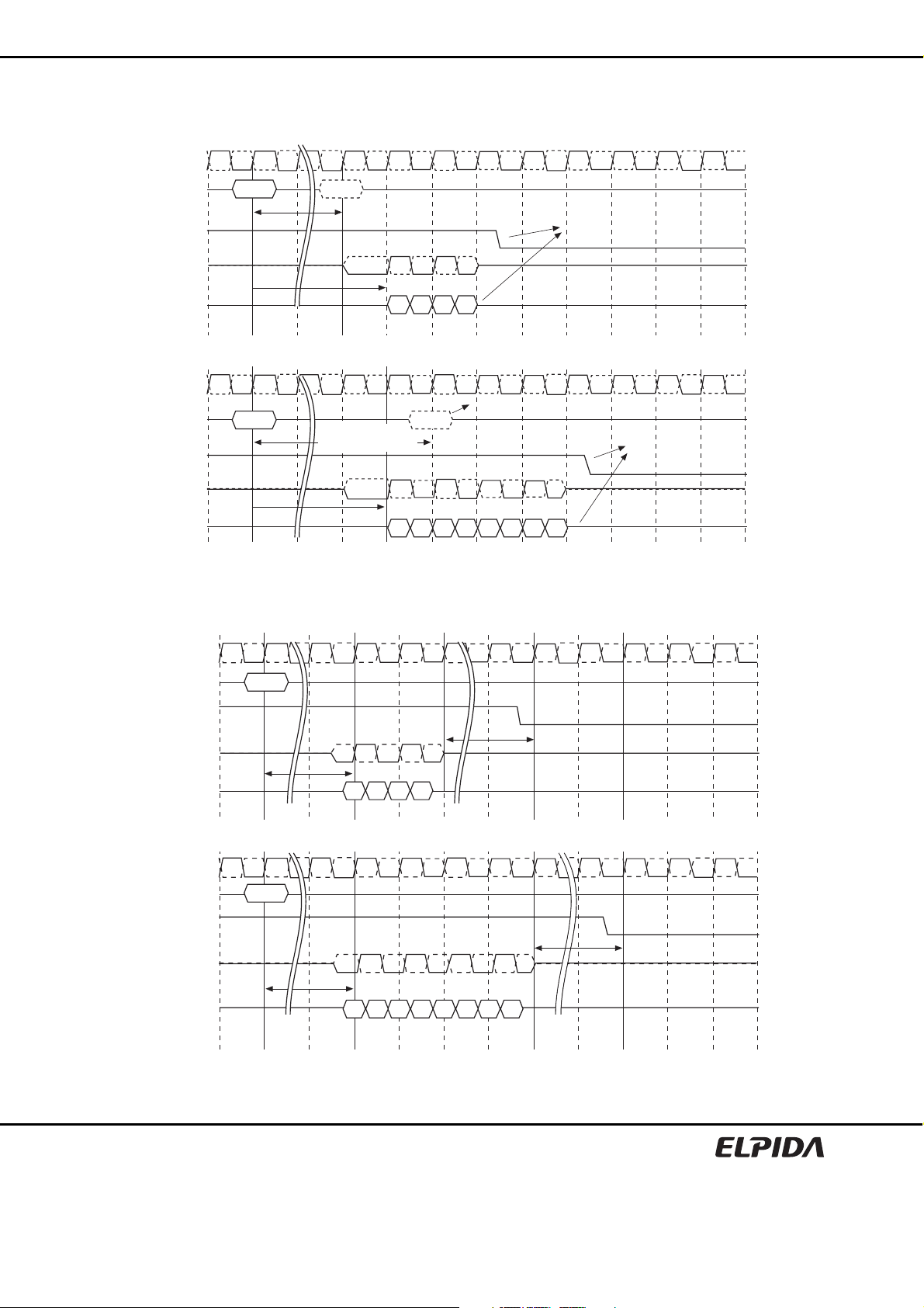
Read with Auto Precharge to Power-Down Entry
T0 Tx Tx+2 Tx+3 Tx+4 Tx+5 Tx+6T1 T2 Tx+1 Tx+7 Tx+8 Tx+9
/CK
CK
Command
CKE
DQS
/DQS
DQ
READA PRE
BL=4
AL + BL/2
with tRTP = 7.5ns
and tRAS min. satisfied
AL + CL
out0out1out2out
T0 Tx Tx+2 Tx+3 Tx+4 Tx+5 Tx+6T1 T2 Tx+1 Tx+7 Tx+8 Tx+9
EDE2104ABSE, EDE2108ABSE
CKE should be kept high
until the end of burst operation.
3
Command
READA
BL=8
CKE
DQS
/DQS
DQ
Write to Power-Down Entry
T0 Tm+1 Tm+3 Tx Tx+1 Tx+2 Tx+3T1 Tm Tm+2 Tx+4 Tx+5 Tx+6
/CK
CK
Command
CKE
DQS
/DQS
DQ
WRIT
T0 Tm+1 Tm+3 Tm+4 Tm+5 Tx Tx+1T1 Tm Tm+2 Tx+2 Tx+3 Tx+4
AL + BL/2
with tRTP = 7.5ns
and tRAS min. satisfied
AL + CL
WL
out0out1out2out
in0in1in2in
3
PRE
Start internal precharge
out4out5out6out
3
7
tWTR
CKE should be kept high
until the end of burst operation.
BL=4
Command
WRIT
CKE
DQS
tWTR
/DQS
DQ
WL
in0in1in2in3in4in5in6in
7
BL=8
Preliminary Data Sheet E1196E10 (Ver. 1.0)
73

Write with Auto Precharge to Power-Down Entry
T0 Tm+1 Tm+3 Tx Tx+1 Tx+2 Tx+3T1 Tm Tm+2 Tx+4 Tx+5 Tx+6
/CK
CK
Command
WRITA PRE
EDE2104ABSE, EDE2108ABSE
CKE
DQS
/DQS
DQ
/CK
CK
Command
CKE
DQS
/DQS
DQ
WR*1
WL
in0in1in2in
3
T0 Tm+1 Tm+3 Tm+4 Tm+5 Tx Tx+1T1 Tm Tm+2 Tx+2 Tx+3 Tx+4
WRITA
WL
in0in1in2in3in4in5in6in
7
Note: 1. WR is programmed through MRS
PRE
WR*1
BL=4
BL=8
Preliminary Data Sheet E1196E10 (Ver. 1.0)
74

Refresh Command to Power-Down Entry
EDE2104ABSE, EDE2108ABSE
T0 T3 T5 T6 T7 T8 T9T1 T2 T4 T10
/CK
CK
Command
CKE
REF
CKE can go to low one clock after an auto-refresh command
Active Command to Power-Down Entry
Command
CKE
ACT
CKE can go to low one clock after an active command
Precharge/Precharge All Command to Power-Down Entry
T11
Command
CKE
PRE or
PALL
CKE can go to low one clock after a precharge or precharge all command
MRS/EMRS Command to Power-Down Entry
Command
CKE
MRS or
EMRS
tMRD
Preliminary Data Sheet E1196E10 (Ver. 1.0)
75

EDE2104ABSE, EDE2108ABSE
Asynchronous CKE Low Event
DRAM requires CKE to be maintained high for all valid operations as defined in this data sheet. If CKE
asynchronously drops low during any valid operation DRAM is not guar anteed to preserve the contents of array. If
this event occurs, memory controller must satisfy DRAM timing specification tDELAY before turning off the clocks.
Stable clocks must exist at the input of DRAM before CKE is raised high again. DRAM must be fully re-initialized
(steps 4 through 13) as described in initialization sequence. DRAM is ready for normal operation after the
initialization sequence. See AC Characteristics table for tDELAY specification
Stable clocks
/CK
CK
CKE
tCK
tDELAY
CKE asynchronously
drops low
Clocks can be
turned off after
this point
Preliminary Data Sheet E1196E10 (Ver. 1.0)
76

EDE2104ABSE, EDE2108ABSE
Input Clock Frequency Change during Precharge Power-Down
DDR2 SDRAM input clock frequency can be changed under following condition:
DDR2 SDRAM is in precharged power-down mode. ODT must be turned off and CKE must be at lo gic low level.
A minimum of 2 clocks must be waited after CKE goes low before clock frequency may c hange. SDRAM input cl ock
frequency is allowed to change only within minimum and maximum operating frequency specified for the particular
speed grade. During input clock frequency change, ODT and CKE must be held at stable low levels.
Once input clock frequency is changed, stable new clocks must be provided to DRAM before precharge power-do wn
may be exited and DLL must be RESET via EMRS after precharge power-down exit. Depending on new clock
frequency an additional MRS command may need to be issued to appr opriately set the WR, CL and soon. During
DLL relock period, ODT must remain off. After the DLL lock time, the DRAM is ready to operate with new clock
frequency.
Clock Frequency Change in Precharge Power-Down Mode
Ty+4
Ty+3 Tz
DLL
RESET
NOP Valid
/CK
CK
Command
T0 T4 Tx+1 Ty Ty+1 Ty+2T1 T2 Tx
NOP NOP NOP NOP
CKE
ODT
tRP
tAOFD
Minmum 2 clocks
required before
changing frequency
Frequency change
occurs here
Stable new clock
before power down exit
200 clocks
tXP
ODT is off during
DLL RESET
Burst Interruption
Interruption of a burst read or write cycle is prohibited.
No Operation Command [NOP]
The no operation command should be used in cases when the DDR2 SDRAM is in an idle or a wait state. The
purpose of the no operation command is to prevent the DDR2 SDRAM from registering any unwanted commands
between operations. A no operation command is registered when /CS is low with /RAS, /CAS, and /WE held high at
the rising edge of the clock. A no operation command will not terminate a previous operation that is still executing,
such as a burst read or write cycle.
Deselect Command [DESL]
The deselect command performs the same function as a no operation command. Deselect Command occurs when
/CS is brought high at the rising edge of the clock, the /RAS, /CAS, and /WE signals become don’t cares.
Preliminary Data Sheet E1196E10 (Ver. 1.0)
77

Package Drawing
68-ball FBGA
Solder ball: Lead free (Sn-Ag-Cu)
19.0 ± 0.1
10.2 ± 0.1
INDEX MARK
EDE2104ABSE, EDE2108ABSE
Unit: mm
0.2 S B
A
0.2 S A
0.1 S
0.2
S
B
68-φ0.45 ± 0.05
1.20 max.
S
0.35 ± 0.05
0.8
14.4
φ0.15
MSA
B
INDEX MARK
1.6
0.8
6.4
Preliminary Data Sheet E1196E10 (Ver. 1.0)
ECA-TS2-0234-01
78

EDE2104ABSE, EDE2108ABSE
Recommended Soldering Conditions
Please consult with our sales offices for soldering conditions of the EDE21XXABSE.
Type of Surface Mount Device
EDE2104ABSE, EDE2108ABSE: 68-ball FBGA < Lead free (Sn-Ag-Cu) >
Preliminary Data Sheet E1196E10 (Ver. 1.0)
79

EDE2104ABSE, EDE2108ABSE
NOTES FOR CMOS DEVICES
1 PRECAUTION AGAINST ESD FOR MOS DEVICES
Exposing the MOS devices to a strong electric field can cause destruction of the gate
oxide and ultimately degrade the MOS devices operation. Steps must be taken to stop
generation of static electricity as much as possible, and quickly dissipate it, when once
it has occurred. Environmental control must be adequate. When it is dry, humidifier
should be used. It is recommended to avoid using insulators that easily build static
electricity. MOS devices must be stored and transported in an anti-static container,
static shielding bag or conductive material. All test and measurement tools including
work bench and floor should be grounded. The operator should be grounded using
wrist strap. MOS devices must not be touched with bare hands. Similar precautions
need to be taken for PW boards with semiconductor MOS devices on it.
2 HANDLING OF UNUSED INPUT PINS FOR CMOS DEVICES
No connection for CMOS devices input pins can be a cause of malfunction. If no
connection is provided to the input pins, it is possible that an internal input level may be
generated due to noise, etc., hence causing malfunction. CMOS devices behave
differently than Bipolar or NMOS devices. Input levels of CMOS devices must be fixed
high or low by using a pull-up or pull-down circuitry. Each unused pin should be connected
to V
DD
or GND with a resistor, if it is considered to have a possibility of being an output
pin. The unused pins must be handled in accordance with the related specifications.
3 STATUS BEFORE INITIALIZATION OF MOS DEVICES
Power-on does not necessarily define initial status of MOS devices. Production process
of MOS does not define the initial operation status of the device. Immediately after the
power source is turned ON, the MOS devices with reset function have not yet been
initialized. Hence, power-on does not guarantee output pin levels, I/O settings or
contents of registers. MOS devices are not initialized until the reset signal is received.
Reset operation must be executed immediately after power-on for MOS devices having
reset function.
CME0107
Preliminary Data Sheet E1196E10 (Ver. 1.0)
80

EDE2104ABSE, EDE2108ABSE
The information in this document is subject to change without notice. Before using this document, confirm that this is the latest version.
No part of this document may be copied or reproduced in any form or by any means without the prior
written consent of Elpida Memory, Inc.
Elpida Memory, Inc. does not assume any liability for infringement of any intellectual property rights
(including but not limited to patents, copyrights, and circuit layout licenses) of Elpida Memory, Inc. or
third parties by or arising from the use of the products or information listed in this document. No license,
express, implied or otherwise, is granted under any patents, copyrights or other intellectual property
rights of Elpida Memory, Inc. or others.
Descriptions of circuits, software and other related information in this document are provided for
illustrative purposes in semiconductor product operation and application examples. The incorporation of
these circuits, software and information in the design of the customer's equipment shall be done under
the full responsibility of the customer. Elpida Memory, Inc. assumes no responsibility for any losses
incurred by customers or third parties arising from the use of these circuits, software and information.
[Product applications]
Be aware that this product is for use in typical electronic equipment for general-purpose applications.
Elpida Memory, Inc. makes every attempt to ensure that its products are of high quality and reliability.
However, users are instructed to contact Elpida Memory's sales office before using the product in
aerospace, aeronautics, nuclear power, combustion control, transportation, traffic, safety equipment,
medical equipment for life support, or other such application in which especially high quality and
reliability is demanded or where its failure or malfunction may directly threaten human life or cause risk
of bodily injury.
[Product usage]
Design your application so that the product is used within the ranges and conditions guaranteed by
Elpida Memory, Inc., including the maximum ratings, operating supply voltage range, heat radiation
characteristics, installation conditions and other related characteristics. Elpida Memory, Inc. bears no
responsibility for failure or damage when the product is used beyond the guaranteed ranges and
conditions. Even within the guaranteed ranges and conditions, consider normally foreseeable failure
rates or failure modes in semiconductor devices and employ systemic measures such as fail-safes, so
that the equipment incorporating Elpida Memory, Inc. products does not cause bodily injury, fire or other
consequential damage due to the operation of the Elpida Memory, Inc. product.
[Usage environment]
Usage in environments with special characteristics as listed below was not considered in the design.
Accordingly, our company assumes no responsibility for loss of a customer or a third party when used in
environments with the special characteristics listed below.
Example:
1) Usage in liquids, including water, oils, chemicals and organic solvents.
2) Usage in exposure to direct sunlight or the outdoors, or in dusty places.
3) Usage involving exposure to significant amounts of corrosive gas, including sea air, CL
SO
, and NOx.
2
4) Usage in environments with static electricity, or strong electromagnetic waves or radiation.
5) Usage in places where dew forms.
6) Usage in environments with mechanical vibration, impact, or stress.
7) Usage near heating elements, igniters, or flammable items.
If you export the products or technology described in this document that are controlled by the Foreign
Exchange and Foreign Trade Law of Japan, you must follow the necessary procedures in accordance
with the relevant laws and regulations of Japan. Also, if you export products/technology controlled by
U.S. export control regulations, or another country's export control laws or regulations, you must follow
the necessary procedures in accordance with such laws or regulations.
If these products/technology are sold, leased, or transferred to a third party, or a third party is granted
license to use these products, that third party must be made aware that they are responsible for
compliance with the relevant laws and regulations.
, H2S, NH3,
2
M01E0706
Preliminary Data Sheet E1196E10 (Ver. 1.0)
81
 Loading...