

查询EDD5104ADTA供应商查询EDD5104ADTA供应商
EDD5104ADTA (128M words ×××× 4 bits)
EDD5108ADTA (64M words ×××× 8 bits)
EDD5116ADTA (32M words ×××× 16 bits)
DATA SHEET
512M bits DDR SDRAM
Description
The EDD5104AD, the EDD5108AD and the
EDD5116AD are 512M bits Double Data Rate (DDR)
SDRAM. Read and write operations are performed at
the cross points of the CK and the /CK. This highspeed data transfer is realized by the 2 bits prefetchpipelined architecture. Data strobe (DQS) both for
read and write are available for high speed and reliable
data bus design. By setting extended mode register,
the on-chip Delay Locked Loop (DLL) can be set
enable or disable. It is packaged in standard 66-pin
plastic TSOP (II).
Features
• Power supply: VDD, VDDQ = 2.5V ± 0.2V
• Data Rate: 333Mbps/266Mbps (max.)
• Double Data Rate architecture; two data transfers per
clock cycle
• Bi-directional, data strobe (DQS) is transmitted
/received with data, to be used in capturing data at
the receiver
• Data inputs, outputs, and DM are synchronized with
DQS
• 4 internal banks for concurrent operation
• DQS is edge aligned with data for READs; center
aligned with data for WRITEs
• Differential clock inputs (CK and /CK)
• DLL aligns DQ and DQS transitions with CK
transitions
• Commands entered on each positive CK edge; data
and data mask referenced to both edges of DQS
• Data mask (DM) for write data
• Auto precharge option for each burst access
• SSTL_2 compatible I/O
• Programmable burst length (BL): 2, 4, 8
• Programmable /CAS latency (CL): 2, 2.5
• Programmable output driver strength: normal/weak
• Refresh cycles: 8192 refresh cycles/64ms
7.8µs maximum average periodic refresh interval
• 2 variations of refresh
Auto refresh
Self refresh
Document No. E0384E30 (Ver. 3.0)
Date Published January 2004 (K) Japan
URL: http://www.elpida.com
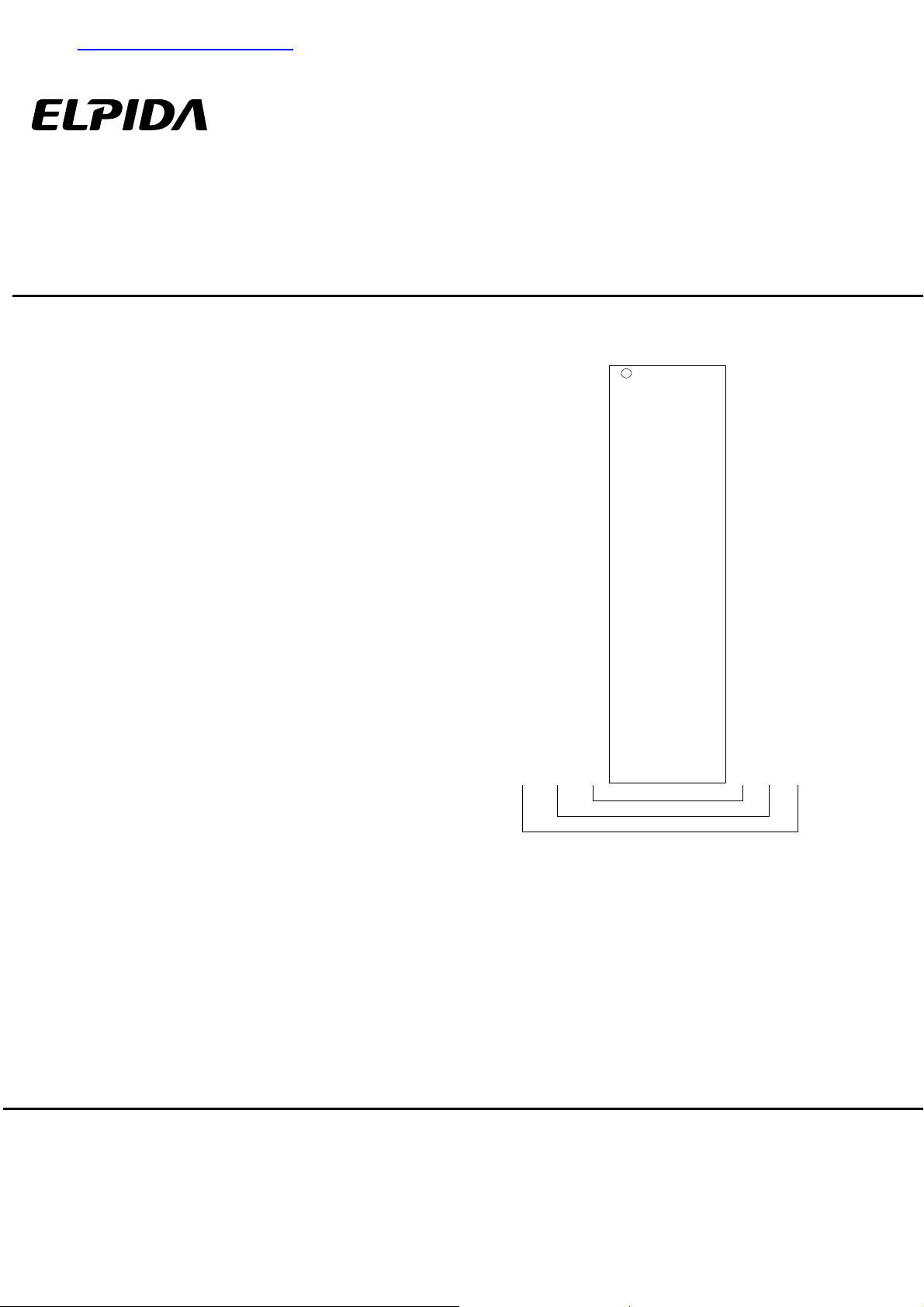
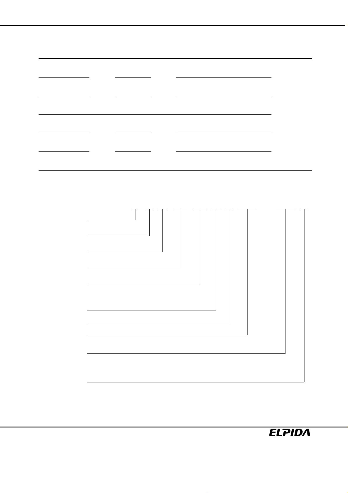
Pin Configurations
/xxx indicates active low signal.
66-pin Plastic TSOP(II)
VDD
VDD
VDD
NC
VDDQ
NC
DQ0
VSSQ
NC
NC
VDDQ
NC
DQ1
VSSQ
NC
NC
VDDQ
NC
NC
VDD
NC
NC
/WE
/CAS
/RAS
/CS
NC
BA0
BA1
A10(AP)
A0
A1
A2
A3
VDD
DQ0
VDDQ
NC
DQ1
VSSQ
NC
DQ2
VDDQ
NC
DQ3
VSSQ
NC
NC
VDDQ
NC
NC
VDD
NC
NC
/WE
/CAS
/RAS
/CS
NC
BA0
BA1
A10(AP)
A0
A1
A2
A3
VDD
A0 to A12
BA0, BA1
DQ0 to DQ15
DQS, LDQS, UDQS
/CS
/RAS
/CAS
/WE
DM, LDM, UDM
CK
/CK
CKE
VREF
VDD
VSS
VDDQ
VSSQ
NC
DQ0
VDDQ
DQ1
DQ2
VSSQ
DQ3
DQ4
VDDQ
DQ5
DQ6
VSSQ
DQ7
NC
VDDQ
LDQS
NC
VDD
NC
LDM
/WE
/CAS
/RAS
/CS
NC
BA0
BA1
A10(AP)
VDD
1
2
3
4
5
6
7
8
9
10
11
12
13
14
15
16
17
18
19
20
21
22
23
24
25
26
27
28
A0
29
A1
30
A2
31
A3
32
33
X 16
X 8
X 4
(Top view)
Address input
Bank select address
Data-input/output
Input and output data strobe
Chip select
Row address strobe command
Column address strobe command
Write enable
Input mask
Clock input
Differential clock input
Clock enable
Input reference voltage
Power for internal circuit
Ground for internal circuit
Power for DQ circuit
Ground for DQ circuit
No connection
66
VSS
65
DQ15
64
VSSQ
63
DQ14
62
DQ13
61
VDDQ
60
DQ12
59
DQ11
58
VSSQ
57
DQ10
56
DQ9
55
VDDQ
54
DQ8
53
NC
52
VSSQ
51
UDQS
50
NC
49
VREF
48
VSS
47
UDM
46
/CK
45
CK
44
CKE
43
NC
42
A12
41
A11
40
A9
39
A8
38
A7
37
A6
36
A5
35
A4
34
VSS
VSS
DQ7
VSSQ
NC
DQ6
VDDQ
NC
DQ5
VSSQ
NC
DQ4
VDDQ
NC
NC
VSSQ
DQS
NC
VREF
VSS
DM
/CK
CK
CKE
NC
A12
A11
A9
A8
A7
A6
A5
A4
VSS
VSS
NC
VSSQ
NC
DQ3
VDDQ
NC
NC
VSSQ
NC
DQ2
VDDQ
NC
NC
VSSQ
DQS
NC
VREF
VSS
DM
/CK
CK
CKE
NC
A12
A11
A9
A8
A7
A6
A5
A4
VSS
Elpida Memory, Inc. 2003-2004
Ordering Information
Part number
EDD5104ADTA-6B
EDD5104ADTA-7A
EDD5104ADTA-7B
EDD5108ADTA-6B
EDD5108ADTA-7A
EDD5108ADTA-7B
EDD5116ADTA-6B
EDD5116ADTA-7A
EDD5116ADTA-7B
EDD5104ADTA-6BL
EDD5104ADTA-7AL
EDD5104ADTA-7BL
EDD5108ADTA-6BL
EDD5108ADTA-7AL
EDD5108ADTA-7BL
EDD5116ADTA-6BL
EDD5116ADTA-7AL
EDD5116ADTA-7BL
Part Number
Mask
version
D 128M × 4 4
64M × 8
32M × 16
D 128M × 4 4
64M × 8
32M × 16
EDD5104ADTA, EDD5108ADTA, EDD5116ADTA
Organization
(words × bits)
Internal
banks
Data rate
Mbps (max.)
333
266
266
333
266
266
333
266
266
333
266
266
333
266
266
333
266
266
JEDEC speed bin
(CL-tRCD-tRP)
DDR333B (2.5-3-3)
DDR266A (2-3-3)
DDR266B (2.5-3-3)
DDR333B (2.5-3-3)
DDR266A (2-3-3)
DDR266B (2.5-3-3)
DDR333B (2.5-3-3)
DDR266A (2-3-3)
DDR266B (2.5-3-3)
DDR333B (2.5-3-3)
DDR266A (2-3-3)
DDR266B (2.5-3-3)
DDR333B (2.5-3-3)
DDR266A (2-3-3)
DDR266B (2.5-3-3)
DDR333B (2.5-3-3)
DDR266A (2-3-3)
DDR266B (2.5-3-3)
Package
66-pin Plastic
TSOP (II)
Elpida Memory
Type
D: Monolithic Device
Product Code
D: DDR SDRAM
Density / Bank
51: 512M / 4-bank
Bit Organization
04: x4
08: x8
16: x16
Voltage, Interface
A: 2.5V, SSTL_2
Die Rev.
Package
TA: TSOP (II)
Speed
6B: DDR333B (2.5-3-3)
7A: DDR266A (2-3-3)
7B: DDR266B (2.5-3-3)
E D D 51 04 A D TA - 6B L
Power Consumption
Blank: Normal
L: Low Power
Data Sheet E0384E30 (Ver. 3.0)
2

CONTENTS
EDD5104ADTA, EDD5108ADTA, EDD5116ADTA
Description.....................................................................................................................................................1
Features.........................................................................................................................................................1
Pin Configurations .........................................................................................................................................1
Ordering Information......................................................................................................................................2
Part Number ..................................................................................................................................................2
Electrical Specifications.................................................................................................................................4
Block Diagram .............................................................................................................................................10
Pin Function.................................................................................................................................................11
Command Operation ...................................................................................................................................13
Simplified State Diagram .............................................................................................................................20
Operation of the DDR SDRAM ....................................................................................................................21
Timing Waveforms.......................................................................................................................................40
Package Drawing ........................................................................................................................................46
Recommended Soldering Conditions ..........................................................................................................47
Data Sheet E0384E30 (Ver. 3.0)
3
EDD5104ADTA, EDD5108ADTA, EDD5116ADTA
Electrical Specifications
• All voltages are referenced to VSS (GND).
• After power up, wait more than 200 µs and then, execute power on sequence and CBR (Auto) refresh before
proper device operation is achieved.
Absolute Maximum Ratings
Parameter Symbol Rating Unit Note
Voltage on any pin relative to VSS VT –1.0 to +3.6 V
Supply voltage relative to VSS VDD –1.0 to +3.6 V
Short circuit output current IOS 50 mA
Power dissipation PD 1.0 W
Operating ambient temperature TA 0 to +70 °C
Storage temperature Tstg –55 to +125 °C
Caution
Exposing the device to stress above those listed in Absolute Maximum Ratings could cause
permanent damage. The device is not meant to be operated under conditions outside the limits
described in the operational section of this specification. Exposure to Absolute Maximum Rating
conditions for extended periods may affect device reliability.
Recommended DC Operating Conditions (TA = 0 to +70°°°°C)
Parameter Symbol min typ max Unit Notes
Supply voltage
Input reference voltage VREF 0.49 × VDDQ 0.50 × VDDQ 0.51 × VDDQ V
Termination voltage VTT VREF – 0.04 VREF VREF + 0.04 V
Input high voltage VIH (DC) VREF + 0.15 — VDDQ + 0.3 V 2
Input low voltage VIL (DC) –0.3 — VREF – 0.15 V 3
Input voltage level,
CK and /CK inputs
Input differential cross point
voltage, CK and /CK inputs
Input differential voltage,
CK and /CK inputs
VDD,
VDDQ
VSS,
VSSQ
VIN (DC) –0.3 — VDDQ + 0.3 V 4
VIX (DC) 0.5 × VDDQ − 0.2V 0.5 × VDDQ 0.5 × VDDQ + 0.2V V
VID (DC) 0.36 — VDDQ + 0.6 V 5, 6
2.3 2.5 2.7 V 1
0 0 0 V
Notes: 1. VDDQ must be lower than or equal to VDD.
2. VIH is allowed to exceed VDD up to 3.6V for the period shorter than or equal to 5ns.
3. VIL is allowed to outreach below VSS down to –1.0V for the period shorter than or equal to 5ns.
4. VIN (DC) specifies the allowable DC execution of each differential input.
5. VID (DC) specifies the input differential voltage required for switching.
6. VIH (CK) min assumed over VREF + 0.18V, VIL (CK) max assumed under VREF – 0.18V
if measurement.
Data Sheet E0384E30 (Ver. 3.0)
4
EDD5104ADTA, EDD5108ADTA, EDD5116ADTA
DC Characteristics 1 (TA = 0 to +70°°°°C, VDD, VDDQ = 2.5V ± 0.2V, VSS, VSSQ = 0V)
max.
Parameter Symbol Grade × 4 × 8 × 16 Unit Test condition Notes
Operating current (ACTPRE)
Operating current
(ACT-READ-PRE)
Idle power down standby
current
Floating idle standby
current
Quiet idle standby current IDD2Q 20 20 20 mA
Active power down
standby current
Active standby current IDD3N
Operating current
(Burst read operation)
Operating current
(Burst write operation)
Auto Refresh current IDD5
Self refresh current IDD6 4 4 4 mA
Self refresh current
((L-version))
Operating current
(4 banks interleaving)
IDD0
IDD1
IDD2P 3 3 3 mA CKE ≤ VIL 4
IDD2F
IDD3P 20 20 20 mA CKE ≤ VIL 3
IDD4R
IDD4W
IDD6 -xxL 3 3 3 mA
IDD7A
Notes: 1. These IDD data are measured under condition that DQ pins are not connected.
2. One bank operation.
3. One bank active.
4. All banks idle.
5. Command/Address transition once per one clock cycle.
6. DQ, DM and DQS transition twice per one clock cycle.
7. 4 banks active. Only one bank is running at tRC = tRC (min.)
8. The IDD data on this table are measured with regard to tCK = tCK (min.) in general.
9. Command/Address transition once every two clock cycles.
10. Command/Address stable at ≥ VIH or ≤ VIL.
-6B
-7A, -7B
-6B
-7A, -7B
-6B
-7A, -7B
-6B
-7A, -7B
-6B
-7A, -7B
-6B
-7A, -7B
-6B
-7A, -7B
-6B
-7A, -7B
150
135
190
170
30
25
65
55
230
200
230
200
320
300
490
410
150
135
200
175
30
25
65
55
250
210
250
210
320
300
510
430
150
135
210
180
30
25
65
55
270
230
270
230
320
300
530
450
CKE ≥ VIH,
mA
tRC = tRC (min.)
CKE ≥ VIH, BL = 4,
mA
CL = 2.5,
tRC = tRC (min.)
CKE ≥ VIH, /CS ≥ VIH,
mA
DQ, DQS, DM = VREF
CKE ≥ VIH, /CS ≥ VIH,
DQ, DQS, DM = VREF
CKE ≥ VIH, /CS ≥ VIH
mA
tRAS = tRAS (max.)
CKE ≥ VIH, BL = 2,
mA
CL = 2.5
CKE ≥ VIH, BL = 2,
mA
CL = 2.5
tRFC = tRFC (min.),
mA
Input ≤ VIL or ≥ VIH
Input ≥ VDD – 0.2 V
Input ≤ 0.2 V
mA BL = 4 1, 5, 6, 7
1, 2, 9
1, 2, 5
4, 5
4, 10
3, 5, 6
1, 2, 5, 6
1, 2, 5, 6
DC Characteristics 2 (TA = 0 to +70°°°°C, VDD, VDDQ = 2.5V ± 0.2V, VSS, VSSQ = 0V)
Parameter Symbol min. max. Unit Test condition Notes
Input leakage current ILI –2 2 µA VDD ≥ VIN ≥ VSS
Output leakage current ILO –5 5 µA VDDQ ≥ VOUT ≥ VSS
Output high current IOH –15.2 — mA VOUT = 1.95V
Output low current IOL 15.2 — mA VOUT = 0.35V
Data Sheet E0384E30 (Ver. 3.0)
5
EDD5104ADTA, EDD5108ADTA, EDD5116ADTA
Pin Capacitance (TA = +25°C, VDD, VDDQ = 2.5V ± 0.2V)
Parameter Symbol Pins min. typ max. Unit Notes
Input capacitance CI1 CK, /CK 2.0 — 3.0 pF 1
CI2 All other input pins 2.0 — 3.0 pF 1
Delta input capacitance Cdi1 CK, /CK — — 0.25 pF 1
Cdi2 All other input-only pins — — 0.5 pF 1
Data input/output capacitance CI/O DQ, DM, DQS 4.0 — 5 pF 1, 2,
Delta input/output capacitance Cdio DQ, DM, DQS — — 0.5 pF 1
Notes: 1. These parameters are measured on conditions: f = 100MHz, VOUT = VDDQ/2, ∆VOUT = 0.2V,
TA = +25°C.
2. DOUT circuits are disabled.
AC Characteristics (TA = 0 to +70°°°°C, VDD, VDDQ = 2.5V ± 0.2V, VSS, VSSQ = 0V)
-6B -7A -7B
Parameter Symbol
Clock cycle time
(CL = 2)
(CL = 2.5) tCK 6 12 7.5 12 7.5 12 ns
CK high-level width tCH 0.45 0.55 0.45 0.55 0.45 0.55 tCK
CK low-level width tCL 0.45 0.55 0.45 0.55 0.45 0.55 tCK
CK half period tHP
DQ output access time from CK, /CK tAC –0.7 0.7 –0.75 0.75 –0.75 0.75 ns 2, 11
DQS output access time from CK,
/CK
DQS to DQ skew tDQSQ — 0.45 — 0.5 — 0.5 ns 3
DQ/DQS output hold time from DQS tQH tHP – tQHS — tHP – tQHS — tHP – tQHS — ns
Data hold skew factor tQHS — 0.55 — 0.75 — 0.75 ns
Data-out high-impedance time from
CK, /CK
Data-out low-impedance time from
CK, /CK
Read preamble tRPRE 0.9 1.1 0.9 1.1 0.9 1.1 tCK
Read postamble tRPST 0.4 0.6 0.4 0.6 0.4 0.6 tCK
DQ and DM input setup time tDS 0.45 — 0.5 — 0.5 — ns 8
DQ and DM input hold time tDH 0.45 — 0.5 — 0.5 — ns 8
DQ and DM input pulse width tDIPW 1.75 — 1.75 — 1.75 — ns 7
Write preamble setup time tWPRES 0 — 0 — 0 — ns
Write preamble tWPRE 0.25 — 0.25 — 0.25 — tCK
Write postamble tWPST 0.4 0.6 0.4 0.6 0.4 0.6 tCK 9
Write command to first DQS latching
transition
DQS falling edge to CK setup time tDSS 0.2 — 0.2 — 0.2 — tCK
DQS falling edge hold time from CK tDSH 0.2 — 0.2 — 0.2 — tCK
DQS input high pulse width tDQSH 0.35 — 0.35 — 0.35 — tCK
DQS input low pulse width tDQSL 0.35 0.35 — 0.35 — tCK
tCK 7.5 12 7.5 12 10 12 ns 10
tDQSCK –0.6 0.6 –0.75 0.75 –0.75 0.75 ns 2, 11
tHZ –0.7 0.7 –0.75 0.75 –0.75 0.75 ns 5, 11
tLZ –0.7 0.7 –0.75 0.75 –0.75 0.75 ns 6, 11
tDQSS 0.75 1.25 0.75 1.25 0.75 1.25 tCK
min. max. min. max min. max.
min
(tCH, tCL)
—
min
(tCH, tCL)
—
min
(tCH, tCL)
— tCK
Unit Notes
Address and control input setup time tIS 0.75 — 0.9 — 0.9 — ns 8
Address and control input hold time tIH 0.75 — 0.9 — 0.9 — ns 8
Data Sheet E0384E30 (Ver. 3.0)
6
EDD5104ADTA, EDD5108ADTA, EDD5116ADTA
-6B -7A -7B
Parameter Symbol
Address and control input pulse width tIPW 2.2 — 2.2 — 2.2 — ns 7
Mode register set command cycle
time
Active to Precharge command period tRAS 42 120000 45 120000 45 120000 ns
Active to Active/Auto refresh
command period
Auto refresh to Active/Auto refresh
command period
Active to Read/Write delay tRCD 18 — 20 — 20 — ns
Precharge to active command period tRP 18 — 20 — 20 — ns
Active to Autoprecharge delay tRAP tRCD min. — tRCD min. — tRCD min. — ns
Active to active command period tRRD 12 — 15 — 15 — ns
Write recovery time tWR 15 — 15 — 15 — ns
Auto precharge write recovery and
precharge time
Internal write to Read command
delay
Average periodic refresh interval tREF — 7.8 — 7.8 — 7.8 µs
tMRD 2 — 2 — 2 — tCK
tRC 60 — 65 — 65 — ns
tRFC 72 — 75 — 75 — ns
tDAL
tWTR 1 — 1 — 1 — tCK
Notes: 1. On all AC measurements, we assume the test conditions shown in the next page. For timing parameter
definitions, see ‘Timing Waveforms’ section.
2. This parameter defines the signal transition delay from the cross point of CK and /CK. The signal
transition is defined to occur when the signal level crossing VTT.
3. The timing reference level is VTT.
4. Output valid window is defined to be the period between two successive transition of data out or DQS
(read) signals. The signal transition is defined to occur when the signal level crossing VTT.
5. tHZ is defined as DOUT transition delay from Low-Z to High-Z at the end of read burst operation. The
timing reference is cross point of CK and /CK. This parameter is not referred to a specific DOUT voltage
level, but specify when the device output stops driving.
6. tLZ is defined as DOUT transition delay from High-Z to Low-Z at the beginning of read operation. This
parameter is not referred to a specific DOUT voltage level, but specify when the device output begins
driving.
7. Input valid windows is defined to be the period between two successive transition of data input or DQS
(write) signals. The signal transition is defined to occur when the signal level crossing VREF.
8. The timing reference level is VREF.
9. The transition from Low-Z to High-Z is defined to occur when the device output stops driving. A specific
reference voltage to judge this transition is not given.
10. tCK (max.) is determined by the lock range of the DLL. Beyond this lock range, the DLL operation is not
assured.
11. tCK = tCK (min.) when these parameters are measured. Otherwise, absolute minimum values of these
values are 10% of tCK.
12. VDD is assumed to be 2.5V ± 0.2V. VDD power supply variation per cycle expected to be less than
0.4V/400 cycle.
13. tDAL = (tWR/tCK)+(tRP/tCK)
For each of the terms above, if not already an integer, round to the next highest integer.
Example: For –7A Speed at CL = 2.5, tCK = 7.5ns, tWR = 15ns and tRP= 20ns,
tDAL = (15ns/7.5ns) + (20ns/7.5ns) = (2) + (3)
tDAL = 5 clocks
min. max. min. max min. max.
(tWR/tCK)+
(tRP/tCK)
(tWR/tCK)+
(tRP/tCK)
—
(tWR/tCK)+
(tRP/tCK)
— tCK 13
Unit Notes
Data Sheet E0384E30 (Ver. 3.0)
7
EDD5104ADTA, EDD5108ADTA, EDD5116ADTA
Test Conditions
Parameter Symbol Value Unit
Input reference voltage VREF VDDQ/2 V
Termination voltage VTT VREF V
Input high voltage VIH (AC) VREF + 0.31 V
Input low voltage VIL (AC) VREF − 0.31 V
Input differential voltage, CK and /CK
inputs
Input differential cross point voltage,
CK and /CK inputs
Input signal slew rate SLEW 1 V/ns
CK
/CK
VID (AC) 0.62 V
VIX (AC) VREF V
VID
tCL
tCK
tCH
VDD
VREF
VSS
VIX
VDD
VIH
VIL
∆t
SLEW = (VIH (AC) – VIL (AC))/∆t
VTT
Measurement point
RT = 50Ω
DQ
CL = 30pF
Input Waveforms and Output Load
VREF
VSS
Data Sheet E0384E30 (Ver. 3.0)
8
EDD5104ADTA, EDD5108ADTA, EDD5116ADTA
Timing Parameter Measured in Clock Cycle
Number of clock cycle
tCK 6ns 7.5ns
Parameter Symbol min. max. min. max. Unit
Write to pre-charge command delay (same bank) tWPD 4 + BL/2 — 3 + BL/2 — tCK
Read to pre-charge command delay (same bank) tRPD BL/2 — BL/2 — tCK
Write to read command delay (to input all data) tWRD 2 + BL/2 — 2 + BL/2 — tCK
Burst stop command to write command delay
(CL = 2)
(CL = 2.5) tBSTW 3 — 3 — tCK
Burst stop command to DQ High-Z
(CL = 2)
(CL = 2.5) tBSTZ 2.5 2.5 2.5 2.5 tCK
Read command to write command delay
(to output all data)
(CL = 2)
(CL = 2.5) tRWD 3 + BL/2 — 3 + B L/2 — tCK
Pre-charge command to High-Z
(CL = 2)
(CL = 2.5) tHZP 2.5 2.5 2.5 2.5 tCK
Write command to data in latency tWCD 1 1 1 1 tCK
Write recovery time tWR 3 — 2 — tCK
DM to data in latency tDMD 0 0 0 0 tCK
Mode register set command cycle time tMRD 2 — 2 — tCK
Self refresh exit to non-read command tSNR 12 — 10 — tCK
Self refresh exit to read command tSRD 200 — 200 — tCK
Power down entry tPDEN 1 1 1 1 tCK
Power down exit to command input tPDEX 1 — 1 — tCK
tBSTW — — 2 — tCK
tBSTZ — — 2 2 tCK
tRWD — — 2 + BL/2 — tCK
tHZP — — 2 2 tCK
Data Sheet E0384E30 (Ver. 3.0)
9
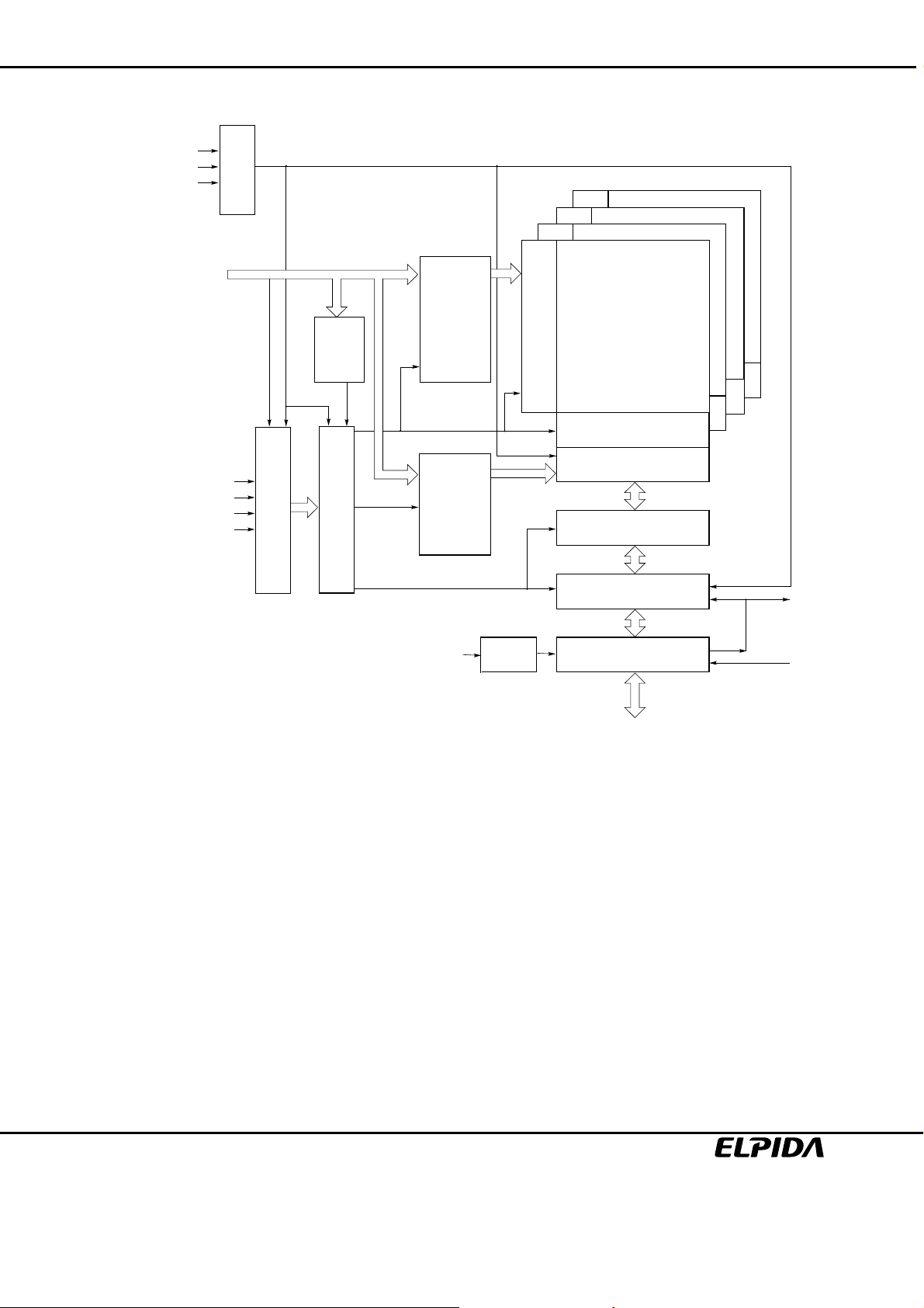
Block Diagram
CK
/CK
CKE
Clock
generator
EDD5104ADTA, EDD5108ADTA, EDD5116ADTA
Bank 3
Bank 2
Bank 1
A0 to A12, BA0, BA1
/RAS
/CAS
/CS
/WE
Mode
register
Control logic
Command decoder
Row
address
buffer
and
refresh
counter
Column
address
buffer
and
burst
counter
CK, /CK
DLL
Memory cell array
Row decoder
Sense amp.
Column decoder
Data control circuit
Latch circuit
Input & Output buffer
Bank 0
DQS
DM
DQ
Data Sheet E0384E30 (Ver. 3.0)
10
EDD5104ADTA, EDD5108ADTA, EDD5116ADTA
Pin Function
CK, /CK (input pins)
The CK and the /CK are the master clock inputs. All inputs except DM, DQS and DQs are referred to the cross point
of the CK rising edge and the /CK falling edge. When a read operation, DQS and DQs are referred to the cross point
of the CK and the /CK. When a write operation, DQS and DQs are referred to the cross point of the DQS and the
VREF level. DQS for write operation is referred to the cross point of the CK and the /CK. CK is the master clock
input to this pin. The other input signals are referred at CK rising edge.
/CS (input pin)
When /CS is Low, commands and data can be input. When /CS is High, all inputs are ignored. However, internal
operations (bank active, burst operations, etc.) are held.
/RAS, /CAS, and /WE (input pins)
These pins define operating commands (read, write, etc.) depending on the combinations of their voltage levels.
See "Command operation".
A0 to A12 (input pins)
Row address (AX0 to AX12) is determined by the A0 to the A12 level at the cross point of the CK rising edge and the
/CK falling edge in a bank active command cycle. Column address (See “Address Pins Table”) is loaded via the A0
to the A9, A11 and A12 at the cross point of the CK rising edge and the /CK falling edge in a read or a write
command cycle. This column address becomes the starting address of a burst operation.
[Address Pins Table]
Address (A0 to A12)
Part number Row address Column address
EDD5104AD AX0 to AX12 AY0 to AY9, AY11, AY12
EDD5108AD AX0 to AX12 AY0 to AY9, AY11
EDD5116AD AX0 to AX12 AY0 to AY9
A10 (AP) (input pin)
A10 defines the precharge mode when a precharge command, a read command or a write command is issued. If
A10 = High when a precharge command is issued, all banks are precharged. If A10 = Low when a precharge
command is issued, only the bank that is selected by BA1/BA0 is precharged. If A10 = High when read or write
command, auto-precharge function is enabled. While A10 = Low, auto-precharge function is disabled.
BA0 and BA1 (input pins)
BA0, BA1 are bank select signals (BA). The memory array is divided into bank 0, bank 1, bank 2 and bank 3. (See
Bank Select Signal Table)
[Bank Select Signal Table]
BA0 BA1
Bank 0 L L
Bank 1 H L
Bank 2 L H
Bank 3 H H
Remark: H: VIH. L: VIL
Data Sheet E0384E30 (Ver. 3.0)
11

EDD5104ADTA, EDD5108ADTA, EDD5116ADTA
CKE (input pin)
This pin determines whether or not the next CK is valid. If CKE is High, the next CK rising edge is valid. If CKE is
Low. CKE controls power down and self-refresh. The power down and the self-refresh commands are entered when
the CKE is driven Low and exited when it resumes to High. CKE must be maintained high throughout read or write
access.
The CKE level must be kept for 1 CK cycle at least, that is, if CKE changes at the cross point of the CK rising edge
and the /CK falling edge with proper setup time tIS, by the next CK rising edge CKE level must be kept with proper
hold time tIH.
DM, LDM and UDM (input pins)
DMs are the reference signal of the data input mask function. DMs are sampled at the cross point of DQS and
VREF. DMs provide the byte mask function. When DM = High, the data input at the same timing are masked while
the internal burst counter will be count up. In ×16 products, LDM controls the lower byte (DQ0 to DQ7) and UDM
controls the upper byte (DQ8 to DQ15) of write data.
DQ0 to DQ15 (input/output pins)
Data is input to and output from these pins (DQ0 to DQ3; EDD5104AD, DQ0 to DQ7; EDD5108AD, DQ0 to DQ15;
EDD5116AD).
DQS, LDQS and UDQS (input and output pins)
DQS provides the read data strobes (as output) and the write data strobes (as input). In ×16 products, LDQS is the
lower byte (DQ0 to DQ7) data strobe signal, UDQS is the upper byte (DQ8 to DQ15) data strobe signal.
VDD, VSS, VDDQ, VSSQ (Power supply)
VDD and VSS are power supply pins for internal circuits. VDDQ and VSSQ are power supply pins for the output
buffers.
Data Sheet E0384E30 (Ver. 3.0)
12
EDD5104ADTA, EDD5108ADTA, EDD5116ADTA
Command Operation
Command Truth Table
DDR SDRAM recognize the following commands specified by the /CS, /RAS, /CAS, /WE and address pins. All other
combinations than those in the table below are illegal.
CKE
Command Symbol n – 1 n /CS /RAS /CAS /WE BA1 BA0 AP Address
Ignore command DESL H H H × × × × × × ×
No operation NOP H H L H H H × × × ×
Burst stop in read command BST H H L H H L × × × ×
Column address and read command READ H H L H L H V V L V
Read with auto-precharge READA H H L H L H V V H V
Column address and write command WRIT H H L H L L V V L V
Write with auto-precharge WRITA H H L H L L V V H V
Row address strobe and bank active ACT H H L L H H V V V V
Precharge select bank PRE H H L L H L V V L ×
Precharge all bank PALL H H L L H L × × H ×
Refresh REF H H L L L H × × × ×
SELF H L L L L H × × × ×
Mode register set MRS H H L L L L L L L V
EMRS H H L L L L L H L V
Remark: H: VIH. L: VIL. ×: VIH or VIL V: Valid address input
Note: The CKE level must be kept for 1 CK cycle at least.
Ignore command [DESL]
When /CS is High at the cross point of the CK rising edge and the VREF level, every input are neglected and internal
status is held.
No operation [NOP]
As long as this command is input at the cross point of the CK rising edge and the VREF level, address and data
input are neglected and internal status is held.
Burst stop in read operation [BST]
This command stops a burst read operation, which is not applicable for a burst write operation.
Column address strobe and read command [READ]
This command starts a read operation. The start address of the burst read is determined by the column address
(See “Address Pins Table” in Pin Function) and the bank select address. After the completion of the read operation,
the output buffer becomes High-Z.
Read with auto-precharge [READA]
This command starts a read operation. After completion of the read operation, precharge is automatically executed.
Column address strobe and write command [WRIT]
This command starts a write operation. The start address of the burst write is determined by the column address
(See “Address Pins Table” in Pin Function) and the bank select address.
Write with auto-precharge [WRITA]
This command starts a write operation. After completion of the write operation, precharge is automatically executed.
Data Sheet E0384E30 (Ver. 3.0)
13
EDD5104ADTA, EDD5108ADTA, EDD5116ADTA
Row address strobe and bank activate [ACT]
This command activates the bank that is selected by BA0, BA1 and determines the row address (AX0 to AX12).
(See Bank Select Signal Table)
Precharge selected bank [PRE]
This command starts precharge operation for the bank selected by BA0, BA1. (See Bank Select Signal Table)
[Bank Select Signal Table]
BA0 BA1
Bank 0 L L
Bank 1 H L
Bank 2 L H
Bank 3 H H
Remark: H: VIH. L: VIL
Precharge all banks [PALL]
This command starts a precharge operation for all banks.
Refresh [REF/SELF]
This command starts a refresh operation. There are two types of refresh operation, one is auto-refresh, and another
is self-refresh. For details, refer to the CKE truth table section.
Mode register set/Extended mode register set [MRS/EMRS]
The DDR SDRAM has the two mode registers, the mode register and the extended mode register, to defines how it
works. The both mode registers are set through the address pins (the A0 to the A12, BA0 to BA1) in the mode
register set cycle. For details, refer to "Mode register and extended mode register set".
CKE Truth Table
CKE
Current state Command n – 1 n /CS /RAS /CAS /WE Address Notes
Idle Auto-refresh command (REF) H H L L L H × 2
Idle Self-refresh entry (SELF) H L L L L H × 1, 2
Idle Power down entry (PDEN) H L L H H H ×
H L H × × × ×
Self refresh Self refresh exit (SELFX) L H L H H H ×
L H H × × × ×
Power down Power down exit (PDEX) L H L H H H ×
L H H × × × ×
Remark: H: VIH. L: VIL. ×: VIH or VIL.
Notes: 1. All the banks must be in IDLE before executing this command.
2. The CKE level must be kept for 1 CK cycle at least.
Data Sheet E0384E30 (Ver. 3.0)
14
EDD5104ADTA, EDD5108ADTA, EDD5116ADTA
Function Truth Table
The following tables show the operations that are performed when each command is issued in each state of the
DDR SDRAM.
Current state /CS /RAS /CAS /WE Address Command Operation Next state
1
Precharging*
L H H H × NOP NOP ldle
L H H L × BST ILLEGAL*
L H L H BA, CA, A10 READ/READA ILLEGAL*11 —
L H L L BA, CA, A10 WRIT/WRITA ILLEGAL*11 —
L L H H BA, RA ACT ILLEGAL*11 —
L L H L BA, A10 PRE, PALL NOP ldle
L L L × × ILLEGAL —
2
Idle*
H × × × × DESL NOP ldle
L H H H × NOP NOP ldle
L H H L × BST ILLEGAL*
L H L H BA, CA, A10 READ/READA ILLEGAL*11 —
L H L L BA, CA, A10 WRIT/WRITA ILLEGAL*11 —
L L H H BA, RA ACT Activating Active
L L H L BA, A10 PRE, PALL NOP ldle
L L L H × REF, SELF
L L L L MODE MRS Mode register set*12 ldle
Refresh
(auto-refresh)*
L H H H × NOP NOP ldle
L H H L × BST ILLEGAL —
L H L × × ILLEGAL —
L L × × × ILLEGAL —
Activating*
L H H H × NOP NOP Active
L H H L × BST ILLEGAL*
L H L H BA, CA, A10 READ/READA ILLEGAL*11 —
L H L L BA, CA, A10 WRIT/WRITA ILLEGAL*11 —
L L H H BA, RA ACT ILLEGAL*11 —
L L H L BA, A10 PRE, PALL ILLEGAL*11 —
L L L × × ILLEGAL —
Active*
L H H H × NOP NOP Active
L H H L × BST ILLEGAL Active
L H L H BA, CA, A10 READ/READA Starting read operation Read/READA
L H L L BA, CA, A10 WRIT/WRITA Starting write operation
L L H H BA, RA ACT ILLEGAL*11 —
L L H L BA, A10 PRE, PALL Pre-charge Idle
L L L × × ILLEGAL —
H × × × × DESL NOP ldle
11
—
11
—
Refresh/
Self refresh*
H × × × × DESL NOP ldle
3
4
H × × × × DESL NOP Active
5
H × × × × DESL NOP Active
12
11
—
ldle/
Self refresh
Write
recovering/
precharging
Data Sheet E0384E30 (Ver. 3.0)
15

EDD5104ADTA, EDD5108ADTA, EDD5116ADTA
Current state /CS /RAS /CAS /WE Address Command Operation Next state
6
H × × × × DESL NOP Active
Read*
L H H H × NOP NOP Active
L H H L × BST BST Active
L H L H BA, CA, A10 READ/READA
L H L L BA, CA, A10 WRIT/WRITA ILLEGAL*13 —
L L H H BA, RA ACT ILLEGAL*11 —
L L H L BA, A10 PRE, PALL
L L L × × ILLEGAL —
Read with auto-pre-
7
charge*
H × × × × DESL NOP Precharging
L H H H × NOP NOP Precharging
L H H L × BST ILLEGAL —
L H L H BA, CA, A10 READ/READA ILLEGAL*14 —
L H L L BA, CA, A10 WRIT/WRITA ILLEGAL*14 —
L L H H BA, RA ACT ILLEGAL*
L L H L BA, A10 PRE, PALL ILLEGAL*
L L L × × ILLEGAL —
8
Write*
H × × × × DESL NOP
L H H H × NOP NOP
L H H L × BST ILLEGAL —
L H L H BA, CA, A10 READ/READA
L H L L BA, CA, A10 WRIT/WRITA
L L H H BA, RA ACT ILLEGAL*11 —
L L H L BA, A10 PRE, PALL
L L L × × ILLEGAL —
Write recovering*
9
H × × × × DESL NOP Active
L H H H × NOP NOP Active
L H H L × BST ILLEGAL —
L H L H BA, CA, A10 READ/READA Starting read operation. Read/ReadA
L H L L BA, CA, A10 WRIT/WRITA
L L H H BA, RA ACT ILLEGAL*11 —
L L H L BA, A10 PRE/PALL ILLEGAL*11 —
L L L × × ILLEGAL —
Interrupting burst read
operation to
start new read
Interrupting burst
read operation to
start pre-charge
11, 14
—
11, 14
—
Interrupting burst write
operation to
start read operation.
Interrupting burst write
operation to
start new write
operation.
Interrupting write
operation to start precharge.
Starting new write
operation.
Active
Precharging
Write
recovering
Write
recovering
Read/ReadA
Write/WriteA
Idle
Write/WriteA
Data Sheet E0384E30 (Ver. 3.0)
16

EDD5104ADTA, EDD5108ADTA, EDD5116ADTA
Current state /CS /RAS /CAS /WE Address Command Operation Next state
Write with autopre-charge*10
L H H H × NOP NOP Precharging
L H H L × BST ILLEGAL —
L H L H BA, CA, A10 READ/READA ILLEGAL*14 —
L H L L BA, CA, A10 WRIT/WRIT A ILLEGAL*14 —
L L H H BA, RA ACT ILLEGAL*
L L H L BA, A10 PRE, PALL ILLEGAL*
L L L × × ILLEGAL —
Remark: H: VIH. L: VIL. ×: VIH or VIL
Notes: 1. The DDR SDRAM is in "Precharging" state for tRP after precharge command is issued.
2. The DDR SDRAM reaches "IDLE" state tRP after precharge command is issued.
3. The DDR SDRAM is in "Refresh" state for tRFC after auto-refresh command is issued.
4. The DDR SDRAM is in "Activating" state for tRCD after ACT command is issued.
5. The DDR SDRAM is in "Active" state after "Activating" is completed.
6. The DDR SDRAM is in "READ" state until burst data have been output and DQ output circuits are turned
off.
7. The DDR SDRAM is in "READ with auto-precharge" from READA command until burst data has been
output and DQ output circuits are turned off.
8. The DDR SDRAM is in "WRITE" state from WRIT command to the last burst data are input.
9. The DDR SDRAM is in "Write recovering" for tWR after the last data are input.
10. The DDR SDRAM is in "Write with auto-precharge" until tWR after the last data has been input.
11. This command may be issued for other banks, depending on the state of the banks.
12. All banks must be in "IDLE".
13. Before executing a write command to stop the preceding burst read operation, BST command must be
issued.
14.The DDR SDRAM supports the concurrent auto-precharge feature, a read with auto-precharge enabled,or
a write with auto-precharge enabled, may be followed by any column command to other banks, as long as
that command does not interrupt the read or write data transfer, and all other related limitations apply.
(E.g. Conflict between READ data and WRITE data must be avoided.)
From command
Read w/AP Read or Read w/AP BL/2 tCK
Write or Write w/AP CL(rounded up)+ (BL/2) tCK
Precharge or Activate 1 tCK
Write w/AP Read or Read w/AP 1 + (BL/2) + tWTR tCK
Write or Write w/AP BL/2 tCK
Precharge or Activate 1 tCK
H × × × × DESL NOP Precharging
11, 14
—
11, 14
—
The minimum delay from a read or write command with auto precharge enabled, to a command to a
different bank, is summarized below.
To command (different bank, noninterrupting command)
Minimum delay
(Concurrent AP supported)
Units
Data Sheet E0384E30 (Ver. 3.0)
17

EDD5104ADTA, EDD5108ADTA, EDD5116ADTA
Command Truth Table for CKE
Current State CKE
n – 1 n /CS /RAS /CAS /WE Address Operation Notes
Self refresh H × × × × × × INVALID, CK (n-1) would exit self refresh
L H H × × × × Self refresh recovery
L H L H H × × Self refresh recovery
L H L H L × × ILLEGAL
L H L L × × × ILLEGAL
L L × × × × × Maintain self refresh
Self refresh recovery H H H × × × × Idle after tRC
H H L H H × × Idle after tRC
H H L H L × × ILLEGAL
H H L L × × × ILLEGAL
H L H × × × × ILLEGAL
H L L H H × × ILLEGAL
H L L H L × × ILLEGAL
H L L L × × × ILLEGAL
Power down H × × × × × INVALID, CK (n – 1) would exit power down
L H H × × × × EXIT power down → Idle
L H L H H H ×
L L × × × × × Maintain power down mode
All banks idle H H H × × × Refer to operations in Function Truth Table
H H L H × × Refer to operations in Function Truth Table
H H L L H × Refer to operations in Function Truth Table
H H L L L H × CBR (auto) refresh
H H L L L L OPCODE Refer to operations in Function Truth Table
H L H × × × Refer to operations in Function Truth Table
H L L H × × Refer to operations in Function Truth Table
H L L L H × Refer to operations in Function Truth Table
H L L L L H × Self refresh 1
H L L L L L OPCODE Refer to operations in Function Truth Table
L × × × × × × Power down 1
Row active H × × × × × × Refer to operations in Function Truth Table
L × × × × × × Power down 1
Remark: H: VIH. L: VIL. ×: VIH or VIL
Note: Self refresh can be entered only from the all banks idle state. Power down can be entered only from all
banks idle or row active state.
Data Sheet E0384E30 (Ver. 3.0)
18

EDD5104ADTA, EDD5108ADTA, EDD5116ADTA
Auto-refresh command [REF]
This command executes auto-refresh. The banks and the ROW addresses to be refreshed are internally determined
by the internal refresh controller. The average refresh cycle is 7.8 µs. The output buffer becomes High-Z after auto-
refresh start. Precharge has been completed automatically after the auto-refresh. The ACT or MRS command can
be issued tRFC
Self-refresh entry [SELF]
This command starts self-refresh. The self-refresh operation continues as long as CKE is held Low. During the selfrefresh operation, all ROW addresses are repeated refreshing by the internal refresh controller. A self-refresh is
terminated by a self-refresh exit command.
Power down mode entry [PDEN]
tPDEN (= 1 cycle) after the cycle when [PDEN] is issued. The DDR SDRAM enters into power-down mode. In
power down mode, power consumption is suppressed by deactivating the input initial circuit. Power down mode
continues while CKE is held Low. No internal refresh operation occurs during the power down mode. [PDEN] do not
disable DLL.
Self-refresh exit [SELFX]
This command is executed to exit from self-refresh mode. To issue non-read commands, tSNR has to be satisfied.
((tSNR =)10 cycles for tCK = 7.5 ns or 12 cycles for tCK = 6.0 ns after [SELFX]) To issue read command, tSRD has
to be satisfied to adjust DOUT timing by DLL. (200 cycles after [SELFX]) After the exit, input auto-refresh command
within 7.8 µs.
Power down exit [PDEX]
The DDR SDRAM can exit from power down mode tPDEX (1 cycle min.) after the cycle when [PDEX] is issued.
after the last auto-refresh command.
Data Sheet E0384E30 (Ver. 3.0)
19

Simplified State Diagram
EDD5104ADTA, EDD5108ADTA, EDD5116ADTA
SELF
REFRESH
SR ENTRY
SR EXIT
POWER
APPLIED
MODE
REGISTER
SET
ACTIVE
POWER
DOWN
Write
WRITE
WITH AP
POWER
ON
MRS
CKE_
CKE
WRITE
WRITE
WRITEA READA
PRECHARGE PRECHARGE
PRECHARGE
ROW
ACTIVE
WRITE
WITH
AP
READ
READ
WITH AP
PRECHARGE
PRECHARGE
IDLE
ACTIVE
READ
WITH
AP
REFRESH
CKE_
CKE
BST
READ
IDLE
POWER
DOWN
READ
AUTO
REFRESH
Read
READ
WITH AP
*1
Automatic transition after completion of command.
Transition resulting from command input.
Note: 1. After the auto-refresh operation, precharge operation is performed automatically
and enter the IDLE state.
Data Sheet E0384E30 (Ver. 3.0)
20

EDD5104ADTA, EDD5108ADTA, EDD5116ADTA
Operation of the DDR SDRAM
Power-up Sequence
(1) Apply power and maintain CKE at an LVCMOS low state (all other inputs are undefined).
Apply VDD before or at the same time as VDDQ.
Apply VDDQ before or at the same time as VTT and VREF.
(2) Start clock and maintain stable condition for a minimum of 200 µs.
(3) After the minimum 200 µs of stable power and clock (CK, /CK), apply NOP and take CKE high.
(4) Issue precharge all command for the device.
(5) Issue EMRS to enable DLL.
(6) Issue a mode register set command (MRS) for "DLL reset" with bit A8 set to high (An additional 200 cycles of
clock input is required to lock the DLL after every DLL reset).
(7) Issue precharge all command for the device.
(8) Issue 2 or more auto-refresh commands.
(9) Issue a mode register set command to initialize device operation with bit A8 set to low in order to avoid resetting
the DLL.
/CK
CK
Command
(4) (5) (6) (7)
PALL MRS REF
2 cycles (min.) 2 cycles (min.)
EMRS
DLL enable
PALL MRS
DLL reset with A8 = High
t
RP
Power-up Sequence after CKE Goes High
(8) (9)
REF
t
RFC
200 cycles (min)
REF
t
RFC
Disable DLL reset with A8 = Low
Any
command
2 cycles (min.)2 cycles (min.)
Mode Register and Extended Mode Register Set
There are two mode registers, the mode register and the extended mode register so as to define the operating
mode. Parameters are set to both through the A0 to the A12 and BA0, BA1 pins by the mode register set command
[MRS] or the extended mode register set command [EMRS]. The mode register and the extended mode register are
set by inputting signal via the A0 to the A12 and BA0, BA1 during mode register set cycles. BA0 and BA1 determine
which one of the mode register or the extended mode register are set. Prior to a read or a write operation, the mode
register must be set.
Remind that no other parameters shown in the table bellow are allowed to input to the registers.
BA0
0
A11 A10A12BA1
0
A9 A8 A7 A6 A5 A4 A3 A2 A1 A0
0000 0DR LMODE BT BL
MRS
A8
DLL Reset
0No
1 Yes
A6 A5 A4 CAS Latency
010
110
2
2.5
A3
Burst Type
0 Sequential
1 Interleave
A2 A1 A0
001
010
Burst Length
BT=0 BT=1
2
4
011 8
2
4
8
Mode Register Set [MRS] (BA0 = 0, BA1 = 0)
Data Sheet E0384E30 (Ver. 3.0)
21

EDD5104ADTA, EDD5108ADTA, EDD5116ADTA
BA0
0
1
EMRS
Burst Operation
The burst type (BT) and the first three bits of the column address determine the order of a data out.
Burst length = 2
Starting Ad.
A0
0
1
Burst length = 8
Starting Ad.
A2 A1 A0
000
001
010
011
100
101
110
111
A11 A10A12BA1
Extended Mode Register Set [EMRS] (BA0 = 1, BA1 = 0)
Addressing(decimal)
0, 1,
1, 0,
Addressing(decimal)
0, 1, 2, 3, 4, 5, 6, 7,
1, 2, 3, 4, 5, 6, 7,
2, 3, 4, 5, 6, 7,
3, 4, 5, 6, 7,
4, 5, 6, 7,
5, 6, 7,
6, 7,
7,
A9 A8 A7 A6 A5 A4 A3 A2 A1 A0
000 0 0000 0 0 DS DLL0
A1
Driver Strength
0 Normal
1 Weak
Burst length = 4
Starting Ad.
InterleaveSequence
0, 1,
1, 0,
0, 1, 2, 3,
0, 1, 2, 3, 4,
0, 1, 2, 3, 4, 5,
0, 1, 2, 3, 4, 5, 6,
A1 A0
0, 1,
0, 1, 2,
00
01
10
11
0,
Addressing(decimal)
0, 1, 2, 3,
1, 2, 3, 0,
2, 3, 0, 1,
3,
0, 1, 2,
InterleaveSequence
0, 1, 2, 3, 4, 5, 6, 7,
1, 0, 3, 2, 5, 4, 7,
2, 3, 0, 1, 6, 7,
3, 2, 1, 0, 7,
4, 5, 6, 7,
5, 4, 7,
6, 7,
7,
6, 5, 4, 3, 2, 1, 0,
0, 1, 2, 3,
6, 1, 0, 3, 2,
4, 5, 2, 3, 0, 1,
A0
0 DLL Enable
1 DLL Disable
InterleaveSequence
4, 5,
6, 5, 4,
DLL Control
0, 1, 2, 3,
1, 0, 3, 2,
2, 3, 0, 1,
3, 2, 1, 0,
6,
Data Sheet E0384E30 (Ver. 3.0)
22

EDD5104ADTA, EDD5108ADTA, EDD5116ADTA
Read/Write Operations
Bank active
A read or a write operation begins with the bank active command [ACT]. The bank active command determines a
bank address and a row address. For the bank and the row, a read or a write command can be issued tRCD after
the ACT is issued.
Read operation
The burst length (BL), the /CAS latency (CL) and the burst type (BT) of the mode register are referred when a read
command is issued. The burst length (BL) determines the length of a sequential output data by the read command
that can be set to 2, 4, or 8. The starting address of the burst read is defined by the column address, the bank select
address which are loaded via the A0 to A12 and BA0, BA1 pins in the cycle when the read command is issued. The
data output timing are characterized by CL and tAC. The read burst start CL • tCK + tAC (ns) after the clock rising
edge where the read command are latched. The DDR SDRAM output the data strobe through DQS simultaneously
with data. tRPRE prior to the first rising edge of the data strobe, the DQS are driven Low from VTT level. This low
period of DQS is referred as read preamble. The burst data are output coincidentally at both the rising and falling
edge of the data strobe. The DQ pins become High-Z in the next cycle after the burst read operation completed.
tRPST from the last falling edge of the data strobe, the DQS pins become High-Z. This low period of DQS is
referred as read postamble.
t1t0 t5t4 t6 t7 t8 t9
CK
/CK
tRCD
Command
Address
DQS
DQ
ACTNOP NOP NOPREAD
Row
BL = 2
BL = 4
BL = 8
Column
Read Operation (Burst Length)
tRPRE
out0 out1
tRPST
out0 out1 out2 out3
out0 out1 out2 out3 out4 out5 out6 out7
CL = 2
BL: Burst length
Data Sheet E0384E30 (Ver. 3.0)
23

EDD5104ADTA, EDD5108ADTA, EDD5116ADTA
t0 t0.5 t1 t1.5 t2 t2.5 t3 t3.5 t4 t4.5 t5 t5.5
CK
/CK
Command
DQS
CL = 2
DQ
DQS
CL = 2.5
DQ
READ NOP
tRPRE
tAC,tDQSCK
out0 out1 out2 out3
tRPRE
tAC,tDQSCK
out0 out1 out2 out3
tRPST
VTT
VTT
tRPST
VTT
VTT
Read Operation (/CAS Latency)
Write operation
The burst length (BL) and the burst type (BT) of the mode register are referred when a write command is issued.
The burst length (BL) determines the length of a sequential data input by the write command that can be set to 2, 4,
or 8. The latency from write command to data input is fixed to 1. The starting address of the burst read is defined by
the column address, the bank select address which are loaded via the A0 to A12, BA0 to BA1 pins in the cycle when
the write command is issued. DQS should be input as the strobe for the input-data and DM as well during burst
operation. tWPRE prior to the first rising edge of the DQS should be set to Low and tWPST after the last falling edge
of the data strobe can be set to High-Z. The leading low period of DQS is referred as write preamble. The last low
period of DQS is referred as write postamble.
t1t0 tn
tn+0.5 tn+1 tn+2 tn+3 tn+4 tn+5
CK
/CK
Command
Address
DQS
DQ
tRCD
ACTNOP NOP NOPWRITE
Row
BL = 2
BL = 4
BL = 8
Column
tWPRES
tWPRE
in1
in0
in0 in1 in2 in3
in0 in1 in2 in3 in4 in5 in6 in7
tWPST
Write Operation
BL: Burst length
Data Sheet E0384E30 (Ver. 3.0)
24

EDD5104ADTA, EDD5108ADTA, EDD5116ADTA
Burst Stop
Burst stop command during burst read
The burst stop (BST) command is used to stop data output during a burst read. The BST command stops the burst
read and sets the output buffer to High-Z. tBSTZ (= CL) cycles after a BST command issued, the DQ pins become
High-Z. The BST command is not supported for the burst write operation. Note that bank address is not referred
when this command is executed.
t0 t0.5 t1 t1.5 t2 t2.5 t3 t3.5 t4 t4.5 t5 t5.5
CK
/CK
Command
CL = 2
CL = 2.5
DQS
DQ
DQS
DQ
READ
BST NOP
tBSTZ
out0 out1
tBSTZ
2 cycles
out0 out1
Burst Stop during a Read Operation
2.5 cycles
CL: /CAS latency
Data Sheet E0384E30 (Ver. 3.0)
25

EDD5104ADTA, EDD5108ADTA, EDD5116ADTA
Auto Precharge
Read with auto-precharge
The precharge is automatically performed after completing a read operation. The precharge starts tRPD (BL/2)
cycle after READA command input. tRAP specification for READA allows a read command with auto precharge to be
issued to a bank that has been activated (opened) but has not yet satisfied the tRAS (min) specification. A column
command to the other active bank can be issued the next cycle after the last data output. Read with auto-precharge
command does not limit row commands execution for other bank. Refer to ‘Function truth table and related notes
(Notes.*14)‘.
CK
/CK
tRAP (min) = tRCD (min)
Command
DQS
DQ
Note: Internal auto-precharge starts at the timing indicated by " ".
READAACT
tRPD
2 cycles (= BL/2)
tAC,tDQSCK
NOP
out0 out1 out2 out3
tRP (min)
ACT
Read with auto-precharge
Write with auto-precharge
The precharge is automatically performed after completing a burst write operation. The precharge operation is
started (BL/ 2 + 3) cycles after WRITA command issued. A column command to the other banks can be issued the
next cycle after the internal precharge command issued. Write with auto-precharge command does not limit row
commands execution for other bank. Refer to ‘Function truth table and related notes (Notes.*14)‘.
CK
/CK
Command
tRAS (min)
tRCD (min)
ACT WRITA ACT
NOPNOP
tRP
BL/2 + 3 cycles
DM
DQS
DQ
Note: Internal auto-precharge starts at the timing indicated by " ".
in1 in2 in3 in4
BL = 4
Burst Write (BL = 4)
Data Sheet E0384E30 (Ver. 3.0)
26

EDD5104ADTA, EDD5108ADTA, EDD5116ADTA
Command Intervals
A Read command to the consecutive Read command Interval
Destination row of the
consecutive read command
Bank
address
1. Same Same ACTIVE
2. Same Different —
3. Different Any ACTIVE
IDLE
Row address State Operation
t0 t4 t5 t6 t7 t8 t9t3
CK
/CK
The consecutive read can be performed after an interval of no less than 1 cycle to
interrupt the preceding read operation.
Precharge the bank to interrupt the preceding read operation. tRP after the
precharge command, issue the ACT command. tRCD after the ACT command, the
consecutive read command can be issued. See ‘A read command to the
consecutive precharge interval’ section.
The consecutive read can be performed after an interval of no less than 1 cycle to
interrupt the preceding read operation.
Precharge the bank without interrupting the preceding read operation. tRP after
the precharge command, issue the ACT command. tRCD after the ACT command,
the consecutive read command can be issued.
Command
Address
BA
DQ
DQS
ACT NOP READ
Row Column A
Column = A
Read
Bank0
Active
READ
Column B
Column = B
Read
outA0outA1outB0outB1outB2out
Column = A
Dout
NOP
B3
Column = B
Dout
READ to READ Command Interval (same ROW address in the same bank)
CL = 2
BL = 4
Bank0
Data Sheet E0384E30 (Ver. 3.0)
27

EDD5104ADTA, EDD5108ADTA, EDD5116ADTA
t1t0 t2 t3 t4 t5 t6 t7 t8
CK
/CK
t9
Command
Address
BA
DQ
DQS
ACT NOP NOP
Row0
Bank0
Active
ACT
Row1 Column A
Bank3
Active
READ to READ Command Interval (different bank)
READ
Column = A
Read
Bank0
Read
READ
Column B
Column = B
Read
Bank3
Read
NOP
outA0outA1outB0outB1outB2out
Bank0
Dout
Bank3
Dout
B3
CL = 2
BL = 4
Data Sheet E0384E30 (Ver. 3.0)
28

EDD5104ADTA, EDD5108ADTA, EDD5116ADTA
A Write command to the consecutive Write command Interval
Destination row of the consecutive write
command
Bank
address
1. Same Same ACTIVE
2. Same Different —
3. Different Any ACTIVE
IDLE
Row address State Operation
t0 tn+1tn tn+2 tn+3 tn+4 tn+5 tn+6
CK
/CK
The consecutive write can be performed after an interval of no less than 1 cycle to
interrupt the preceding write operation.
Precharge the bank to interrupt the preceding write operation. tRP after the
precharge command, issue the ACT command. tRCD after the ACT command, the
consecutive write command can be issued. See ‘A write command to the
consecutive precharge interval’ section.
The consecutive write can be performed after an interval of no less than 1 cycle to
interrupt the preceding write operation.
Precharge the bank without interrupting the preceding write operation. tRP after
the precharge command, issue the ACT command. tRCD after the ACT command,
the consecutive write command can be issued.
Command
Address
BA
DQ
DQS
ACT NOP WRIT
Row Column A
Bank0
Active
WRIT
Column B
inA0 inA1 inB0 inB1 inB2 inB3
Column = A
Write
Column = B
Write
NOP
WRITE to WRITE Command Interval (same ROW address in the same bank)
BL = 4
Bank0
Data Sheet E0384E30 (Ver. 3.0)
29

EDD5104ADTA, EDD5108ADTA, EDD5116ADTA
t1t0 t2 tn tn+1 tn+2 tn+3 tn+4 tn+5
CK
/CK
Command
Address
BA
DQ
DQS
ACT NOP ACT
Row0 Row1 Column A
Bank0
Active
Bank3
Active
NOP WRIT
WRIT
WRITE to WRITE Command Interval (different bank)
Column B
inA0 inA1 inB0 inB1 inB2 inB3
Bank0
Write
Bank3
Write
NOP
BL = 4
Bank0, 3
Data Sheet E0384E30 (Ver. 3.0)
30

EDD5104ADTA, EDD5108ADTA, EDD5116ADTA
A Read command to the consecutive Write command interval with the BST command
Destination row of the consecutive write
command
Bank
address
1. Same Same ACTIVE
2. Same Different —
3. Different Any ACTIVE
IDLE
Row address State Operation
t1t0 t2 t3 t4 t5 t6 t7 t8
CK
/CK
Issue the BST command. tBSTW (≥ tBSTZ) after the BST command, the
consecutive write command can be issued.
Precharge the bank to interrupt the preceding read operation. tRP after the
precharge command, issue the ACT command. tRCD after the ACT command, the
consecutive write command can be issued. See ‘A read command to the
consecutive precharge interval’ section.
Issue the BST command. tBSTW (≥ tBSTZ) after the BST command, the
consecutive write command can be issued.
Precharge the bank independently of the preceding read operation. tRP after the
precharge command, issue the ACT command. tRCD after the ACT command, the
consecutive write command can be issued.
Command
DM
DQ
DQS
READ WRIT
High-Z
BST NOP NOP
tBSTW (≥ tBSTZ)
tBSTZ (= CL)
out0 out1
OUTPUT INPUT
READ to WRITE Command Interval
in0 in1
in2 in3
BL = 4
CL = 2
Data Sheet E0384E30 (Ver. 3.0)
31

EDD5104ADTA, EDD5108ADTA, EDD5116ADTA
A Write command to the consecutive Read command interval: To complete the burst operation
Destination row of the consecutive read
command
Bank
address
1. Same Same ACTIVE
2. Same Different —
3. Different Any ACTIVE
IDLE
CK
/CK
Row address State Operation
t1t0 t2 t3 t4 t5 t6
To complete the burst operation, the consecutive read command should be
performed tWRD (= BL/ 2 + 2) after the write command.
Precharge the bank tWRD after the preceding write command. tRP after the
precharge command, issue the ACT command. tRCD after the ACT command, the
consecutive read command can be issued. See ‘A read command to the
consecutive precharge interval’ section.
To complete a burst operation, the consecutive read command should be
performed tWRD (= BL/ 2 + 2) after the write command.
Precharge the bank independently of the preceding write operation. tRP after the
precharge command, issue the ACT command. tRCD after the ACT command, the
consecutive read command can be issued.
Command
DM
DQ
DQS
WRIT NOP NOPREAD
tWRD (min)
BL/2 + 2 cycle
in0 in1 in2 in3
INPUT OUTPUT
tWTR*
Note: tWTR is referenced from the first positive CK edge after the last desired data in pair tWTR.
WRITE to READ Command Interval
out0 out1
out2
BL = 4
CL = 2
Data Sheet E0384E30 (Ver. 3.0)
32

EDD5104ADTA, EDD5108ADTA, EDD5116ADTA
A Write command to the consecutive Read command interval: To interrupt the write operation
Destination row of the consecutive read
command
Bank
address
1. Same Same ACTIVE
2. Same Different — —*1
3. Different Any ACTIVE
IDLE —*
Row address State Operation
Note: 1. Precharge must be preceded to read command. Therefore read command can not interrupt the write
operation in this case.
WRITE to READ Command Interval (Same bank, same ROW address)
t1t0 t2 t3 t4 t5 t6 t7 t8
CK
/CK
DM must be input 1 cycle prior to the read command input to prevent from being
written invalid data. In case, the read command is input in the next cycle of the
write command, DM is not necessary.
DM must be input 1 cycle prior to the read command input to prevent from being
written invalid data. In case, the read command is input in the next cycle of the
write command, DM is not necessary.
1
Command
DM
DQ
DQS
1 cycle
READ NOPWRIT
in0 in1
Data masked
CL=2
in2
out0 out1
out2 out3
[WRITE to READ delay = 1 clock cycle]
High-Z
High-Z
BL = 4
CL= 2
Data Sheet E0384E30 (Ver. 3.0)
33

EDD5104ADTA, EDD5108ADTA, EDD5116ADTA
t1t0 t2 t3 t4 t5 t6 t7 t8
CK
/CK
Command
Command
DM
DQ
DQS
CK
/CK
READ NOPNOPWRIT
2 cycle
in0 in1
Data masked
in2 in3
CL=2
out0 out1
out2 out3
High-Z
High-Z
[WRITE to READ delay = 2 clock cycle]
t1t0 t2 t3 t4 t5 t6 t7 t8
READWRIT NOP NOP
BL = 4
CL= 2
DM
DQ
DQS
in0 in1
3 cycle
tWTR*
in2 in3
Data masked
CL=2
out0 out1
out2 out3
Note: tWTR is referenced from the first positive CK edge after the last desired data in pair tWTR.
[WRITE to READ delay = 3 clock cycle]
BL = 4
CL= 2
Data Sheet E0384E30 (Ver. 3.0)
34

EDD5104ADTA, EDD5108ADTA, EDD5116ADTA
A Read command to the consecutive Precharge command interval (same bank): To output all data
To complete a burst read operation and get a burst length of data, the consecutive precharge command must be
issued tRPD (= BL/ 2 cycles) after the read command is issued.
t1t0 t2 t3 t4 t5 t6 t7 t8
CK
/CK
Command
Command
PRE/
PALL
out0 out1 out2 out3
DQ
DQS
READ
NOPNOP NOP
tRPD = BL/2
READ to PRECHARGE Command Interval (same bank): To output all data (CL = 2, BL = 4)
t1t0 t2 t3 t4 t5 t6 t7 t8
CK
/CK
PRE/
PALL
out0 out1 out2 out3
DQ
DQS
READ
NOP NOP NOP
tRPD = BL/2
READ to PRECHARGE Command Interval (same bank): To output all data (CL = 2.5, BL = 4)
Data Sheet E0384E30 (Ver. 3.0)
35

EDD5104ADTA, EDD5108ADTA, EDD5116ADTA
READ to PRECHARGE Command Interval (same bank): To stop output data
A burst data output can be interrupted with a precharge command. All DQ pins and DQS pins become High-Z tHZP
(= CL) after the precharge command.
t1t0 t2 t3 t4 t5 t6 t7 t8
CK
/CK
Command
DQ
DQS
NOP NOP
READ
PRE/PALL
out0 out1
tHZP
High-Z
High-Z
READ to PRECHARGE Command Interval (same bank): To stop output data (CL = 2, BL = 2, 4, 8)
t1t0 t2 t3 t4 t5 t6 t7 t8
CK
/CK
Command
DQ
DQS
NOP NOP
READ
PRE/PALL
CL = 2.5
out0 out1
High-Z
High-Z
tHZP
READ to PRECHARGE Command Interval (same bank): To stop output data (CL = 2.5, BL = 2, 4, 8)
Data Sheet E0384E30 (Ver. 3.0)
36

EDD5104ADTA, EDD5108ADTA, EDD5116ADTA
A Write command to the consecutive Precharge command interval (same bank)
The minimum interval tWPD is necessary between the write command and the precharge command.
t1t0 t2 t3 t4 t5 t6 t7
CK
/CK
Command
DM
DQS
DQ
WRIT NOP NOP
tWPD
tWR
in0 in1 in2 in3
Last data input
PRE/PALL
WRITE to PRECHARGE Command Interval (same bank) (BL = 4)
Precharge Termination in Write Cycles
During a burst write cycle without auto precharge, the burst write operation is terminated by a precharge command
of the same bank. In order to write the last input data, tWR (min) must be satisfied. When the precharge command
is issued, the invalid data must be masked by DM.
t1t0 t2 t3 t4 t5 t6 t7
CK
/CK
Command
DM
DQS
DQ
WRIT NOP NOP
tWR
in0 in1
in2 in3
Data masked
PRE/PALL
Precharge Termination in Write Cycles (same bank) (BL = 4)
Data Sheet E0384E30 (Ver. 3.0)
37

EDD5104ADTA, EDD5108ADTA, EDD5116ADTA
Bank active command interval
Destination row of the consecutive ACT
command
Bank
address
1. Same Any ACTIVE
2. Different Any ACTIVE
IDLE tRRD after an ACT command, the next ACT command can be issued.
Row address
State
CK
/CK
Operation
Two successive ACT commands can be issued at tRC interval. In between two
successive ACT operations, precharge command should be executed.
Precharge the bank. tRP after the precharge command, the consecutive ACT
command can be issued.
Command
Address
BA
ACTV
Bank0
Active
tRRD
ROW: 1ROW: 0
Bank3
Active
tRC
PRE ACT
Bank0
Precharge
NOP NOPNOPACTACT
ROW: 0
Bank0
Active
Bank Active to Bank Active
Mode register set to Bank-active command interval
The interval between setting the mode register and executing a bank-active command must be no less than tMRD.
CK
/CK
Command
Address
CODE BS and ROW
NOP NOPMRS ACT
Mode Register Set Bank3
tMRD
Active
Data Sheet E0384E30 (Ver. 3.0)
38

EDD5104ADTA, EDD5108ADTA, EDD5116ADTA
DM Control
DM can mask input data. In ×16 products, UDM and LDM can mask the upper and lower byte of input data
respectively. By setting DM to Low, data can be written. When DM is set to High, the corresponding data is not
written, and the previous data is held. The latency between DM input and enabling/disabling mask function is 0.
t1 t2 t3 t4 t5 t6
DQS
DQ
DM
Mask Mask
Write mask latency = 0
DM Control
Data Sheet E0384E30 (Ver. 3.0)
39

EDD5104ADTA, EDD5108ADTA, EDD5116ADTA
Timing Waveforms
Command and Addresses Input Timing Definition
CK
/CK
Command
(/RAS, /CAS,
/WE, /CS)
tIS
tIS
tIH
tIH
VREF
Address
Read Timing Definition
/CK
CK
DQS
DQ
(Dout)
Write Timing Definition
/CK
CK
DQS
tWPRES
tCH
tDQSS
tCK
tRPRE
tCK
tWPRE
tCL
tDQSCK tDQSCK tDQSCK
tLZ
tDQSQ
tAC
tQH
tDQSL tDQSH tWPST
tQH
tAC
tDQSQ
tDSH tDSStDSS
tDQSCK
tDQSQ
tAC
tQH
tRPST
tQH
tHZ
VREF
tDQSQ
VREF
DQ
(Din)
tDS tDH
DM
tDS tDH
Data Sheet E0384E30 (Ver. 3.0)
tDIPW
tDIPW tDIPW
VREF
VREF
40

Read Cycle
CK
/CK
CKE
/CS
/RAS
/CAS
/WE
BA
VIH
tCH
tIS tIH
tIS tIH
tIS tIH
tIS tIH
tIS tIH
tIS tIH
tCK
tCL
tRCD
EDD5104ADTA, EDD5108ADTA, EDD5116ADTA
tRC
tIS tIH
tIS tIH
tIS tIH
tIS tIH
tIS tIH
tIS tIH
tRAS
tIS tIH
tIS tIH
tIS tIH
tIS tIH
tIS tIH
tIS
tIH
tRP
tIS tIH
tIS tIH
tIS tIH
tIS tIH
tIS tIH
tIS tIH
A10
Address
DM
DQS
DQ (output)
tIS tIH
Bank 0
Bank 0
Active
Active
High-Z
High-Z
tIS tIH
Bank 0
Bank 0
Read
Read
tRPRE
Bank 0
Precharge
tRPST
tIS tIH
CL = 2
BL = 4
Bank0 Access
= VIH or VIL
Data Sheet E0384E30 (Ver. 3.0)
41

Write Cycle
CK
/CK
CKE
/CS
VIH
tCH
tIS tIH
tCK
tCL
tRCD
EDD5104ADTA, EDD5108ADTA, EDD5116ADTA
tRC
tIS tIH
tRAS
tIS tIH
tRP
tIS tIH
/RAS
/CAS
/WE
BA
A10
Address
DQS
(input)
DM
tIS tIH
tIS tIH
tIS tIH
tIS tIH
tIS tIH
tIS tIH
tIS tIH
tIS tIH
tIS tIH
tIS tIH
tIS tIH
tIS tIH
tDS
tDS
tDQSH
tIS tIH
tIS tIH
tIS tIH
tIS
tIH
tIS tIH
tDQSL tWPSTtDQSS
tDS
tDH
tDH
tIS tIH
tIS tIH
tIS tIH
tIS tIH
tIS tIH
tIS tIH
DQ (input)
tDH
Bank 0
Bank 0
Active
Active
Data Sheet E0384E30 (Ver. 3.0)
Bank 0
Write
tWR
Bank 0
Precharge
CL = 2
BL = 4
Bank0 Access
= VIH or VIL
42

Mode Register Set Cycle
/CK
CK
CKE
/CS
/RAS
/CAS
/WE
0 1 2 3 4 5 6 7 8 9 10 11 12 13 14 15
VIH
EDD5104ADTA, EDD5108ADTA, EDD5116ADTA
BA
Address
DM
DQS
DQ (output)
Read/Write Cycle
/CK
CK
CKE
/CS
/RAS
/CAS
/WE
Address
VIH
BA
DM
valid
High-Z
High-Z
Precharge
If needed
R:a
tRP
C:a
code
code
Mode
register
set
tMRD
R: b
Bank 3
Active
C: b
Bank 3
Read
C:bR:b
b
Bank 3
Precharge
CL = 2
BL = 4
= VIH or VIL
C:b''
DQS
DQ (output)
DQ (input)
Bank 0
Active
Data Sheet E0384E30 (Ver. 3.0)
High-Z
Bank 0
Read
Bank 3
Active
a
tRWD
Bank 3
Write
b
tWRD
Bank 3
Read
b’’
Read cycle
CL = 2
BL = 4
=VIH or VIL
43
Auto Refresh Cycle
/CK
CK
CKE
/CS
/RAS
/CAS
/WE
BA
VIH
EDD5104ADTA, EDD5108ADTA, EDD5116ADTA
Address
DM
DQS
DQ (output)
DQ (input)
A10=1
Precharge
If needed
tRP
High-Z
Auto
Refresh
tRFC
R: b C: b
Bank 0
Active
Bank 0
Read
b
CL = 2
BL = 4
= VIH or VIL
Data Sheet E0384E30 (Ver. 3.0)
44

Self Refresh Cycle
/CK
CK
CKE
/CS
/RAS
/CAS
/WE
BA
EDD5104ADTA, EDD5108ADTA, EDD5116ADTA
tIS tIH
CKE = low
Address
DM
DQS
DQ (output)
DQ (input)
A10=1
Precharge
If needed
tRP
Self
refresh
entry
High-Z
Self refresh
exit
tSNR
tSRD
Bank 0
Active
R: b C: b
Bank 0
Read
CL = 2.5
BL = 4
= VIH or VIL
Data Sheet E0384E30 (Ver. 3.0)
45
Package Drawing
66-pin Plastic TSOP (II)
66 34
PIN#1 ID
133
22.22 ± 0.10
0.65
EDD5104ADTA, EDD5108ADTA, EDD5116ADTA
Unit: mm
*
1
A
10.16
11.76 ± 0.20
B
0.17 to 0.32
0.13
MSAB
0.80
Nom
0.91 max.
0 to 8°
+0.08
S
1.0 ± 0.05
0.10
S
1.20 max
−0.05
0.10
0.60 ± 0.15
0.09 to 0.20
Note: This dimension does not include mold flash, protrusions or gate burrs. Mold flash, protrusions or
gate burrs shall not exceed 0.20mm per side.
ECA-TS2-0029-01
0.25
Data Sheet E0384E30 (Ver. 3.0)
46

EDD5104ADTA, EDD5108ADTA, EDD5116ADTA
Recommended Soldering Conditions
Please consult with our sales offices for soldering conditions of the EDD51XXADTA.
Type of Surface Mount Device
EDD51XXADTA: 66-pin Plastic TSOP (II)
Data Sheet E0384E30 (Ver. 3.0)
47

EDD5104ADTA, EDD5108ADTA, EDD5116ADTA
NOTES FOR CMOS DEVICES
1 PRECAUTION AGAINST ESD FOR MOS DEVICES
Exposing the MOS devices to a strong electric field can cause destruction of the gate
oxide and ultimately degrade the MOS devices operation. Steps must be taken to stop
generation of static electricity as much as possible, and quickly dissipate it, when once
it has occurred. Environmental control must be adequate. When it is dry, humidifier
should be used. It is recommended to avoid using insulators that easily build static
electricity. MOS devices must be stored and transported in an anti-static container,
static shielding bag or conductive material. All test and measurement tools including
work bench and floor should be grounded. The operator should be grounded using
wrist strap. MOS devices must not be touched with bare hands. Similar precautions
need to be taken for PW boards with semiconductor MOS devices on it.
2 HANDLING OF UNUSED INPUT PINS FOR CMOS DEVICES
No connection for CMOS devices input pins can be a cause of malfunction. If no
connection is provided to the input pins, it is possible that an internal input level may be
generated due to noise, etc., hence causing malfunction. CMOS devices behave
differently than Bipolar or NMOS devices. Input levels of CMOS devices must be fixed
high or low by using a pull-up or pull-down circuitry. Each unused pin should be connected
to V
DD
or GND with a resistor, if it is considered to have a possibility of being an output
pin. The unused pins must be handled in accordance with the related specifications.
3 STATUS BEFORE INITIALIZATION OF MOS DEVICES
Power-on does not necessarily define initial status of MOS devices. Production process
of MOS does not define the initial operation status of the device. Immediately after the
power source is turned ON, the MOS devices with reset function have not yet been
initialized. Hence, power-on does not guarantee output pin levels, I/O settings or
contents of registers. MOS devices are not initialized until the reset signal is received.
Reset operation must be executed immediately after power-on for MOS devices having
reset function.
CME0107
Data Sheet E0384E30 (Ver. 3.0)
48

EDD5104ADTA, EDD5108ADTA, EDD5116ADTA
The information in this document is subject to change without notice. Before using this document, confirm that this is the latest version.
No part of this document may be copied or reproduced in any form or by any means without the prior
written consent of Elpida Memory, Inc.
Elpida Memory, Inc. does not assume any liability for infringement of any intellectual property rights
(including but not limited to patents, copyrights, and circuit layout licenses) of Elpida Memory, Inc. or
third parties by or arising from the use of the products or information listed in this document. No license,
express, implied or otherwise, is granted under any patents, copyrights or other intellectual property
rights of Elpida Memory, Inc. or others.
Descriptions of circuits, software and other related information in this document are provided for
illustrative purposes in semiconductor product operation and application examples. The incorporation of
these circuits, software and information in the design of the customer's equipment shall be done under
the full responsibility of the customer. Elpida Memory, Inc. assumes no responsibility for any losses
incurred by customers or third parties arising from the use of these circuits, software and information.
[Product applications]
Elpida Memory, Inc. makes every attempt to ensure that its products are of high quality and reliability.
However, users are instructed to contact Elpida Memory's sales office before using the product in
aerospace, aeronautics, nuclear power, combustion control, transportation, traffic, safety equipment,
medical equipment for life support, or other such application in which especially high quality and
reliability is demanded or where its failure or malfunction may directly threaten human life or cause risk
of bodily injury.
[Product usage]
Design your application so that the product is used within the ranges and conditions guaranteed by
Elpida Memory, Inc., including the maximum ratings, operating supply voltage range, heat radiation
characteristics, installation conditions and other related characteristics. Elpida Memory, Inc. bears no
responsibility for failure or damage when the product is used beyond the guaranteed ranges and
conditions. Even within the guaranteed ranges and conditions, consider normally foreseeable failure
rates or failure modes in semiconductor devices and employ systemic measures such as fail-safes, so
that the equipment incorporating Elpida Memory, Inc. products does not cause bodily injury, fire or other
consequential damage due to the operation of the Elpida Memory, Inc. product.
[Usage environment]
This product is not designed to be resistant to electromagnetic waves or radiation. This product must be
used in a non-condensing environment.
If you export the products or technology described in this document that are controlled by the Foreign
Exchange and Foreign Trade Law of Japan, you must follow the necessary procedures in accordance
with the relevant laws and regulations of Japan. Also, if you export products/technology controlled by
U.S. export control regulations, or another country's export control laws or regulations, you must follow
the necessary procedures in accordance with such laws or regulations.
If these products/technology are sold, leased, or transferred to a third party, or a third party is granted
license to use these products, that third party must be made aware that they are responsible for
compliance with the relevant laws and regulations.
M01E0107
Data Sheet E0384E30 (Ver. 3.0)
49
 Loading...