ELPID EDS2516APSA-7AL, EDS2516APSA-7A, EDS2516APSA-75L, EDS2516APSA-75, EDS2508APSA-7AL Datasheet
...
DATA SHEET
256M bits SDRAM
EDS2508APSA (32M words ×××× 8 bits)
EDS2516APSA (16M words ×××× 16 bits)
Description
The EDS2508AP is a 256M bits SDRAM organized as
8,388,608 words × 8 bits × 4 banks. The EDS2516AP
is a 256M bits SDRAM organized as 4194304 words ×
16 bits × 4 banks. All inputs and outputs are referred to
the rising edge of the clock input. It is packaged in
standard 60-ball µBGA
.
Features
• 3.3V power supply
• Clock frequency: 133MHz (max.)
• LVTTL interface
• Single pulsed /RAS
• 4 banks can operate simultaneously and
independently
• Burst read/write operation and burst read/single write
operation capability
• Programmable burst length (BL): 1, 2, 4, 8, full page
• 2 variations of burst sequence
Sequential (BL = 1, 2, 4, 8)
Interleave (BL = 1, 2, 4, 8)
• Programmable /CAS latency (CL): 2, 3
• Byte control by DQM
: DQM (EDS2508AP)
: UDQM, LDQM (EDS2516AP)
• Refresh cycles: 8192 refresh cycles/64ms
• 2 variations of refresh
Auto refresh
Self refresh
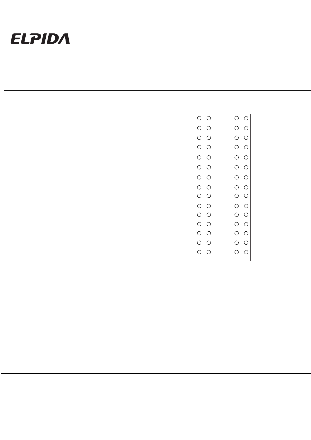
Pin Configurations
/xxx indicates active low signal.
23456
1
A
B
C
D
E
F
G
H
J
K
L
M
N
P
R
Note: ( )* marked pins are for EDS2508APSA.
A0 to A12,
BA0, BA1
DQ0 to DQ15
/CS
/RAS
/CAS
/WE
Address input
Bank select address
Data-input/output
Chip select
Row address strobe
Column address strobe
Write enable
VSS
DQ14
(NC)*
DQ13
(DQ6)*
DQ12
(NC)*
DQ10
(NC)*
DQ9
(DQ4)*
DQ8
(NC)*
NC
NC
NC
CKE
A11
A8
A6
VSSA5A4
DQ15
(DQ7)*
VSSQ
VDDQ
DQ11
(DQ5)*
VSSQ
VDDQ
NC
VSS
UDQM
(DQM)*
CLK
A12
A9
A7
(Top view)
DQM
CKE
CLK
VDD
VSS
VDDQ
VSSQ
NC
DQ0
VDD
DQ1
VDDQ
(NC)*
DQ2
VSSQ
(DQ1)*
DQ4
DQ3
(DQ2)*
(NC)*
VDDQ
DQ5
(NC)*
VSSQ
DQ6
(DQ3)*
DQ7
NC
(NC)*
VDD
NC
LDQM
/WE
(NC)*
/RAS
/CAS
NC
/CS
BA1
BA0
A0
A10
A2A3A1
VDD
Input/output mask
Clock enable
Clock input
Power for internal circuit
Ground for internal circuit
Power for DQ circuit
Ground for DQ circuit
No connection
Document No. E0228E30 (Ver. 3.0)
Date Published August 2002 (K) Japan
URL: http://www.elpida.com
Elpida Memory, Inc.2001-2002

Ordering Information
Part number
EDS2508APSA-7A
EDS2508APSA-75*
EDS2516APSA-7A
EDS2516APSA-75*
EDS2508APSA-7AL
EDS2508APSA-75L*
EDS2516APSA-7AL
EDS2516APSA-75L*
Note: 100MHz operation at /CAS latency = 2.
Mask
Version
P 32M × 8 4 133
16M × 16
32M × 8
16M × 16
Organization
(words × bits) Internal Banks
Part Number
E D S 25 04 A P SA - 7A L
Elpida Memory
Type
D: Monolithic Device
EDS2508APSA, EDS2516APSA
Clock frequency
MHz (max.)
/CAS latency Package
2, 3
3
2, 3
3
2, 3
3
2, 3
3
60-ball µBGA
Function
S: SDRAM
Density / Bank
25: 256M / 4banks
Bit Organization
08: x8
16: x16
Interface
A: 3.3V, LVTTL
Die Rev.
Package
SA: µBGA
Speed
7A: 133MHz/CL2, 3
75: 133MHz/CL3
100MHz/CL2
Power Consumption
Blank: Normal
L: Low Power
Data Sheet E0228E30 (Ver. 3.0)
2

CONTENTS
EDS2508APSA, EDS2516APSA
Description.....................................................................................................................................................1
Features.........................................................................................................................................................1
Pin Configurations .........................................................................................................................................1
Ordering Information......................................................................................................................................2
Part Number ..................................................................................................................................................2
Electrical Specifications.................................................................................................................................4
Block Diagram .............................................................................................................................................12
Pin Function.................................................................................................................................................13
Command Operation ...................................................................................................................................15
Simplified State Diagram .............................................................................................................................23
Mode Register Configuration.......................................................................................................................24
Power-up sequence.....................................................................................................................................25
Operation of the SDRAM .............................................................................................................................26
Timing Waveforms.......................................................................................................................................42
Package Drawing ........................................................................................................................................48
Recommended Soldering Conditions ..........................................................................................................49
Data Sheet E0228E30 (Ver. 3.0)
3

EDS2508APSA, EDS2516APSA
Electrical Specifications
• All voltages are referenced to VSS (GND).
• After power up (refer to the Power-up Sequence).
Absolute Maximum Ratings
Parameter Symbol Rating Unit Note
Voltage on any pin relative to VSS VT –0.5 to VDD + 0.5 (≤ 4.6 (max.)) V
Supply voltage relative to VSS VDD –0.5 to +4.6 V
Short circuit output current IOS 50 mA
Power dissipation PD 1.0 W
Operating temperature TA 0 to +70 °C
Storage temperature Tstg –55 to +125 °C
Caution
Exposing the device to stress above those listed in Absolute Maximum Ratings could cause
permanent damage. The device is not meant to be operated under conditions outside the limits
described in the operational section of this specification. Exposure to Absolute Maximum Rating
conditions for extended periods may affect device reliability.
Recommended Operating Conditions (TA = 0 to 70°°°°C)
Parameter Symbol min. max. Unit Notes
Supply voltage VDD, VDDQ 3.0 3.6 V 1
VSS, VSSQ 0 0 V 2
Input high voltage VIH 2.0 VDD + 0.3 V 3
Input low voltage VIL –0.3 0.8 V 4
Notes: 1. The supply voltage with all VDD and VDDQ pins must be on the same level.
2. The supply voltage with all VSS and VSSQ pins must be on the same level.
3. VIH (max.) = VDD + 2.0 V for pulse width ≤ 3ns at VDD.
4. VIL (min.) = VSS – 2.0 V for pulse width ≤ 3ns at VSS.
Data Sheet E0228E30 (Ver. 3.0)
4

EDS2508APSA, EDS2516APSA
DC Characteristics 1 (TA = 0 to +70°°°°C, VDD, VDDQ = 3.3V ± 0.3V, VSS, VSSQ = 0V)
Parameter max .
/CAS latency Symbol Grade × 8 × 16 Unit Test condition Notes
Operating current ICC1 -7A 130 135 mA
ICC1 -75 110 115 mA
Standby current in power
down
Standby current in power
down (input signal stable)
Standby current in non power
down
Standby current in non power
down (input signal stable)
Active standby current in
power down
Active standby current in
power down (input signal
stable)
Active standby current in non
power down
Active standby current in non
power down (input signal
stable)
Burst operating current ICC4 135 145 mA tCK = tCK (min.), BL = 4 1, 2, 5
Refresh current ICC5 -7A 250 250 mA tRC = tRC (min.) 3
ICC5 -75 220 220 mA tRC = tRC (min.)
Self refresh current ICC6 3 3 mA
Self refresh current
(L-version)
ICC2P 3 3 mA
ICC2PS 2 2 mA CKE = VIL, tCK = ∞
ICC2N 20 20 mA
ICC2NS 9 9 mA
ICC3P 4 4 mA
ICC3PS 3 3 mA CKE = VIL, tCK = ∞ 2, 7
ICC3N 30 30 mA
ICC3NS 15 15 mA
ICC6 -XXL 1 1 mA
Notes: 1. ICC depends on output load condition when the device is selected. ICC (max.) is specified at the output
open condition.
2. One bank operation.
3. Input signals are changed once per one clock.
4. Input signals are changed once per two clocks.
5. Input signals are changed once per four clocks.
6. After power down mode, CLK operating current.
7. After power down mode, no CLK operating current.
8. Input signals are VIH or VIL fixed.
Burst length = 1
tRC = tRC (min.)
Burst length = 1
tRC = tRC (min.)
CKE = VIL,
tCK = tCK (min.)
CKE, /CS = VIH,
tCK = tCK (min.)
CKE = VIH, tCK = ∞, /CS
= VIH
CKE = VIL,
tCK = tCK (min.)
CKE, /CS = VIH,
tCK = tCK (min.)
CKE = VIH, tCK = ∞, /CS
= VIH
VIH ≥ VDD – 0.2V
VIL ≤ 0.2V
1, 2, 3
6
4
8
1, 2, 6
1, 2, 4
2, 8
DC Characteristics 2 (TA = 0 to +70°°°°C, VDD, VDDQ = 3.3V ± 0.3V, VSS, VSSQ = 0V)
Parameter Symbol min. max. Unit Test condition Notes
Input leakage current ILI –1 1 µA 0 ≤ VIN ≤ VDD
Output leakage current ILO –1.5 1.5 µA 0 ≤ VOUT ≤ VDD, DQ = disable
Output high voltage VOH 2.4 — V IOH = –4 mA
Output low voltage VOL — 0.4 V IOL = 4 mA
Data Sheet E0228E30 (Ver. 3.0)
5

EDS2508APSA, EDS2516APSA
Pin Capacitance (TA = 25°C, VDD, VDDQ = 3.3V ± 0.3V)
Parameter Symbol Pins min. Typ max. Unit
Input capacitance CI1 CLK 2.0 — 3.5 pF
CI2
Data input/output capacitance CI/O DQ 4 — 6.5 pF
Address, CKE, /CS, /RAS,
/CAS, /WE, DQM,
2.0 — 3.8 pF
Notes: 1. Capacitance measured with Boonton Meter or effective capacitance measuring method.
2. Measurement condition: f = 1MHz, 1.4V bias, 200mV swing.
3. DQM = VIH to disable DOUT.
4. This parameter is sampled and not 100% tested.
AC Characteristics (TA = 0 to +70°°°°C, VDD, VDDQ = 3.3V ± 0.3V, VSS, VSSQ = 0V)
-7A -75
Parameter Symbol min. max. min. max. Unit Notes
System clock cycle time tCK 7.5 — 7.5 — ns 1
CLK high pulse width tCH 2.5 — 2.5 — ns 1
CLK low pulse width tCL 2.5 — 2.5 — ns 1
Access time from CLK tAC — 5.4 — 5.4 ns 1, 2
Data-out hold time tOH 3.0 — 3.0 — ns 1, 2
CLK to Data-out low impedance tLZ 1 — 1 — ns 1, 2, 3
CLK to Data-out high impedance tHZ — 5.4 — 5.4 ns 1, 4
Input setup time tSI 1.5 — 1.5 — ns 1
Input hold time tHI 0.8 — 0.8 — ns 1
Ref/Active to Ref/Active command
period
Active to Precharge command
period
Active command to column
command (same bank)
Precharge to active command
period
Write recovery or data-in to
precharge lead time
Last data into active latency tDAL
Active (a) to Active (b) command
period
Transition time (rise and fall) tT 0.5 5 0.5 5 ns
Refresh period
(8192 refresh cycles)
tRC 60 — 67.5 — ns 1
tRAS 45 120000 45 120000 ns 1
tRCD 15 — 20 — ns 1
tRP 15 — 20 — ns 1
tDPL 15 — 15 — ns 1
2CLK +
15ns
tRRD 15 — 15 — ns 1
tREF — 64 — 64 ms
—
2CLK +
20ns
—
Notes: 1. AC measurement assumes tT = 0.5ns. Reference level for timing of input signals is 1.4V.
2. Access time is measured at 1.4V. Load condition is CL = 50pF.
3. tLZ (min.) defines the time at which the outputs achieves the low impedance state.
4. tHZ (max.) defines the time at which the outputs achieves the high impedance state.
Notes
1, 2, 4
1, 2, 4
1, 2, 3, 4
Data Sheet E0228E30 (Ver. 3.0)
6
EDS2508APSA, EDS2516APSA
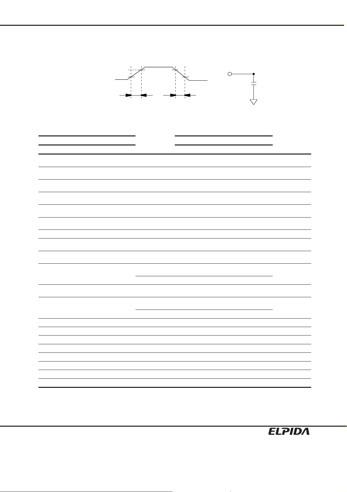
Test Conditions
• Input and output timing reference levels: 1.4V
• Input waveform and output load: See following figures
2.4 V
0.4 V
2.0 V
0.8 V
t
T
tT
input
Output load
Relationship Between Frequency and Minimum Latency
Parameter -7A -75
Frequency (MHz) 133
tCK (ns) Symbol 7.5 7.5 Notes
Active command to column command
(same bank)
Active command to active command
(same bank)
Active command to precharge command
(same bank)
Precharge command to active command
(same bank)
Write recovery or data-in to precharge
command (same bank)
Active command to active command
(different bank)
Self refresh exit time lSREX 1 1 2
Last data in to active command
(Auto precharge, same bank)
Self refresh exit to command input lSEC 8 9
Precharge command to high impedance
(CL = 2)
(CL = 3) lHZP 3 3
Last data out to active command
(Auto precharge same bank)
Last data out to precharge (early precharge)
(CL = 2)
(CL = 3) lEP –2 –2
Column command to column command lCCD 1 1
Write command to data in latency lWCD 0 0
DQM to data in lDID 0 0
DQM to data out lDOD 2 2
CKE to CLK disable lCLE 1 1
Register set to active command lMRD 2 2
/CS to command disable lCDD 0 0
Power down exit to command input lPEC 1 1
lRCD 2 3 1
lRC 8 9 1
lRAS 6 6 1
lRP 2 3 1
lDPL 2 2 1
lRRD 2 2 1
lDAL 4 5 = [lDPL + lRP]
lHZP
lAPR 1 1
lEP
2
–1
Notes: 1. IRCD to IRRD are recommended value.
2. Be valid [DESL] or [NOP] at next command of self refresh exit.
3. Except [DESL] and [NOP]
I/O
CL
= [lRC]
3
2
–1
Data Sheet E0228E30 (Ver. 3.0)
7
EDS2508APSA, EDS2516APSA
VIL/VIH Clamp
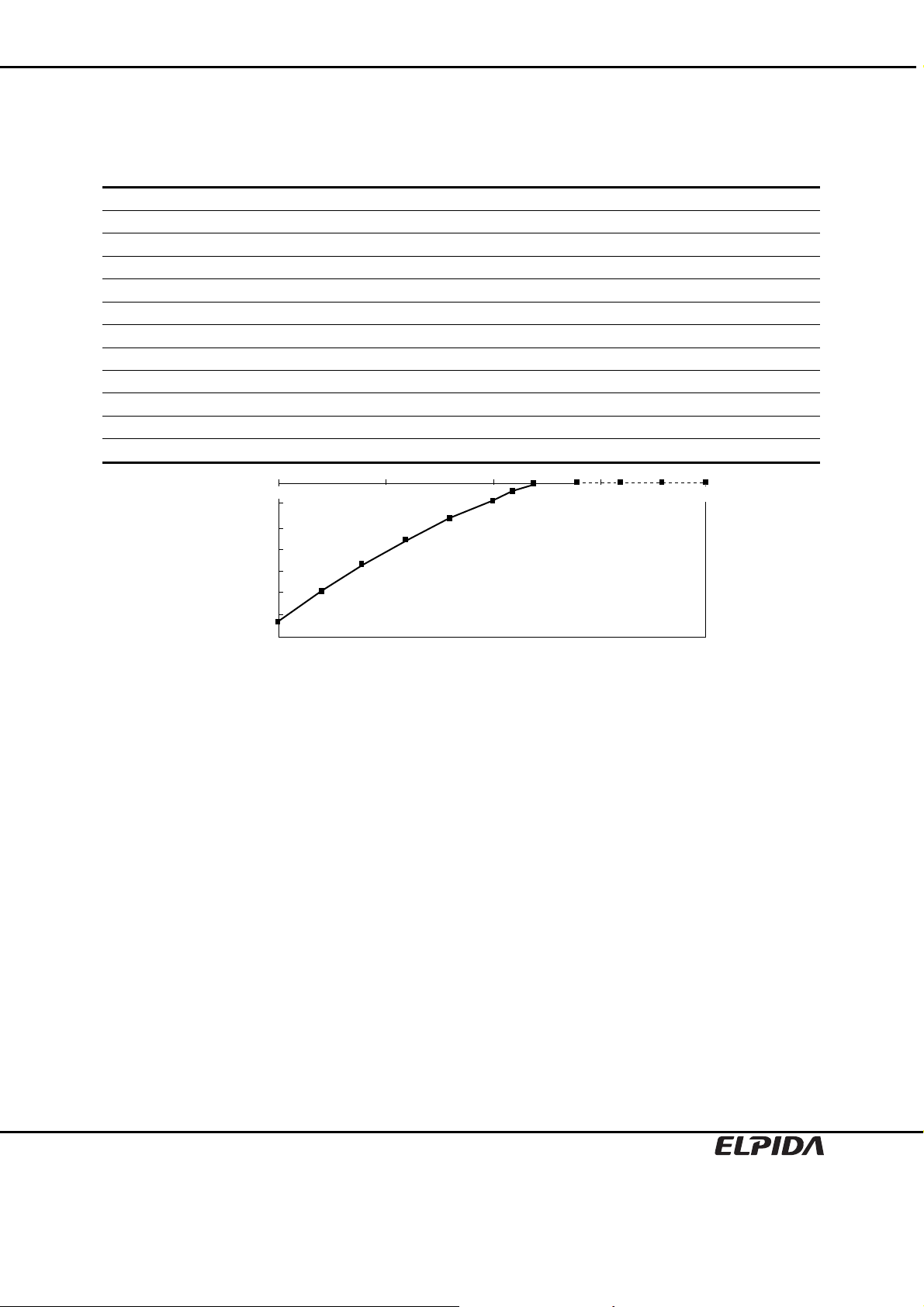
This SDRAM component has VIL and VIH clamp for CLK, CKE, /CS, DQM and DQ pins.
[Minimum VIL Clamp Current]
VIL (V) I (mA)
–2 –32
–1.8 –25
–1.6 –19
–1.4 –13
–1.2 –8
–1 –4
–0.9 –2
–0.8 –0.6
–0.6 0
–0.4 0
–0.2 0
0 0
–5
–10
–15
–20
I (mA)
–25
–30
–35
0
–2
–1.5 –1 –0.5
VIL (V)
0
Minimum VIL Clamp Current
Data Sheet E0228E30 (Ver. 3.0)
8
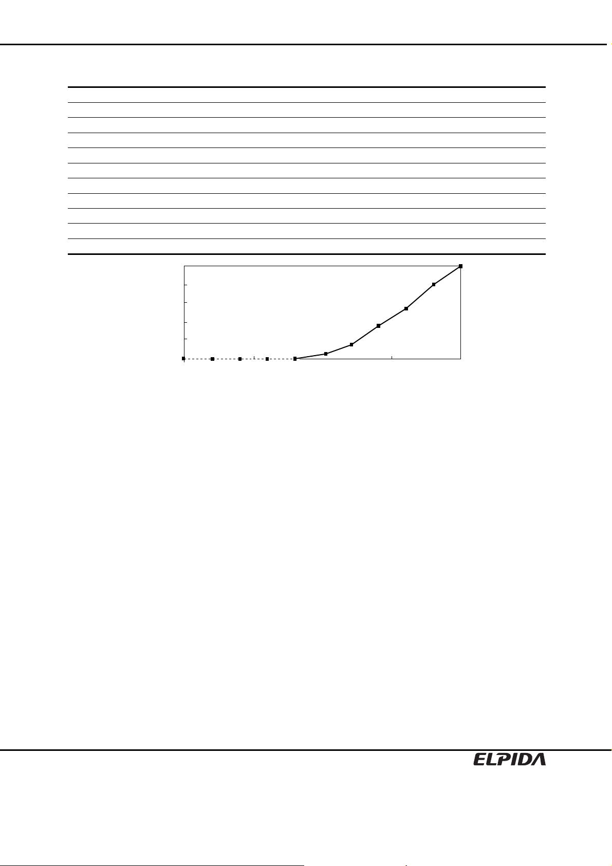
[Minimum VIH Clamp Current]
VIH (V) I (mA)
VDD + 2 10
VDD + 1.8 8
VDD + 1.6 5.5
VDD + 1.4 3.5
VDD + 1.2 1.5
VDD + 1 0.3
VDD + 0.8 0
VDD + 0.6 0
VDD + 0.4 0
VDD + 0.2 0
VDD + 0 0
10
8
6
I (mA)
4
2
EDS2508APSA, EDS2516APSA
0
VDD + 0 VDD + 1 VDD + 2VDD + 0.5 VDD + 1.5
VIH (V)
Minimum VIH Clamp Current
Data Sheet E0228E30 (Ver. 3.0)
9
EDS2508APSA, EDS2516APSA
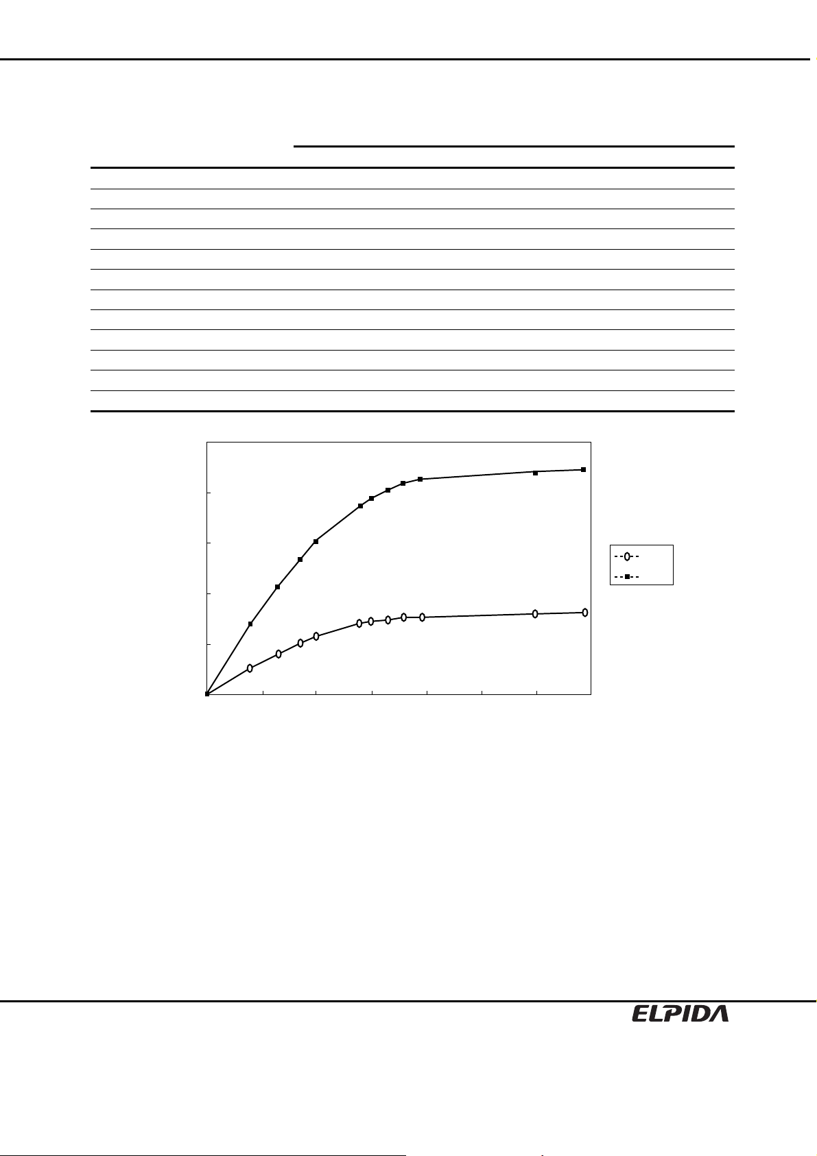
IOL/IOH Characteristics
[Output Low Current (IOL)]
IOL IOL
VOUT (V) min. (mA) max. (mA)
0 0 0
0.4 27 71
0.65 41 108
0.85 51 134
1 58 151
1.4 70 188
1.5 72 194
1.65 75 203
1.8 77 209
1.95 77 212
3 80 220
3.45 81 223
250
200
150
IOL (mA)
100
50
0
0 0.5 1 1.5 2 2.5 3 3.5
VOUT (V)
Output Low Current (IOL)
min.
max.
Data Sheet E0228E30 (Ver. 3.0)
10
EDS2508APSA, EDS2516APSA
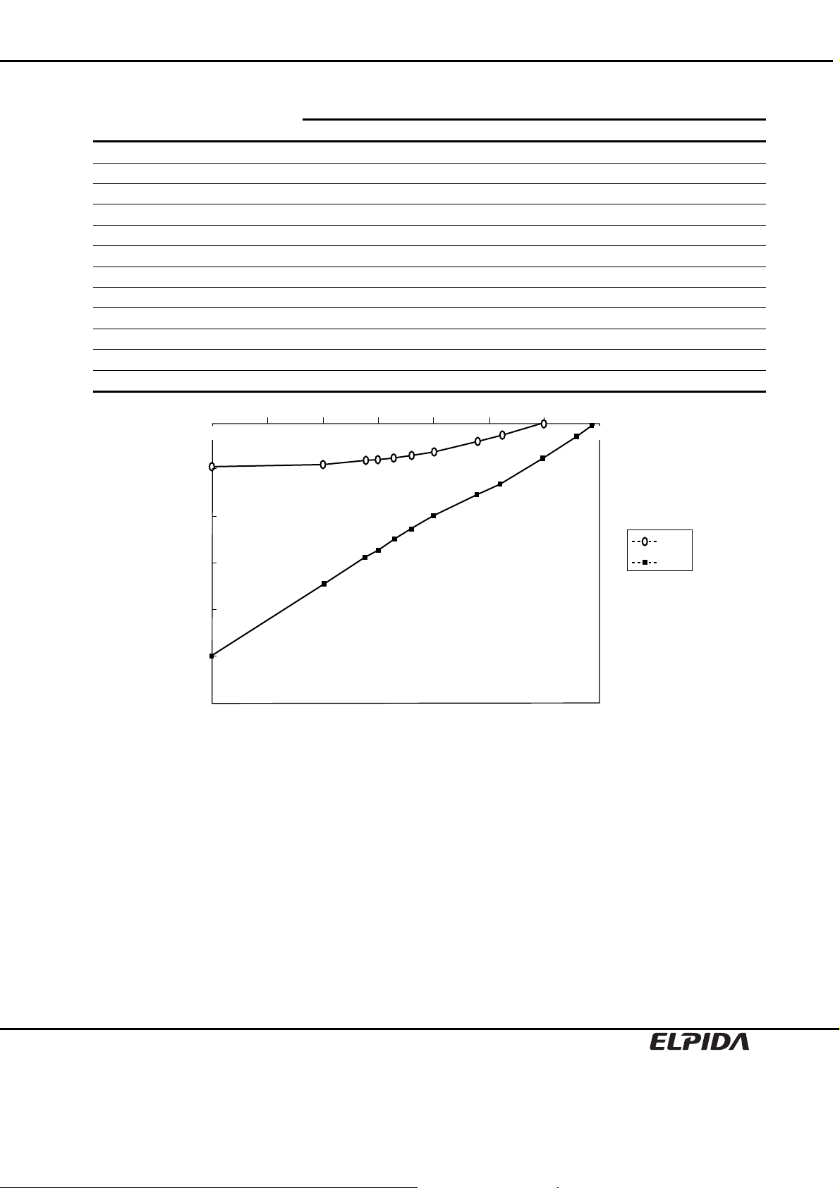
[Output High Current (IOH)]
IOH IOH
VOUT (V) min. (mA) max. (mA)
3.45 — –3
3.3 — –28
3 0 –75
2.6 –21 –130
2.4 –34 –154
2 –59 –197
1.8 –67 –227
1.65 –73 –248
1.5 –78 –270
1.4 –81 –285
1 –89 –345
0 –93 –503
0
0.5 1 1.5 2 2.5 3
3.50
–100
–200
IOH (mA)
–300
–400
–500
–600
VOUT(V)
Output High Current (IOH)
min.
max.
Data Sheet E0228E30 (Ver. 3.0)
11
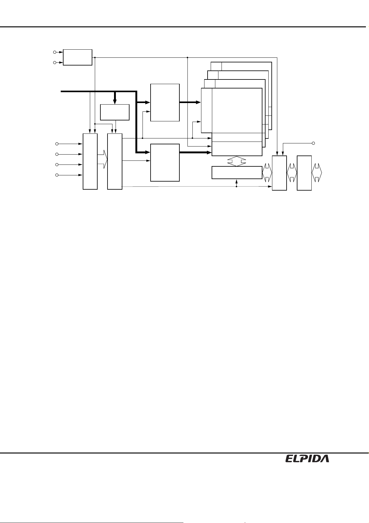
Block Diagram
CLK
CKE
Address
/CS
/RAS
/CAS
/WE
Clock
Generator
Mode
Register
Control Logic
Command Decoder
Row
Address
Buffer
&
Refresh
Counter
Column
Address
Buffer
&
Burst
Counter
EDS2508APSA, EDS2516APSA
Bank 3
Bank 2
Bank 1
Bank 0
Row Decoder
Sense Amplifier
Column Decoder &
Latch Circuit
Data Control Circuit
Latch Circuit
DQM
DQ
Input & Output
Buffer
Data Sheet E0228E30 (Ver. 3.0)
12

EDS2508APSA, EDS2516APSA
Pin Function
CLK (input pin)
CLK is the master clock input to this pin. The other input signals are referred at CLK rising edge.
/CS (input pin)
When /CS is Low, the command input cycle becomes valid. When /CS is High, all inputs are ignored. However,
internal operations (bank active, burst operations, etc.) are held.
/RAS, /CAS, and /WE (input pins)
Although these pin names are the same as those of conventional DRAMs, they function in a different way. These
pins define operation commands (read, write, etc.) depending on the combination of their voltage levels. For details,
refer to the command operation section.
A0 toA12 (input pins)
Row address (AX0 to AX12) is determined by A0 to A12 at the bank active command cycle CLK rising edge.
Column address is determined by A0 to A8, A9 or A11 (see Address Pins Table) at the read or write command cycle
CLK rising edge. And this column address becomes burst access start address.
[Address Pins Table]
Address (A0 to A12)
Part number Row address Column address
EDS2504AP AX0 to AX12 AY0 to AY9, AY11
EDS2508AP AX0 to AX12 AY0 to AY9
EDS2516AP AX0 to AX12 AY0 to AY8
A10 defines the precharge mode. When A10 = High at the precharge command cycle, all banks are precharged.
But when A10 = Low at the precharge command cycle, only the bank that is selected by BA0 and BA1 (BS) is
precharged. For details refer to the command operation section.
BA0 and BA1 (input pin)
BA0 and BA1 are bank select signal (BS). (See Bank Select Signal Table)
[Bank Select Signal Table]
BA0 BA1
Bank 0 L L
Bank 1 H L
Bank 2 L H
Bank 3 H H
Remark: H: VIH. L: VIL.
CKE (input pin)
This pin determines whether or not the next CLK is valid. If CKE is High, the next CLK rising edge is valid. If CKE is
Low, the next CLK rising edge is invalid. This pin is used for power-down mode, clock suspend mode and self
refresh mode.
Data Sheet E0228E30 (Ver. 3.0)
13

EDS2508APSA, EDS2516APSA
DQM, UDQM and LDQM (input pins)
DQM controls input/output buffers. In 16M × 16 products, UDQM and LDQM control upper byte (DQ8 to DQ15) and
lower byte (DQ0 to DQ7).
Read operation: If DQM is High, the output buffer becomes High-Z. If the DQM is Low, the output buffer becomes
Low-Z. (The latency of DQM during reading is 2 clocks.)
Write operation: If DQM is High, the previous data is held (the new data is not written). If DQM is Low, the data is
written. (The latency of DQM during writing is 0 clock.)
DQ0 toDQ15 (input/output pins)
Data is input to and output from these pins (DQ0 to DQ3; EDS2504AP , DQ0 to DQ7; EDS2508AP, DQ0 to DQ15;
EDS2516AP).
VDD, VSS, VDDQ, VSSQ (Power supply)
VDD and VSS are power supply pins for internal circuits. VDDQ and VSSQ are power supply pins for the output
buffers.
Data Sheet E0228E30 (Ver. 3.0)
14

EDS2508APSA, EDS2516APSA
Command Operation
Command Truth Table
The SDRAM recognizes the following commands specified by the /CS, /RAS, /CAS, /WE and address pins.
CKE
Function Symbol n – 1 n /CS /RAS /CAS /WE BA1,BA0 A10
Device deselect DESL H × H × × × × × ×
No operation NOP H × L H H H × × ×
Burst stop BST H × L H H L × × ×
Read READ H × L H L H V L V
Read with auto precharge READA H × L H L H V H V
Write WRIT H × L H L L V L V
Write with auto precharge WRITA H × L H L L V H V
Bank activate ACT H × L L H H V V V
Precharge select bank PRE H × L L H L V L ×
Precharge all banks PALL H × L L H L × H ×
Mode register set MRS H × L L L L L L V
Remark: H: VIH. L: VIL. ×: VIH or VIL. V: Valid address input.
Device deselect command [DESL]
When this command is set (/CS is High), the SDRAM ignore command input at the clock. However, the internal
status is held.
No operation [NOP]
This command is not an execution command. However, the internal operations continue.
Burst stop command [BST]
This command can stop the current burst operation.
Column address strobe and read command [READ]
This command starts a read operation. In addition, the start address of burst read is determined by the column
address (see Address Pins Table in Pin Function) and the bank select address (BA0, BA1). . After the read
operation, the output buffer becomes High-Z.
Read with auto-precharge [READA]
This command automatically performs a precharge operation after a burst read with a burst length of 1, 2, 4 or 8.
Column address strobe and write command [WRIT]
This command starts a write operation. When the burst write mode is selected, the column address (see Address
Pins Table in Pin Function) and the bank select address (BA0, BA1) become the burst write start address. When the
single write mode is selected, data is only written to the location specified by the column address (see Address Pins
Table in Pin Function) and the bank select address (BA0, BA1).
Write with auto-precharge [WRITA]
This command automatically performs a precharge operation after a burst write with a length of 1, 2, 4 or 8, or after a
single write operation.
A0 to A12
Data Sheet E0228E30 (Ver. 3.0)
15

EDS2508APSA, EDS2516APSA
Row address strobe and bank activate [ACT]
This command activates the bank that is selected by BA0, BA1 and determines the row address (AX0 to AX12).
(See Bank Select Signal Table)
Precharge selected bank [PRE]
This command starts precharge operation for the bank selected by BA0, BA1. (See Bank Select Signal Table)
[Bank Select Signal Table]
BA0 BA1
Bank 0 L L
Bank 1 H L
Bank 2 L H
Bank 3 H H
Remark: H: VIH. L: VIL.
Precharge all banks [PALL]
This command starts a precharge operation for all banks.
Refresh [REF/SELF]
This command starts the refresh operation. There are two types of refresh operation, the one is auto-refresh, and
the other is self-refresh. For details, refer to the CKE truth table section.
Mode register set [MRS]
The SDRAM has a mode register that defines how it operates. The mode register is specified by the address pins
(A0 to BA0 and BA1) at the mode register set cycle. For details, refer to the mode register configuration. After
power on, the contents of the mode register are undefined, execute the mode register set command to set up the
mode register.
Data Sheet E0228E30 (Ver. 3.0)
16
 Loading...