ELPID EDS1232CATA-75L, EDS1232CATA-75, EDS1232CATA-1AL, EDS1232CATA-1A, EDS1232CABB-75L-E Datasheet
...
PRELIMINARY DATA SHEET
128M bits SDRAM
EDS1232CABB, EDS1232CATA (4M words ×××× 32 bits)
Description
The EDS1232CA is a 128M bits SDRAM organized as
1,048,576 words × 32 bits × 4 banks. All inputs and
outputs are synchronized with the positive edge of the
clock.
They are packaged in 90-ball FBGA, 86-pin plastic
TSOP (II).
Features
• 2.5V power supply
• Clock frequency: 133MHz (max.)
• Single pulsed /RAS
• ×32 organization
• 4 banks can operate simultaneously and
independently
• Burst read/write operation and burst read/single write
operation capability
• Programmable burst length (BL): 1, 2, 4, 8 and full
page
• 2 variations of burst sequence
Sequential (BL = 1, 2, 4, 8)
Interleave (BL = 1, 2, 4, 8)
• Programmable /CAS latency (CL): 2, 3
• Byte control by DQM
• Refresh cycles: 4096 refresh cycles/64ms
• 2 variations of refresh
Auto refresh
Self refresh
• FBGA package is lead free solder (Sn-Ag-Cu)
Document No. E0247E40 (Ver. 4.0)
Date Published July 2002 (K) Japan
URL: http://www.elpida.com
Elpida Memory, Inc. 2002

EDS1232CABB, EDS1232CATA
Ordering Information
Part number
EDS1232CABB-75-E 2.5V 4M × 32 4 133 3 90-ball FBGA
EDS1232CABB-1A-E 100 2, 3
EDS1232CABB-75L-E 133 3
EDS1232CABB-1AL-E 100 2, 3
EDS1232CATA-75 2.5V 4M × 32 4 133 3 86-pin plastic
EDS1232CATA-1A 100 2, 3 TSOP (II)
EDS1232CATA-75L 133 3
EDS1232CATA-1AL 100 2, 3
Supply
voltage
Organization
(words × bits) Internal Banks
Clock frequency
MHz (max.)
/CAS latency Package
Part Number
E D S 12 32 C A BB - 75 L - E
Elpida Memory
Type
D: Monolithic Device
Product Code
S: SDRAM
Density / Bank
12: 128M/4 Banks
Bit Organization
32: x32
Voltage, Interface
C: 2.5V, LVTTL
Die Revision
Lead Free
Power Consumption
Blank: Normal
L: Low Power
Speed
75: 133MHz/CL3
100MHz/CL2
1A: 100MHz/CL2,3
Package
TA: TSOP (II)
BB: FBGA
Preliminary Data Sheet E0247E40 (Ver. 4.0)
2
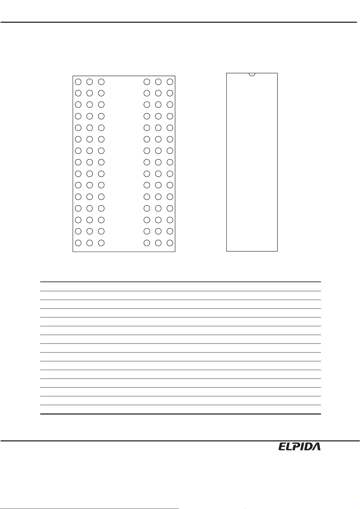
Pin Configurations
/xxx indic ate active low signal.
EDS1232CABB, EDS1232CATA
90-ball FBGA
1
23456789
A
DQ26
B
DQ28
C
VSSQ
D
VSSQ
E
VDDQ
F
VSS
G
A4
H
A7
J
CLK
K
DQM1 NC NC /CAS /WE DQM0
L
VDDQ DQ8 VSS VDD DQ7 VSSQ
M
VSSQ DQ10 DQ9 DQ6 DQ5 VDDQ
N
VSSQ DQ12 DQ14 DQ1 DQ3 VDDQ
P
DQ11 VDDQ VSSQ VDDQ VSSQ DQ4
R
DQ13 DQ15 VSS VDD DQ0 DQ2
DQ24
VDDQ
DQ27
DQ29
DQ31
DQM3
A5
A8
CKE
VSS
VSSQ
DQ25
DQ30
NC
A3
A6
NC
A9
VDD
VDDQ
DQ22
DQ17
NC
A2
A10
NC
BA0
DQ23
VSSQ
DQ20
DQ18
DQ16
DQM2
BA1
/CS
VDD
DQ0
DQ21
DQ19
VDDQ
VDDQ
VSSQ
VDD
A0
A1
A11
/RAS
VDDQ
DQ1
DQ2
VSSQ
DQ3
DQ4
VDDQ
DQ5
DQ6
VSSQ
DQ7
NC
VDD
DQM0
/WE
/CAS
/RAS
/CS
A11
BA0
BA1
A10(AP)
A0
A1
A2
DQM2
VDD
NC
DQ16
VSSQ
DQ17
DQ18
VDDQ
DQ19
DQ20
VSSQ
DQ21
DQ22
VDDQ
DQ23
VDD
1
2
3
4
5
6
7
8
9
10
11
12
13
14
15
16
17
18
19
20
21
22
23
24
25
26
27
28
29
30
31
32
33
34
35
36
37
38
39
40
41
42
43
86-pin TSOP
86
85
84
83
82
81
80
79
78
77
76
75
74
73
72
71
70
69
68
67
66
65
64
63
62
61
60
59
58
57
56
55
54
53
52
51
50
49
48
47
46
45
44
V
SS
DQ15
VSSQ
DQ14
DQ13
VDDQ
DQ12
DQ11
VSSQ
DQ10
DQ9
VDDQ
DQ8
NC
VSS
DQM1
NC
NC
CLK
CKE
A9
A8
A7
A6
A5
A4
A3
DQM3
VSS
NC
DQ31
VDDQ
DQ30
DQ29
VSSQ
DQ28
DQ27
VDDQ
DQ26
DQ25
VSSQ
DQ24
VSS
(Top view) (Top view)
Pin name Function
A0 to A11 Address inputs
BA0, BA1 Bank select
DQ0 to DQ31 Data input/output
CLK Clock input
CKE Clock enable
/CS Chip select
/RAS Row address strobe
/CAS Column address strobe
/WE Write enable
DQM0 to DQM3 DQ mask enable
VDD Supply voltage
VSS Ground
VDDQ Supply voltage for DQ
VSSQ Ground for DQ
NC No connection
Preliminary Data Sheet E0247E40 (Ver. 4.0)
3

CONTENTS
EDS1232CABB, EDS1232CATA
Description.................................................................................................................................................... 1
Features........................................................................................................................................................ 1
Ordering Information.....................................................................................................................................2
Part Number.................................................................................................................................................. 2
Pin Configurations......................................................................................................................................... 3
Electrical Specific atio ns ................................................................................................................................5
Block Diagram............................................................................................................................................. 10
Pin Function................................................................................................................................................ 11
Command Operation................................................................................................................................... 12
Truth Table.................................................................................................................................................. 16
Simplified State Diagram ............................................................................................................................ 22
Programming Mode Registers.................................................................................................................... 23
Mode Register.............................................................................................................................................24
Power-up sequence.................................................................................................................................... 27
Operation of the SDRAM ............................................................................................................................ 28
Timing Waveforms......................................................................................................................................44
Package Drawing........................................................................................................................................ 51
Recommended Soldering Conditions .........................................................................................................53
Revision History..........................................................................................................................................56
Preliminary Data Sheet E0247E40 (Ver. 4.0)
4

EDS1232CABB, EDS1232CATA
Electrical Specifications
• All voltages are referenced to VSS (GND).
• After power up (refer to the Power up sequence).
Absolute Maximum Ratings
Parameter Symbol Rating Unit Note
Voltage on any pin relative to VSS VT
Supply voltage relative to VSS VDD, VDDQ
Short circuit output current IOS 50 mA
Power dissipation PD 1.0 W
Operating ambient temperature TA 0 to +70 °C
Storage temperature Tstg –55 to +125 °C
Caution
Exposing the device to stress above those listed in Absolute Maximum Ratings could cause
permanent damage. The device is not meant to be operated under conditions outside the limits
described in the operational section of this specification. Exposure to Absolute Maximum Rating
conditions for extended periods may affect device reliability.
Recommended Operating Conditions (TA = 0 to +70°°°°C)
–0.5 to +3.6
–0.5 to +3.6
V
V
Parameter Symbol min. typ. max. Unit Notes
Supply voltage VDD, VDDQ 2.3 2.5 2.7 V
Input high voltage VIH 1.7 VDD + 0.3*1 V
Input low voltage VIL –0.3 0.7 V
VSS 0 0 0 V
Notes: 1. VIH (max.) = VDDQ + 1.5V (pulse width ≤ 5ns).
2. VIL (min.) = –1.5V (pulse width ≤ 5ns).
Preliminary Data Sheet E0247E40 (Ver. 4.0)
5

EDS1232CABB, EDS1232CATA
DC Characteristics (TA = 0 to +70°°°°C, VDD, VDDQ = 2.5V±±±±0.2V, VSS, VSSQ = 0V)
Parameter
/CAS latency Symbol Grade max. Unit Tes t c ondition Notes
Operating current
(CL = 2)
(CL = 3) IDD1
Standby current in power down IDD2P 1 mA
Standby current in power down
(input signal stable)
Standby current in non power
down
Standby current in non power
down
(input signal stable)
Active standby current in power
down
Active standby current in power
down (input signal stable)
Active standby current in non
power down
Active standby current in non
power down
(input signal stable)
Burst operating current IDD4
Refresh current IDD5
Self refresh current IDD6 2.0 mA
Self refresh current
(L-version)
IDD1
IDD2PS 1 mA
IDD2N 20 mA
IDD2NS 8 mA CKE ≥ VIH (min.) tCK = ∞
IDD3P 5 mA CKE ≤ VIL (max.) tCK = 15ns
IDD3PS 4 mA CKE ≤ VIL (max.), tCK = ∞
IDD3N 25 mA
IDD3NS 15 mA CKE ≥ VIH (min.), tCK = ∞,
IDD6 -xxL 0.6 mA
-75
-1A
-75
-1A
-75
-1A
-75
-1A
Notes: 1. IDD1 depends on output loading and cycle rates. Specified values are obtained with the output open. In
addition to this, IDD1 is measured condition that addresses are changed only one time during tCK (min.).
2. IDD4 depends on output loading and cycle rates. Specified values are obtained with the output open.
In addition to this, IDD4 is measured condition that addresses are changed only one time during tCK
(min.).
3. IDD5 is measured on condition that addresses are changed only one time during tCK (min.).
105
100
105
100
150
130
210
200
mA 1
mA
mA
mA tRC ≥ tRC (min.) 3
Burst length = 1
tRC ≥ tRC (min.)
IO = 0mA
One bank active
CKE ≤ VIL (max.) tCK = 15ns
CKE ≤ VIL (max.) tCK = ∞
CKE ≥ VIH (min.) tCK = 15ns
CS ≥ VIH (min.)
Input signals are changed one
time during 30ns
CKE ≥ VIH (min.), tCK = 15 ns,
/CS ≥ VIH (min.),
Input signals are changed one
time during 30ns.
tCK ≥ tCK (min.),
IO = 0mA, All banks active
VIH ≥ VDD − 0.2V,
VIL ≤ GND + 0.2V
2
DC Characteristics 2 (TA = 0 to +70°°°°C, VDD, VDDQ = 2.5V±±±±0.2V, VSS, VSSQ = 0V)
Parameter Symbol min. max. Unit Test condition Notes
Input leakage current ILI –1.0 1.0 µA
Output leakage current ILO –1.5 1.5 µA 0 = VIN = VDDQ DOUT is disabled
Output high voltage
Output low voltage
VOH 2.0 — V IOH = –1mA
VOL — 0.4 V IOL = 1mA
0 = VIN = VDDQ, VDDQ = VDD,
All other pins not under test = 0V
Preliminary Data Sheet E0247E40 (Ver. 4.0)
6

EDS1232CABB, EDS1232CATA
Pin Capacitance (TA = 25°C, f = 1MHz)
90-ball FBGA 86-pin TSOP (II)
Parameter Symbol Pins min. Typ max. min. Typ max. Unit
Input capacitance CI1 Address 1.5 — 3.0 2.5 — 4.0 pF
CI2
Data input/output
capacitance
CI/O DQ 3.0 — 5.5 4.0 — 6.5 pF
CLK, CKE, /CS, /RAS,
/CAS, /WE, DQM
1.5 — 3.0 2.5 — 4.0 pF
AC Characteristics (TA = 0 to +70°°°°C, VDD, VDDQ = 2.5V±±±±0.2V, VSS, VSSQ = 0V)
-75 -1A
Parameter Symbol min. max. min. max. Unit Notes
System clock cy cl e time
(CL = 2)
(CL = 3) tCK 7.5 — 10 — ns
CLK high pulse width tCH 2.5 — 3 — ns
CLK low pulse width tCL 2.5 — 3 — ns
Access time from CLK tAC — 5.4 — 6 ns
Data-out hold time tOH 2 — 2 — ns
CLK to Data-out low impedance tLZ 0 — 0 — ns
CLK to Data-out high impedance tHZ 2 5.4 2 6 ns
Input setup time tSI 1.5 — 2 — ns
Input hold time tHI 0.8 — 1 — ns
CKE setup time (Power down exit) tCKSP 1.5 — 2 — ns
ACT to REF/ACT command period
(operation)
(refresh) tRC 67.5 70 ns
Active to Precharge command period tRAS 45 120000 50 120000 ns
Active command to column command
(same bank)
Precharge to active command period tRP 20 20 ns
Write recovery or data-in to precharge
lead time
Last data into active latency tDAL
Active (a) to Active (b) command period tRRD 15 20 — ns
Mode register set cycle time tRSC 2 2 CLK
Transition time (rise and fall) tT 0.5 30 0.5 30 ns
Refresh period
(4096 refresh cycles)
tCK 10 — 10 — ns
tRC 67.5 70 ns
tRCD 20 20 ns
tDPL 15 20 ns
2CLK +
20ns
tREF — 64 — 64 ms
2CLK +
20ns
—
Notes
Preliminary Data Sheet E0247E40 (Ver. 4.0)
7
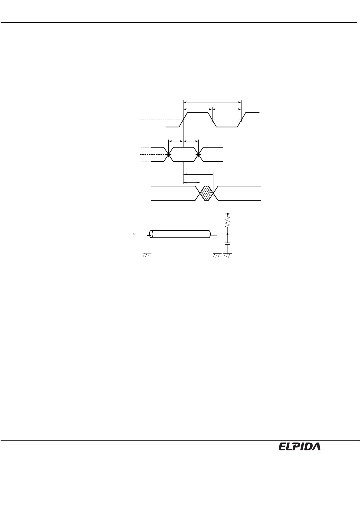
Test Conditions
• AC high level input voltage / low level input voltage: 2.1V / 0.3V
• Input timing measurement reference level: 1.2V
• Transition time (Input rise and fall time): 1ns
• Output timing measurement reference level: 1.2V
• Termination voltage (Vtt): 1.2V
tCH tCL
2.1V
CLK
Input
Output
1.2V
0.3V
tSETUP tHOLD
2.1V
1.2V
0.3V
tAC
tOH
EDS1232CABB, EDS1232CATA
tCK
Vtt
50
Z = 50 Ω
Output
Ω
30pF
Input Waveforms and Output Load
Preliminary Data Sheet E0247E40 (Ver. 4.0)
8

EDS1232CABB, EDS1232CATA
Relationship Between Frequency and Minimum Latency
Parameter -75 -1A
Frequency (MHz) 133 100 100 77
tCK (ns) Symbol 7.5 10 10 13 Notes
Active command to column command
(same bank)
Active command to active command
(same bank)
Active command to precharge command
(same bank)
Precharge command to active command
(same bank)
Write recovery or data-in to precharge
command (same bank)
Active command to active command
(different bank)
Self refresh exit time lSREX 1 1 1 1 2
Last data in to active command
(Auto precharge, same bank)
Self refresh exit to command input lSEC 9 7 7 6
Precharge command to high impedance
(CL = 2)
(CL = 3) lHZP 3 3 3 3
Last data out to active command
(auto precharge) (same bank)
Last data out to precharge
(early precharge)
(CL = 2)
(CL = 3) lEP –2 –2 –2 –2
Column command to column command lCCD 1 1 1 1
Write command to data in latency lWCD 0 0 0 0
DQM to data in lDID 0 0 0 0
DQM to data out lDOD 2 2 2 2
CKE to CLK disable lCLE 1 1 1 1
Register set to active command lMRD 2 2 2 2
/CS to command disable lCDD 0 0 0 0
Power down exit to command input lPEC 1 1 1 1
Notes: 1. IRCD to IRRD are recommended value.
2. Be valid [DESL] or [NOP] at next command of self refresh exit.
3. Except [DESL] and [NOP]
lRCD 3 2 2 2 1
lRC 9 7 7 6 1
lRAS 6 5 5 4 1
lRP 3 2 2 2 1
lDPL 2 2 2 2 1
lRRD 2 2 2 2 1
lDAL 5 4 4 4 = [lDPL + lRP]
= [lRC]
3
lHZP 2 2 2
lAPR 1 1 1 1
lEP –1 –1 –1
Preliminary Data Sheet E0247E40 (Ver. 4.0)
9
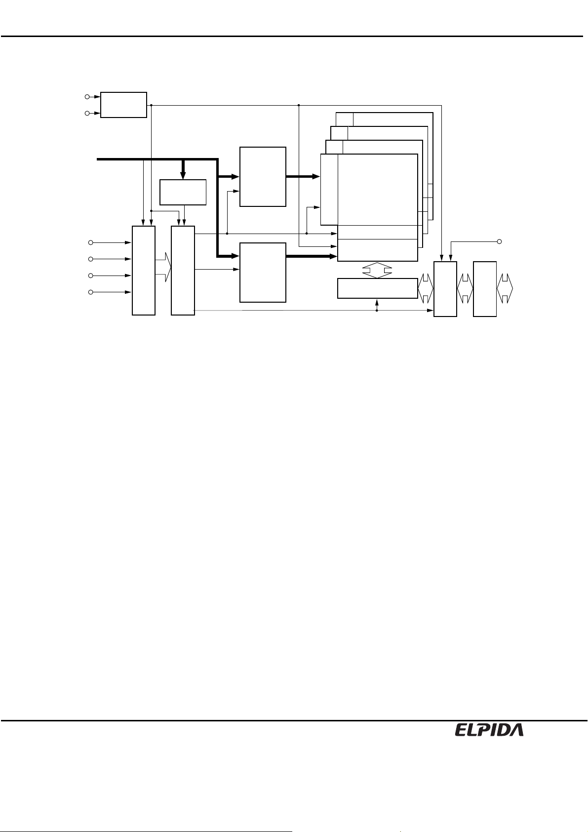
Block Diagram
CLK
CKE
Address
/CS
/RAS
/CAS
/WE
Clock
Generator
Mode
Register
Control Logic
Command Decoder
Row
Address
Buffer
&
Refresh
Counter
Column
Address
Buffer
&
Burst
Counter
EDS1232CABB, EDS1232CATA
Bank 3
Bank 2
Bank 1
Bank 0
Row Decoder
Sense Amplifier
Column Decoder &
Latch Circuit
Data Control Circuit
Latch Circuit
DQM
DQ
Input & Output
Buffer
Preliminary Data Sheet E0247E40 (Ver. 4.0)
10

EDS1232CABB, EDS1232CATA
Pin Function
CLK (input pin)
CLK is the master clock input. Other inputs signals are referenced to the CLK rising edge.
CKE (input pins)
CKE determine validity of the next CLK (clock). If CKE is high, the next CLK rising edge is valid; otherwise it is
invalid. If the CLK rising edge is invalid, the internal clock is not issued and the Synchronous DRAM suspends
operation.
When the Synchronous DRAM is not in burst mode and CKE is negated, the device enters power down mode.
During power down mode, CKE must remain low.
/CS (input pins)
/CS low starts the command input cycle. When /CS is high, commands are ignored but operations continue.
/RAS, /CAS, and /WE (input pins)
/RAS, /CAS and /WE have the same symbols on conventional DRAM but different functions. For details, refer to the
command table.
A0 to A11 (input pins)
Row Address is determined by A0 to A11 at the CLK (clock) rising edge in the active command cycle.
Column Address is determined by A0 to 7 at the CLK rising edge in the read or write command cycle.
A10 defines the precharge mode. When A10 is high in the precharge command cycle, all banks are precharged;
when A10 is low, only the bank selected by BA0 and BA1 is precharged.
When A10 is high in read or write command cycle, the precharge starts automatically after the burst access.
BA0 and BA1 (input pin)
BA0 and BA1 are bank select signal. (See Bank Select Signal Table)
[Bank Select Signal Table]
BA0 BA1
Bank 0 L L
Bank 1 H L
Bank 2 L H
Bank 3 H H
Remark: H: VIH. L: VIL.
DQM (input pins)
DQM controls I/O buffers. DQM0 controls DQ0 to 7, DQM1 controls DQ8 to DQ15, DQM2 controls DQ16 to DQ23,
DQM3 controls DQ24 to DQ31. In read mode, DQM controls the output buffers like a conventional /OE pin. DQM
high and DQM low turn the output buffers off and on, respectively. The DQM latency for the read is two clocks. In
write mode, DQM controls the word mask. Input data is written to the memory cell if DQM is low but not if DQM is
high. The DQM latency for the write is zero.
DQ0 to DQ31 (input/output pins)
DQ pins have the same function as I/O pins on a conventional DRAM.
VDD, VSS, VDDQ, VSSQ (Power supply)
VDD and VSS are power supply pins for internal circuits. VDDQ and VSSQ are power supply pins for the output
buffers.
Preliminary Data Sheet E0247E40 (Ver. 4.0)
11
EDS1232CABB, EDS1232CATA
Command Operation
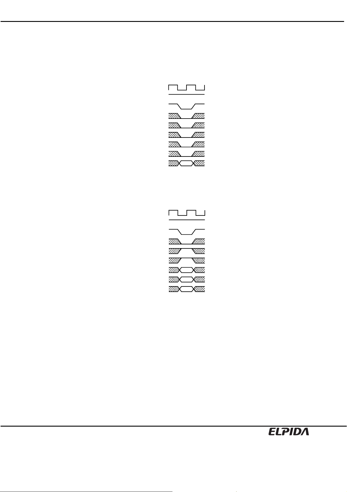
Mode register set command (/CS, /RAS, /CAS, /WE)
The Synchronous DRAM has a mode register that defines how the device operates. In this command, A0 through
A11 are the data input pins. After power on, the mode register set command must be executed to initialize the
device. The mode register can be set only when all banks are in idle state. During 2CLK (tRSC) following this
command, the Synchronous DRAM cannot accept any other commands.
CLK
CKE
H
/CS
/RAS
/CAS
/WE
BA0, BA1
(Bank select)
A10
Add
Mode Register Set Command
Activate command (/CS, /RAS = Low, /CAS, /WE = High)
The Synchronous DRAM has four banks, each with 4,096 rows. This command activates the bank selected by BA0
and BA1 and a row address selected by A0 through A11. This command corresponds to a conventional DRAM's
/RAS falling.
CLK
CKE
H
/CS
/RAS
/CAS
/WE
BA0, BA1
(Bank select)
A10
Add
Row
Row
Row Address Strobe and Bank Activate Command
Preliminary Data Sheet E0247E40 (Ver. 4.0)
12
EDS1232CABB, EDS1232CATA
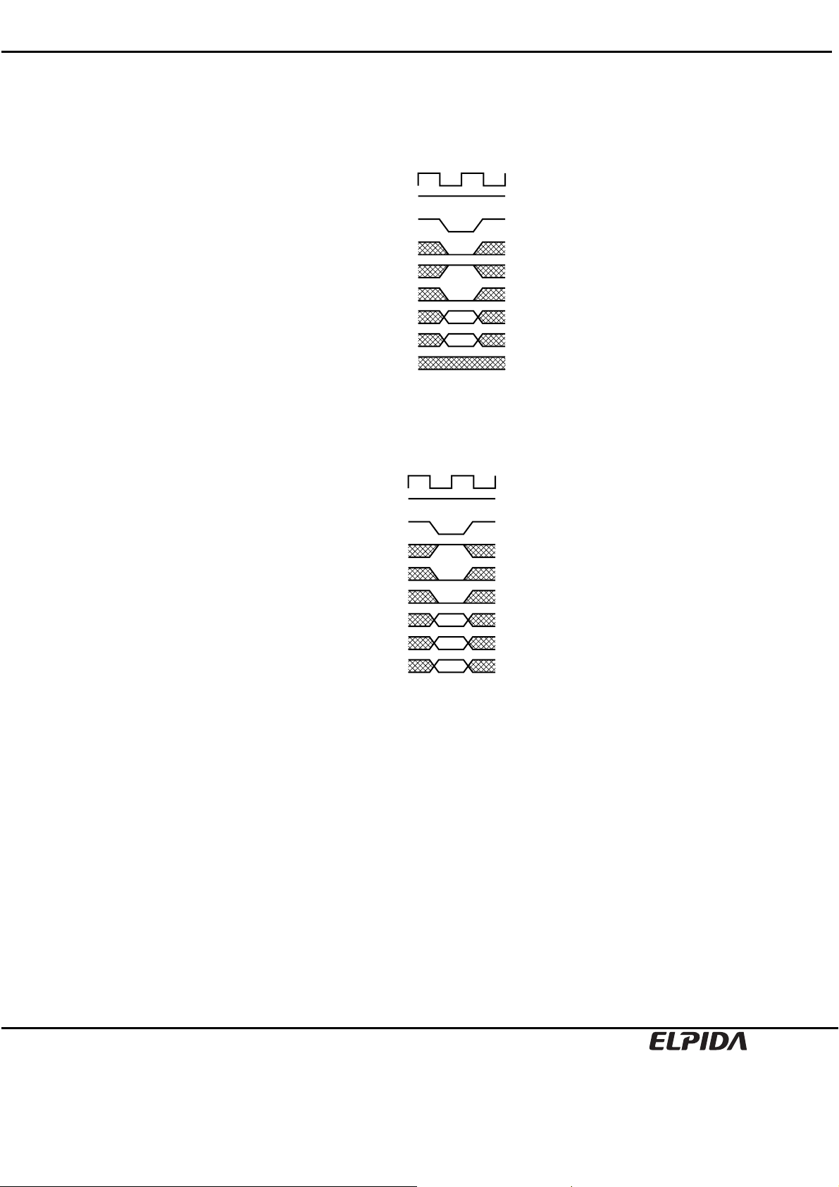
Precharge command (/CS, /RAS, /WE = Low, /CAS = High)
This command begins precharge operation of the bank selected by BA0 and BA1. When A10 is High, all banks are
precharged, regardless of BA0 and BA1. When A10 is Low, only the bank selected by BA0 and BA1 is precharged.
After this command, the Synchronous DRAM can’t accept the activate command to the precharging bank during tRP
(precharge to activate command period). This command corresponds to a conventional DRAM’s /RAS rising.
CLK
CKE
H
/CS
/RAS
/CAS
/WE
BA0, BA1
(Bank select)
(Precharge select)
Write command (/CS, /CAS, /WE = Low, /RAS = High)
If the mode register is in the burst write mode, this command sets the burst start address given by the column
address to begin the burst write operation. The first write data in burst mode can input with this command with
subsequent data on following clocks.
A10
Add
Precharge Command
CLK
CKE
H
/CS
/RAS
/CAS
/WE
BA0, BA1
(Bank select)
A10
Add
Col.
Column Address and Write Command
Preliminary Data Sheet E0247E40 (Ver. 4.0)
13
EDS1232CABB, EDS1232CATA
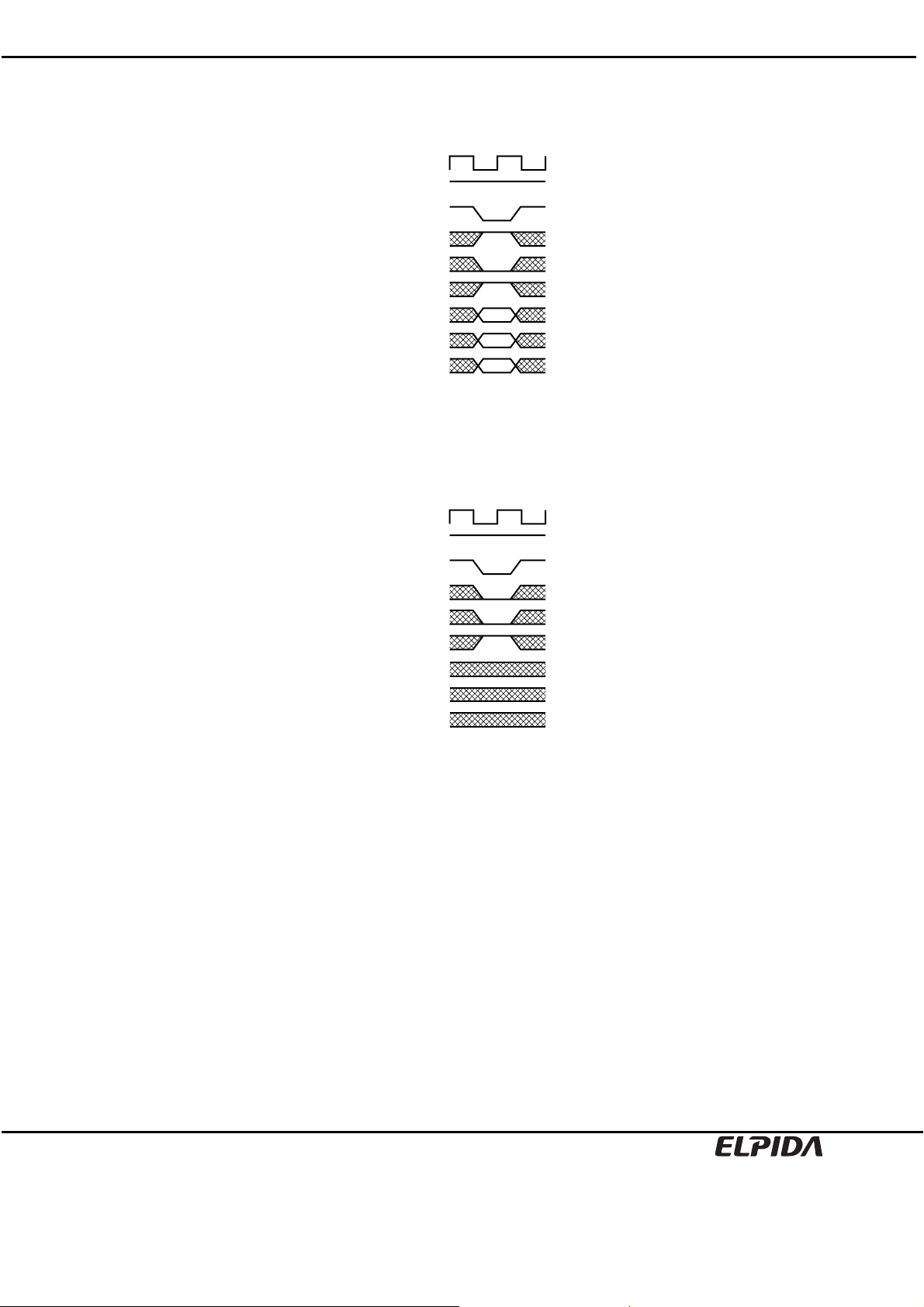
Read command (/CS, /CAS = Low, /RAS, /WE = High)
Read data is available after /CAS latency requirements have been met. This command sets the burst start address
given by the column address.
CLK
CKE
H
/CS
/RAS
/CAS
/WE
BA0, BA1
(Bank select)
A10
Add
Column Address and and Read Command
CBR (auto) refresh command (/CS, /RAS, /CAS = Low, /WE, CKE = High)
This command is a request to begin the CBR (auto) refresh operation. The refresh address is generated internally.
Before executing CBR (auto) refresh, all banks must be precharged. After this cycle, all banks will be in the idle
(precharged) state and ready for a row activate command. During tRC period (from refresh command to refresh or
activate command), the Synchronous DRAM cannot accept any other command
Col.
CLK
CKE
H
/CS
/RAS
/CAS
/WE
BA0, BA1
(Bank select)
A10
Add
CBR (auto) Refresh Command
Preliminary Data Sheet E0247E40 (Ver. 4.0)
14
EDS1232CABB, EDS1232CATA
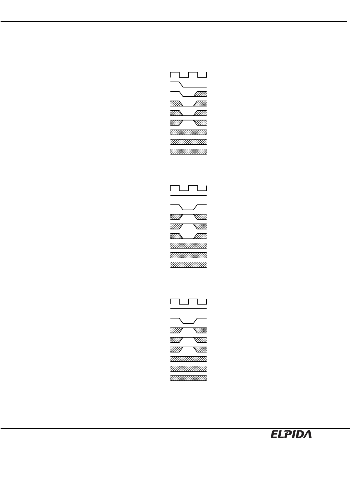
Self refresh entry command (/CS, /RAS, /CAS, CKE = Low, /WE = High)
After the command execution, self refresh operation continues while CKE remains low. When CKE goes high, the
Synchronous DRAM exits the self refresh mode. During self refresh mode, refresh interval and refresh operation are
performed internally, so there is no need for external control. Before executing self refresh, all banks must be
precharged.
CLK
CKE
/CS
/RAS
/CAS
/WE
BA0, BA1
(Bank select)
A10
Add
Self Refresh Entry Command
Burst stop command (/CS = /WE = Low, /RAS, /CAS = High)
This command can stop the current burst operation.
CLK
CKE
H
/CS
/RAS
/CAS
/WE
BA0, BA1
(Bank select)
A10
Add
Burst Stop Command in Full Page Mode
No operation (/CS = Low, /RAS, /CAS, /WE = High)
This command is not an execution command. No operations begin or terminate by this command.
CLK
CKE
H
/CS
/RAS
/CAS
/WE
BA0, BA1
(Bank select)
A10
Add
No Operation
Preliminary Data Sheet E0247E40 (Ver. 4.0)
15

EDS1232CABB, EDS1232CATA
Truth Table
Command Truth Table
CKE BA0, A9 - A0,
Function Symbol n – 1 n /CS /RAS /CAS /WE BA1 A10 A11
Device deselect DESL H × H × × × × × ×
No operation NOP H × L H H H × × ×
Burst stop BST H × L H H L × × ×
Read READ H × L H L H V L V
Read with auto precharge READA H × L H L H V H V
Write WRIT H × L H L L V L V
Write with auto precharge WRITA H × L H L L V H V
Bank activate ACT H × L L H H V V V
Precharge select bank PRE H × L L H L V L ×
Precharge all banks PALL H × L L H L × H ×
Mode register set MRS H × L L L L L L V
Remark: H: VIH. L: VIL. ×: VIH or VIL, V = Valid data
DQM Truth Table
CKE DQM
Function Symbol n – 1 n
Data write / output enable ENB H × L L L L
Data mask / output disable MASK H × H H H H
DQ0 to DQ7 write enable/output enable ENB0 H × L × × ×
DQ8 to DQ15 write enable/output enable ENB1 H × × L × ×
DQ16 to DQ23 write enable/output enable ENB2 H × × × L ×
DQ24 to DQ31 write enable/output enable ENB3 H × × × × L
DQ0 to DQ7 write inhibit/output disable MASK0 H × H × × ×
DQ8 to DQ15 write inhibit/output disable MASK 1 H × × H × ×
DQ16 to DQ23 write inhibit/output disable MASK 2 H × × × H ×
DQ24 to DQ31 write inhibit/output disable MASK 3 H × × × × H
0 1 2 3
Remark: H: VIH. L: VIL. ×: VIH or VIL
Preliminary Data Sheet E0247E40 (Ver. 4.0)
16

EDS1232CABB, EDS1232CATA
CKE Truth Table
CKE
Current state Function Symbol n – 1 n /CS /RAS /CAS /WE Address
Activating Clock suspend mode entry H L × × × × ×
Any Clock suspend mode L L × × × × ×
Clock suspend Cloc k suspend mode exit L H × × × × ×
Idle CBR (auto) refresh command REF H H L L L H ×
Idle Self refresh entry SELF H L L L L H
Self refresh Self refresh exit L H L H H H ×
L H H × × × ×
Idle Power down entry H L L H H H ×
H L H × × × ×
Power down Power down exit L H H × × × ×
L H L H H H ×
Remark: H: VIH. L: VIL. ×: VIH or VIL
×
Preliminary Data Sheet E0247E40 (Ver. 4.0)
17
 Loading...