ELPID EDL1216AASA-75-E Datasheet
DATA SHEET
128M bits Mobile RAM
EDL1216AASA (8M words ×××× 16 bits)
Description
The EDL1216AA is a 128M bits Mobile RAM organized
as 2,097,152 words × 16 bits × 4 banks. The Mobile
RAM achieved low power consumption and high-speed
data transfer using the pipeline architecture. All inputs
and outputs are synchronized with the positive edge of
the clock.
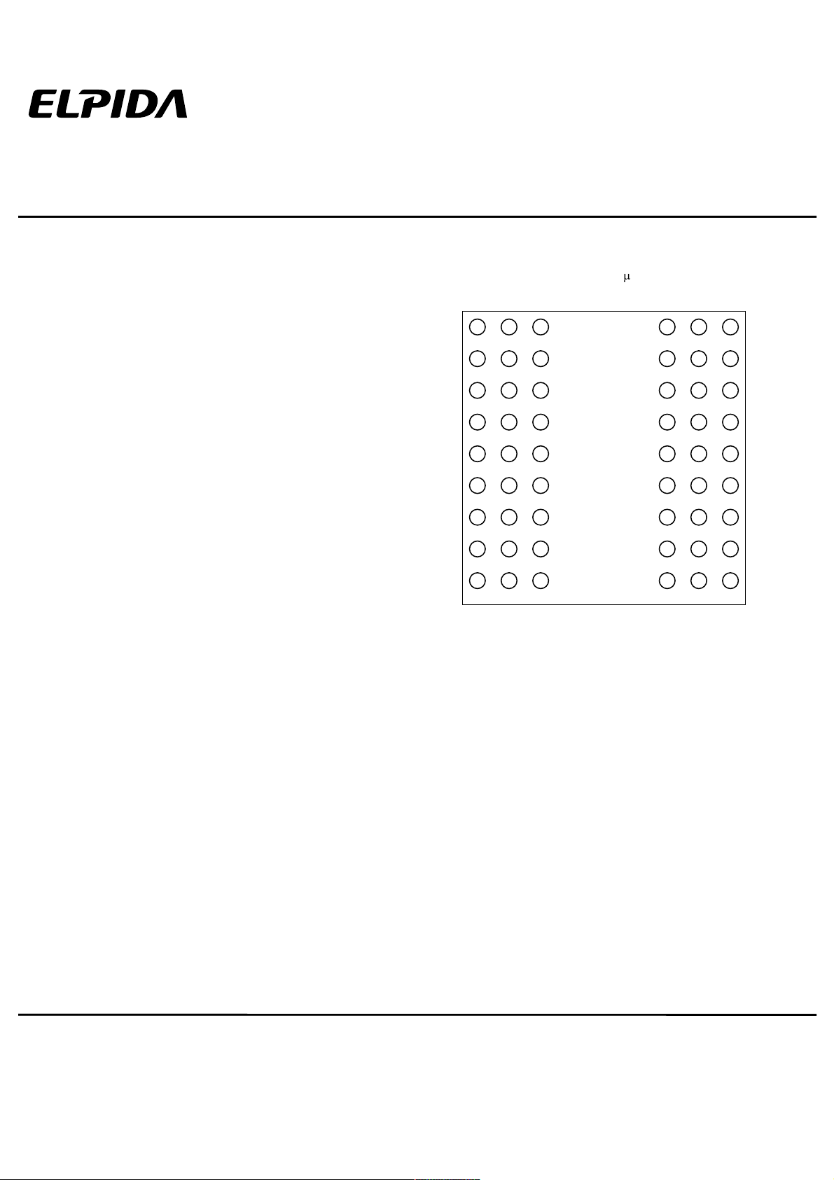
This product is packaged in 54-ball FBGA (µBGA
).
Features
• Low voltage power supply
VDD: 2.5V ± 0.2V
VDDQ: 1.8V ± 0.15V
• Wide temperature range (−25°C to 85°C)
• Programmable partial self refresh
• Programmable driver strength
• Programmable temperature compensated self refresh
(Option)
• Deep power down mode
• Small package (54-ball FBGA (µBGA))
• Fully Synchronous Dynamic RAM, with all signals
referenced to a positive clock edge
• Pulsed interface
• Possible to assert random column address in every
cycle
• Quad internal banks controlled by BA0 and BA1
• Byte control by LDQM and UDQM
• Wrap sequence = Sequential/ Interleave
• /CAS latency (CL) = 2, 3
• Automatic precharge and controlled precharge
• Auto refresh and self refresh
• ×16 organization
• 4,096 refresh cycles/64ms
• Burst termination by Burst stop command and
Precharge command
• FBGA(µBGA) package is lead free solder (Sn-Ag-Cu)
Applications
Mobile cellular handsets, PDAs, wireless PDAs,
handheld PCs, home electronic appliances, and
information appliances, etc.
Pin Configurations
/xxx indicates active low signal.
54-ball FBGA (
1
23456789
A
VSS
DQ15
VSSQ
B
DQ14
DQ13
VDDQ
C
DQ12
DQ11
VSSQ
D
DQ10
DQ9
VDDQ
E
DQ8
NC
VSS
F
UDQM
CLK
CKE
G
NC
A11
A9
H
A8
A7
A6
J
VSS
A5
A4
(Top view)
A0 to A11 Address inputs
BA0, BA1 Bank select
DQ0 to DQ15 Data inputs/ outputs
CLK Clock input
CKE Clock enable
/CS Chip select
/RAS Row address strobe
/CAS Column address strobe
/WE Write enable
UDQM Upper DQ mask enable
LDQM Lower DQ mask enable
VDD Power supply
VSS Ground
VDDQ Power supply for DQ
VSSQ Ground for DQ
NC No connection
BGA)
VDDQ
VSSQ
VDDQ
VSSQ
VDD
/CAS
BA0
A0
A3
DQ0
DQ2
DQ4
DQ6
LDQM
/RAS
BA1
A1
A2
VDD
DQ1
DQ3
DQ5
DQ7
/WE
/CS
A10
VDD
Document No. E0196E30 (Ver. 3.0)
Date Published June 2002 (K) Japan
URL: http://www.elpida.com
Elpida Memory, Inc. 2001-2002

EDL1216AASA
Ordering Information
Part number
EDL1216AASA-75-E 8M × 16 4 133 3 54-ball FBGA (µBGA)
Part Number
Organization
(words × bits)
Internal Banks
Clock frequency
MHz (max.)
/CAS latency Package
E D L 12 16 A A SA - 75 - E
Elpida Memory
Type
D: Monolithic Device
Product Code
L: Mobile RAM
Lead Free
Density / Bank
12: 128M / 4 banks
Bit Organization
16: x16
Voltage, Interface
A: VDD = 2.5V, VDDQ = 1.8V, LVCMOS
Speed
75: 133MHz
Package
SA: µBGA
Die Rev.
Data Sheet E0196E30 (Ver. 3.0)
2

EDL1216AASA
CONTENTS
Description .................................................................................................................................................... 1
Features ........................................................................................................................................................1
Applications ................................................................................................................................................... 1
Pin Configurations ......................................................................................................................................... 1
Ordering Information .....................................................................................................................................2
Electrical Specifications................................................................................................................................. 4
Pin Function .................................................................................................................................................. 9
Command Operation ................................................................................................................................... 10
Truth Table .................................................................................................................................................. 14
Simplified State Diagram............................................................................................................................. 19
Initialization.................................................................................................................................................. 20
Programming Mode Registers .................................................................................................................... 20
Address Bits of Bank-Select and Precharge ............................................................................................... 24
Operation of the Mobile RAM...................................................................................................................... 25
Timing Waveforms ...................................................................................................................................... 33
Package Drawing ........................................................................................................................................56
Recommended Soldering Conditions.......................................................................................................... 57
Revision History .......................................................................................................................................... 60
Data Sheet E0196E30 (Ver. 3.0)
3

EDL1216AASA
Electrical Specifications
• All voltages are referenced to VSS (GND).
• After power up, wait more than 200 µs and then, execute Power on sequence and two Auto Refresh before proper
device operation is achieved.
Absolute Maximum Ratings
Parameter Symbol Rating Unit Note
Voltage on any pin relative to VSS VT –0.5 to +3.6 V
Supply voltage relative to VSS VDD, VDDQ –0.5 to +3.6 V
Short circuit output current IOS 50 mA
Power dissipation PD 1.0 W
Operating ambient temperature TA –25 to +85 °C
Storage temperature Tstg –55 to +125 °C
Caution
Exposing the device to stress above those listed in Absolute Maximum Ratings could cause
permanent damage. The device is not meant to be operated under conditions outside the limits
described in the operational section of this specification. Exposure to Absolute Maximum Rating
conditions for extended periods may affect device reliability.
Recommended Operating Conditions (TA = –25 to +85°°°°C)
Parameter Symbol min. typ. max. Unit Notes
Supply voltage VDD 2.3 2.5 2.7 V
VSS 0 0 0 V
DQ Supply voltage VDDQ 1.65 1.8 1.95 V
Input high voltage VIH 0.8 × VDDQ VDDQ + 0.3*
Input low voltage VIL –0.3*
2
0.3 V
1
V
Notes: 1. VIH (max.) = VDDQ + 1.5V (pulse width ≤ 5ns).
2. VIL (min.) = –1.5V (pulse width ≤ 5ns).
Data Sheet E0196E30 (Ver. 3.0)
4

EDL1216AASA
DC Characteristics (TA = –25 to +85°°°°C, VDD = 2.5V ± 0.2V, VDDQ = 1.8V ± 0.15V, VSS, VSSQ = 0V)
Parameter
/CAS latency Symbol Grade max. Unit Test condition Notes
Operating current
(CL = 2)
(CL = 3) IDD1 65 mA
Standby current in power down IDD2P 1 mA CKE ≤ VIL max., tCK = 15ns
Standby current in power down
(input signal stable)
Standby current in non power
down
Standby current in non power
down (input signal stable)
Active standby current in power
down
Active standby current in power
down (input signal stable)
Active standby current in non
power down
Active standby current in non
power down (input signal stable)
Burst operating current
(CL = 2)
(CL = 3) IDD4 80 mA
Refresh current
(CL = 2)
(CL = 3) IDD5 155 mA
Self refresh current
PASR="000" (Full)
PASR="001" (2BK) 0.25 mA CKE ≤ 0.2V
PASR="010" (1BK) 0.18 mA
PASR="101" (1/2 BK) 0.12 mA
PASR="110" (1/4 BK) 0.09 mA
PASR="000" (Full) IDD6 0.20 mA TCSR="01" (Ts*
PASR="001" (2BK) 0.15 mA CKE ≤ 0.2V
PASR="010" (1BK) 0.10 mA
PASR="101" (1/2 BK) 0.08 mA
PASR="110" (1/4 BK) 0.07 mA
PASR="000" (Full) IDD6 0.60 mA TCSR="11" (Ts*
PASR="001" (2BK) 0.50 mA CKE ≤ 0.2V
PASR="010" (1BK) 0.43 mA
PASR="101" (1/2 BK) 0.37 mA
PASR="110" (1/4 BK) 0.34 mA
Standby current in deep power
down mode
IDD1 65 mA 1
IDD2PS 0.6 mA CKE ≤ VIL max., tCK = ∞
IDD2N 5.5 mA
IDD2NS 2 mA
IDD3P 1.5 mA
IDD3PS 1 mA
IDD3N 17 mA
IDD3NS 12 mA
IDD4 60 mA
IDD5 155 mA tRC ≥ tRC min. 3
IDD6 0.35 mA TCSR="00" (Ts*
IDD7 10 µA CKE ≤ 0.2V
Burst length = 1
tRC ≥ tRC min., IO = 0mA,
One bank active
CKE ≥ VIH min., tCK = 15ns,
/CS ≥ VIH min.,
Input signals are changed one
time during 30ns.
CKE ≥ VIH min., tCK = ∞,
Input signals are stable.
CKE ≤ VIL max., tCK = 15ns
CKE ≤ VIL max., tCK = ∞
CKE ≥ VIH min., tCK = 15 ns,
/CS ≥ VIH min.,
Input signals are changed one
time during 30ns.
CKE ≥ VIH min., tCK = ∞,
Input signals are stable.
tCK ≥ tCK min.,
IOUT = 0mA, All banks active
4
≤ 70°C)
4
≤ 45°C)
4
≤ 85°C)
2
Data Sheet E0196E30 (Ver. 3.0)
5

EDL1216AASA
Notes: 1. IDD1 depends on output loading and cycle rates. Specified values are obtained with the output open. In
addition to this, IDD1 is measured condition that addresses are changed only one time during tCK (min.).
2. IDD4 depends on output loading and cycle rates. Specified values are obtained with the output open. In
addition to this, IDD4 is measured condition that addresses are changed only one time during tCK (min.).
3. IDD5 is measured on condition that addresses are changed only one time during tCK (min.).
4. Ts is surface temperature.
DC Characteristics 2 (TA = –25 to +85°°°°C, VDD = 2.5V ± 0.2V, VDDQ = 1.8V ± 0.15V, VSS, VSSQ = 0V)
Parameter Symbol min. max. Unit Test condition Notes
Input leakage current ILI –1.0 1.0 µA 0 ≤ VIN ≤ VDDQ
Output leakage current ILO –1.5 1.5 µA 0 ≤ VOUT ≤ VDDQ, DQ = disable
Output high voltage VOH VDDQ – 0.2 — V IOH = –0.1 mA
Output low voltage VOL — 0.2 V IOL = 0.1 mA
Pin Capacitance (TA = 25°C, f = 1MHz)
Parameter Symbol Pins min. Typ max. Unit
Input capacitance CI1 CLK 2.0 — 3.5 pF
CI2
Data input/output capacitance CI/O DQ 4 — 6.5 pF
Address, CKE, /CS, /RAS,
/CAS, /WE, UDQM, LDQM
2.0 — 3.8 pF
Notes
Data Sheet E0196E30 (Ver. 3.0)
6
EDL1216AASA
AC Characteristics (TA = –25 to +85°°°°C, VDD = 2.5V ± 0.2V, VDDQ = 1.8V ± 0.15V, VSS, VSSQ = 0V)
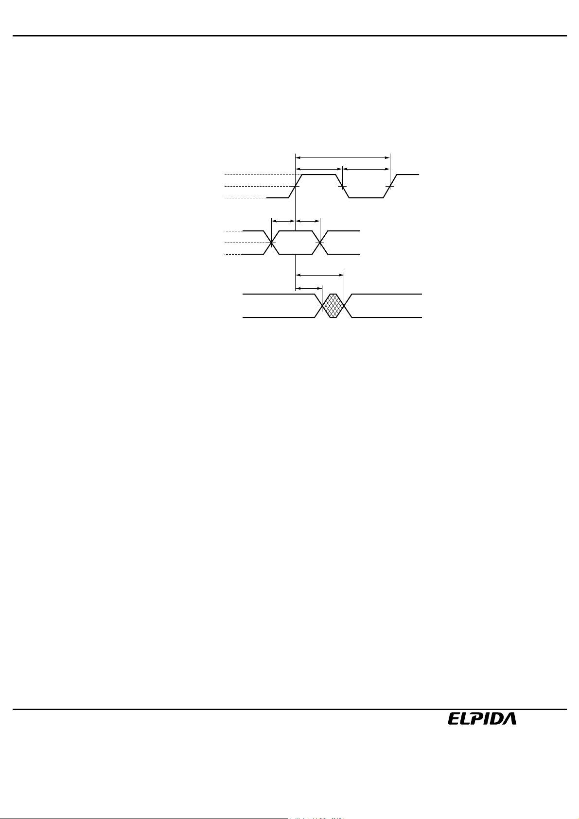
Test Conditions
• AC high level input voltage / low level input voltage: 1.6 / 0.2V
• Input timing measurement reference level: 0.9V
• Transition time (Input rise and fall time): 1ns
• Output timing measurement reference level: 0.9V
t
CK
t
CLK
Input
1.6 V
0.9 V
0.2 V
1.6 V
0.9 V
0.2 V
t
SETUPtHOLD
CH
t
AC
t
OH
t
CL
Output
Data Sheet E0196E30 (Ver. 3.0)
7
EDL1216AASA
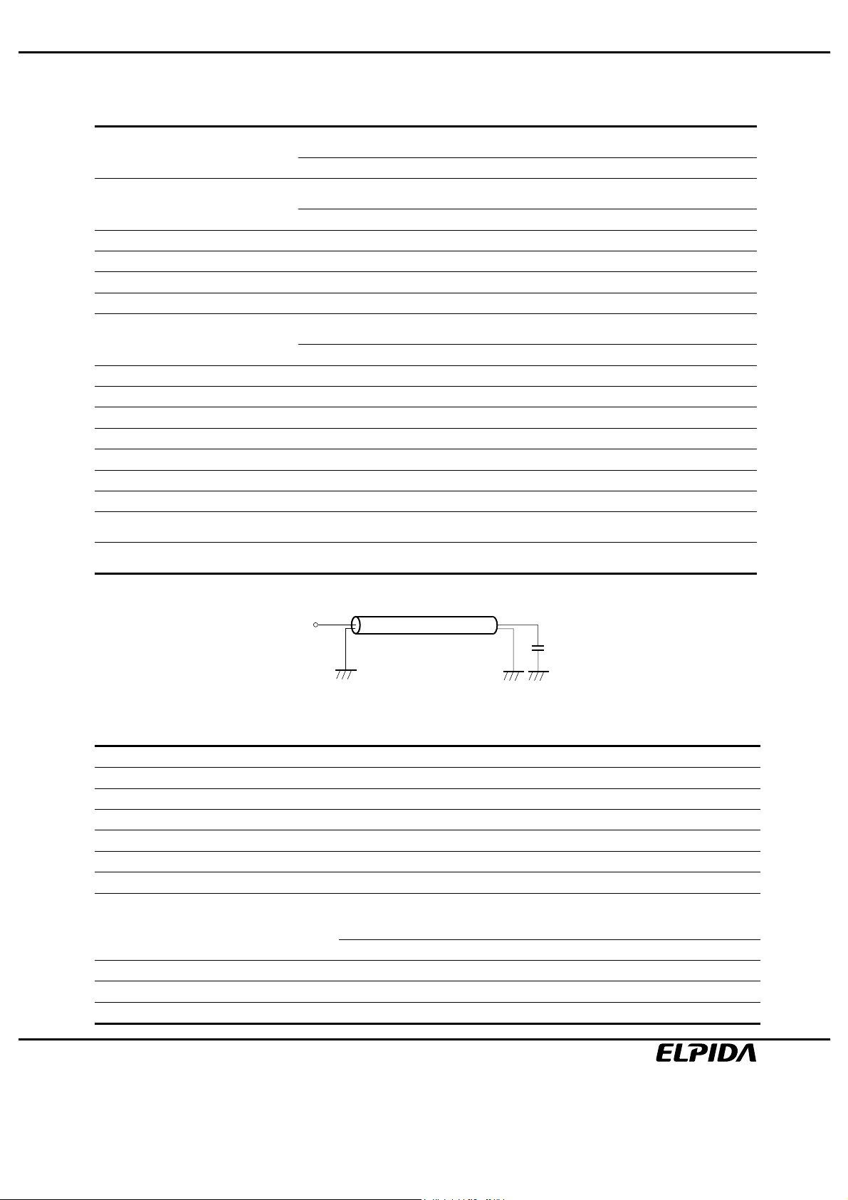
Synchronous Characteristics
Parameter Symbol min. max. Unit Note
Clock cycle time
(CL= 2)
(CL= 3) tCK3 7.5 — ns
Access time from CLK
(CL= 2)
(CL= 3) tAC3 — 5.4 ns 1
CLK high level width tCH 2.5 — ns
CLK low level width tCL 2.5 — ns
Data-out hold time tOH 2.5 — ns 1
Data-out low-impedance time tLZ 0 — ns
Data-out high-impedance time
(CL= 2)
(CL= 3) tHZ3 2.5 5.4 ns
Data-in setup time tDS 1.5 — ns
Data-in hold time tDH 0.8 — ns
Address setup time tAS 1.5 — ns
Address hold time tAH 0.8 — ns
CKE setup time tCKS 1.5 — ns
CKE hold time tCKH 0.8 — ns
CKE setup time (Power down exit) tCKSP 1.5 — ns
Command (/CS, /RAS, /CAS, /WE,
UDQM, LDQM) setup time
Command (/CS, /RAS, /CAS, /WE,
UDQM, LDQM) hold time
Note: 1. Output load.
tCK2 10 — ns
tAC2 — 6 ns 1
tHZ2 2.5 6 ns
tCMS 1.5 — ns
tCMH 0.8 — ns
Z = 50 Ω
Output
30 pF
Output load
Asynchronous Characteristics
Parameter Symbol min. max. Unit Notes
ACT to REF/ACT command period (operation) tRC 67.5 ns
ACT to REF/ACT command period (refresh) tRC1 67.5 ns
ACT to PRE command period tRAS 45 120000 ns
PRE to ACT command period tRP 20
Delay time ACT to READ/WRITE command tRCD 20
ACT (one) to ACT (another) command period tRRD 15
Data-in to PRE command period tDPL 15
Data-in to ACT (REF) command period
(Auto precharge)
(CL = 2)
(CL = 3) TDAL3 2CLK + 20
Mode register set cycle time tRSC 2
Transition time tT 0.5 30 ns
Refresh time (4,096 refresh cycles) tREF 64 ms
TDAL2 2CLK + 20
ns
ns
ns
ns
ns
ns
CLK
Data Sheet E0196E30 (Ver. 3.0)
8

EDL1216AASA
Pin Function
CLK (input pin)
CLK is the master clock input. Other inputs signals are referenced to the CLK rising edge.
CKE (input pins)
CKE determine validity of the next CLK (clock). If CKE is high, the next CLK rising edge is valid; otherwise it is
invalid. If the CLK rising edge is invalid, the internal clock is not issued and the Mobile RAM suspends operation.
When the Mobile RAM is not in burst mode and CKE is negated, the device enters power down mode. During power
down mode, CKE must remain low.
/CS (input pins)
/CS low starts the command input cycle. When /CS is high, commands are ignored but operations continue.
/RAS, /CAS, and /WE (input pins)
/RAS, /CAS and /WE have the same symbols on conventional DRAM but different functions. For details, refer to the
command table.
A0 to A11 (input pins)
Row Address is determined by A0 to A11 at the CLK (clock) rising edge in the active command cycle. It does not
depend on the bit organization.
Column Address is determined by A0 to 8 at the CLK rising edge in the read or write command cycle.
A10 defines the precharge mode. When A10 is high in the precharge command cycle, all banks are precharged;
when A10 is low, only the bank selected by BA0 and BA1 is precharged.
When A10 is high in read or write command cycle, the precharge starts automatically after the burst access.
BA0 and BA1 (input pin)
BA0 and BA1 are bank select signal. (See Bank Select Signal Table)
[Bank Select Signal Table]
BA0 BA1
Bank A L L
Bank B H L
Bank C L H
Bank D H H
Remark: H: VIH. L: VIL. ×: VIH or VIL
UDQM and LDQM (input pins)
UDQM and LDQM control upper byte and lower byte I/O buffers, respectively. In read mode, DQM controls the
output buffers like a conventional /OE pin. DQM high and DQM low turn the output buffers off and on, respectively.
The DQM latency for the read is two clocks. In write mode, DQM controls the word mask. Input data is written to the
memory cell if DQM is low but not if DQM is high. The DQM latency for the write is zero.
DQ0 to DQ15 (input/output pins)
DQ pins have the same function as I/O pins on a conventional DRAM.
VDD, VSS, VDDQ, VSSQ (Power supply)
VDD and VSS are power supply pins for internal circuits. VDDQ and VSSQ are power supply pins for the output
buffers.
Data Sheet E0196E30 (Ver. 3.0)
9
EDL1216AASA
Command Operation
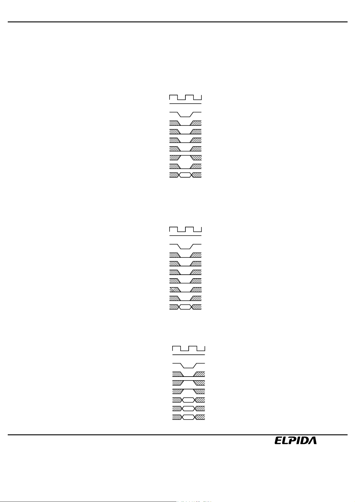
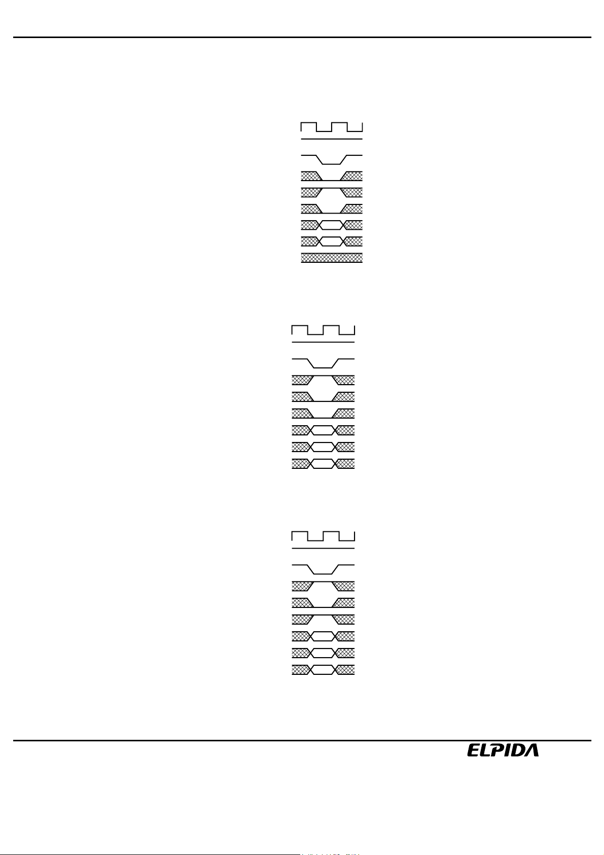
Extended Mode register set command (/CS, /RAS, /CAS, /WE, BA0 = Low, BA1 = High)
The Mobile RAM has an extended mode register that defines low power functions. In this command, A0 through A11
are the data input pins.
After power on, the extended mode register set command must be executed to fix low power functions.
The extended mode register can be set only when all banks are in idle state.
During tRSC following this command, the Mobile RAM can not accept any other commands.
CLK
CKE
H
/CS
/RAS
/CAS
/WE
BA0
BA1
A10
Add
Extended Mode register set command
Mode register set command (/CS, /RAS, /CAS, /WE, BA0, BA1 = Low)
The Mobile RAM has a mode register that defines how the device operates. In this command, A0 through A11 are
the data input pins. After power on, the mode register set command must be executed to initialize the device. The
mode register can be set only when all banks are in idle state. During tRSC following this command, the Mobile
RAM cannot accept any other commands.
CLK
CKE
H
/CS
/RAS
/CAS
/WE
BA0
BA1
A10
Add
Mode register set command
Activate command (/CS, /RAS = Low, /CAS, /WE = High)
The Mobile RAM has four banks, each with 4,096 rows. This command activates the bank selected by BA0 and BA1
and a row address selected by A0 through A11. This command corresponds to a conventional DRAM's /RAS falling.
CLK
CKE
H
/CS
/RAS
/CAS
/WE
BA0, BA1
A10
Add
Row
Row
Activate command
Data Sheet E0196E30 (Ver. 3.0)
10
EDL1216AASA
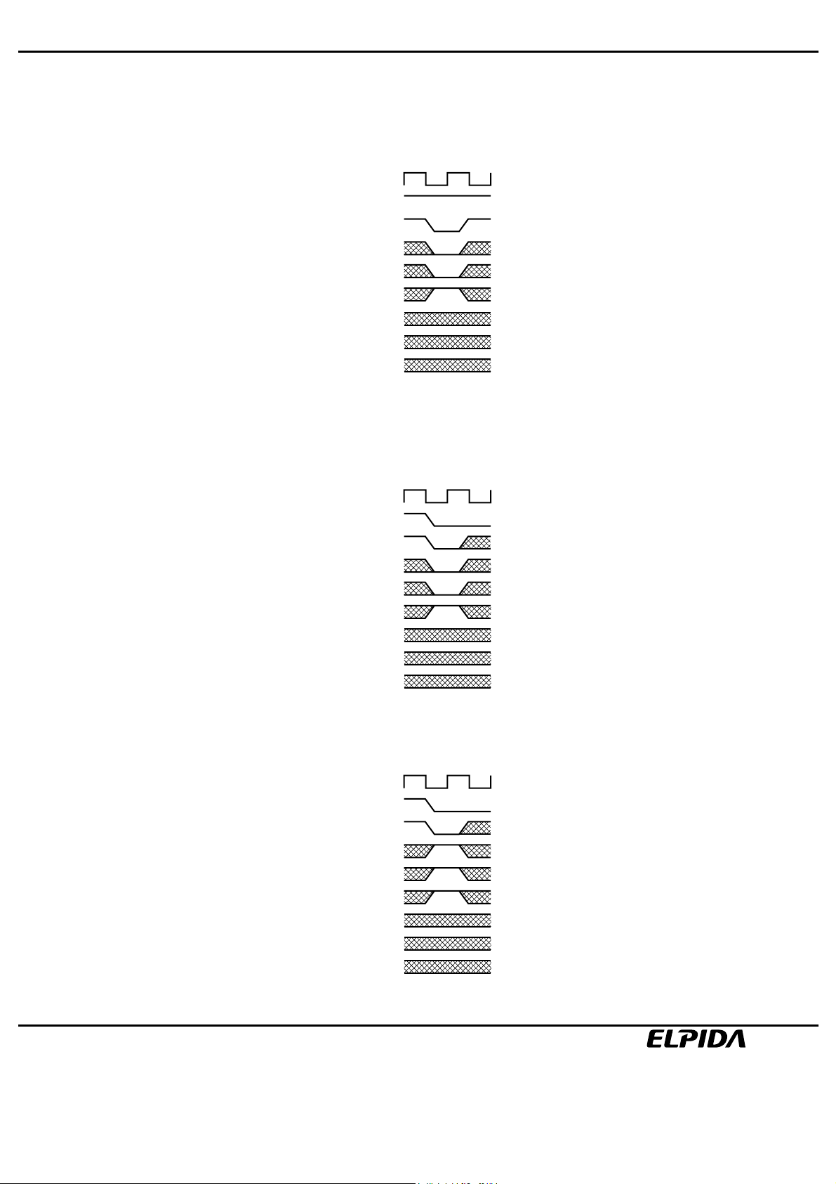
Precharge command (/CS, /RAS, /WE = Low, /CAS = High)
This command begins precharge operation of the bank selected by BA0 and BA1. When A10 is High, all banks are
precharged, regardless of BA0 and BA1. When A10 is Low, only the bank selected by BA0 and BA1 is precharged.
After this command, the Mobile RAM can’t accept the activate command to the precharging bank during tRP
(precharge to activate command period). This command corresponds to a conventional DRAM’s /RAS rising.
CLK
CKE
H
/CS
/RAS
/CAS
/WE
BA0, BA1
(Precharge select)
Write command (/CS, /CAS, /WE = Low, /RAS = High)
This command sets the burst start address given by the column address to begin the burst write operation. The first
write data in burst mode can input with this command with subsequent data on following clocks.
A10
Add
Precharge command
CLK
CKE
H
/CS
/RAS
/CAS
/WE
BA0, BA1
A10
Add
Col.
Write command
Read command (/CS, /CAS = Low, /RAS, /WE = High)
Read data is available after /CAS latency requirements have been met. This command sets the burst start address
given by the column address.
CLK
CKE
H
/CS
/RAS
/CAS
/WE
BA0, BA1
A10
Add
Col.
Read command
Data Sheet E0196E30 (Ver. 3.0)
11
EDL1216AASA
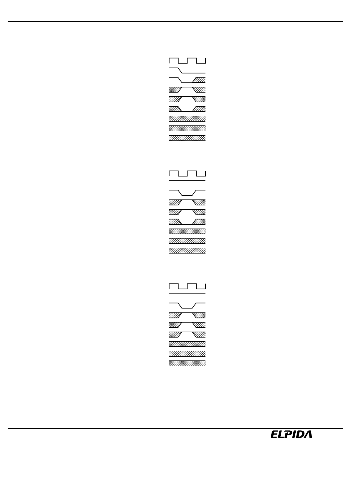
Auto refresh command (/CS, /RAS, /CAS = Low, /WE, CKE = High)
This command is a request to begin the Auto refresh operation. The refresh address is generated internally.
Before executing Auto refresh, all banks must be precharged. After this cycle, all banks will be in the idle
(precharged) state and ready for a row activate command. During tRC1 period (from refresh command to refresh or
activate command), the Mobile RAM cannot accept any other command
CLK
CKE
H
/CS
/RAS
/CAS
/WE
BA0, BA1
A10
Add
Auto refresh command
Self refresh entry command (/CS, /RAS, /CAS, CKE = Low, /WE = High)
After the command execution, self refresh operation continues while CKE remains low. When CKE goes high, the
Mobile RAM exits the self refresh mode. During self refresh mode, refresh interval and refresh operation are
performed internally, so there is no need for external control. Before executing self refresh, all banks must be
precharged.
CLK
CKE
/CS
/RAS
/CAS
/WE
BA0, BA1
A10
Add
Self refresh entry command
Power down entry command (/CS, CKE = Low, /RAS, /CAS, /WE = High)
After the command execution, power down mode continues while CKE remains low. When CKE goes high, the
Mobile RAM exits the power down mode. Before executing power down, all banks must be precharged.
CLK
CKE
/CS
/RAS
/CAS
/WE
BA0, BA1
A10
Add
Power down entry command
Data Sheet E0196E30 (Ver. 3.0)
12
EDL1216AASA
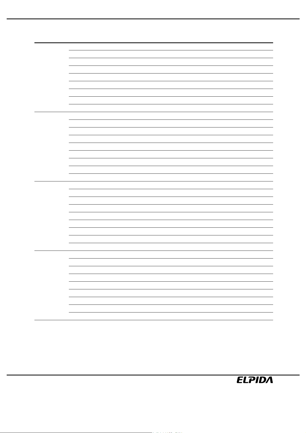
Deep power down entry command( /CS, CKE, /WE = Low, /RAS, /CAS = High)
After the command execution, deep power down mode continues while CKE remains low. When CKE goes high, the
Mobile RAM exits the deep power down mode. Before executing deep power down, all banks must be precharged.
CLK
CKE
/CS
/RAS
/CAS
/WE
BA0, BA1
A10
Add
Deep power down entry command
Burst stop command (/CS = /WE = Low, /RAS, /CAS = High)
This command can stop the current burst operation.
CLK
CKE
H
/CS
/RAS
/CAS
/WE
BA0, BA1
A10
Add
Burst stop command
No operation (/CS = Low, /RAS, /CAS, /WE = High)
This command is not an execution command. No operations begin or terminate by this command.
CLK
CKE
H
/CS
/RAS
/CAS
/WE
BA0, BA1
A10
Add
No operation
Data Sheet E0196E30 (Ver. 3.0)
13

EDL1216AASA
Truth Table
Command Truth Table
CKE A11,
Function Symbol n – 1 n /CS /RAS /CAS /WE BA1 BA0 A10 A9 - A0
Device deselect DESL H × H × × × × × × ×
No operation NOP H × L H H H × × × ×
Burst stop BST H H L H H L × × × ×
Read READ H × L H L H V V L V
Read with auto precharge READA H × L H L H V V H V
Write WRIT H × L H L L V V L V
Write with auto precharge WRITA H × L H L L V V H V
Bank activate ACT H × L L H H V V V V
Precharge select bank PRE H × L L H L V V L ×
Precharge all banks PALL H × L L H L × × H ×
Mode register set MRS H × L L L L L L L V
Extended mode register set EMRS H × L L L L H L L V
Remark: H: VIH. L: VIL. ×: VIH or VIL, V = Valid data
DQM Truth Table
CKE DQM
Function Symbol n – 1 n U L
Data write / output enable ENB H × L L
Data mask / output disable MASK H × H H
Upper byte write enable / output enable ENBU H × L ×
Lower byte write enable / output enable ENBL H × × L
Upper byte write inhibit / output disable MASKU H × H ×
Lower byte write inhibit / output disable MASKL H × × H
Remark: H: VIH. L: VIL. ×: VIH or VIL
CKE Truth Table
CKE
Current state Function Symbol n – 1 n /CS /RAS /CAS /WE Address
Activating Clock suspend mode entry H L × × × × ×
Any Clock suspend mode L L × × × × ×
Clock suspend Clock suspend mode exit L H × × × × ×
Idle Auto refresh command REF H H L L L H ×
Idle Self refresh entry SELF H L L L L H
Idle Power down entry PD H L L H H H ×
H L H × × × ×
Idle Deep power down entry DPD H L L H H L ×
Self refresh Self refresh exit L H L H H H ×
L H H × × × ×
Power down Power down exit L H L H H H ×
L H H × × × ×
Deep power down
Deep power down exit L H × × × × ×
×
Remark: H: VIH. L: VIL. ×: VIH or VIL
Data Sheet E0196E30 (Ver. 3.0)
14

EDL1216AASA
Function Truth Table
Current state /CS /RAS /CAS /WE Address Command Action Notes
Idle H × × × × DESL Nop
L H H H × NOP Nop
L H H L × BST Nop
L H L H BA, CA, A10
L H L L BA, CA, A10
L L H H BA, RA ACT → Row activating
L L H L BA, A10 PRE/PALL Nop
L L L H × REF Auto refresh
L L L L OC, BA1= L MRS Mode register set
L L L L OC, BA1= H EMRS Extended mode register set
Row active H × × × × DESL Nop
L H H H × NOP Nop
L H H L × BST Nop
L H L H BA, CA, A10
L H L L BA, CA, A10
L L H H BA, RA ACT ILLEGAL 2
L L H L BA, A10 PRE/PALL Precharge/Precharge all banks 4
L L L H × REF ILLEGAL
L L L L OC, BA MRS/EMRS ILLEGAL
Read H × × × × DESL Continue burst to end → Row active
L H H H × NOP Continue burst to end → Row active
L H H L × BST Burst stop → Row active
L H L H BA, CA, A10 READ/READA Terminate burst, begin new read 5
L H L L BA, CA, A10 WRIT/WRITA Terminate burst, begin write 5, 6
L L H H BA, RA ACT ILLEGAL 2
L L H L BA, A10 PRE/PALL Terminate burst → Precharging
L L L H × REF ILLEGAL
L L L L OC, BA MRS/EMRS ILLEGAL
Write H × × × × DESL Continue burst to end → Write recovering
L H H H × NOP Continue burst to end → W rite recovering
L H H L × BST Burst stop → Row active
L H L H BA, CA, A10 READ/READA Terminate burst, start read : Determine AP 5, 6
L H L L BA, CA, A10 WRIT/WRITA Terminate burst, new write : Determine AP 5
L L H H BA, RA ACT ILLEGAL 2
L L H L BA, A10 PRE/PALL Terminate burst → Precharging 7
L L L H × REF ILLEGAL
L L L L OC, BA MRS/EMRS ILLEGAL
READ/READA
WRIT/ WRITA
READ/READA
WRIT/ WRITA
ILLEGAL 2
ILLEGAL 2
Begin read 3
Begin write 3
Data Sheet E0196E30 (Ver. 3.0)
15

EDL1216AASA
Current state /CS /RAS /CAS /WE Address Command Action Notes
Read with auto
precharge L H H H × NOP Continue burst to end → Precharging
L H H L × BST ILLEGAL
L H L H BA, CA, A10
L H L L BA, CA, A10
L L H H BA, RA ACT ILLEGAL 2
L L H L BA, A10 PRE/PALL ILLEGAL 2
L L L H × REF ILLEGAL
L L L L OC, BA MRS/EMRS ILLEGAL
H × × × × DESL Continue burst to end → Precharging
READ/READA
WRIT/ WRITA
ILLEGAL 2
ILLEGAL 2
Write with auto
precharge
L H H H × NOP
L H H L × BST ILLEGAL
L H L H BA, CA, A10
L H L L BA, CA, A10
L L H H BA, RA ACT ILLEGAL 2
L L H L BA, A10 PRE/PALL ILLEGAL 2
L L L H × REF ILLEGAL
L L L L OC, BA MRS/EMRS ILLEGAL
Precharging H × × × × DESL Nop → Enter idle after tRP
L H H H × NOP Nop → Enter idle after tRP
L H H L × BST ILLEGAL
L H L H BA, CA, A10 READ/READA ILLEGAL 2
L H L L BA, CA, A10 WRIT/WRITA ILLEGAL 2
L L H H BA, RA ACT ILLEGAL 2
L L H L BA, A10 PRE/PALL Nop → Enter idle after tRP
L L L H × REF ILLEGAL
L L L L OC, BA MRS/EMRS ILLEGAL
Row activating
L H H H × NOP Nop → Enter bank active after tRCD
L H H L × BST ILLEGAL
L H L H BA, CA, A10 READ/READA ILLEGAL 2
L H L L BA, CA, A10 WRIT/WRITA ILLEGAL 2
L L H H BA, RA ACT ILLEGAL 2, 8
L L H L BA, A10 PRE/PALL ILLEGAL 2
L L L H × REF ILLEGAL
L L L L OC, BA MRS/EMRS ILLEGAL
H × × × × DESL
READ/READA
WRIT/ WRITA
H × × × × DESL Nop → Enter bank active after tRCD
Continue burst to end → Write recovering
with auto precharge
Continue burst to end → Write recovering
with auto precharge
ILLEGAL 2
ILLEGAL 2
Data Sheet E0196E30 (Ver. 3.0)
16
EDL1216AASA
Current state /CS /RAS /CAS /WE Address Command Action Notes
Write recovering
L H H H × NOP Nop → Enter row active after tDPL
L H H L × BST Nop → Enter row active after tDPL
L H L H BA, CA, A10
L H L L BA, CA, A10
L L H H BA, RA ACT ILLEGAL 2
L L H L BA, A10 PRE/PALL ILLEGAL 2
L L L H × REF ILLEGAL
L L L L OC, BA MRS/EMRS ILLEGAL
Write recovering
with auto L H H H × NOP Nop → Enter precharge after tDPL
precharge L H H L × BST Nop → Enter row active after tDPL
L H L H BA, CA, A10 READ/READA ILLEGAL
L H L L BA, CA, A10 WRIT/WRITA ILLEGAL 2, 6
L L H H BA, RA ACT ILLEGAL 2
L L H L BA, A10 PRE/PALL ILLEGAL 2
L L L H × REF ILLEGAL
L L L L OC, BA MRS/EMRS ILLEGAL
Refresh
L H H H × NOP Nop → Enter idle after tRC1
L H H L × BST Nop → Enter idle after tRC1
L H L H BA, CA, A10 READ/READA ILLEGAL
L H L L BA, CA, A10 WRIT/WRITA ILLEGAL
L L H H BA, RA ACT ILLEGAL
L L H L BA, A10 PRE/PALL ILLEGAL
L L L H × REF ILLEGAL
L L L L OC, BA MRS/EMRS ILLEGAL
Mode register
accessing L H H H × NOP Nop → Enter idle after tRSC
L H H L × BST Nop → Enter idle after tRSC
L H L L BA, CA, A10 WRIT/WRITA ILLEGAL
L L H H BA, RA ACT ILLEGAL
L L H L BA, A10 PRE/PALL ILLEGAL
L L L H × REF ILLEGAL
L L L L OC, BA MRS/EMRS ILLEGAL
H × × × × DESL Nop → Enter row active after tDPL
READ/READA
WRIT/ WRITA
H × × × × DESL Nop → Enter precharge after tDPL
H × × × × DESL Nop → Enter idle after tRC1
H × × × × DESL Nop → Enter idle after tRSC
L H L H BA, CA, A10 READ/READA ILLEGAL
Begin read 6
Begin new write
Data Sheet E0196E30 (Ver. 3.0)
17

EDL1216AASA
Current state /CS /RAS /CAS /WE Address Command Action Notes
Extended mode
register L H H H × NOP Nop → Enter idle after tRSC
accessing L H H L × BST Nop → Enter idle after tRSC
L H L H BA, CA, A10 READ/READA ILLEGAL
L H L L BA, CA, A10 WRIT/WRITA ILLEGAL
L L H H BA, RA ACT ILLEGAL
L L H L BA, A10 PRE/PALL ILLEGAL
L L L H × REF ILLEGAL
L L L L OC, BA0,BA1 MRS/EMRS ILLEGAL
Remark: H: VIH. L: VIL. ×: VIH or VIL, V = Valid data
Notes: 1. All entries assume that CKE is active (CKE
2. Illegal to bank in specified states; Function may be legal in the bank indicated by Bank Address (BA),
3. Illegal if tRCD is not satisfied.
4. Illegal if tRAS is not satisfied.
5. Must satisfy burst interrupt condition.
6. Must satisfy bus contention, bus turn around, and/or write recovery requirements.
7. Must mask preceding data which don't satisfy tDPL.
8. Illegal if tRRD is not satisfied.
H × × × × DESL Nop → Enter idle after tRSC
BA: Bank Address, CA: Column Address, RA: Row Address, OC: Op-Code
=CKEn=H).
n-1
depending on the state of that bank.
Data Sheet E0196E30 (Ver. 3.0)
18
 Loading...