ELPID EDE5104GBSA-5A-E, EDE5104GBSA-4A-E, EDE5116GBSA-5A-E, EDE5116GBSA-4A-E, EDE5108GBSA-5A-E Datasheet
...
PRELIMINARY DATA SHEET
512M bits DDR-II SDRAM
EDE5104GBSA (128M words ×××× 4 bits)
EDE5108GBSA (64M words ×××× 8 bits)
EDE5116GBSA (32M words ×××× 16 bits)
Description
The EDE5104GB is a 512M bits DDR-II SDRAM
organized as 33,554,432 words × 4 bits × 4 banks.
The EDE5108GB is a 512M bits DDR-II SDRAM
organized as 16,777,216 words × 8 bits × 4 banks.
It packaged in 64-ball µBGA
The EDE5116GB is a 512M bits DDR-II SDRAM
organized as 8,388,608 words × 16 bits × 4 banks.
It is packaged in 84-ball µBGA package.
package.
Features
• 1.8V power supply
• Double-data-rate architecture: two data transfers per
clock cycle
• Bi-directional, differential data strobe (DQS and
/DQS) is transmitted/received with data, to be used in
capturing data at the receiver
• DQS is edge aligned with data for READs: centeraligned with data for WRITEs
• Differential clock inputs (CK and /CK)
• DLL aligns DQ and DQS transitions with CK
transitions
• Commands entered on each positive CK edge: data
and data mask referenced to both edges of DQS
• Four internal banks for concurrent operation
• Data mask (DM) for write data
• Burst lengths: 4, 8
• /CAS Latency (CL): 3, 4, 5
• Auto precharge operation for each burst access
• Auto refresh and self refresh modes
• 7.8µs average periodic refresh interval
• 1.8V (SSTL_18 compatible) I/O
• Posted CAS by programmable additive latency for
better command and data bus efficiency
• Off-Chip-Driver Impedance Adjustment and On-DieTermination for better signal quality
• Programmable RDQS, /RDQS output for making × 8
organization compatible to × 4 organization
• /DQS, (/RDQS) can be disabled for single-ended
Data Strobe operation.
• µBGA package is lead free solder (Sn-Ag-Cu)
Document No. E0249E30 (Ver. 3.0)
Date Published August 2002 (K) Japan
URL: http://www.elpida.com
Elpida Memory, Inc. 2002
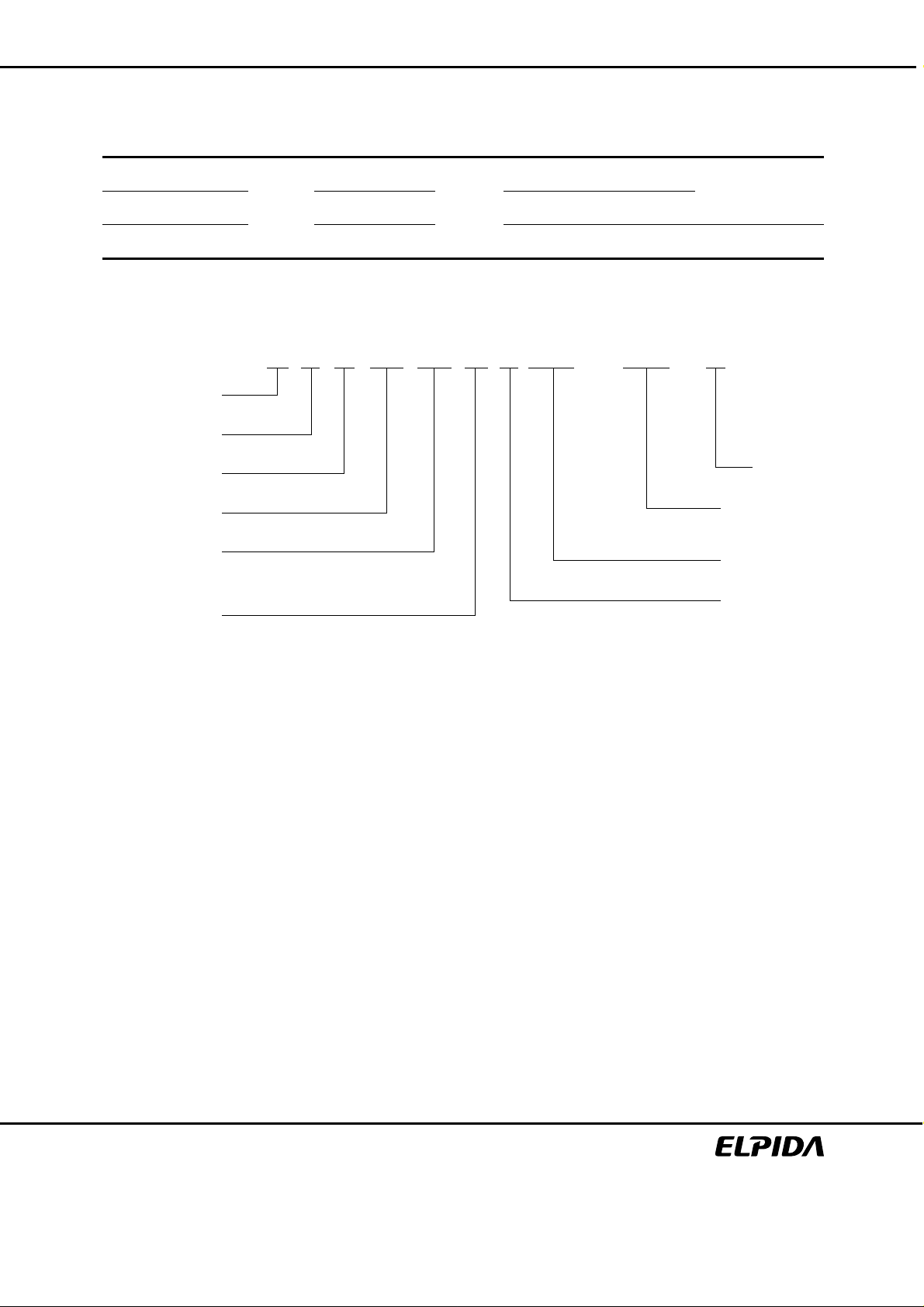
Ordering Information
Part number
EDE5104GBSA-5A-E
EDE5104GBSA-4A-E
EDE5108GBSA-5A-E
EDE5108GBSA-4A-E
EDE5116GBSA-5A-E
EDE5116GBSA-4A-E
Part Number
Elpida Memory
Type
D: Monolithic Device
Product Code
E: DDR-II
Density / Bank
51: 512M /4 banks
Bit Organization
04: x4
08: x8
16: x16
Voltage, Interface
G: 1.8V, SSTL_18
Mask
version
B 128M × 4 4
64M × 8
32M × 16
EDE5104GBSA, EDE5108GBSA, EDE5116GBSA
Organization
(words × bits)
Internal
Banks
Data rate
(Mbps)
533
400
533
400
533
400
/CAS latency Package
4, 5
3, 4, 5
4, 5
3, 4, 5
4, 5
3, 4, 5
64-ball µBGA
84-ball µBGA
E D E 51 04 G B SA - 4A - E
Lead Free
Speed
5A: 533Mbps
4A: 400Mbps
Package
SA: µBGA
Die Rev.
Preliminary Data Sheet E0249E 30 (Ver. 3.0)
2
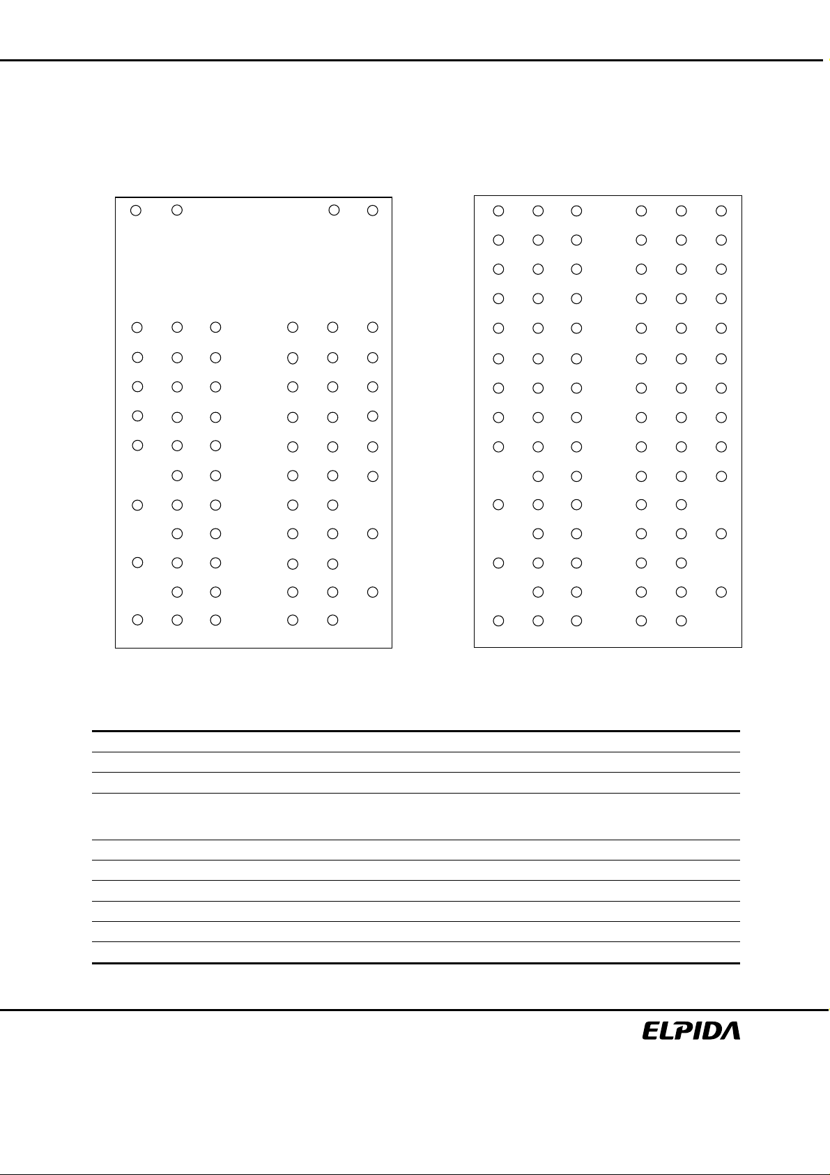
Pin Configurations
/xxx indicates active low signal.
EDE5104GBSA, EDE5108GBSA, EDE5116GBSA
64-ball µBGA
(×8, ×4 organization)
2
1
A
NC
B
C
D
E
F
G
H
J
K
L
M
N
P
R
VDD
DQ6
(NC)*
VDDQ
DQ4
(NC)*
VDDL
NC
VSS
VDD
NU/ /RDQS
(NC)*
VSSQ
DQ1
VSSQ
VREF
CKE
BA0
A10
A3
A7
A12
3
VSS
DM/RDQS
(DM)*
VDDQ
DQ3
VSS
/WE
BA1
A1
A5
A9
NC
7
VSSQ
DQS
VDDQ
DQ2
VSSDL
/RAS
/CAS
A2
A6
A11
NC
8
NCNC
/DQS
VSSQ
DQ0
VSSQ
CK
/CK
/CS
A0
A4
A8
A13
9
NC
VDDQ
DQ7
(NC)*
VDDQ
DQ5
(NC)*
VDD
ODT
VDD
VSS
1
A
VDD
B
C
VDDQ
D
E
VDD
F
DQ6
G
H
DQ4
J
VDDL
K
L
M
N
VSS
P
R
VDD
84-ball µBGA
(×16 organization)
2
3
VSSNC
VSSQ UDMDQ14
DQ9
VDDQ
VSSQDQ12
DQ11
NC
VSS
VSSQ
VSSQ
VREF
LDM
DQ1VDDQ
VDDQ
DQ3
VSS
CKE /WE
BA0
BA1 /CAS /CSNC
A10
A1
A3
A5
A7
A9
A12 NC NC NC
7
VSSQ
/UDQS
UDQS
VSSQ DQ15
VDDQ
DQ10
VSSQ DQ13
VSSQ
/LDQS
LDQS
VSSQ
VDDQ
DQ2 VSSQ DQ5
VSSDL CK VDD
/RAS
A2
A6
A11
8
9
VDDQ
DQ8
VDDQ
VDDQ
DQ7
DQ0 VDDQ
ODT
/CK
A0
VDD
A4
A8
VSS
(Top view)
Note: ( )* marked pins are for ×4 organization.
(Top view)
Pin name Function Pin name Function
A0 to A13 Address inputs ODT ODT control
BA0, BA1 Bank select VDD Supply voltage for internal circuit
DQ0 to DQ15 Data input/output VSS Ground for internal circuit
DQS, /DQS
UDQS, /UDQS
Differential data strobe VDDQ Supply voltage for DQ circuit
LDQS, /LDQS
RDQS, /RDQS Differential data strobe for read VSSQ Ground f or DQ circ uit
/CS Chip select VREF Reference supply voltage
/RAS, /CAS, / WE Command input VDDL Supply voltage for DLL circuit
CKE Clock enable VSSDL Ground for DLL circuit
CK, /CK Differential Clock i nput NC*1 No connection
DM, UDM, LDM Write Data mask NU*2 Not usable
Notes: 1. Not internally connected with die.
2. Don’t use other than reserved functions.
Preliminary Data Sheet E0249E 30 (Ver. 3.0)
3

CONTENTS
EDE5104GBSA, EDE5108GBSA, EDE5116GBSA
Description.....................................................................................................................................................1
Features.........................................................................................................................................................1
Ordering Information......................................................................................................................................2
Part Number ..................................................................................................................................................2
Pin Configurations .........................................................................................................................................3
Electrical Specific atio ns.................................................................................................................................5
Block Diagram .............................................................................................................................................10
Pin Function.................................................................................................................................................11
Command Operation ...................................................................................................................................13
Simplified State Diagram.............................................................................................................................20
Operation of DDR-II SDRAM.......................................................................................................................21
Package Drawing ........................................................................................................................................54
Recommended Soldering Conditions..........................................................................................................54
Preliminary Data Sheet E0249E 30 (Ver. 3.0)
4
EDE5104GBSA, EDE5108GBSA, EDE5116GBSA
Electrical Specifications
• All voltages are referenced to VSS (GND)
• Execute power-up and Initialization sequence before proper device operation is achieved.
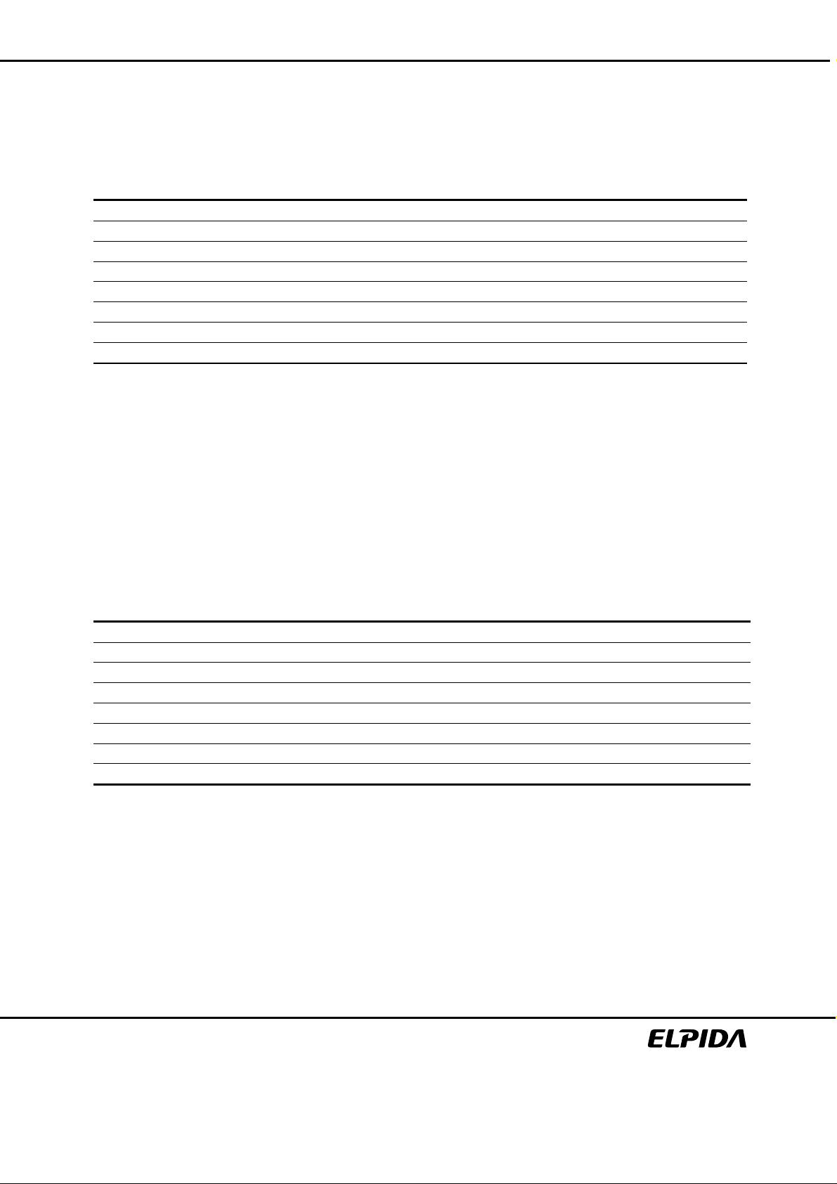
Absolute Maximum Ratings
Parameter Symbol Rating Unit Note
Power supply voltage VDD –0.5 to +2.3 V 1
Power supply voltage for output VDDQ –0.5 to +2.3 V 1
Input voltage VIN –0.5 to +2.3 V 1
Output voltage VOUT –0.5 to +2.3 V 1
Operating temperature (ambient) TA 0 t o +70 °C 1
Storage temperature TSTG –55 to +150 °C 1
Power dissipation PD 1.0 W 1
Short circuit output current IOUT 50 mA 1
Note: 1. Stresses greater than those listed under “Absolute Maximum Ratings” may cause permanent damage to
the device. This is a stress rating only and functional operation of the device at these or any other
conditions above those indicated in the operational sections of this specification is not implied. Exposure
to absolute maximum rating conditions for extended periods may affect reliability.
Caution
Exposing the device to stress above those listed in Absolute Maximum Ratings could cause
permanent damage. The device is not meant to be operated under conditions outside the limits
described in the operational section of this specification. Exposure to Absolute Maximum Rating
conditions for extended periods may affect device reliability.
Recommended DC Operating Conditions (SSTL_18)
• There is no specific device VDD supply voltage requirement for SSTL_18 compliance. However under all
conditions VDDQ must be less than or equal to VDD.
Parameter Symbol min. Typ. max. Unit Notes
Supply voltage VDD 1.7 1.8 1.9 V 4
Supply voltage for output VDDQ 1.7 1.8 1.9 V 4
Input reference voltage VREF 0.49 × VDDQ 0.50 × VDDQ 0.51 × VDDQ V 1, 2
Termination voltage VTT VREF – 0.04 VREF VREF + 0.04 V 3
DC input logic high VIH (dc) VREF + 0.125 VDDQ + 0.3V V
DC input low VIL (dc) –0.3 VREF – 0.125 V
AC input logic high VIH (ac) VREF + 0.250 V
AC input low VIL (ac) VREF – 0.250 V
Notes: 1. The value of VREF may be selected by the user to provide optimum noise margin in the system. Typically
the value of VREF is expected to be about 0.5 × VDDQ of the transmitting device and VREF are expected
to track variations in VDDQ.
2. Peak to peak AC noise on VREF may not exceed ±2% VREF (dc).
3. VTT of transmitting device must track VREF of receiving device.
4. VDDQ tracks with VDD, VDDL tracks with VDD. AC parameters are measured with VDD, VDDQ and
VDDL tied together.
Preliminary Data Sheet E0249E 30 (Ver. 3.0)
5

EDE5104GBSA, EDE5108GBSA, EDE5116GBSA
DC Characteristics 1 (TA = 0 to +70°°°°C, VDD, VDDQ = 1.8V ± 0.1V)
max.
Parameter Symbol Grade × 4, × 8 × 16 Unit Test condition
Operating current
(ACT-PRE)
Operating current
(ACT-READ-PRE)
Precharge power-down
standby current
Idle standby current IDD2N TBD TBD mA
Active power-down
standby current
Active standby current IDD3N TBD TBD m A
Operating current
(Burst read operating)
Operating current
(Burst write operating)
Auto-refresh current IDD5 TBD TBD mA tRC = tRFC (min.)
Self-refresh current IDD6 TBD TBD mA Self Refresh Mode; CKE = 0. 2V
Operating current
(Bank interleaving)
IDD0 TBD TBD mA
IDD1 TBD TBD mA
IDD2P TBD TBD mA
IDD3P TBD TBD mA
IDD4R TBD TBD mA
IDD4W TBD TBD mA
IDD7 TBD TBD mA
one bank; tRC = tRC (min.) ; t CK = tCK (min.) ; DQ,
DM, and DQS inputs changing twice per cl ock cycle;
address and control inputs c hangi ng once per clock
cycle
one bank; Burst = 4; tRC = tRC (min.) ;
CL = 4; tCK = tCK (min.) ; IOUT = 0mA;
address and control inputs c hangi ng once per clock
cycle
all banks idle; power-down mode; CKE = VIL (max.);
tCK = tCK (min.)
/CS = VIH (min.); all banks idle; CKE = VIH (min.);
tCK = tCK (min.) ; address and control inputs
changing once per clock cyc l e
one bank active; power-down mode; CKE = VIL
(max.);
tCK = tCK (min.)
one bank; active;/CS = V IH (min.);
CKE = VIH (min.); tRC = tRAS max; tCK = tCK
(min.); DQ, DM, and DQS input s changing twice per
clock cycle; addres s and control inputs changing
once per clock cycle
one bank; Burst = 4; burst; address and control
inputs changing once per cloc k cycle; DQ and DQS
outputs changing twice per cloc k cycle; CL = 4; tCK
= tCK (min.) ; IOUT = 0mA
one bank; Burst = 4; writes; continuous burst;
address and control inputs c hangi ng once per clock
cycle; DQ and DQS inputs changi ng twice per clock
cycle; CL = 4;
tCK = tCK (min.)
Four bank interleaving READs (BL4) with aut o
precharge, tRC = tRC (min.); Address and control
inputs change during Active, READ, or WRITE
commands.
DC Characteristics 2 (TA = 0 to +70°°°°C, VDD, VDDQ = 1.8V ± 0.1V)
Parameter Symbol Unit Notes
Minimum required output pull -up under A C
test load
Maximum required output pull-down under
AC test load
Output timing m easurement reference level VOTR 0.5 × VDDQ V 1
Output minimum sink DC current IOL +13.4 mA 3, 4, 5
Output minimum source DC current IOH –13.4 mA 2, 4, 5
VOH VTT + 0.603 V 5
VOL VTT – 0.603 V 5
Note: 1. The VDDQ of the device under test is referenced.
2. VDDQ = 1.7V; VOUT = 1.42V.
3. VDDQ = 1.7V; VOUT = 0.28V.
4. The DC value of VREF applied to the receiving device is expected to be set to VTT.
5. After OCD calibration to 18Ω at TA = 25°C, VDD = VDDQ = 1.8V.
Preliminary Data Sheet E0249E 30 (Ver. 3.0)
6
EDE5104GBSA, EDE5108GBSA, EDE5116GBSA
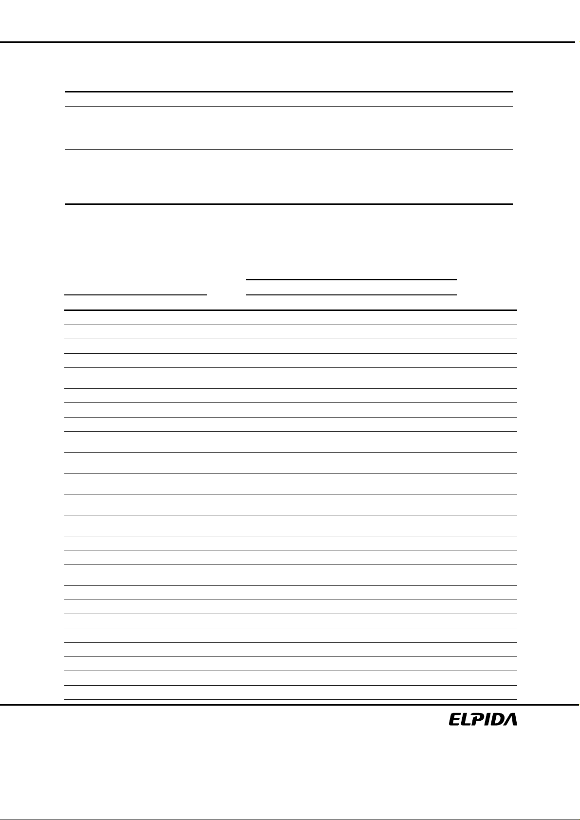
Pin Capacitance (TA = 25°C, VDD, VDDQ = 1.8V ± 0.1V)
Parameter Symbol Pins min. Typ max. Unit
CLK input pin capacitance CCK CK 1.5 2.0 2.5 pF 1
/RAS, /CAS,
Input pin capacitance CIN
Input/output pin capaci t ance CI/O
/WE, /CS,
CKE. ODT,
Address
DQ, DQS, /DQS,
UDQS, /UDQS,
LDQS, /LDQS,
/RDQS, /RDQS,
DM, UDM, LDM
1.5 2.0 2.5 pF 1
3.0 3.5 4.0 pF 2
Notes: 1. Matching within 0.25pF.
2. Matching within 0.50pF.
AC Characteristics (TA = 0 to +70°°°°C, VDD, VDDQ = 1.8V ± 0.1V, VSS, VSSQ = 0V)
-5A -4A
Frequency (Mbps) 533 400
Parameter Symbol min. max. min. max. Unit Notes
DQ output access time from CK, /CK tAC –500 +500 –600 +600 ps
DQS output access ti me from CK, /CK tDQSCK –450 +450 –500 +500 ps
CK high-level width tCH 0.45 0.55 0.45 0.55 tCK
CK low-level width tCL 0.45 0.55 0.45 0.55 tCK
CK half period tHP
Clock cycle time tCK 3750 8000 5000 8000 ps
DQ and DM input hold time tDH 350 400 ps
DQ and DM input setup time tDS 350 400 ps
Control and Address input pulse width
for each input
DQ and DM input pulse width for each
input
Data-out high-impedance time from
CK,/CK
Data-out low-impedance tim e from
CK,/CK
DQS-DQ skew for DQS and associated
DQ signals
DQ hold skew factor tQHS 400 450 ps
DQ/DQS output hold time f rom DQS tQH tHP – tQHS tHP – tQHS ps
Write command to first DQS l atching
transition
DQS input high pulse width tDQSH 0.35 0.35 tCK
DQS input low pulse width tDQSL 0.35 0.35 tCK
DQS falling edge to CK setup t i me t DS S 0.2 0.2 tCK
DQS falling edge hold time f rom CK tDSH 0.2 0.2 tCK
Mode register set command cycle time tMRD 2 2 tCK
Write preambl e setup time tWPRES 0 0 tCK
Write postamble tWPST 0.4 0.6 0.4 0.6 tCK
Write preambl e tWPRE 0.25 0.25 tCK
tIPW 0.6 0.6 tCK
tDIPW 0.35 0.35 tCK
tHZ tAC max. tAC max. ps
tLZ tAC min. tAC max. tAC min. tAC max. ps
tDQSQ 300 350 ps
tDQSS WL – 0.25 WL + 0. 25 WL – 0.25 WL + 0.25 tCK
min.
(tCL, tCH)
min.
(tCL, tCH)
ps
Notes
Preliminary Data Sheet E0249E 30 (Ver. 3.0)
7

EDE5104GBSA, EDE5108GBSA, EDE5116GBSA
-5A -4A
Frequency (Mbps) 533 400
Parameter Symbol min. max. min. max. Unit Notes
Address and control input hold time tIH 500 600 ps
ddress and A control input s etup time tIS 500 600 ps
Read preamble tRPRE 0.9 1.1 0.9 1.1 tCK
Read postamble tRPST 0.4 0.6 0.4 0.6 tCK
Active to precharge command tRAS 45 45 ns
Active to active/ auto refresh comm and
time
Active to read or write command delay tRCD 15 20 ns
Precharge command period tRP 15 20 ns
Active to auto-precharge delay tRAP tRCD mi n. tRCD min. ns
Active bank A to active bank B
command period
(EDE5104GB, EDE5108GB)
(EDE5116GB) tRRD 10 10 ns
Write recovery t i me tWR 15 15 ns
Auto precharge write recovery +
precharge time
Internal write to read comm and del ay tWTR 7.5 10 ns
Exit self refresh to any command tXSC 200 200 tCK
Exit power down to any non-read
command
Exit precharge power down to read
command
Exit active power down to read
command
Exit active power down to read
command
(slow exit/low power mode)
Output impedance test driver delay tOIT 0 12 0 12 ns
Auto refresh to active/ auto refresh
command time
Average periodic refresh interval tREFI 7.8 7.8 µs
Notes: 1. For each of the terms above, if not already an integer, round to the next highest integer.
2. AL: Additive Latency.
3. MRS A12 bit define which active power down exit timing to be applied.
tRC 60 65 ns
tRRD 7.5 10 ns
tDAL
tXPNR 2 2 tCK
tXPRD 6 – AL 6 – AL tCK 2
tXARD 2 2 tCK 3
tXARDS 6 – AL 6 – AL tCK 3
tRFC 105 105 ns
(tWR/tCK)+
(tRP/tCK)
(tWR/tCK)+
(tRP/tCK)
tCK 1
Preliminary Data Sheet E0249E 30 (Ver. 3.0)
8
EDE5104GBSA, EDE5108GBSA, EDE5116GBSA
AC Electrical Characteristics and Operating Conditions
Parameter Symbol min max Unit Notes
ODT turn-on delay tAOND 2 2 tCK
ODT turn-on tAON tAC(min) tAC(max) + 1000 ps 1
ODT turn-on (power - down mode) tAONPD tAC(min) + 2000 2tCK + tAC(max) + 1000 ps
ODT turn-off delay tAOFD 2.5 2.5 tCK
ODT turn-off tAOF tAC(min) tAC(max) + 600 ps 2
ODT turn-off (power - down mode) tAOFPD tAC(min) + 2000 2.5tCK + tAC(max) + 1000 ns
Notes: 1. ODT turn on time min is when the device leaves high impedance and ODT resistance begins to turn on.
ODT turn on time max is when the ODT resistance is fully on. Both are measured from tAOND.
2. ODT turn off time min is when the device starts to turn off ODT resistance.
ODT turn off time max is when the bus is in high impedance. Both are measured from tAOFD.
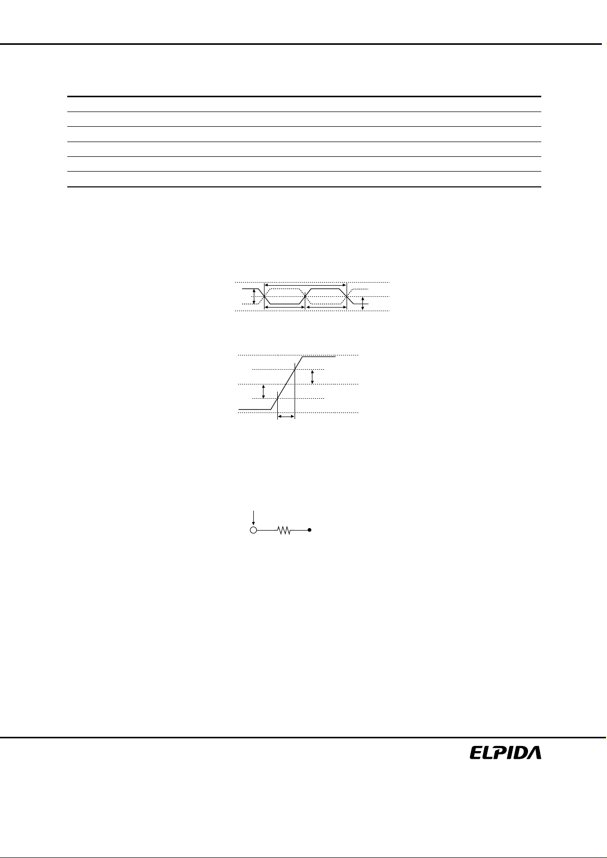
Test Conditions
CLK
VSWING
/CLK
VIL
Measurement point
DQ
tCK
VX
tCL
∆t
SLEW = (VIH (ac) – VIL (ac))/∆t
RT =25 Ω
tCH
VIH
VTT
VDD
VREF
VSS
VDD
VREF
VSS
Preliminary Data Sheet E0249E 30 (Ver. 3.0)
9
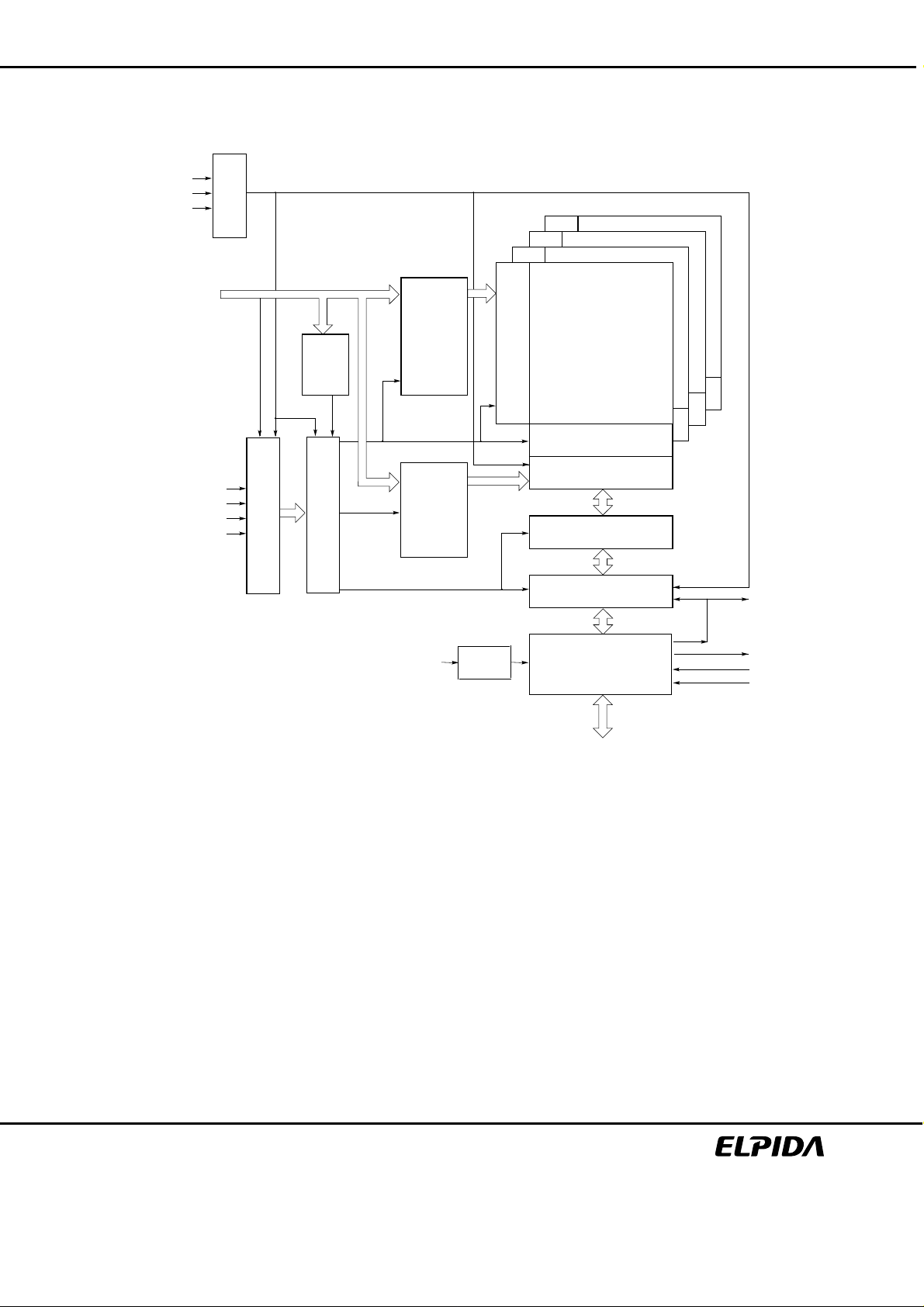
Block Diagram
CK
/CK
CKE
Clock
generator
EDE5104GBSA, EDE5108GBSA, EDE5116GBSA
Bank 3
Bank 2
Bank 1
A0 to A13, BA0, BA1
/RAS
/CAS
/CS
/WE
Mode
register
Control logic
Command decoder
Row
address
buffer
and
refresh
counter
Column
address
buffer
and
burst
counter
DLLCK, /CK
Memory cell array
Row decoder
Sense amp.
Column decoder
Data control circuit
Latch circuit
Input & Output buffer
Bank 0
DQS, /DQS
RDQS, /RDQS
ODT
DM
DQ
Preliminary Data Sheet E0249E 30 (Ver. 3.0)
10
EDE5104GBSA, EDE5108GBSA, EDE5116GBSA
Pin Function
CK, /CK (input pins)
CK and /CK are differential clock inputs. All address and control input signals are sampled on the crossing of the
positive edge of CK and negative edge of /CK. Output (read) data is referenced to the crossings of CK and /CK
(both directions of crossing).
/CS (input pin)
All commands are masked when /CS is registered High. /CS provides for external bank selection on systems with
multiple banks. /CS is considered part of the command code.
/RAS, /CAS, /WE (input pins)
/RAS, /CAS and /WE (along with /CS) define the command being entered.
A0 to A13 (input pins)
Provided the row address for Active commands and the column address and Auto Precharge bit for Read/Write
commands to select one location out of the memory array in the respective bank.
[Address Pins Table]
Address (A0 to A13)
Part number Row address Column address
EDE5104GB AX0 to AX13 AY0 to AY9, AY11
EDE5108GB AX0 to AX13 AY0 to AY9
EDE5116GB AX0 to AX12 AY0 to AY9
Notes: 1. A13 pin is NC for ×16 organization.
A10 (AP) (input pin)
A10 is sampled during a precharge command to determine whether the precharge applies to one bank (A10 = Low)
or all banks (A10 = High). If only one bank is to be precharged, the bank is selected by BA0, BA1. The address
inputs also provide the op-code during mode register set commands.
BA0, BA1 (input pins)
BA0 and BA1 define to which bank an active, read, write or precharge command is being applied. BA0 also
determines if the mode register or extended mode register is to be accessed during a MRS or EMRS cycle.
[Bank Select Signal Table]
BA0 BA1
Bank 0 L L
Bank 1 H L
Bank 2 L H
Bank 3 H H
Remark: H: VIH. L: VIL.
CKE (input pin)
CKE High activates, and CKE Low deactivates, internal clock signals and device input buffers and output drivers.
Taking CKE Low provides precharge power-down and Self Refresh operation (all banks idle), or active power-down
(row active in any bank). CKE is synchronous for power down entry and exit, and for self refresh entry. CKE is
asynchronous for self refresh exit. CKE must be maintained high throughout read and write accesses. Input buffers,
excluding CK, /CK and CKE are disabled during power-down. Input buffers, excluding CKE, are disabled during self
refresh.
Notes
1
Preliminary Data Sheet E0249E 30 (Ver. 3.0)
11

EDE5104GBSA, EDE5108GBSA, EDE5116GBSA
DM, UDM and LDM (input pins)
DM is an input mask signal for write data. In 32M × 16 products, UDM and LDM control upper byte (DQ8 to DQ15)
and lower byte (DQ0 to DQ7). Input data is masked when DM is sampled High coincident with that input data during
a Write access. DM is sampled on both edges of DQS. Although DM pins are input only, the DM loading matches
the DQ and DQS loading. For ×8 configuration, DM function will be disabled when RDQS function is enabled by
EMRS.
DQ (input/output pins)
Bi-directional data bus.
DQS, /DQS, UDQS, /UDQS, LDQS, /LDQS (input/output pins)
Output with read data, input with write data for source synchronous operation. In 32M × 16 products, UDQS, /UDQS
and LDQS, /LDQS control upper byte (DQ8 to DQ15) and lower byte (DQ0 to DQ7). Edge-aligned with read data,
centered in write data. Used to capture write data. /DQS can be disabled by EMRS.
RDQS, /RDQS (output pins)
Differential Data Strobe for READ operation only. DM and RDQS functions are switch able by EMRS. These pins
exist only in ×8 configuration. /RDQS output will be disabled when /DQS is disabled by EMRS.
ODT (input pins)
ODT (On Die Termination control) is a registered High signal that enables termination re sistanc e internal to the DDR
II SDRAM. When enabled, ODT is only applied to each DQ, DQS, /DQS, RDQS, /RDQS, and DM signal for × 4, × 8
configurations. For × 16 configuration, ODT is applied to each DQ, UDQS, /UDQS, LDQS, /LDQS, UDM, and LDM
signal. The ODT pin will be ignored if the Extended Mode Register (EMRS) is programmed to disable ODT.
VDD, VSS, VDDQ, VSSQ (power supply)
VDD and VSS are power supply pins for internal circuits. VDDQ and VSSQ are power supply pins for the output
buffers.
VDDL and VSSDL (power supply)
VDDL and VSSDL are power supply pins for DLL circuits.
VREF (Power supply)
SSTL_18 reference voltage: (0.50 ± 0.01) × VDDQ
Preliminary Data Sheet E0249E 30 (Ver. 3.0)
12

EDE5104GBSA, EDE5108GBSA, EDE5116GBSA
Command Operation
Command Truth Table
The DDR-II SDRAM recognizes the following commands specified by the /CS, /RAS, /CAS, /WE and address pins.
CKE
Function
Mode register set MRS H H L L L L BA0 = 0 and MRS OP Code 1
Extended mode register set EMRS H H L L L L BA0 = 1 and EMRS OP Code 1
Auto (CBR) refresh REF H H L L L H × × × × 1
Self refresh entry SELF H L L L L H × × × × 1
Self refresh exit SELFX L H H × × × × × × × 1
Single bank precharge PRE H H L L H L BA × L × 1, 2
Precharge all banks PALL H H L L H L × × H × 1
Bank activate ACT H H L L H H BA Row Address 1, 2
Write WRIT H H L H L L BA Column L Column 1, 2, 3
Write with auto precharge WRITA H H L H L L BA Column H Column 1, 2, 3
Read READ H H L H L H BA Column L Column 1, 2, 3
Read with auto precharge READA H H L H L H BA Column H Column 1, 2, 3
No operation NOP H × L H H H × × × × 1
Device deselect DESL H × H × × × × × × × 1
Power down mode entry PDEN H L × × × × × × × × 1, 4, 5
Power down mode exit P DE X L H × × × × × × × × 1, 4, 5
Symbol
Previous
cycle
Current
cycle /CS /RAS /CAS /WE
BA1,
BA0
Remark: H = VIH. L = VIL. × = VIH or VIL
Notes: 1. All DDR-II commands are defined by states of /CS, /RAS, /CAS, /WE, and CKE at the rising edge of the
clock.
2. Bank Select (BA0, BA1), determine which bank is to be operated upon.
3. Burst reads or writes should not be terminated other than specified as ″Reads interrupted by a Read″ in
Burst Read command [READ] or ″Writes interrupted by a Write″ in Burst Write command [WRIT].
4. The Power Down Mode does not perform any refresh operations. The duration of Power Down is
therefore limited by the refresh requirements of the device. One clock delay is required for mode entry and
exit.
5. The state of ODT does not affect the states described in this table. The ODT function is not available
during Self Refresh.
A13 to
A11 A10
A0 to
A9
Notes
Preliminary Data Sheet E0249E 30 (Ver. 3.0)
13
EDE5104GBSA, EDE5108GBSA, EDE5116GBSA
CKE Truth Table
CKE Command
Current state Function
Self refresh INVALID H × × × × × × 1
Illegal L H L Command Address 2
Maintain self refresh L L × × × × ×
Power down INVA LID H × × × × × × 1
Power down mode exit L H H × × × × 2
ILLEGAL L H L
Maintain power down mode L L × × × × ×
All banks idle Device deselect H H H × × × 3
Power down H L H × × ×
Entry self refresh H L L L L H × 4
Any state other
than listed
above
ILLEGAL L × × × × × ×
Exit self refresh with device
deselect
Exit self refresh with no
operation
Refer to the current state truth
table
Register command begin power
down next cycle
Refer to operations in the
current state truth tabl e
Power down entry H L × × × × × 5
Previous
Cycle
L H H × × × × 2
L H L H H H × 2
H H L Command Address 3
H L L Command Address 3
H H × × × × ×
Remark: H = VIH. L = VIL. × = VIH or VIL
Notes: 1. For the given Current State CKE must be low in the previous cycle.
2. W hen CKE has a low to high transitio n, the clock and o ther inputs are r e-enabled asyn chronously. The
minimum setup time for CKE (tCES) must be satisfied before any command other than self refresh exit.
3. The inputs (BA1, BA0, A13 to A0) depend on the command that is issued. See the Command Truth Table
for more information.
4. The Auto Refresh, Self Refresh mode, and the Mode Register Set modes can only be entered from the all
banks idle state.
5. Must be a legal command as defined in the Command Truth Table.
Current
Cycle
/CS /RAS /CAS /WE
Command
except NOP
BA1,BA0,
A13 to A0 Notes
Address 2
Preliminary Data Sheet E0249E 30 (Ver. 3.0)
14
EDE5104GBSA, EDE5108GBSA, EDE5116GBSA
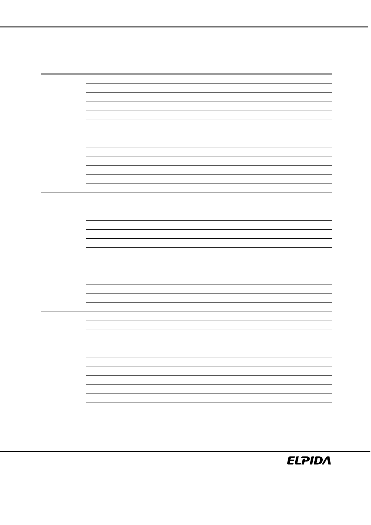
Function Truth Table
The following tables show the operations that are performed when each command is issued in each state of the
DDR SDRAM.
Current state /CS /RAS /CAS /WE Address Command Operation Notes
Idle H × × × × DESL Nop or Power down
L H H H × NOP Nop or Power down
L H L H
L H L H
L H L L
L H L L
L L H H
L L H L
L L H L
L L L H × REF Auto refresh 2
L L L H × SELF Self refresh 2
L L L L
L L L L
Bank(s) active H × × × × DESL Nop
L H H H × NOP Nop
L H L H
L H L H
L H L L
L H L L
L L H H
L L H L
L L H L
L L L H × REF ILLEGAL
L L L H × SELF ILLEGAL
L L L L
L L L L
Read H × × × × DESL Continue burst to end -> Row active
L H H H × NOP Continue burst to end -> Row acti ve
L H L H
L H L H
L H L L
L H L L
L L H H
L L H L
L L H L
L L L H × REF ILLEGAL
L L L H × SELF ILLEGAL
L L L L
L L L L
BA, CA, A10 (AP)
BA, CA, A10 (AP)
BA, CA, A10 (AP)
BA, CA, A10 (AP)
BA, RA
BA, A10 (AP)
A10 (AP)
BA, MRS-OPCODE
BA, EMRS-OPCODE
BA, CA, A10 (AP)
BA, CA, A10 (AP)
BA, CA, A10 (AP)
BA, CA, A10 (AP)
BA, RA
ACT ILLEGAL 1
BA, A10 (AP)
A10 (AP)
BA, MRS-OPCODE
BA, EMRS-OPCODE
BA, CA, A10 (AP)
BA, CA, A10 (AP)
BA, CA, A10 (AP)
BA, CA, A10 (AP)
BA, RA
BA, A10 (AP)
A10 (AP)
BA, MRS-OPCODE
BA, EMRS-OPCODE
PRE Precharge
PALL Precharge all banks
ACT ILLEGAL 1
PRE ILLEGAL 1
PALL ILLEGAL
READ ILLEGAL 1
READA ILLEGAL 1
WRIT ILLEGAL 1
WRITA ILLEGAL 1
ACT Row activating
PRE Precharge
PALL Precharge all banks
MRS Mode register accessing 2
EMRS Extended m ode regi ster accessing 2
READ Begin Read
READA Begin Read
WRIT Begin Write
WRITA Begin Write
MRS ILLEGAL
EMRS ILLEGAL
READ Burst interrupt 1, 4
READA Burst interrupt 1, 4
WRIT ILLEGAL 1
WRITA ILLEGAL 1
MRS ILLEGAL
EMRS ILLEGAL
Preliminary Data Sheet E0249E 30 (Ver. 3.0)
15
EDE5104GBSA, EDE5108GBSA, EDE5116GBSA
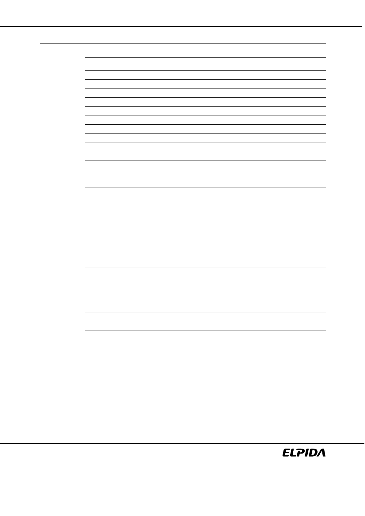
Current state /CS /RAS /CAS /WE Address Command Operation Note
Write H × × × × DESL
L H H H × NOP
L H L H
L H L H
L H L L
L H L L
L L H H
L L H L
L L H L
BA, CA, A10 (AP)
BA, CA, A10 (AP)
BA, CA, A10 (AP)
BA, CA, A10 (AP)
BA, RA
ACT ILLEGAL 1
BA, A10 (AP)
A10 (AP)
READ ILLEGAL 1
READA ILLEGAL 1
WRIT Burst interrupt 1, 4
WRITA Burst interrupt 1, 4
PRE ILLEGAL 1
PALL ILLEGAL
L L L H × REF ILLEGAL
L L L H × SELF ILLEGAL
L L L L
L L L L
BA, MRS-OPCODE
BA, EMRS-OPCODE
MRS ILLEGAL
EMRS ILLEGAL
Read with H × × × × DESL Continue burst to end -> Precharging
auto precharge L H H H × NOP Continue burst to end -> Precharging
L H L H
L H L H
L H L L
L H L L
L L H H
L L H L
L L H L
BA, CA, A10 (AP)
BA, CA, A10 (AP)
BA, CA, A10 (AP)
BA, CA, A10 (AP)
BA, RA
ACT ILLEGAL 1
BA, A10 (AP)
A10 (AP)
READ ILLEGAL 1
READA ILLEGAL 1
WRIT ILLEGAL 1
WRITA ILLEGAL 1
PRE ILLEGAL 1
PALL ILLEGAL
L L L H × REF ILLEGAL
L L L H × SELF ILLEGAL
L L L L
L L L L
Write with auto
Precharge
H × × × × DESL
BA, MRS-OPCODE
BA, EMRS-OPCODE
MRS ILLEGAL
EMRS ILLEGAL
L H H H × NOP
L H L H
L H L H
L H L L
L H L L
L L H H
L L H L
L L H L
BA, CA, A10 (AP)
BA, CA, A10 (AP)
BA, CA, A10 (AP)
BA, CA, A10 (AP)
BA, RA
ACT ILLEGAL 1
BA, A10 (AP)
A10 (AP)
READ ILLEGAL 1
READA ILLEGAL 1
WRIT ILLEGAL 1
WRITA ILLEGAL 1
PRE ILLEGAL 1
PALL ILLEGAL
L L L H × REF ILLEGAL
L L L H × SELF ILLEGAL
L L L L
L L L L
BA, MRS-OPCODE
BA, EMRS-OPCODE
MRS ILLEGAL
EMRS ILLEGAL
Continue burst to end
-> Write recovering
Continue burst to end
-> Write recovering
Continue burst to end
->Write recovering with aut o precharge
Continue burst to end
->Write recovering with aut o precharge
Preliminary Data Sheet E0249E 30 (Ver. 3.0)
16
EDE5104GBSA, EDE5108GBSA, EDE5116GBSA
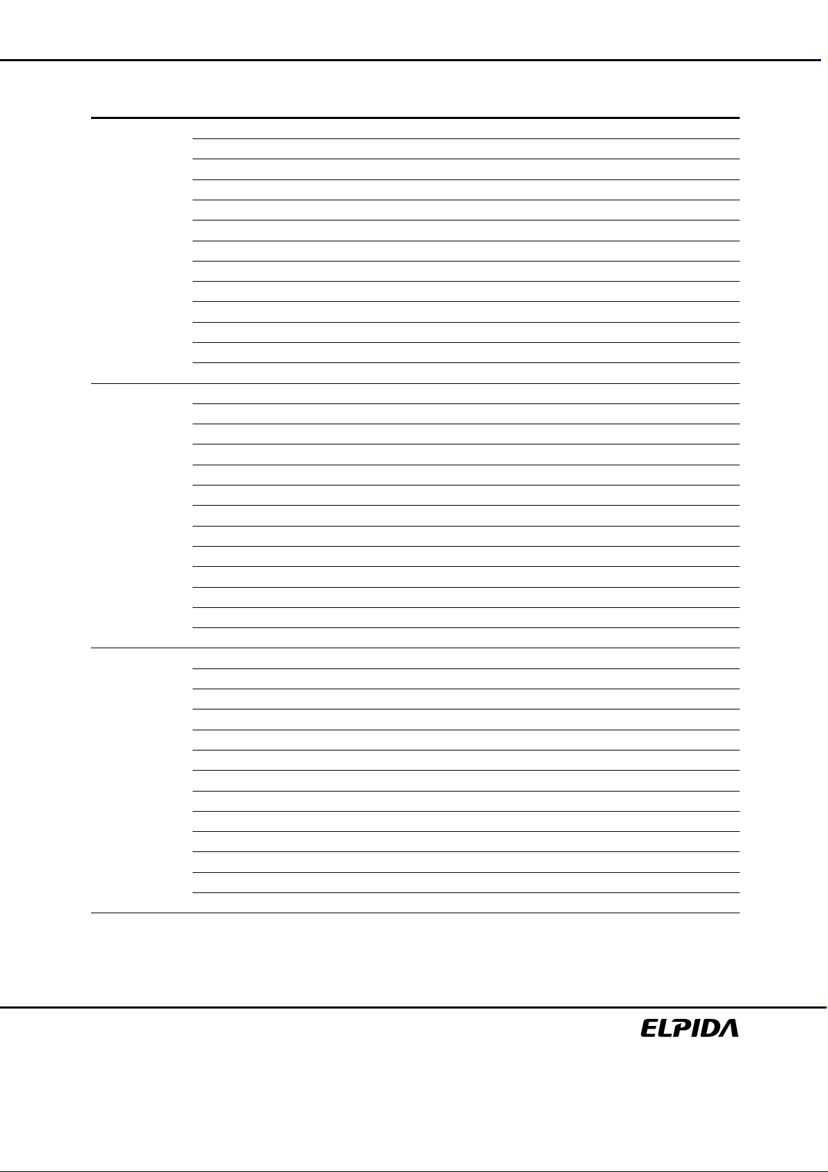
Current state /CS /RAS /CAS /WE Address Command Operation Note
Precharging H × × × × DESL Nop -> Enter idle after tRP
L H H H × NOP Nop -> Enter idle after tRP
L H L H
L H L H
L H L L
L H L L
L L H H
L L H L
L L H L
L L L H × REF ILLEGAL
L L L H × SELF ILLEGAL
L L L L
L L L L
Row activating H × × × × DESL Nop -> Enter bank active after tRCD
L H H H × NOP Nop -> Enter bank active after tRCD
L H L H
L H L H
L H L L
L H L L
L L H H
L L H L
L L H L
L L L H × REF ILLEGAL
L L L H × SELF ILLEGAL
L L L L
L L L L
Write recovering H × × × × DES L Nop -> Enter bank active after tWR
L H H H × NOP Nop -> Enter bank ac tive after tWR
L H L H
L H L H
L H L L
L H L L
L L H H
L L H L
L L H L
L L L H × REF ILLEGAL
L L L H × SELF ILLEGAL
L L L L
L L L L
BA, CA, A10 (AP)
BA, CA, A10 (AP)
BA, CA, A10 (AP)
BA, CA, A10 (AP)
BA, RA
ACT ILLEGAL 1
BA, A10 (AP)
A10 (AP)
BA, MRS-OPCODE
BA, EMRS-OPCODE
BA, CA, A10 (AP)
BA, CA, A10 (AP)
BA, CA, A10 (AP)
BA, CA, A10 (AP)
BA, RA
ACT ILLEGAL 1
BA, A10 (AP)
A10 (AP)
BA, MRS-OPCODE
BA, EMRS-OPCODE
BA, CA, A10 (AP)
BA, CA, A10 (AP)
BA, CA, A10 (AP)
BA, CA, A10 (AP)
BA, RA
ACT ILLEGAL 1
BA, A10 (AP)
A10 (AP)
BA, MRS-OPCODE
BA, EMRS-OPCODE
READ ILLEGAL 1
READA ILLEGAL 1
WRIT ILLEGAL 1
WRITA ILLEGAL 1
PRE Nop -> Enter idle after tRP
PA LL Nop -> Enter idl e after tRP
MRS ILLEGAL
EMRS ILLEGAL
READ ILLEGAL 1
READA ILLEGAL 1
WRIT ILLEGAL 1
WRITA ILLEGAL 1
PRE ILLEGAL
PALL ILLEGAL
MRS ILLEGAL
EMRS ILLEGAL
READ ILLEGAL 1
READA ILLEGAL 1
WRIT New write
WRITA New write
PRE ILLEGAL 1
PALL ILLEGAL
MRS ILLEGAL
EMRS ILLEGAL
Preliminary Data Sheet E0249E 30 (Ver. 3.0)
17
 Loading...