ELPID EDD5108ABTA-7B, EDD5108ABTA-7A, EDD5108ABTA-6B, EDD5104ABTA-7B, EDD5104ABTA-7A Datasheet
...
PRELIMINARY DATA SHEET
512M bits DDR SDRAM
EDD5104ABTA (128M words ×××× 4 bits)
EDD5108ABTA (64M words ×××× 8 bits)
Description
The EDD5104AB is a 512M bits Double Data Rate
(DDR) SDRAM organized as 33,554,432 words × 4 bits
× 4 banks. The EDD5108AB is a 512M bits DDR
SDRAM organized as 16,777,216 words × 8 bits × 4
banks. Read and write operations are performed at the
cross points of the CK and the /CK. This high-speed
data transfer is realized by the 2 bits prefetch-pipelined
architecture. Data strobe (DQS) both for read and
write are available for high speed and reliable data bus
design. By setting extended mode resistor, the on-chip
Delay Locked Loop (DLL) can be set enable or disable.
They are packaged in standard 66-pin plastic TSOP
(II)10.16mm(400).
Features
• 2.5 V power supply: VDDQ = 2.5V ± 0.2V
: VDD = 2.5V ± 0.2V
• Data Rate: 333Mbps/266Mbps (max.)
• Double Data Rate architecture; two data transfers per
clock cycle
• Bi-directional, data strobe (DQS) is transmitted
/received with data, to be used in capturing data at
the receiver
• Data inputs, outputs, and DM are synchronized with
DQS
• 4 internal banks for concurrent operation
• DQS is edge aligned with data for READs; center
aligned with data for WRITEs
• Differential clock inputs (CK and /CK)
• DLL aligns DQ and DQS transitions with CK
transitions
• Commands entered on each positive CK edge; data
and data mask referenced to both edges of DQS
• Data mask (DM) for write data
• Auto precharge option for each burst access
• 2.5 V (SSTL_2 compatible) I/O
• Programmable burst length (BL): 2, 4, 8
• Programmable /CAS latency (CL): 2, 2.5
• Refresh cycles: 8192 refresh cycles/64ms
7.8µs maximum average periodic refresh interval
• 2 variations of refresh
Auto refresh
Self refresh
Document No. E0237E30 (Ver. 3.0)
Date Published August 2002 (K) Japan
URL: http://www.elpida.com
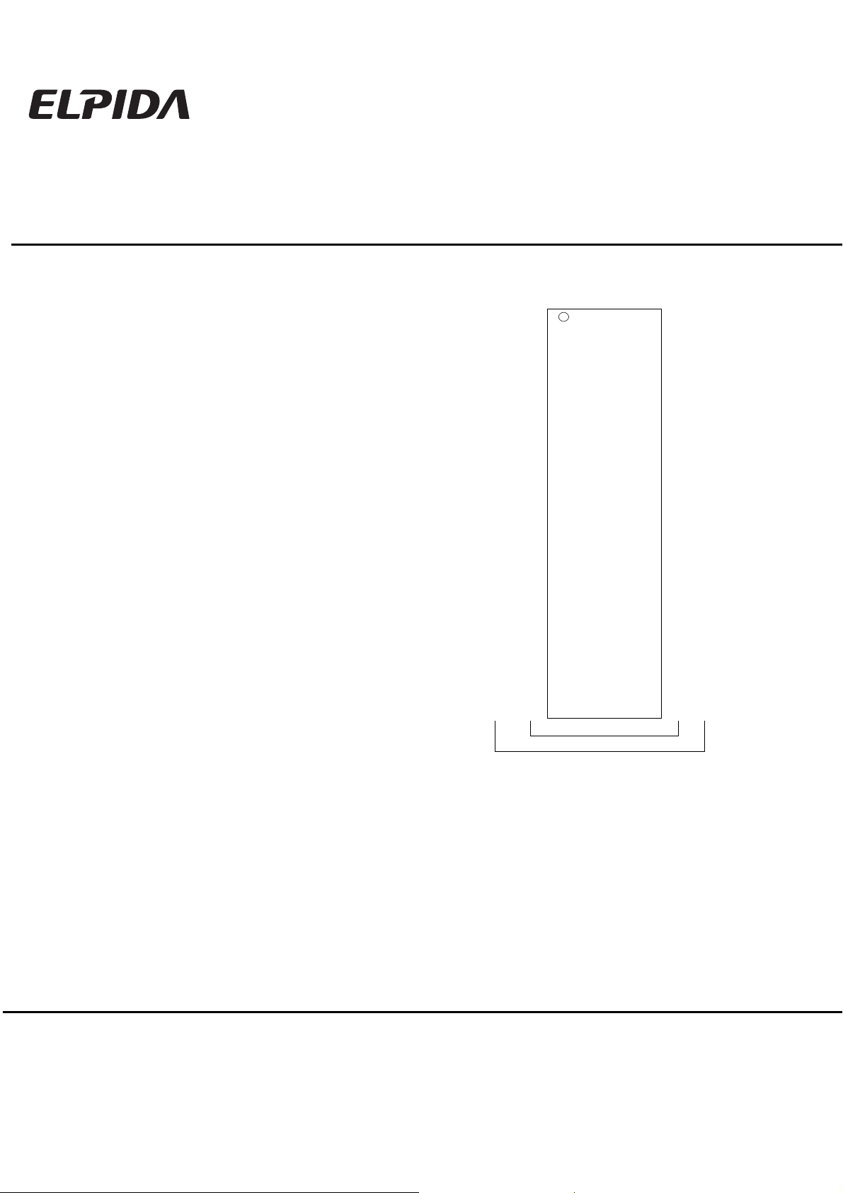
Pin Configurations
/xxx indicates active low signal.
66-pin TSOP(II)10.16mm(400)
VDD
VDD
DQ0
VDDQ
NC
DQ1
VSSQ
NC
DQ2
VDDQ
NC
DQ3
VSSQ
NC
NC
VDDQ
NC
NC
VDD
NC
NC
/WE
/CAS
/RAS
/CS
NC
BA0
BA1
VDD
1
2
3
4
5
6
7
8
9
10
11
12
13
14
15
16
17
18
19
20
21
22
23
24
25
26
27
28
A0
29
A1
30
A2
31
A3
32
33
X 8
X 4
(Top view)
Address input
Bank select address
Data-input/output
Input and output data strobe
Chip select
Row address strobe command
Column address strobe command
Write enable
Input mask
Clock input
Differential clock input
Clock enable
Input reference voltage
Power for internal circuit
Ground for internal circuit
Power for DQ circuit
Ground for DQ circuit
No connection
NC
VDDQ
NC
DQ0
VSSQ
NC
NC
VDDQ
NC
DQ1
VSSQ
NC
NC
VDDQ
NC
NC
VDD
NC
NC
/WE
/CAS
/RAS
/CS
NC
BA0
BA1
A10(AP)
A0
A1
A2
A3
VDD
A0 to A12
BA0, BA1
DQ0 to DQ7
DQS
/CS
/RAS
/CAS
/WE
DM
CK
/CK
CKE
VREF
VDD
VSS
VDDQ
VSSQ
NC
A10(AP)
66
65
64
63
62
61
60
59
58
57
56
55
54
53
52
51
50
49
48
47
46
45
44
43
42
41
40
39
38
37
36
35
34
DQ7
VSSQ
NC
DQ6
VDDQ
NC
DQ5
VSSQ
NC
DQ4
VDDQ
NC
NC
VSSQ
DQS
NC
VREF
VSS
DM
/CK
CK
CKE
NC
A12
A11
A9
A8
A7
A6
A5
A4
VSS
NC
VSSQ
NC
DQ3
VDDQ
NC
NC
VSSQ
NC
DQ2
VDDQ
NC
NC
VSSQ
DQS
NC
VREF
VSS
DM
/CK
CK
CKE
NC
A12
A11
A9
A8
A7
A6
A5
A4
VSS
VSS
VSS
Elpida Memory, Inc. 2002
Ordering Information
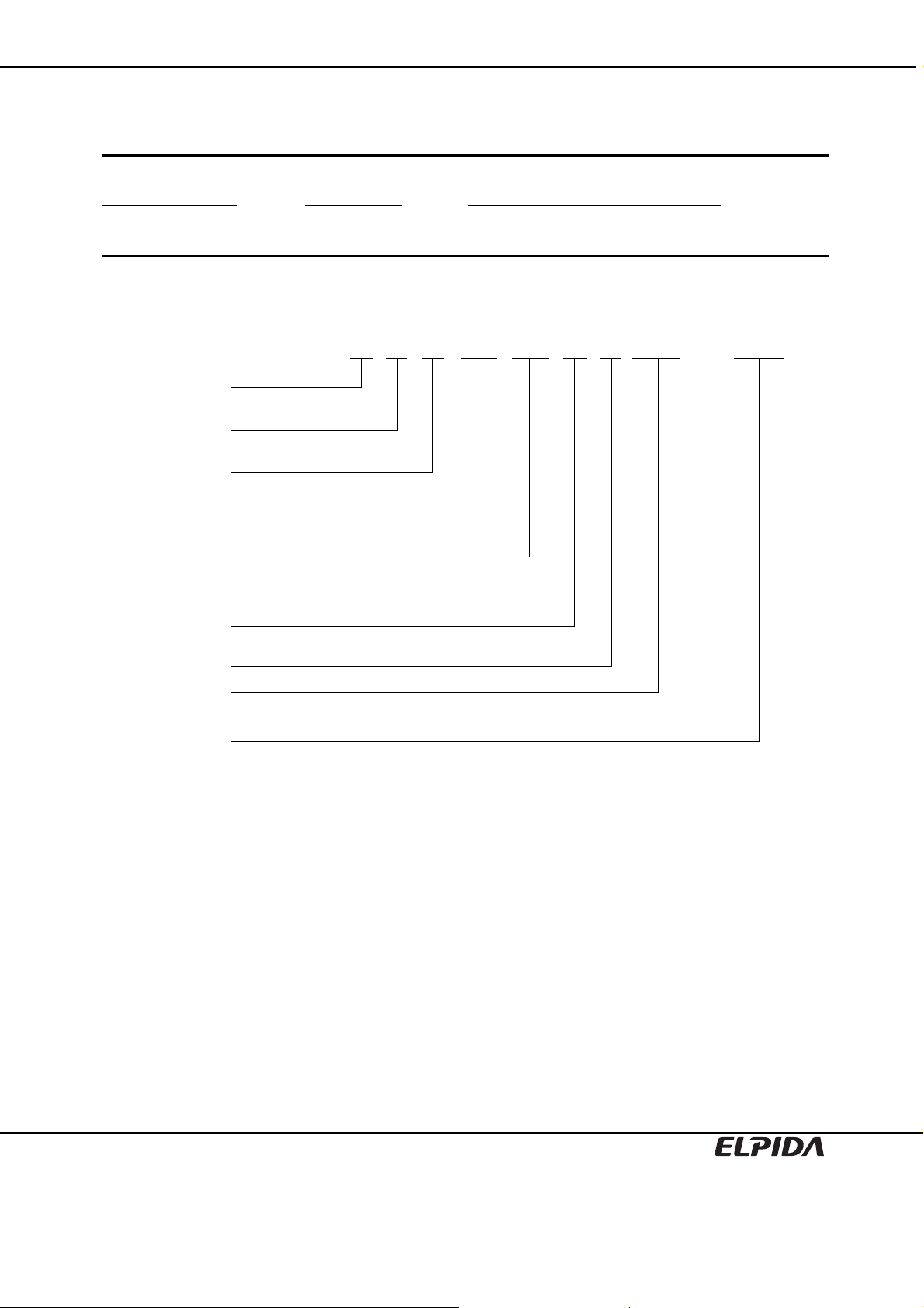
Part number
EDD5104ABTA-6B
EDD5104ABTA-7A
EDD5104ABTA-7B
EDD5108ABTA-6B
EDD5108ABTA-7A
EDD5108ABTA-7B
Part Number
Elpida Memory
Type
D: Monolithic Device
Product Code
D: DDR SDRAM
Mask
version
B 128M × 4 4
64M × 8
EDD5104ABTA, EDD5108ABTA
Organization
(words × bits)
Internal
banks
Data Rate
Mbps (max.)
333
266
266
333
266
266
JEDEC speed bin
(CL-tRCD-tRP)
DDR333B (2.5-3-3)
DDR266A (2-3-3)
DDR266B (2.5-3-3)
DDR333B (2.5-3-3)
DDR266A (2-3-3)
DDR266B (2.5-3-3)
E D D 51 04 A B TA - 6B
Package
66-pin Plastic
TSOP (II)
10.16mm(400)
Density / Bank
51: 512M / 4 banks
Bit Organization
4: x4
8: x8
Voltage, Interface
A: 2.5V, SSTL_2
Die Rev.
Package
TA: TSOP (II)
Speed
6B: DDR333B (2.5-3-3)
7A: DDR266A (2-3-3)
7B: DDR266B (2.5-3-3)
Preliminary Data Sheet E0237E30 (Ver. 3.0)
2

CONTENTS
EDD5104ABTA, EDD5108ABTA
Description.....................................................................................................................................................1
Features.........................................................................................................................................................1
Pin Configurations .........................................................................................................................................1
Ordering Information......................................................................................................................................2
Part Number ..................................................................................................................................................2
Electrical Specifications.................................................................................................................................4
Block Diagram .............................................................................................................................................10
Pin Function.................................................................................................................................................11
Command Operation ...................................................................................................................................13
Simplified State Diagram .............................................................................................................................21
Operation of the DDR SDRAM ....................................................................................................................22
Timing Waveforms.......................................................................................................................................41
Package Drawing ........................................................................................................................................47
Recommended Soldering Conditions ..........................................................................................................48
Preliminary Data Sheet E0237E30 (Ver. 3.0)
3
EDD5104ABTA, EDD5108ABTA
Electrical Specifications
• All voltages are referenced to VSS (GND).
• After power up, wait more than 200 µs and then, execute power on sequence and CBR (Auto) refresh before
proper device operation is achieved.
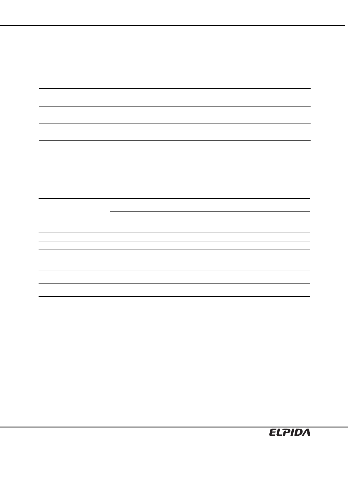
Absolute Maximum Ratings
Parameter Symbol Rating Unit Note
Voltage on any pin relative to VSS VT –1.0 to +3.6 V
Supply voltage relative to VSS VDD –1.0 to +3.6 V
Short circuit output current IOS 50 mA
Power dissipation PD 1.0 W
Operating temperature TA 0 to +70 °C
Storage temperature Tstg –55 to +125 °C
Caution
Exposing the device to stress above those listed in Absolute Maximum Ratings could cause
permanent damage. The device is not meant to be operated under conditions outside the limits
described in the operational section of this specification. Exposure to Absolute Maximum Rating
conditions for extended periods may affect device reliability.
Recommended Operating Conditions (TA = 0 to 70°°°°C)
Parameter Symbol Min Typ Max Unit Notes
Supply voltage
Input reference voltage VREF 0.49 × VDDQ 0.50 × VDDQ 0.51 × VDDQ V
Termination voltage VTT VREF – 0.04 VREF VREF + 0.04 V
Input high voltage VIH (DC) VREF + 0.15 — VDDQ + 0.3 V 2
Input low voltage VIL (DC) –0.3 — VREF – 0.15 V 3
Input voltage level,
CK and /CK inputs
Input differential cross point
voltage, CK and /CK inputs
Input differential voltage,
CK and /CK inputs
VDD,
VDDQ
VSS,
VSSQ
VIN (DC) –0.3 — VDDQ + 0.3 V 4
VIX (DC) 0.5 × VDDQ − 0.2V 0.5 × VDDQ 0.5 × VDDQ + 0.2V V
VID (DC) 0.36 — VDDQ + 0.6 V 5, 6
2.3 2.5 2.7 V 1
0 0 0 V
Notes: 1. VDDQ must be lower than or equal to VDD.
2. VIH is allowed to exceed VDD up to 3.6V for the period shorter than or equal to 5ns.
3. VIL is allowed to outreach below VSS down to –1.0V for the period shorter than or equal to 5ns.
4. VIN (DC) specifies the allowable dc execution of each differential input.
5. VID (DC) specifies the input differential voltage required for switching.
6. VIH (CK) min assumed over VREF + 0.18V, VIL (CK) max assumed under VREF – 0.18V
if measurement.
Preliminary Data Sheet E0237E30 (Ver. 3.0)
4

EDD5104ABTA, EDD5108ABTA
DC Characteristics 1 (TA = 0 to +70°°°°C, VDD, VDDQ = 2.5V ± 0.2V, VSS, VSSQ = 0V)
max.
Parameter Symbol Grade × 4 × 8 Unit Test condition Notes
Operating current (ACT-PRE) IDD0
Operating current
(ACT-READ-PRE)
Idle power down standby
current
Floating idle standby current IDD2F
Quiet idle standby current IDD2Q 25 25 mA
Active power down standby
current
Active standby current IDD3N
Operating current
(Burst read operation)
Operating current
(Burst write operation)
Auto Refresh current IDD5
Self refresh current IDD6 4 4 mA
Operating current
(4 banks interleaving)
IDD1
IDD2P 3 3 mA CKE ≤ VIL 4
IDD3P 20 20 mA CKE ≤ VIL 3
IDD4R
IDD4W
IDD7A
-6B
-7A, -7B
-6B
-7A, -7B
-6B
-7A, -7B
-6B
-7A, -7B
-6B
-7A, -7B
-6B
-7A, -7B
-6B
-7A, -7B
-6B
-7A, -7B
Notes: 1. These IDD data are measured under condition that DQ pins are not connected.
2. One bank operation.
3. One bank active.
4. All banks idle.
5. Command/Address transition once per one clock cycle.
6. DQ, DM and DQS transition twice per one clock cycle.
7. 4 banks active. Only one bank is running at tRC = tRC (min.)
8. The IDD data on this table are measured with regard to tCK = tCK (min.) in general.
9. Command/Address transition once every two clock cycles.
10. Command/Address stable at ≥ VIH or ≤ VIL.
150
135
170
155
40
35
70
60
200
170
200
170
290
270
420
360
150
135
180
160
40
35
70
60
210
180
210
180
290
270
430
370
CKE ≥ VIH,
mA
tRC = tRC (min.)
CKE ≥ VIH, BL = 4,
mA
CL = 2.5,
tRC = tRC (min.)
CKE ≥ VIH, /CS ≥ VIH,
mA
DQ, DQS, DM = VREF
CKE ≥ VIH, /CS ≥ VIH,
DQ, DQS, DM = VREF
CKE ≥ VIH, /CS ≥ VIH
mA
tRAS = tRAS (max.)
CKE ≥ VIH, BL = 2,
mA
CL = 2.5
CKE ≥ VIH, BL = 2,
mA
CL = 2.5
tRFC = tRFC (min.),
mA
Input ≤ VIL or ≥ VIH
Input ≥ VDD – 0.2 V
Input ≤ 0.2 V
mA BL = 4 5, 6, 7
1, 2, 9
1, 2, 5
4, 5
4, 10
3, 5, 6
1, 2, 5,
6
1, 2, 5,
6
DC Characteristics 2 (TA = 0 to +70°°°°C, VDD, VDDQ = 2.5V ± 0.2V, VSS, VSSQ = 0V)
Parameter Symbol min. max. Unit Test condition Notes
Input leakage current IL –2 2 µA VDD ≥ VIN ≥ VSS
Output leakage current IOZ –5 5 µA VDDQ ≥ VOUT ≥ VSS
Output high current IOH –15.2 — mA VOUT = 1.95V
Output low current IOL 15.2 — mA VOUT = 0.35V
Preliminary Data Sheet E0237E30 (Ver. 3.0)
5

EDD5104ABTA, EDD5108ABTA
Pin Capacitance (TA = +25°C, VDD, VDDQ = 2.5V ± 0.2V)
Parameter Symbol Pins min. Typ max. Unit Notes
Input capacitance CI1 CK, /CK 2.0 — 3.0 pF 1
CI2 All other input pins 2.0 — 3.0 pF 1
Delta input capacitance Cdi1 CK, /CK — — 0.25 pF 1
Cdi2 All other input-only pins — — 0.5 pF 1
Data input/output capacitance CI/O DQ, DM, DQS 4.0 — 5 pF 1, 2,
Delta input/output capacitance Cdio DQ, DM, DQS — — 0.5 pF 1
Notes: 1. These parameters are measured on conditions: f = 100MHz, VOUT = VDDQ/2, ∆VOUT = 0.2V,
TA = +25°C.
2. DOUT circuits are disabled.
AC Characteristics (TA = 0 to +70°°°°C, VDD, VDDQ = 2.5V ± 0.2V, VSS, VSSQ = 0V)
-6B -7A -7B
Parameter Symbol
Clock cycle time
(CL = 2)
(CL = 2.5) tCK 6 12 7.5 12 7.5 12 ns
CK high-level width tCH 0.45 0.55 0.45 0.55 0.45 0.55 tCK
CK low-level width tCL 0.45 0.55 0.45 0.55 0.45 0.55 tCK
CK half period tHP
DQ output access time from
CK, /CK
DQS output access time from CK,
/CK
DQS to DQ skew tDQSQ — 0.45 — 0.5 — 0.5 ns 3
DQ/DQS output hold time from DQS tQH tHP – tQHS — tHP – tQHS — tHP – tQHS — ns
Data hold skew factor tQHS — 0.55 — 0.75 — 0.75 ns
Data-out high-impedance time from
CK, /CK
Data-out low-impedance time from
CK, /CK
Read preamble tRPRE 0.9 1.1 0.9 1.1 0.9 1.1 tCK
Read postamble tRPST 0.4 0.6 0.4 0.6 0.4 0.6 tCK
DQ and DM input setup time tDS 0.45 — 0.5 — 0.5 — ns 8
DQ and DM input hold time tDH 0.45 — 0.5 — 0.5 — ns 8
DQ and DM input pulse width tDIPW 1.75 — 1.75 — 1.75 — ns 7
Write preamble setup time
Write preamble tWPRE 0.25 — 0.25 — 0.25 — tCK
Write postamble tWPST 0.4 0.6 0.4 0.6 0.4 0.6 tCK 9
Write command to first DQS latching
transition
DQS falling edge to CK setup time tDSS 0.2 — 0.2 — 0.2 — tCK
DQS falling edge hold time from CK tDSH 0.2 — 0.2 — 0.2 — tCK
DQS input high pulse width tDQSH 0.35 — 0.35 — 0.35 — tCK
DQS input low pulse width tDQSL 0.35 0.35 — 0.35 — tCK
tCK 7.5 12 7.5 12 10 12 ns 10
tAC –0.7 0.7 –0.75 0.75 –0.75 0.75 ns 2, 11
tDQSC
K
tHZ –0.7 0.7 –0.75 0.75 –0.75 0.75 ns 5, 11
tLZ –0.7 0.7 –0.75 0.75 –0.75 0.75 ns 6, 11
tWPRE
S
tDQSS 0.75 1.25 0.75 1.25 0.75 1.25 tCK
min. max. min. max min. max.
min
(tCH, tCL)
–0.6 0.6 –0.75 0.75 –0.75 0.75 ns 2, 11
0 — 0 — 0 — ns
—
min
(tCH, tCL)
—
min
(tCH, tCL)
— tCK
Unit Notes
Preliminary Data Sheet E0237E30 (Ver. 3.0)
6

EDD5104ABTA, EDD5108ABTA
-6B -7A -7B
Parameter Symbol
Address and control input setup time tIS 0.75 — 0.9 — 0.9 —
Address and control input hold time tIH 0.75 — 0.9 — 0.9 — ns 8
Address and control input pulse
width
Mode register set command cycle
time
Active to Precharge command
period
Active to Active/Auto refresh
command period
Auto refresh to Active/Auto refresh
command period
Active to Read/Write delay tRCD 18 — 20 — 20 — ns
Precharge to active command period tRP 18 — 20 — 20 — ns
Active to Autoprecharge delay tRAP tRCD min. — tRCD min. — tRCD min. — ns
Active to active command period tRRD 12 — 15 — 15 — ns
Write recovery time tWR 15 — 15 — 15 — ns
Auto precharge write recovery and
precharge time
Internal write to Read command
delay
Average periodic refresh interval tREF — 7.8 — 7.8 — 7.8 µs
tIPW 2.2 — 2.2 — 2.2 — ns 7
tMRD 2 — 2 — 2 — tCK
tRAS 42 120000 45 120000 45 120000 ns
tRC 60 — 67.5 — 67.5 — ns
tRFC 72 — 75 — 75 — ns
tDAL
tWTR 1 — 1 — 1 — tCK
Notes: 1. On all AC measurements, we assume the test conditions shown in the next page. For timing parameter
definitions, see ‘Timing Waveforms’ section.
2. This parameter defines the signal transition delay from the cross point of CK and /CK. The signal
transition is defined to occur when the signal level crossing VTT.
3. The timing reference level is VTT.
4. Output valid window is defined to be the period between two successive transition of data out or DQS
(read) signals. The signal transition is defined to occur when the signal level crossing VTT.
5. tHZ is defined as DOUT transition delay from Low-Z to High-Z at the end of read burst operation. The
timing reference is cross point of CK and /CK. This parameter is not referred to a specific DOUT voltage
level, but specify when the device output stops driving.
6. tLZ is defined as DOUT transition delay from High-Z to Low-Z at the beginning of read operation. This
parameter is not referred to a specific DOUT voltage level, but specify when the device output begins
driving.
7. Input valid windows is defined to be the period between two successive transition of data input or DQS
(write) signals. The signal transition is defined to occur when the signal level crossing VREF.
8. The timing reference level is VREF.
9. The transition from Low-Z to High-Z is defined to occur when the device output stops driving. A specific
reference voltage to judge this transition is not given.
10. tCK (max.) is determined by the lock range of the DLL. Beyond this lock range, the DLL operation is not
assured.
11. tCK = tCK (min.) when these parameters are measured. Otherwise, absolute minimum values of these
values are 10% of tCK.
12. VDD is assumed to be 2.5V ± 0.2V. VDD power supply variation per cycle expected to be less than
0.4V/400 cycle.
13. tDAL = (tWR/tCK)+(tRP/tCK)
For each of the terms above, if not already an integer, round to the next highest integer.
Example: For –7A Speed at CL = 2.5, tCK = 7.5ns, tWR = 15ns and tRP= 20ns,
tDAL = (15ns/7.5ns) + (20ns/7.5ns) = (2) + (3)
tDAL = 5 clocks
min. max. min. max min. max.
(tWR/tCK)+
(tRP/tCK)
(tWR/tCK)+
(tRP/tCK)
—
(tWR/tCK)+
(tRP/tCK)
— tCK 13
Unit Notes
Preliminary Data Sheet E0237E30 (Ver. 3.0)
7
EDD5104ABTA, EDD5108ABTA
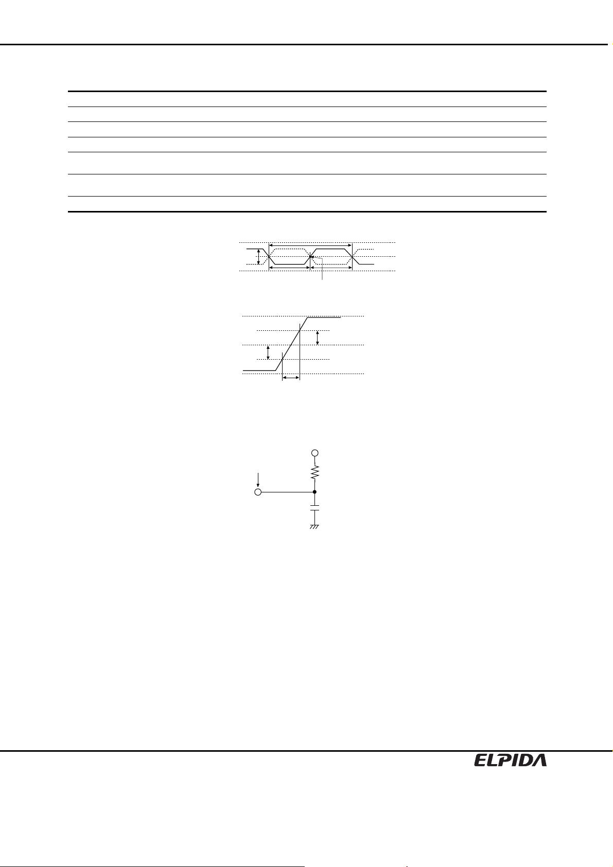
Test Conditions
Parameter Symbol Value Unit
Input reference voltage VREF VDDQ/2 V
Termination voltage VTT VREF V
Input high voltage VIH (AC) VREF + 0.31 V
Input low voltage VIL (AC) VREF − 0.31 V
Input differential voltage, CK and /CK
inputs
Input differential cross point voltage,
CK and /CK inputs
Input signal slew rate SLEW 1 V/ns
CK
/CK
VID (AC) 0.62 V
VIX (AC) VREF V
VID
tCL
tCK
tCH
VDD
VREF
VSS
VIX
VDD
VIH
VIL
∆t
SLEW = (VIH (AC) – VIL (AC))/∆t
VTT
Measurement point
RT = 50Ω
DQ
CL = 30pF
Input Waveforms and Output Load
VREF
VSS
Preliminary Data Sheet E0237E30 (Ver. 3.0)
8
EDD5104ABTA, EDD5108ABTA
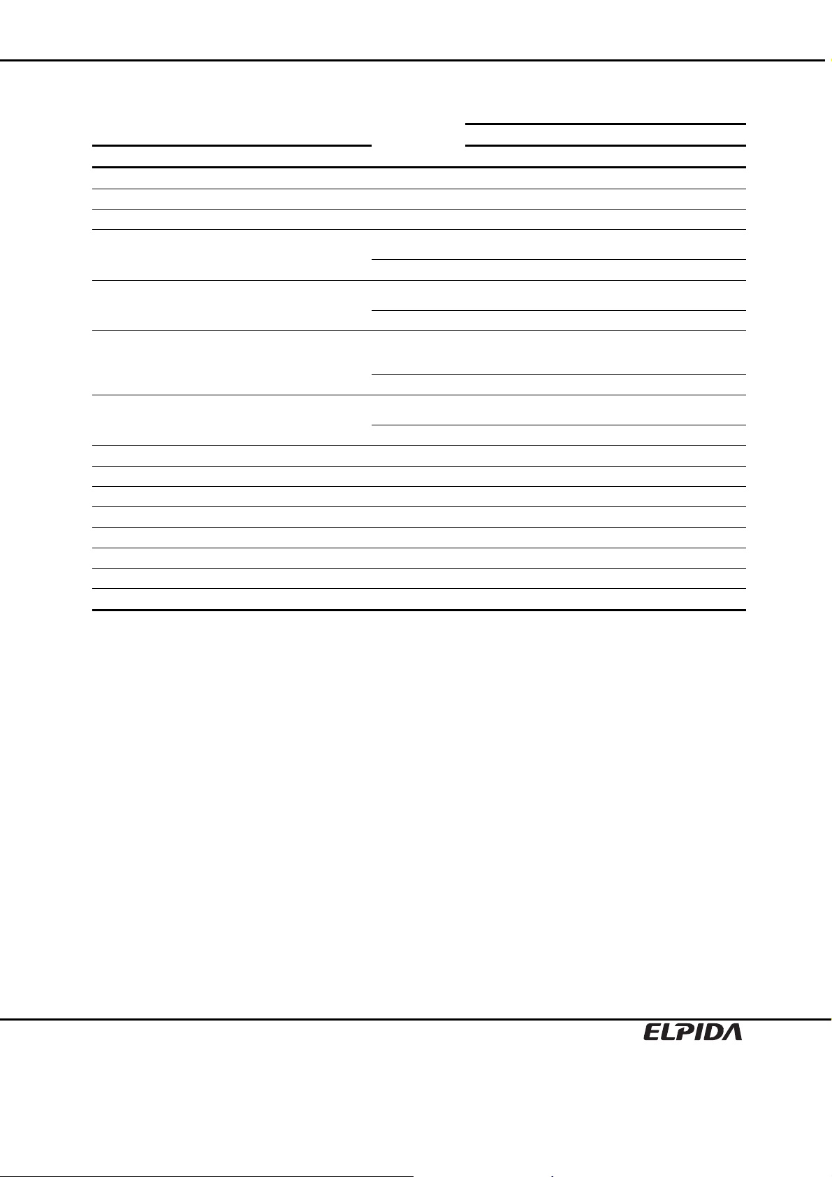
Timing Parameter Measured in Clock Cycle
Number of clock cycle
tCK 6ns 7.5ns
Parameter Symbol min. max. min. max.
Write to pre-charge command delay (same bank) tWPD 4 + BL/2 3 + BL/2
Read to pre-charge command delay (same bank) tRPD BL/2 BL/2
Write to read command delay (to input all data) tWRD 2 + BL/2 2 + BL/2
Burst stop command to write command delay
(CL = 2)
(CL = 2.5) tBSTW 3 3
Burst stop command to DQ High-Z
(CL = 2)
(CL = 2.5) tBSTZ 2.5 2.5 2.5 2.5
Read command to write command delay
(to output all data)
(CL = 2)
(CL = 2.5) tRWD 3 + BL/2 3 + BL/2
Pre-charge command to High-Z
(CL = 2)
(CL = 2.5) tHZP 2.5 2.5 2.5 2.5
Write command to data in latency tWCD 1 1 1 1
Write recovery time tWR 3 2
DM to data in latency tDMD 0 0 0 0
Mode register set command cycle time tMRD 2 2
Self refresh exit to non-read command tSNR 12 10
Self refresh exit to read command tSRD 200 200
Power down entry tPDEN 1 1 1 1
Power down exit to command input tPDEX 1 1
tBSTW 2 2
tBSTZ 2 2 2 2
tRWD 2 + BL/2 2 + BL/2
tHZP 2 2 2 2
Preliminary Data Sheet E0237E30 (Ver. 3.0)
9
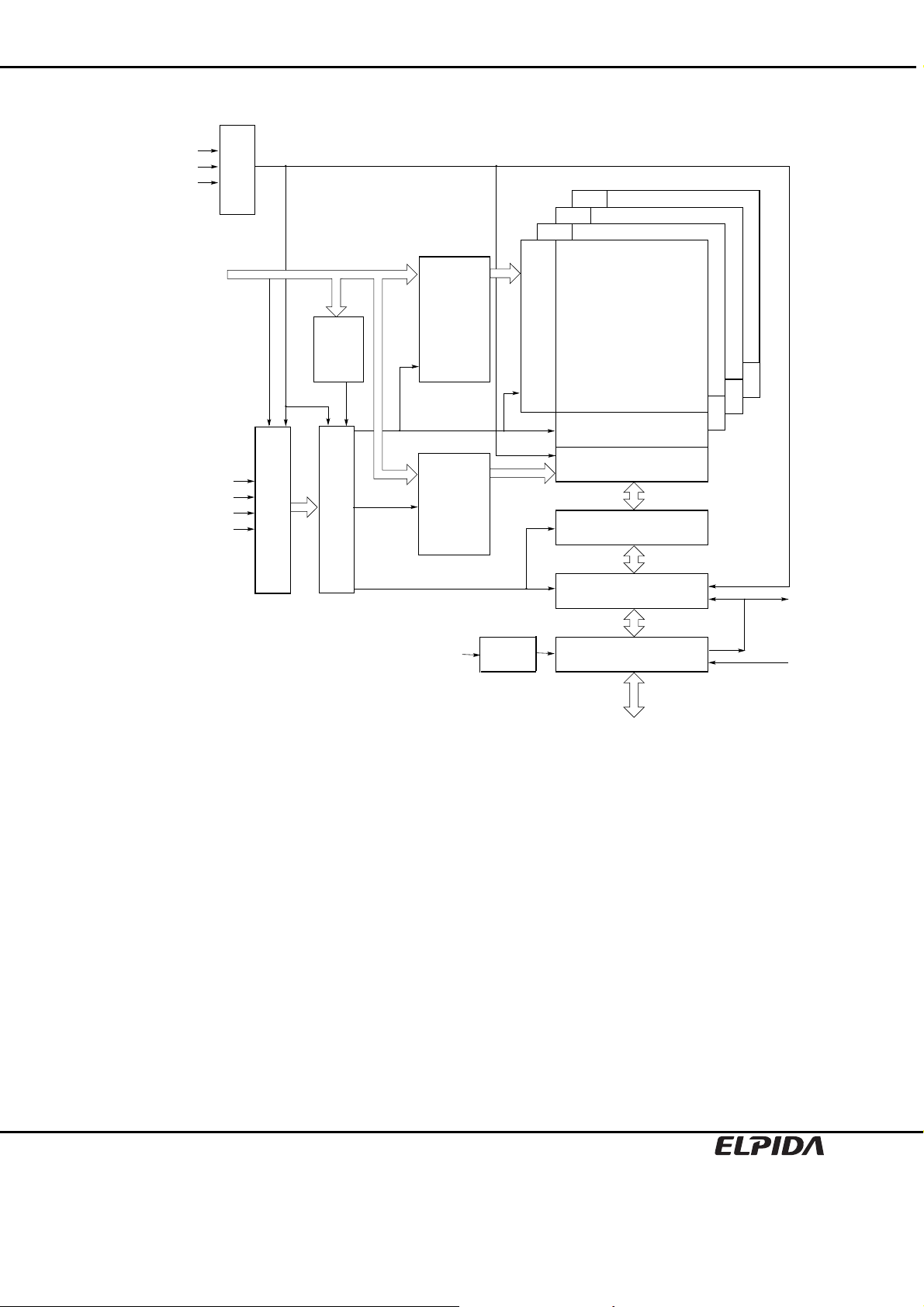
Block Diagram
CK
/CK
CKE
Clock
generator
EDD5104ABTA, EDD5108ABTA
Bank 3
Bank 2
Bank 1
A0 to A12, BA0, BA1
/RAS
/CAS
/CS
/WE
Mode
register
Control logic
Command decoder
Row
address
buffer
and
refresh
counter
Column
address
buffer
and
burst
counter
CK, /CK
DLL
Memory cell array
Row decoder
Sense amp.
Column decoder
Data control circuit
Latch circuit
Input & Output buffer
Bank 0
DQS
DM
DQ
Preliminary Data Sheet E0237E30 (Ver. 3.0)
10
EDD5104ABTA, EDD5108ABTA
Pin Function
CK, /CK (input pins)
The CK and the /CK are the master clock inputs. All inputs except DM, DQS and DQs are referred to the cross point
of the CK rising edge and the /CK falling edge. When a read operation, DQS and DQs are referred to the cross point
of the CK and the /CK. When a write operation, DQS and DQs are referred to the cross point of the DQS and the
VREF level. DQS for write operation is referred to the cross point of the CK and the /CK. CK is the master clock
input to this pin. The other input signals are referred at CK rising edge.
/CS (input pin)
When /CS is Low, commands and data can be input. When /CS is High, all inputs are ignored. However, internal
operations (bank active, burst operations, etc.) are held.
/RAS, /CAS, and /WE (input pins)
These pins define operating commands (read, write, etc.) depending on the combinations of their voltage levels.
See "Command operation".
A0 toA12 (input pins)
Row address (AX0 to AX12) is determined by the A0 to the A12 level at the cross point of the CK rising edge and the
/CK falling edge in a bank active command cycle. Column address (See “Address Pins Table”) is loaded via the A0
to the A9, A11 and A12 at the cross point of the CK rising edge and the /CK falling edge in a read or a write
command cycle. This column address becomes the starting address of a burst operation.
[Address Pins Table]
Address (A0 to A12)
Part number Row address Column address
EDD5104AB AX0 to AX12 AY0 to AY9, AY11, AY12
EDD5108AB AX0 to AX12 AY0 to AY9, AY11,
A10 (AP) (input pin)
A10 defines the precharge mode when a precharge command, a read command or a write command is issued. If
A10 = High when a precharge command is issued, all banks are precharged. If A10 = Low when a precharge
command is issued, only the bank that is selected by BA1/BA0 is precharged. If A10 = High when read or write
command, auto-precharge function is enabled. While A10 = Low, auto-precharge function is disabled.
BA0 and BA1 (input pins)
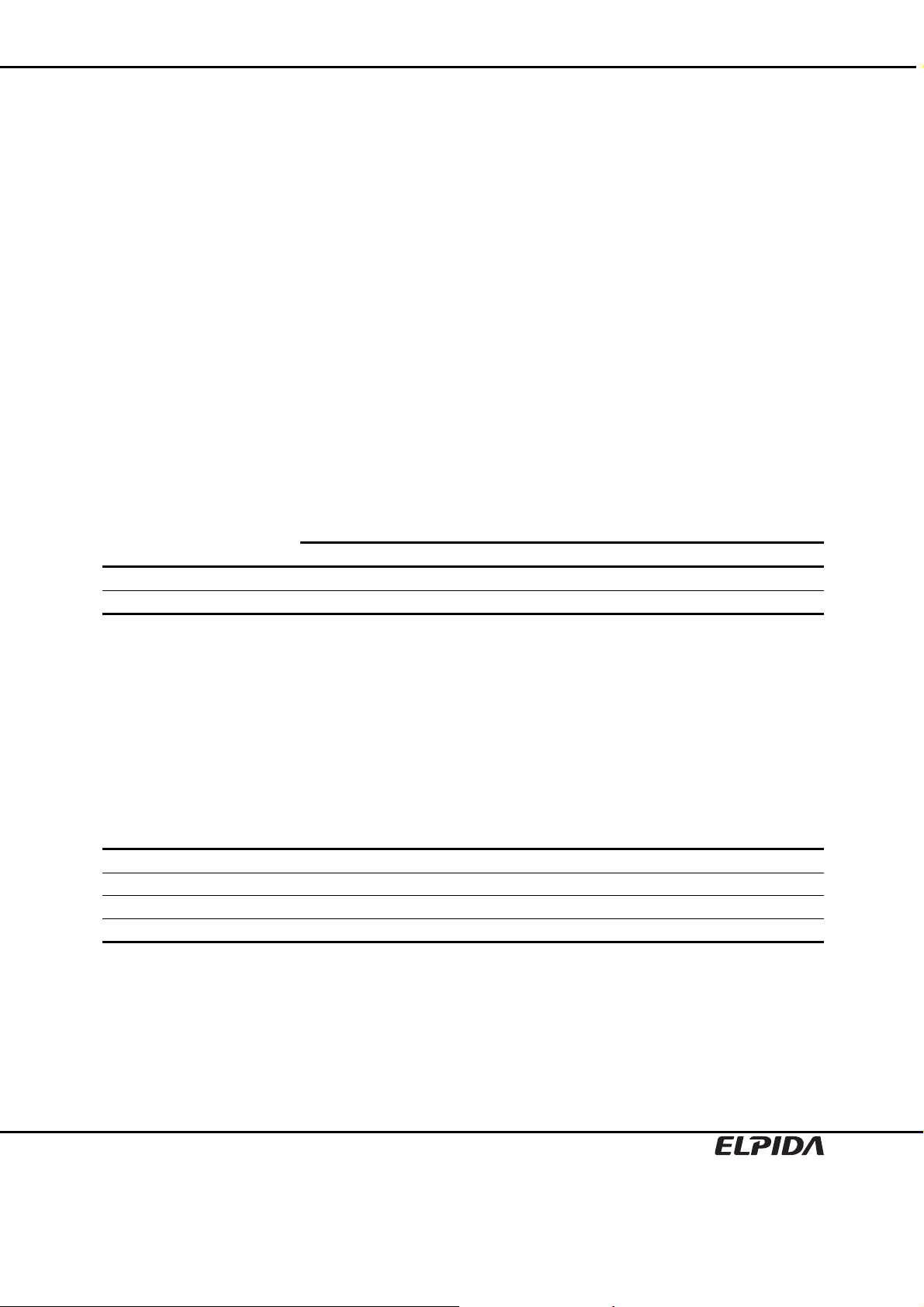
BA0, BA1 are bank select signals (BA). The memory array is divided into bank 0, bank 1, bank 2 and bank 3. (See
Bank Select Signal Table)
[Bank Select Signal Table]
BA0 BA1
Bank 0 L L
Bank 1 H L
Bank 2 L H
Bank 3 H H
Remark: H: VIH. L: VIL
Preliminary Data Sheet E0237E30 (Ver. 3.0)
11

EDD5104ABTA, EDD5108ABTA
CKE (input pin)
This pin determines whether or not the next CK is valid. If CKE is High, the next CK rising edge is valid. If CKE is
Low. CKE controls power down and self-refresh. The power down and the self-refresh commands are entered when
the CKE is driven Low and exited when it resumes to High. CKE must be maintained high throughout read or write
access.
The CKE level must be kept for 1 CK cycle at least, that is, if CKE changes at the cross point of the CK rising edge
and the /CK falling edge with proper setup time tIS, by the next CK rising edge CKE level must be kept with proper
hold time tIH.
DM (input pin)
DM is the reference signal of the data input mask function. DM is sampled at the cross point of DQS and VREF.
DQ0 toDQ7 (input/output pins)
Data is input to and output from these pins (DQ0 to DQ3; EDD5104AB, DQ0 to DQ7; EDD5108AB).
DQS (input and output pin): DQS provides the read data strobe (as output) and the write data strobe (as input).
VDD, VSS, VDDQ, VSSQ (Power supply)
VDD and VSS are power supply pins for internal circuits. VDDQ and VSSQ are power supply pins for the output
buffers.
Preliminary Data Sheet E0237E30 (Ver. 3.0)
12
EDD5104ABTA, EDD5108ABTA
Command Operation
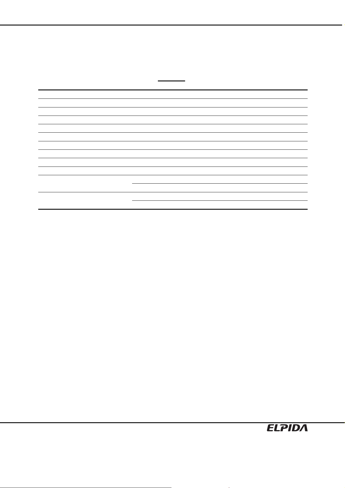
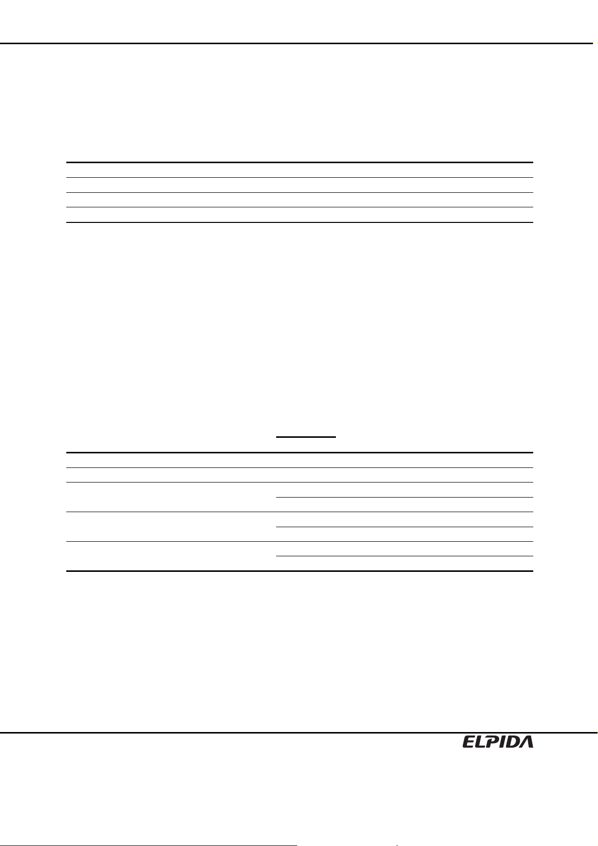
Command Truth Table
DDR SDRAM recognize the following commands specified by the /CS, /RAS, /CAS, /WE and address pins. All other
combinations than those in the table below are illegal.
CKE
Command Symbol n – 1 n /CS /RAS /CAS /WE BA1 BA0 AP Address
Ignore command DESL H H H × × × × × × ×
No operation NOP H H L H H H × × × ×
Burst stop in read command BST H H L H H L × × × ×
Column address and read command READ H H L H L H V V L V
Read with auto-precharge READA H H L H L H V V H V
Column address and write command WRIT H H L H L L V V L V
Write with auto-precharge WRITA H H L H L L V V H V
Row address strobe and bank active ACT H H L L H H V V V V
Precharge select bank PRE H H L L H L V V L ×
Precharge all bank PALL H H L L H L × × H ×
Refresh REF H H L L L H × × × ×
SELF H L L L L H × × × ×
Mode register set MRS H H L L L L L L L V
EMRS H H L L L L L H L V
Remark: H: VIH. L: VIL. ×: VIH or VIL V: Valid address input
Note: The CKE level must be kept for 1 CK cycle at least.
Ignore command [DESL]
When /CS is High at the cross point of the CK rising edge and the VREF level, every input are neglected and internal
status is held.
No operation [NOP]
As long as this command is input at the cross point of the CK rising edge and the VREF level, address and data
input are neglected and internal status is held.
Burst stop in read operation [BST]
This command stops a burst read operation, which is not applicable for a burst write operation.
Column address strobe and read command [READ]
This command starts a read operation. The start address of the burst read is determined by the column address
(See “Address Pins Table” in Pin Function) and the bank select address. After the completion of the read operation,
the output buffer becomes High-Z.
Read with auto-precharge [READA]
This command starts a read operation. After completion of the read operation, precharge is automatically executed.
Column address strobe and write command [WRIT]
This command starts a write operation. The start address of the burst write is determined by the column address
(See “Address Pins Table” in Pin Function) and the bank select address.
Write with auto-precharge [WRITA]
This command starts a write operation. After completion of the write operation, precharge is automatically executed.
Preliminary Data Sheet E0237E30 (Ver. 3.0)
13
EDD5104ABTA, EDD5108ABTA
Row address strobe and bank activate [ACT]
This command activates the bank that is selected by BA0, BA1 and determines the row address (AX0 to AX12).
(See Bank Select Signal Table)
Precharge selected bank [PRE]
This command starts precharge operation for the bank selected by BA0, BA1. (See Bank Select Signal Table)
[Bank Select Signal Table]
BA0 BA1
Bank 0 L L
Bank 1 H L
Bank 2 L H
Bank 3 H H
Remark: H: VIH. L: VIL
Precharge all banks [PALL]
This command starts a precharge operation for all banks.
Refresh [REF/SELF]
This command starts a refresh operation. There are two types of refresh operation, one is auto-refresh, and another
is self-refresh. For details, refer to the CKE truth table section.
Mode register set/Extended mode register set [MRS/EMRS]
The DDR SDRAM has the two mode registers, the mode register and the extended mode register, to defines how it
works. The both mode registers are set through the address pins (the A0 to the A12, BA0 to BA1) in the mode
register set cycle. For details, refer to "Mode register and extended mode register set".
CKE Truth Table
CKE
Current state Command n – 1 n /CS /RAS /CAS /WE Address Notes
Idle Auto-refresh command (REF) H H L L L H × 2
Idle Self-refresh entry (SELF) H L L L L H × 2
Idle Power down entry (PDEN) H L L H H H ×
H L H × × × ×
Self refresh Self refresh exit (SELFX) L H L H H H ×
L H H × × × ×
Power down Power down exit (PDEX) L H L H H H ×
L H H × × × ×
Remark: H: VIH. L: VIL. ×: VIH or VIL.
Notes: 1. All the banks must be in IDLE before executing this command.
2. The CKE level must be kept for 1 CK cycle at least.
Preliminary Data Sheet E0237E30 (Ver. 3.0)
14
EDD5104ABTA, EDD5108ABTA
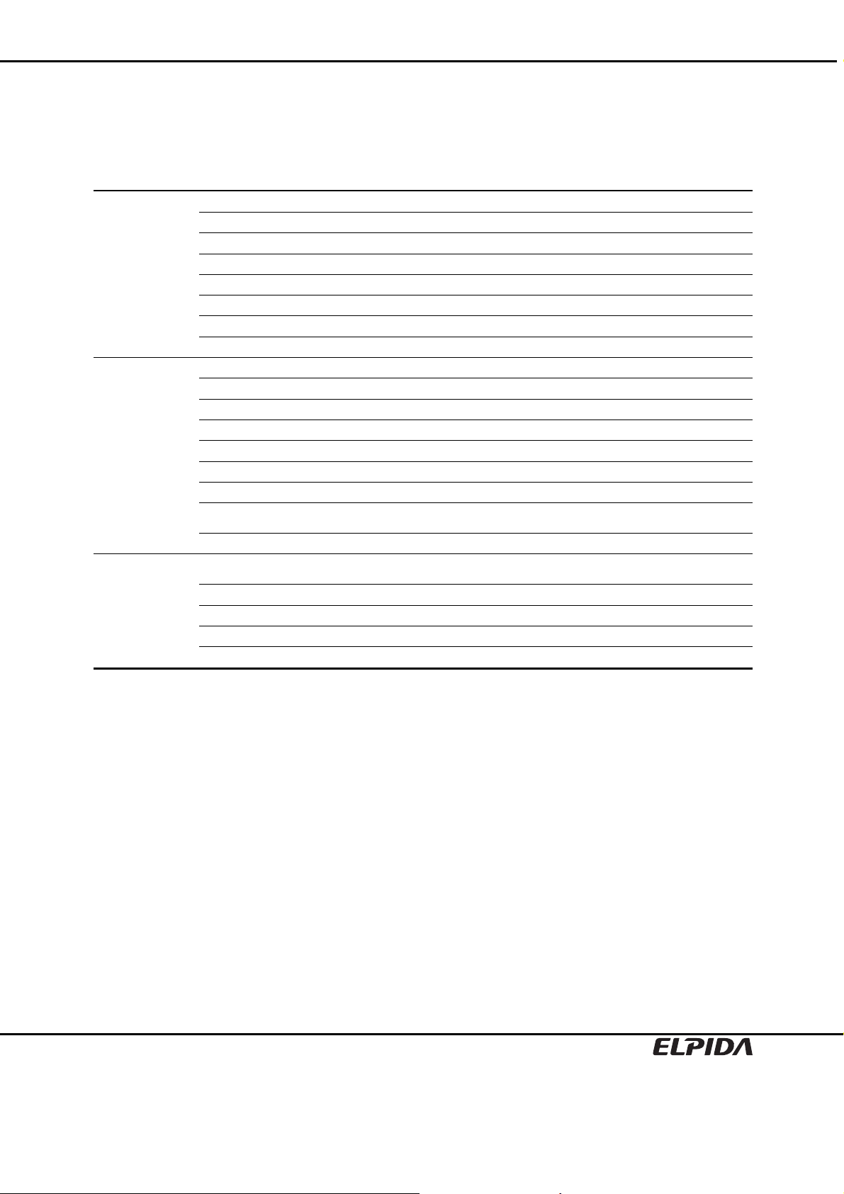
Function Truth Table
The following tables show the operations that are performed when each command is issued in each state of the
DDR SDRAM.
Function Truth Table (1)
Current state /CS /RAS /CAS /WE Address Command Operation Next state
1
Precharging*
L H H H × NOP NOP ldle
L H H L × BST ILLEGAL*
L H L H BA, CA, A10 READ/READA ILLEGAL*11 —
L H L L BA, CA, A10 WRIT/WRITA ILLEGAL*11 —
L L H H BA, RA ACT ILLEGAL*11 —
L L H L BA, A10 PRE, PALL NOP ldle
L L L × × ILLEGAL —
2
Idle*
H × × × × DESL NOP ldle
L H H H × NOP NOP ldle
L H H L × BST ILLEGAL*
L H L H BA, CA, A10 READ/READA ILLEGAL*11 —
L H L L BA, CA, A10 WRIT/WRITA ILLEGAL*11 —
L L H H BA, RA ACT Activating Active
L L H L BA, A10 PRE, PALL NOP ldle
L L L H × REF, SELF
L L L L MODE MRS Mode register set*12 ldle
Refresh
(auto-refresh)*
L H H H × NOP NOP ldle
L H H L × BST ILLEGAL —
L H L × × ILLEGAL —
L L × × × ILLEGAL —
H × × × × DESL NOP ldle
11
—
11
—
Refresh/
Self refresh*
H × × × × DESL NOP ldle
3
12
ldle/
Self refresh
Preliminary Data Sheet E0237E30 (Ver. 3.0)
15
 Loading...