

1
Rev.1.0
Parameter Symbol Limit Unit
VIN power supply voltage Vin -0.3 to +6.0 V
Apply voltage to SW Vsw GND-0.3 to Vout+0.3 V
Apply voltage to FB Vfb GND-0.3 to Vout+0.3 V
Apply voltage to EN Ven GND-0.3 to Vout+0.3 V
Apply voltage to VOUT Vout -0.3 to +6.0 V
Power dissipation Pd 250 mW
Operating temperature range Top -30 to +85 °C
Storage temperature range Tstg -65 to 125 °C
■General description
■Features
■Maximum absolute ratings
• Cellular phone
• Digital camera
• MP3 player
• Portable machine
• Wireless handset
■Application
10 -
• Current mode control
• Output voltage drop protection
• Thermal shutdown protection and short circuit protection
• Input voltage
: 0.6V to 5.0V
• Output voltage
: 2.5V to 6.0V
• Low current consumption
: Typ.300µA
• Shutdown current
: < 1µA
• Low start-up voltage
: Typ.0.9V
• Low switch on (internal switch) resistance : 0.35Ω
• Constant frequency
: Typ.1.4MHz
• High efficiency
: 96%
• Package
: SOT-26
ELM620BA is synchronous PWM step-up DC/DC converter with high efficiency and 1.4MHz fixed frequency;
by adopting synchronous switch, ELM620BA is able to provide high efficiency without external Schottky diode.
ELM620BA is able to activate within the range from 0.6V to 5V of input voltage and 2.5V to 6V of output one.
For 3V or 3.3V output, ELM620BA can provide current up to 260mA by a single AA cell, or to 600mA by 2
serial-connected AA cells.
With 1.4MHz switching frequency, small coils and capacitors can be adopted; therefore, ELM620BA is possible
to be assembled within small areas on the board .
Caution:Permanent damage to the device may occur when ratings above maximum absolute ones are used.
*
Taping direction is one way.
ELM620BA-S
Symbol
a Package B: SOT-26
b Product version A
c Taping direction S: Refer to PKG file
ELM620BA - S
↑ ↑
↑
a b
c
■Selection guide
ELM620BA
1.4MHz
high efficiency synchronous PWM step up DC/DC converter

2
Rev.1.0
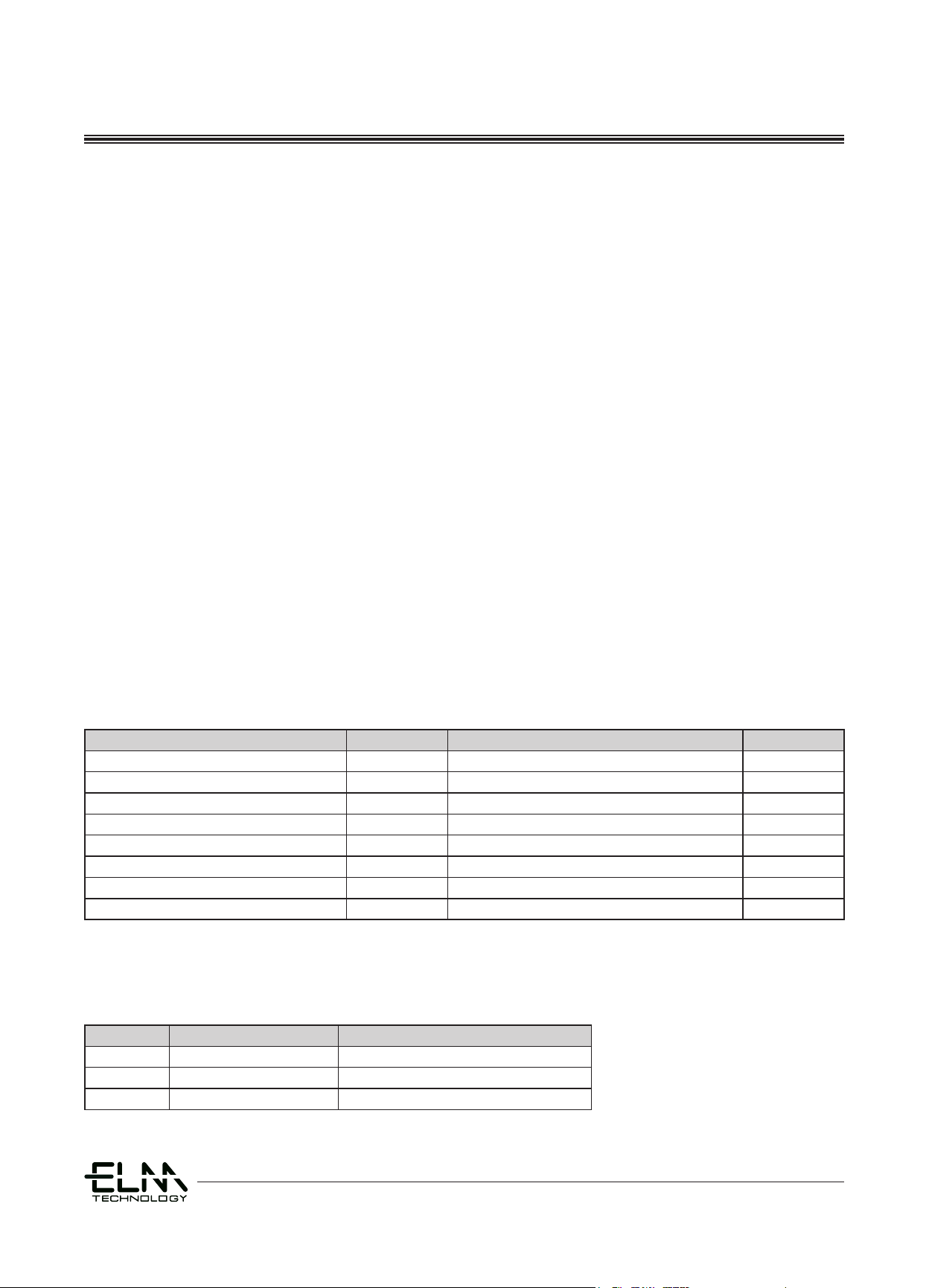
■Pin assignment
1) SW (Pin 1) : Switch pin.
Connect inductor between SW and VIN. Keep these PCB trace lengths as short and wide as possible to reduce
EMI and voltage overshoot.
2) GND (Pin 2) : Signal and power ground.
Provide a short direct PCB path between GND and the (−) side of output capacitor(s).
3) FB (Pin 3) : Feedback input to gm error amplifier.
Connect resistor divider tap to this pin. The output voltage can be adjusted from 2.5V to 6V by :
Vout = 1.203V × (1 +
R1
)
R2
4) EN (Pin 4) : Logic controlled shutdown input.
EN = High: Normal free running operation, 1.4MHz typical operating frequency. EN = Low: Shutdown, quiescent current < 1μA. Output capacitor can be completely discharged through the load or feedback resistors.
5) VOUT (Pin 5) : Output voltage sense input and drain of internal synchronous rectifier MOSFET.
Bias is derived from Vout. PCB trace length from Vout to output filter capacitor(s) should be as short and wide
as possible.
6) VIN (Pin 6) : Battery input voltage.
The device gets its start-up bias from Vin. Once Vout exceeds Vin, bias comes from Vout. Thus, once operation
is started, it is completely independent from Vin and only limited by output power level and battery’s internal
series resistance.
SOT-26(TOP VIEW)
1
2
3
6
5
4
■Pin configuration
Pin No. Pin name Pin description
1 SW Switch
2 GND Ground
3 FB Feedback
4 EN ON/OFF control (High enable)
5 VOUT Output
6 VIN Input
10 -
ELM620BA
1.4MHz
high efficiency synchronous PWM step up DC/DC converter
3
Rev.1.0
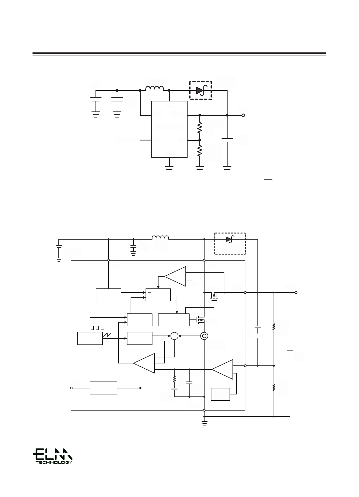
■Block diagram
+
+
+
optional
EN
SW
Vin
FB
Vout
GND
Optional
schottky
L
2.2µH
Cin
22µF
1V to 5V
Input
Vout
1.203V
ref
R1
1.02M
1%
R2
604k
1%
Cff
Cout
22µF
0.45Ω
0.35Ω
Current
sense
g
m
error
AMP
PWM
comp
PWM
control
Slope
comp
Sync drive
control
Ramp Gen
1.4MHz
Shutdown
control
Shutdown
ELM620BA
Start-up
OSC
A/B MUX
A
B
2.3V
Rc
80k
Cp
2
2.5pF
Cc
150pF
Vout
good
■Standard circuit
+
FB
VOUT
GND
VIN
ELM620BA
Vin
Optional
schottky
Vout
SW
EN
ON/OFF
L=2.2µH
Cin=
22µF
Cout
22µF
R1=
1.02MΩ
1%
R2
604k
Ω
1%
R1
Vout=(1+ )×1.203
R2
10 -
ELM620BA
1.4MHz
high efficiency synchronous PWM step up DC/DC converter
4
Rev.1.0
Parameter Symbol Condition Min. Typ. Max. Unit
Output voltage range (adj.) Vout 2.5 6.0 V
Minimum start-up voltage Vst Iload=1mA 0.9 1.1 V
Minimum operating voltage Vin EN=Vin 0.60 0.75 V
Switching frequency Fsw 1.1 1.4 1.7 MHz
Maximum duty cycle Dmax Vfb=1.15V 80 87 %
Current limit delay to output tllimdly 40 ns
Feedback voltage Vfb 1.165 1.203 1.241 V
Feedback input current Ifb Vfb=1.22V 1 nA
NMOS switch leakage IleakN Vsw=5V 0.1 5.0 µA
PMOS switch leakage
IleakP
Vsw=0V 0.1 5.0 µA
NMOS switch ON resistance
RswN
Vout=3.3V 0.35 Ω
PMOS switch ON resistance
RswP
Vout=3.3V 0.45 Ω
NMOS current limit IlimN 700 950 mA
Quiescent current (Active) Iq Measured on Vout, Non-switching 300 500 µA
Shutdown current Is Ven=0V, Including switch leakage 0.1 1.0 µA
EN input high Venh 1 V
EN input low Venl 0.35 V
EN input current Ien Ven=5.5V 0.01 1.00 µA
■Electrical characteristics
Vin=1.2V, Vout=3.3V, Top=25°C, unless otherwise noted
10 -
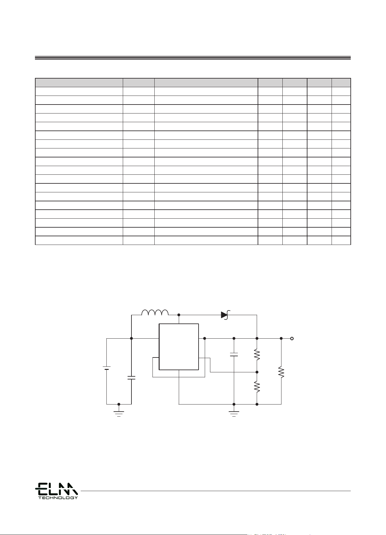
■Test circuits
V
I
N
S
W
F
B
L
=
2
.
2
µ
H
E
N
G
N
D
E
L
M
6
2
0
B
A
V
O
U
T
S
B
D
R
2
R
1
R
L
V
o
u
t
C
i
n
=
2
2
µ
F
V
i
n
C
o
u
t
=
2
2
µ
F
ELM620BA
1.4MHz
high efficiency synchronous PWM step up DC/DC converter

5
Rev.1.0
■Application notes
3
EN
Vout
Vin
1
2
6
5
4
SW
VIN
GND
FB EN
VOUT
Figure 1: Recommended component placement for single layer board with optional Schottky diode. Traces carrying high current are direct. Trace area at FB pin is small. Lead length to battery is short.
2) Inductor selection
ELM620BA can utilize small surface mount and chip inductors due to its fast 1.4MHz switching frequency.
Typically, a 2.2μH inductor is recommended for most applications; larger values of inductance will allow greater output current capability by reducing the inductor ripple current. Increasing the inductance above 10μH will
increase size while providing little improvement in output current capability.
Iout(max) = η × (Ip −
Vin×D )
× (1 − D)
2×f×L
where:
η = estimated efficiency Ip = peak current limit value (0.7A)
Vin = input (battery) voltage
D = steady-state duty ratio = (Vout − Vin) / Vout
f = switching frequency (1.4MHz typical)
L = inductance value
The inductor current ripple is typically set for 20% to 40% of the maximum inductor current (IP). High frequency ferrite core inductor materials reduce frequency dependent power losses compared to cheaper powdered
iron types. The inductor should have low ESR (series resistance of the windings) to reduce the I2R power losses,
and must be able to handle the peak inductor current without saturating. Molded chokes and some chip inductors usually do not have enough core to support the peak inductor currents of 950mA seen on ELM620BA. To
minimize radiated noise, ELM recommends using a toroid, pot core or shielded bobbin inductor. See Table for
some suggested components and suppliers.
Fig-1
1) PCB layout guidelines
The high speed operation of ELM620BA demands careful attention to board layout, and in order to get advertised performance, a well-planned layout is required. Figure-1 is an example which shows the recommended
component placement with optional Schottky diode. A large ground pin copper area will help to lower the chip
temperature. A multilayer board with a separate ground plane is ideal, but not absolutely necessary.
Part
L Max. DCR Max. DC current Size: W × L × H
Vendor
(μH) (mΩ) (A) (mm3)
CDRH3D16 2.2 75 1.2 3.8×3.8×1.8 Sumida
CDH3B16 2.2 70 1.2 4.0×4.0×1.8 Ceaiya
Table : Recommended inductors.
10 -
ELM620BA
1.4MHz
high efficiency synchronous PWM step up DC/DC converter

6
Rev.1.0
■Marking
a
b
c
d
�
e
SOT-26
a to e : Assembly lot No.
A to Z (I, O, X excepted) and 0 to 9
3) Output and input capacitor selection
Low ESR (equivalent series resistance) capacitors should be used to minimize the output voltage ripple. Multilayer ceramic capacitors are an excellent choice, as they have extremely low ESR and are available in small
footprints. A 4.7μF to 22μF output capacitor is sufficient for most applications; larger values up to 22μF may be
used to obtain extremely low output voltage ripple and improve transient response. An additional phase lead capacitor may be required with output capacitors larger than 10μF to maintain acceptable phase margin. X5R and
X7R dielectric materials are preferred for their ability to maintain capacitance over wide voltage and temperature ranges.
Low ESR input capacitors reduce input switching noise and reduce the peak current drawn from the battery. It
follows that ceramic capacitors are also a good choice for input decoupling and should be located as closely as
possible to the device. A 10μF input capacitor is sufficient for virtually any application. Larger values may be
used without limitations.
10 -
ELM620BA
1.4MHz
high efficiency synchronous PWM step up DC/DC converter

7
Rev.1.0
■Typical characteristics
• Vout=3.3V : Cin=22µF, Cout=22µF, L=2.2µH, R1=46.6kΩ, R2=26.7kΩ, Top=25°C
• V=3.3V
1
10
100
1000
1
2
3
4
Vin=2.4V
Vin=1.8V
Vin=1.5V
Iout (mA)
Vout (V)
Vout-Iout
Vin=3V
0
10
20
30
40
50
0.1
0.2
0.3
0.4
0.5
0.6
0.7
Iout (mA)
Vhold (V)
Vhold-Iout
0
0.5
1
1.5
2
2.5
3
0.5
1.0
1.5
2.0
2.5
3.0
3.5
4.0
Iout=1mA
10mA
100mA
Vin (V)
Vout (V)
Vout-Vin
0.1
1
10
100
1000
0
20
40
60
80
100
Vin=1.5V
Vin=1.8V
Vin=2.4V
Iout (mA)
EFFICIENCY (%)
EFFICIENCY-Iout
Vin=3V
10 -
ELM620BA
1.4MHz
high efficiency synchronous PWM step up DC/DC converter

8
Rev.1.0
0
0.4
0.8
1.2
1.6
2
2.4
2.8
3.2
3.6
4
0
1
2
3
0
1
2
Time (ms)
Start Response
Vout (V)
Ven (V)
Vin=Ven=1.8V, No load
3.5
0
2
4
6
8
10
12
14
16
18
20
3.2
3.4
0
0.1
Time (ms)
Load Transient Response
Vout (V)
Iout (A)
Vin=1.8V, Iout=0.1mA
�
0.1A
3.3
3.5
0
10
20
30
40
50
0.8
0.9
1.0
1.1
1.2
Iout (mA)
Vst (V)
Vst-Iout
-40
-20
0
20
40
60
80
3.26
3.28
3.30
3.32
3.34
Top (�)
Vout (V)
Vout-Top
Vin=1.5V, Iout=0.1A
10 -
ELM620BA
1.4MHz
high efficiency synchronous PWM step up DC/DC converter

9
Rev.1.0
• Vout=5.0V : Cin=22µF, Cout=22µF, L=2.2µH, R1=68.5kΩ, R2=21.7kΩ, Top=25°C
• V=5.0V
1
10
100
1
2
3
4
5
6
Vin=1.8V
Vin=3V
Iout (mA)
Vout (V)
Vout-Iout
0
10
20
30
40
50
0.3
0.4
0.5
0.6
0.7
0.8
0.9
Iout (mA)
Vhold (V)
Vhold-Iout
0
0.5
1
1.5
2
2.5
3
3.5
4
1.0
2.0
3.0
4.0
5.0
6.0
Iout=1mA
10mA
100mA
Vin (V)
Vout (V)
Vout-Vin
0.1
1
10
100
0
20
40
60
80
100
Vin=1.8V
Vin=3V
Iout (mA)
EFFICIENCY (%)
EFFICIENCY-Iout
10 -
ELM620BA
1.4MHz
high efficiency synchronous PWM step up DC/DC converter

10
Rev.1.0
0
0.2
0.4
0.6
0.8
1
0
1
2
3
4
5
6
0
1
2
3
Time (ms)
Start Response
Vout (V)
Ven (V)
Vin=Vec=3V, No load
0
2
4
6
8
10
12
14
16
18
20
5
5.25
0
0.1
Time (ms)
Load Transient Response
Vout (V)
Iout (A)
Vin=3V, Iout=0.1mA
�
0.1A
5.125
4.875
0
10
20
30
40
50
0.8
0.9
1.0
1.1
1.2
Iout (mA)
Vst (V)
Vst-Iout
-40
-20
0
20
40
60
80
4.90
4.95
5.00
5.05
5.10
Top (�)
Vout (V)
Vout-Top
Vin=3V, Iout=0.1A
10 -
ELM620BA
1.4MHz
high efficiency synchronous PWM step up DC/DC converter

 Loading...