

Elettronika TXUP1500, TXUP500, TXUP1000 Users manual
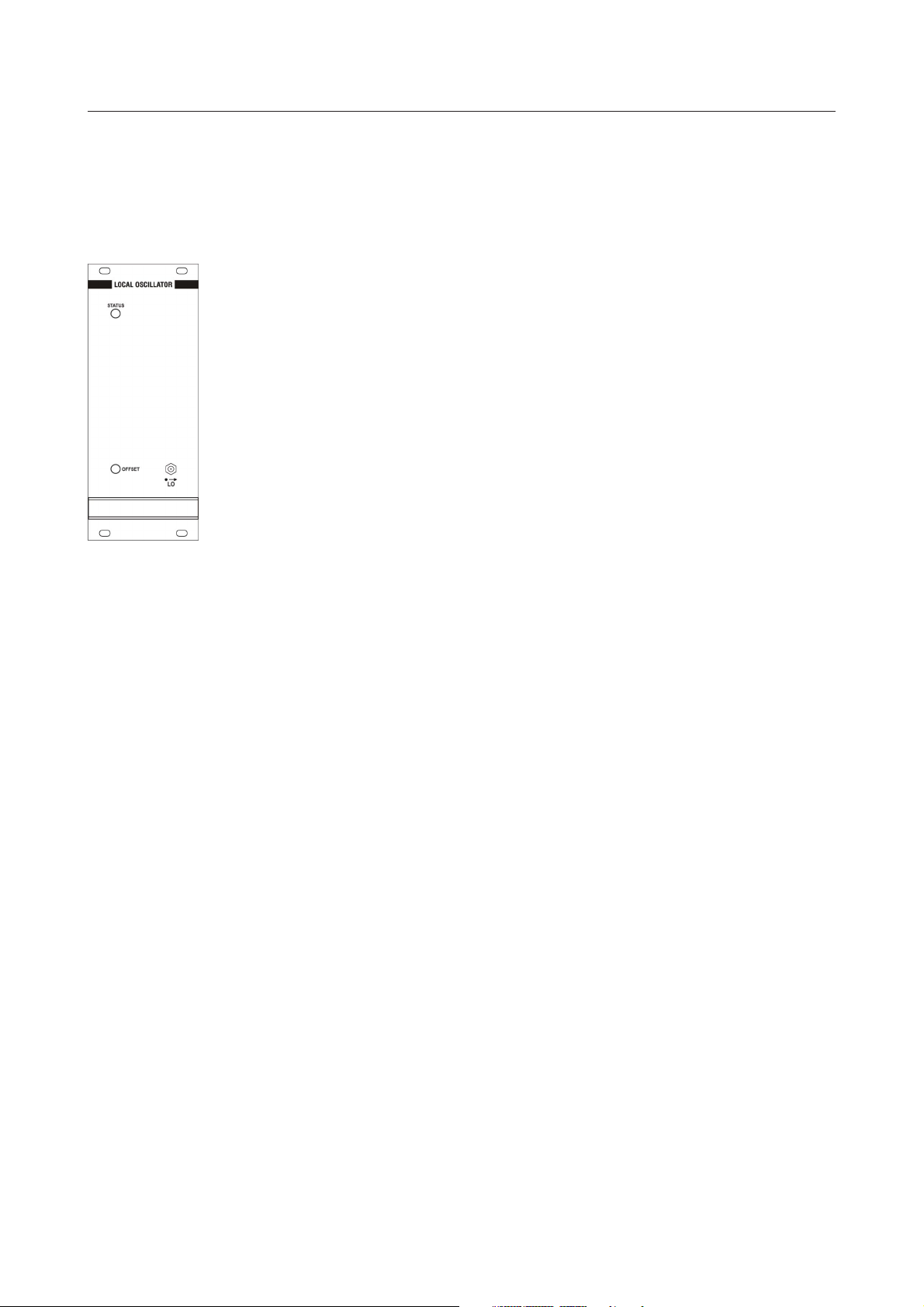
MULT. UHF LOCAL OSCILLATOR MODULE MTG0084AR0
DESCRIPTION
The synthesis system of the local oscillator for the channel conversion is based on a control
technique which allows to obtain the programming of the standard, the channel (split into
the three bands I, III, IV/V) and the line offset (as multiple of the line frequency of the
video signal) via software, with no change to be made.
The module includes an internal VCTCXO reference which can be locked to a more
precise 5/10MHz reference (trough the bus) needed if the field offset is used.
TECHNICAL CHARACTERISTICS
Nominal level +13dBm ±1dB
FM S/N ccir unweight. > 65dB
FM S/N ccir wght. > 60dB
Analog measures VCO control voltage
Carrier frequency synthesis A PLL
Offset Line offset, step ±1/12 line frequency
O.L. carrier characteristics On/Off selection and fine adjust
Frequency reference Internal TCXO externally lockable
External interface Microprocessor with RS485 protocol
Firmware Re-configurable via RS485
102
103

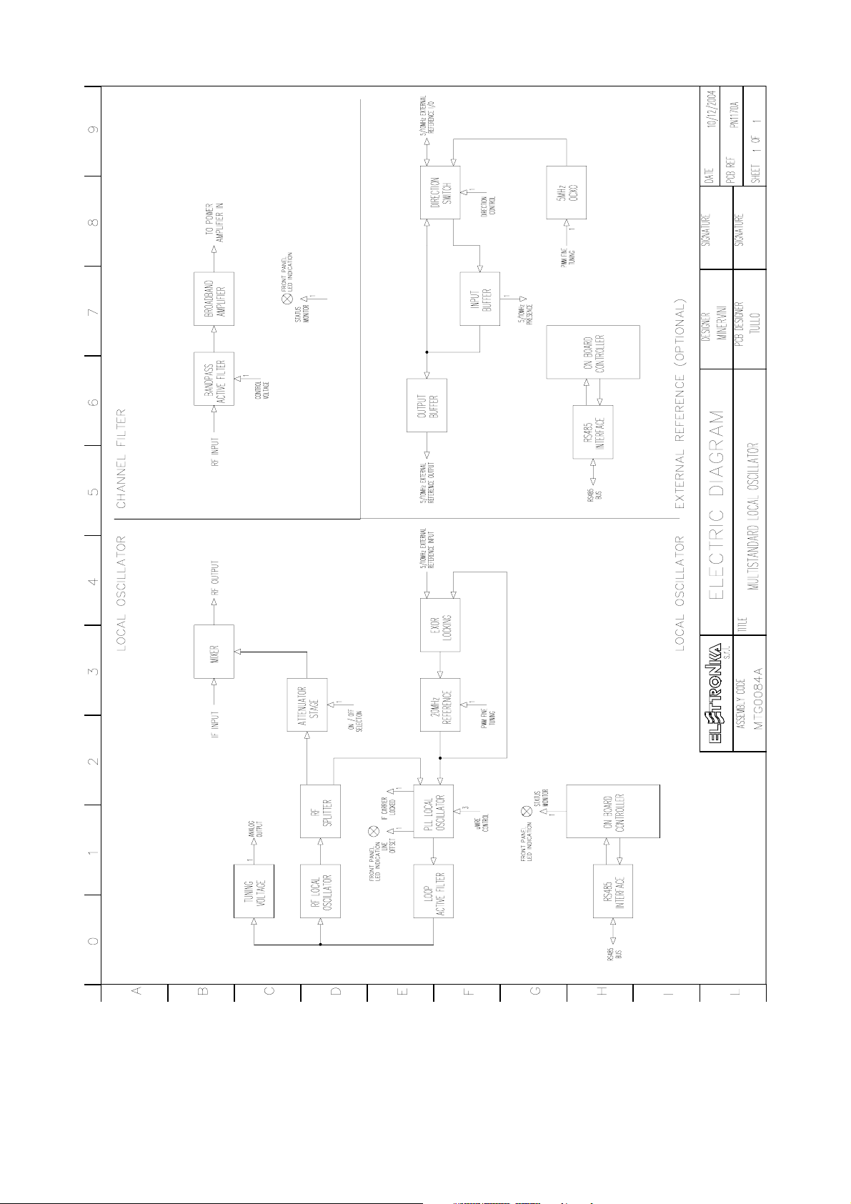
The module contains the following blocks:
1. Local oscillator generated the carrier to be synthesised, it is split into three windows (I-II / III / IV-V
band) to ensure the coverage of all of the TV channels to be implemented for all standards.
2. Radio-frequency splitter splits the signal coming from the local oscillator by means of splitters and
amplifiers, with 10dB attenuation and gain respectively, to ensure the complete isolation of the LO from
the other stages and to minimise the frequency pulling phenomenon.
3. PLL stage synthesises the desired channel by locking the LO to a 20MHz frequency reference by
means of a PLL which can be configured via uWire and provides the locking and line-offset indication
(LED on frontal panel); the choice is made via software.
4. Active ring filter stabilises the system in PLL retro-action and e has to be modified if the operating
band of the module changes (see table attached to the electrical diagram).
5. Conditioning stage of the correction voltage conditions the correction voltage of the PLL ring
providing a conditioned analog voltage for the A/D conversion; the voltage is processed by the
microcontroller of the display board (see MTG0079) to be displayed as VU-METER.
6. Mixer in the UPCONVERTER version of the module, converts to channel the intermediate frequency
coming from the pre-corrector (see MTG0073) using a LEVEL13 mixer (in case the module is only used
as LO, see REPEATER configuration, this stage is not present and the synthesised carrier goes directly to
the output of the module).
7. 20MHz reference the frequency reference to the PLL synthesis of the carrier is generated by an
internal TCXO which fine control of the frequency is internally generated via PWM by the microcontroller
or, alternately, can be locked to a more precise 5/10MHz external reference (see MTG0076).
8. Controller all of the described operations are managed by a microcontroller communicating to the user
interface board (see MTG0079) by RS485 protocol; the local controller stores the status of the module
and a reprogramming of the firmware (possible via RS485 from the display board) does not alter its
contents.
CALIBRATION PROCEDURE
- List of instrument
MEASURE INSTRUMENT
- Spectrum analyser
Lock of the carriers and reference
- Oscilloscope
- Tester
104
- Description of the adjustment points
COMPONENT DESCRIPTION
C1, C2, C3
J3
J5, J8
J4
JP1
J2
Tuning of the local oscillator (SCH0292 - 0309 - 0310)
LO input
RF link (absent in case of LO configuration)
LO monitor (panel)
Unused
Testpoint for the debug of the PLL
The calibration procedure of the module requires a complete structure of display board (see MTG0079)
and extension module (see MTG0095) in order to perform the software selection which will be referred
to later and power the module itself..
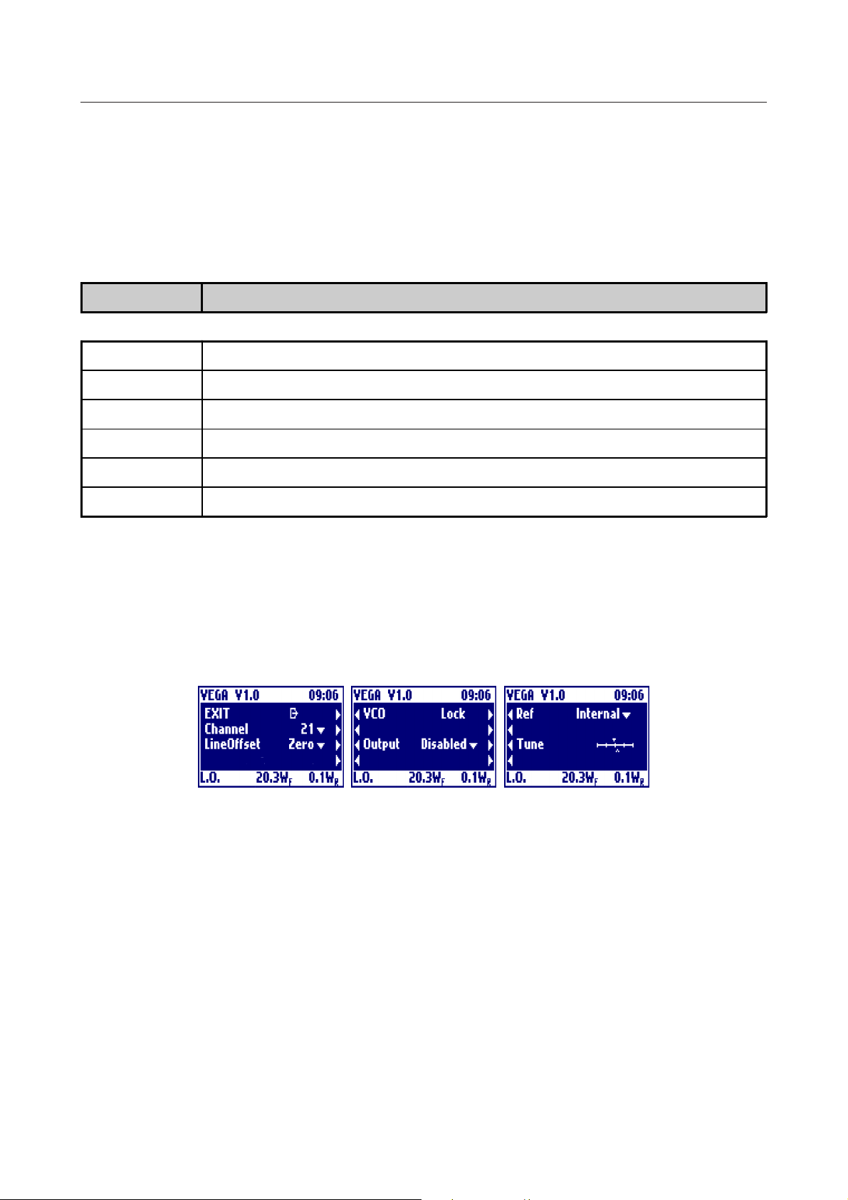
- Menu of the Multistandard UHF Local Oscillator Module
Verification of the local oscillator section connect a spectrum analyser to the monitor of the J4 module
and check the sections therein:
q Configure the module with Output Enabled, LineOffset Zero, Ref Internal and Channel on the
desired channel, and calibrate C1(C2 and C3) to lock the carrier to the LO frequency of the standard and
channel set (to change the standard refer to the standard changing procedure) and obtain a locking
voltage between 2V and 3V on TP1, checking that VCO is on Lock in the display menu.
Verification of the external reference section connect a spectrum analyser to the monitor of the J4
module and check the sections therein:
q Configure the module with Ref Internal and check that it is possible to find adjust the synthesised frequency
by acting on Tune.
105
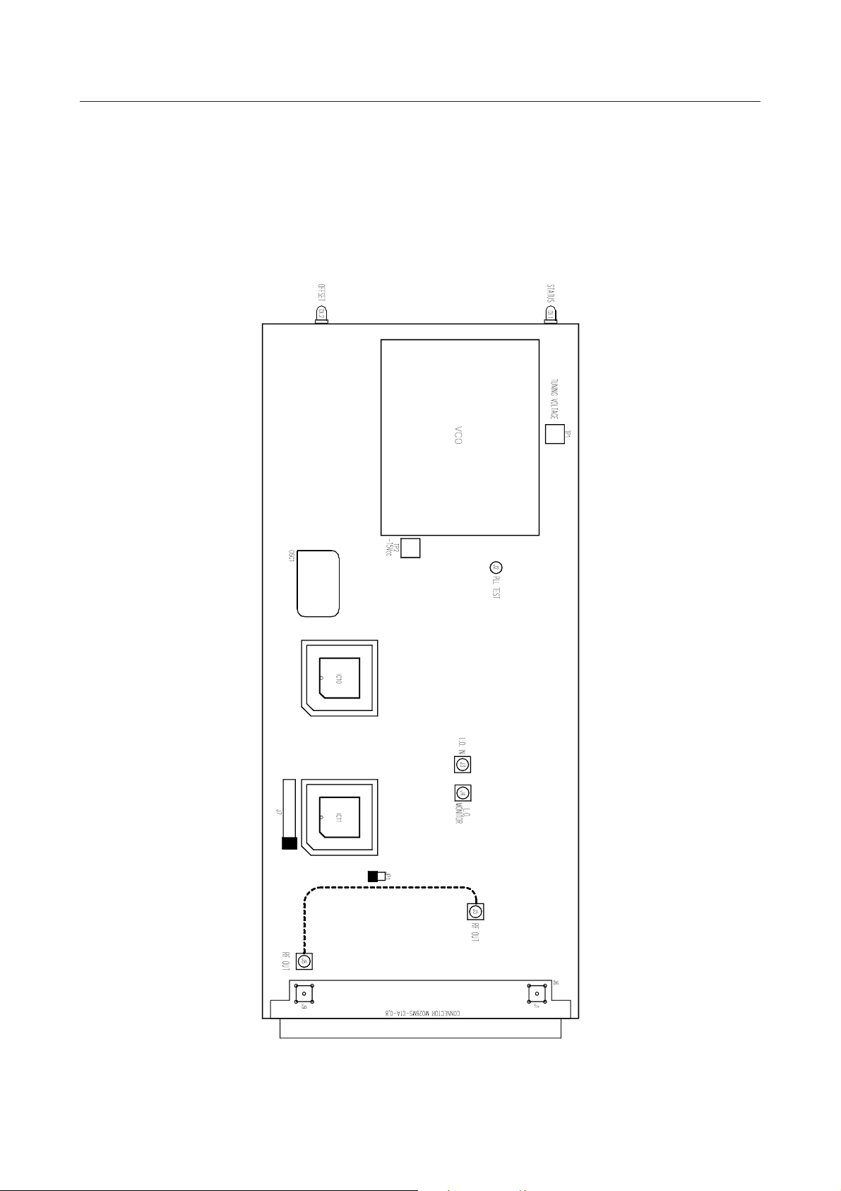
Component layout for adjustment points
106

Component layout SCH0293AR0
Component layout SCH0292AR0
107
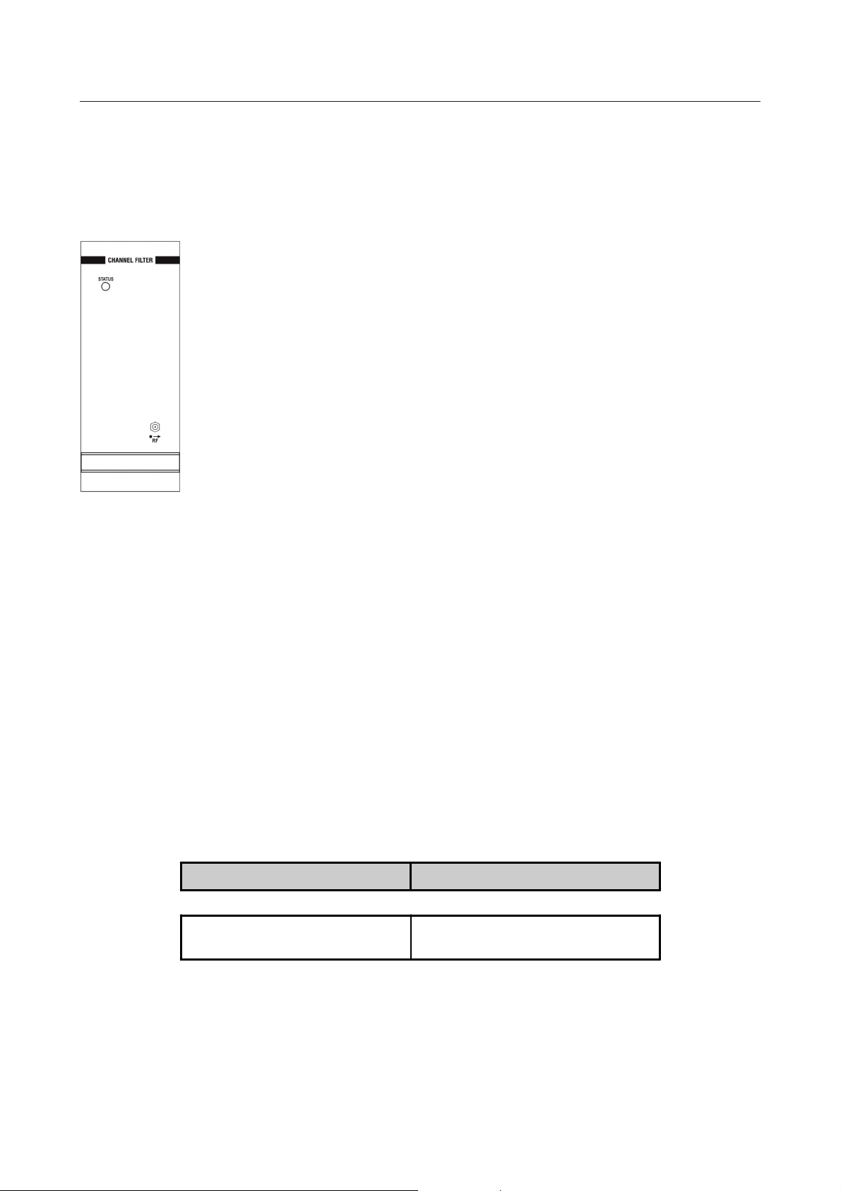
MULT. UHF CHANNEL FILTER MODULE MTG0075AR0
DESCRIPTION
The module filters the signal coming from the conversion mixer removing the local oscillator
and the upper side-band and contains the voltage-controlled gain stage composed by a
pin-diode attenuation cell followed by a wide-band amplification stage used as driver of
the final stage.
TECHNICAL CHARACTERISTICS
Input/output impedance 50W R.O.S.>20dB
Filter type Active 5-cell band-pass
RF-attenuation type 4 PIN-diodes cell
Output amplifier Wide band
Overall gain 25dB (max.)
The module contains the following blocks:
1. Active band-pass filter filters the lower side-band after conversion, it is split into three windows (I-II
/ III / IV-V band) to ensure the coverage of all of the TV channels to be implemented for all standards,
and contains the PIN-diode attenuation cell for the gain control.
2. Wide-band amplifier amplifies the filtered channel in order to obtain the correct driving level for the
RF final stages (see MTF0088-0087-0089).
CALIBRATION PROCEDURE
- List of instruments
MEASURE INSTRUMENT
Calibration of the channel filter
- Network analyser
- Spectrum analyser with tracking
108
- Description of the adjustment points
COMPONENT DESCRIPTION
C1-C8, C18-19
C17, C20-24,
C26-27, C31-32
L1-6
J6
JP1, R29
J2
J4
Channel filter calibration for bands III and IV-V
Channel filter calibration for band I-II
Channel filter calibration for band I-II
RF monitor (panel)
Local gain control of the filter
Channel filter input
Channel filter output
The calibration procedure of the module requires a complete structure of display board (see MTG0079)
and extension module (see MTG0095) in order to perform the software selection which will be referred
to later and power the module itself.
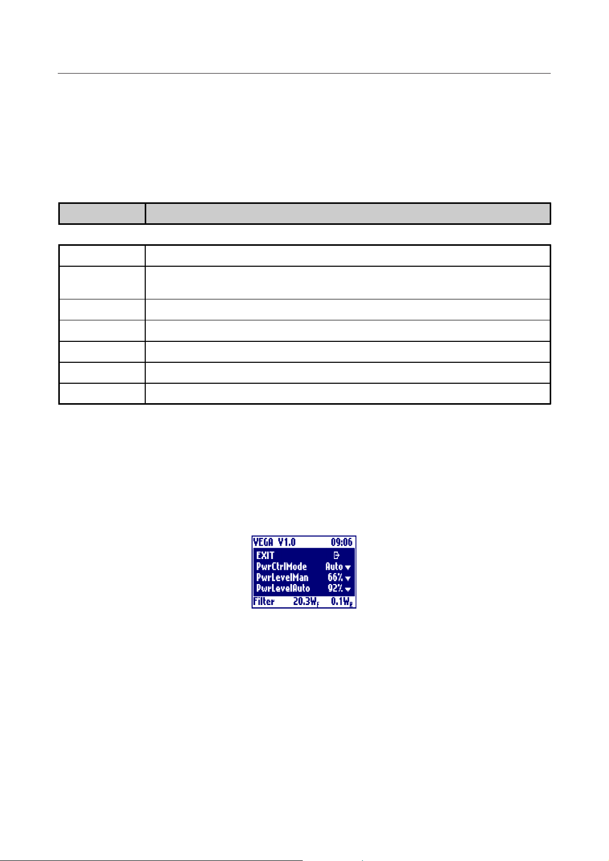
- Menu of the Multistandard UHF Channel Filter Module
Verification of the channel filter connect a network analyser to the channel filter and calibrate its
components to obtain the desired frequency response:
q Configure the module with PwrCtrlMode Man and verify that it is possible to change the gain of the filter
by acting on PwrLevelMan, setting JP1 Remote.
Verification of the wide-band amplifier section connect a spectrum analyser with tracking between J4
and J5 check that the frequency response of the amplifier is flat within 1dB from 50MHz to 900MHz.
109
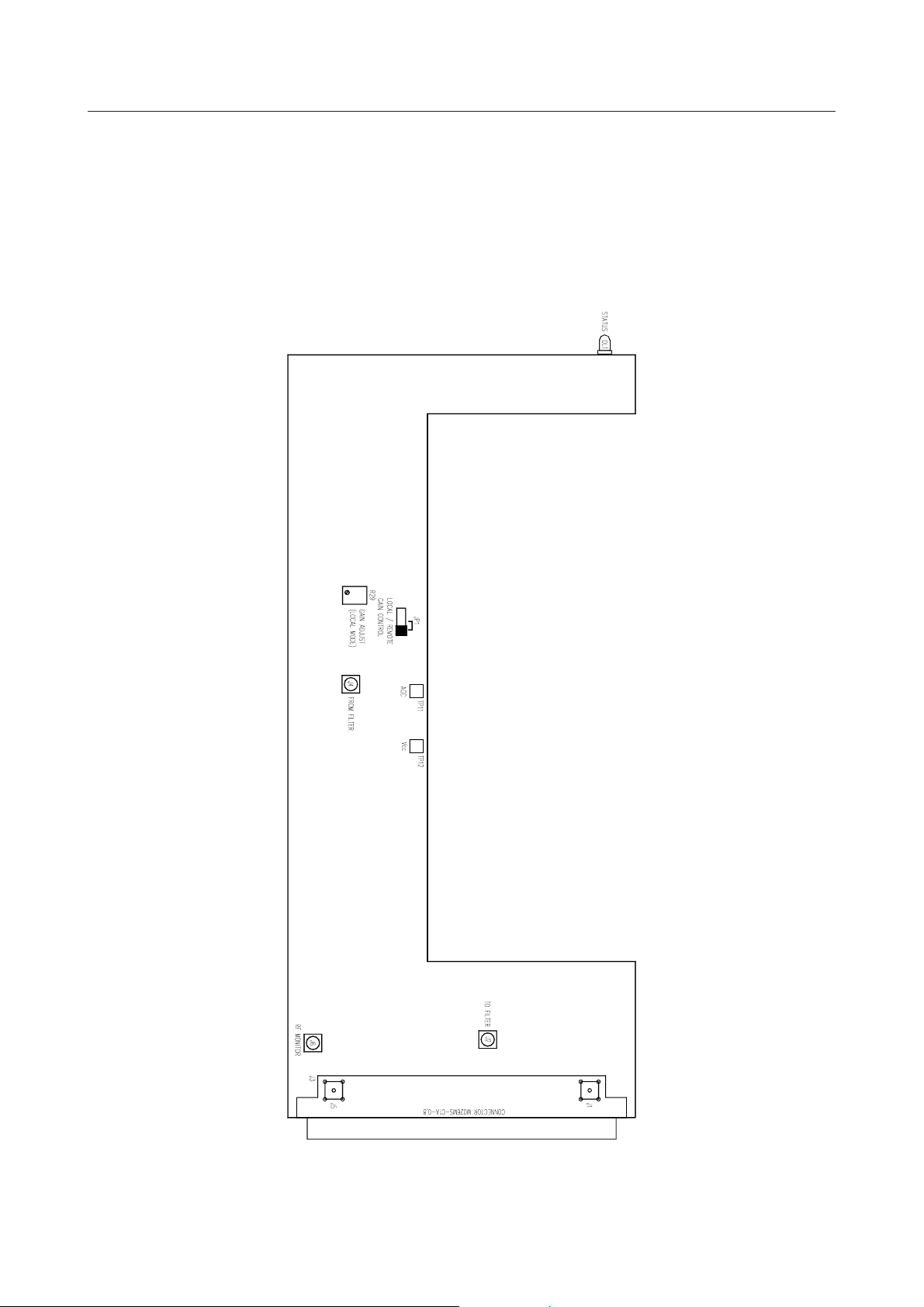
Component layout for adjustment points
110
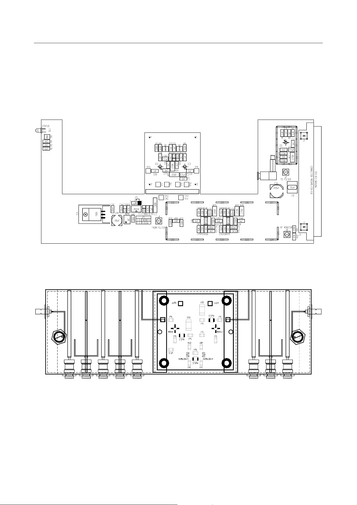
Component layout SCH0222AR2
Component layout UHF Channel Filter
111
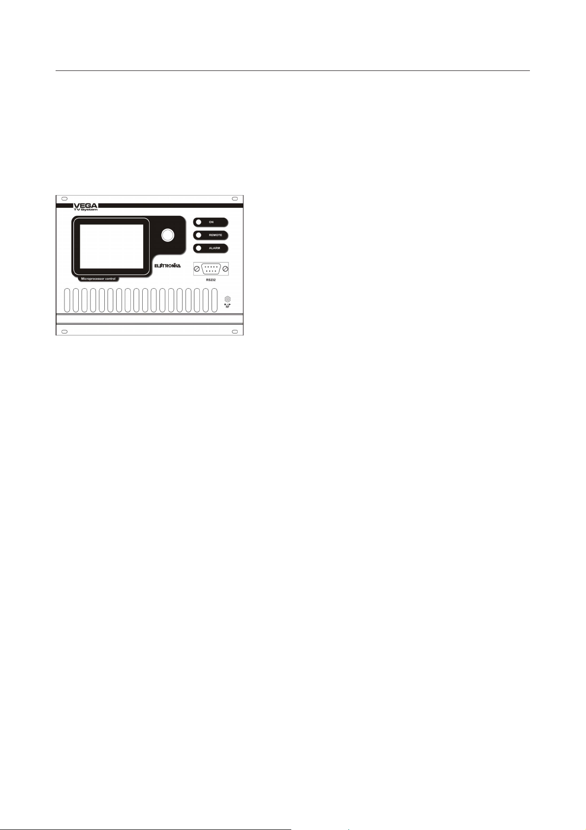
CONTROLLER MODULE MTG0079AR0
SCH0135AR1 DESCRIPTION
The Controller module, located on the right side of the VEGA
TV modulator, is the user interface of the whole modulator. It
gathers the data from all the sections of the modulator, processes
them by means of a 16bit flash micro-controller by Fujitsu and
makes them available to the user both through the local interface,
composed by a display and a knob, and the remote interface
made up by the serial port (either the RS232 on the front or the
RS485 on the back, as selected) or the interface of the
telemeasuring connector.
The acquisition and setting of all the concerned parameters is
made in two different ways. Analog measures reach the board
from the individual modules as voltages, are conditioned on the board and then converted by an internal A/D
converter in the micro.
The remaining parameters are gathered through a 2-wire RS485 interface, which runs on the bus. The display
board acts as master on this 485 bus. Besides it is provided with an RTC and a non-volatile memory on an
internal I2C bus.
- Dip-Switch
The display board is provided with 4 dip-switches. The dip-switches 3 and 4 are used to program the flash
memory of the flash micro-controller by Fujitsu, in detail:
DIP3: On DIP4: Off Boot Programming
DIP3: Off DIP4: On Run or Firmware Programming
The "Boot Programming" configuration is only for BIOS programming purposes.
Once the BIOS has been programmed, the firmware has to be programmed at least once in order to use the
board. The firmware programming and the normal operation of the board are obtained with the same position
of the dip switches.
For more detail on Firmware upgrade please refer to the "Firmware Upgrade" section.
DIP2: On Factory setting
DIP2 is set to ON only during the factory setup of the exciter. This allow to store in the memory all of the
settings made as 'factory defaults'.
Once the test is completed, and while the modulator is used normally, the DIP2 must be kept OFF.
112
 Loading...