

Page 1
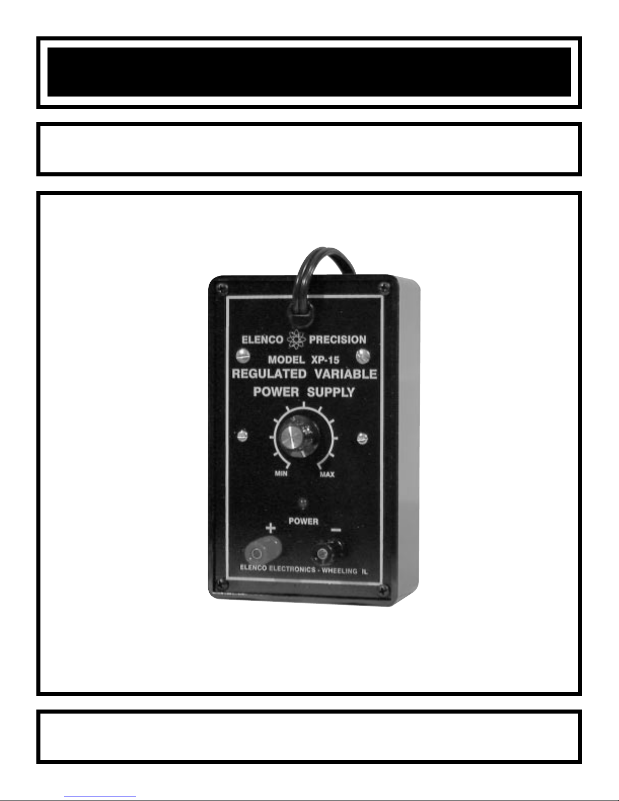
POWER SUPPLY KIT
MODEL XP-15K
Assembly and Instruction Manual
Page 2
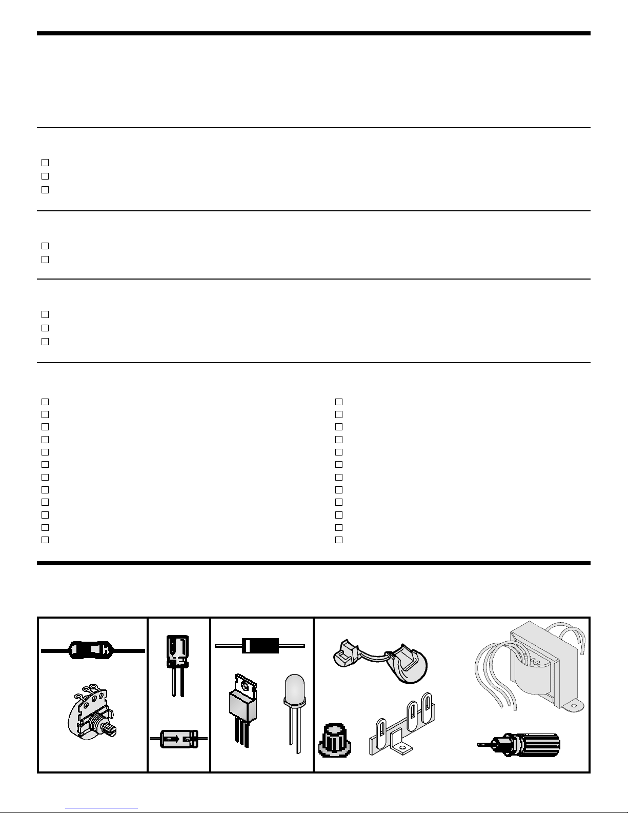
PARTS LIST
If any parts are missing or damaged, see instructor or bookstore. DO NOT contact your place of purchase as
they will not be able to help you.
Contact Elenco Electronics (address/phone/e-mail is at the back of this manual) for additional assistance, if
needed.
RESISTORS
Qty. Description Color Code Part #
1 130Ω 5% 1/4W brown-orange-brown-gold 131300
1 1.5kΩ 5% 1/4W brown-green-red-gold 141500
12kΩ Potentiometer 192422
CAPACITORS
Qty. Description Par t #
110µF 25V Electrolytic (axial) 271055
1 1,000µF 25V Electrolytic (radial) 291045
SEMICONDUCTORS
Qty. Description Par t #
2 1N4001 Diode 314001
1 LM-317 Regulator 330317
1 LED Red 350002
MISCELLANEOUS
-1-
Qty. Description Part #
1 T r ansformer YD-1485 440111
24” Solder 551124
1 Faceplate 614040
1 Knob 622009
1 Chassis Box 623240
1 Bushing 2 Wire 624002
1 Binding Post Black 625031
2 Nut Binding Post 625031HN
2 Lockwasher Binding Post 625031LW
1 Binding Post Red 625032
2 Screw 4-40 x 1/4” 641430
2 Screw 6-32 x 5/16” 641641
Qty. Description Part #
4 Screw #6 x 3/8” Self-tapping 643652
1 Nut 7mm 644101
2 Nut #4 644400
2 Nut #6 644600
1 Washer 8mm 645101
1 Lockwasher 5/16” 646101
2 Lockwasher #4 646401
2 Lockwasher #6 646600
1 Terminal Str ip 651003
10” 22 Ga. Red Wire 814220
1 Line Cord 2 Wire 862100
2” Shrink Tubing 890120
PARTS VERIFICA TION
Before beginning the assembly process, familiarize yourself with the components and this instruction book.
Verify that all of the parts are present. This is best done by checking off the parts in the par ts list.
Resistors Capacitor Semiconductors
Electrolytic
(radial)
Diode
2kΩ
Potentiometer
LM-317
Regulator
LED
Knob
T ransf ormer YD-1485
Electrolytic
(axial)
Binding Post with Nuts & Lockwasher
Miscellaneous
Bushing 2 Wire
Ter minal Str ip
Page 3
-2-
INTRODUCTION
Assembly of your XP-15 Regulated Variable P o w er Supply Kit will prove to be an exciting project and give much
satisfaction and personal achievement. If you have experience in soldering and wiring technique, you should
have no problem in the assembly of this kit. Care must be given to identifying the proper components and in
good soldering habits. Above all, take your time and follow the easy step-by-step instructions. Remember, “An
ounce of prevention is worth a pound of cure”. Avoid making mistakes and no problems will occur.
USE SAFETY GOGGLES WHEN ASSEMBLING THIS KIT!!
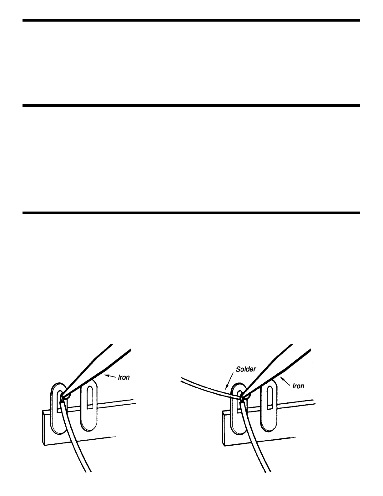
SOLDERING TECHNIQUES
The most important factor in assembling your power supply is good soldering techniques. Using the proper
soldering iron is of prime importance. A small pencil type iron of about 25-40 watts is recommended.The tip of
the iron should be kept clean at all times and well tinned (coated with a thin layer of molten solder). To keep the
tip clean, wipe it from time-to-time with a damp sponge. Size and care of the tip will eliminate problems. Use
only rosin core solder of 63/37 alloy. DO NOT USE ACID CORE SOLDER!!
Whenever possible, attach wire leads onto terminal lugs by forming tight mechanical connections before you
apply solder. For a good soldering job, heat the areas to be soldered sufficiently, so that the solder flows freely.
Position the soldering iron firmly against the wire lead and terminal. Apply the solder simultaneously to the
component lead or wire lead and to the terminal strip to be soldered so that good solder flow will occur. Remove
the solder feed when enough molten solder has been applied to form a thin coating on all metal parts in the
connection. After the solder feed has been removed, continue to heat the connection for an instant. This will
aid in the flow of the molten solder and insure against flux pockets. A properly soldered connection will have a
smooth bright finish. Do not blob the solder over the lead because this can result in a cold solder joint.
SPECIFICATIONS FOR XP-15 POWER SUPPLY
Output Voltage 1.25 - 15VDC
Output Current 0.5A @ 8V, 0.3A @ 12V, 0.2A @ 15V
Load Regulation 0.1V
Line Regulation 0.1V
Ripple Max. 0.01V RMS
Short Protection IC THERMO
Output Impedance 0.1 ohm
Page 4
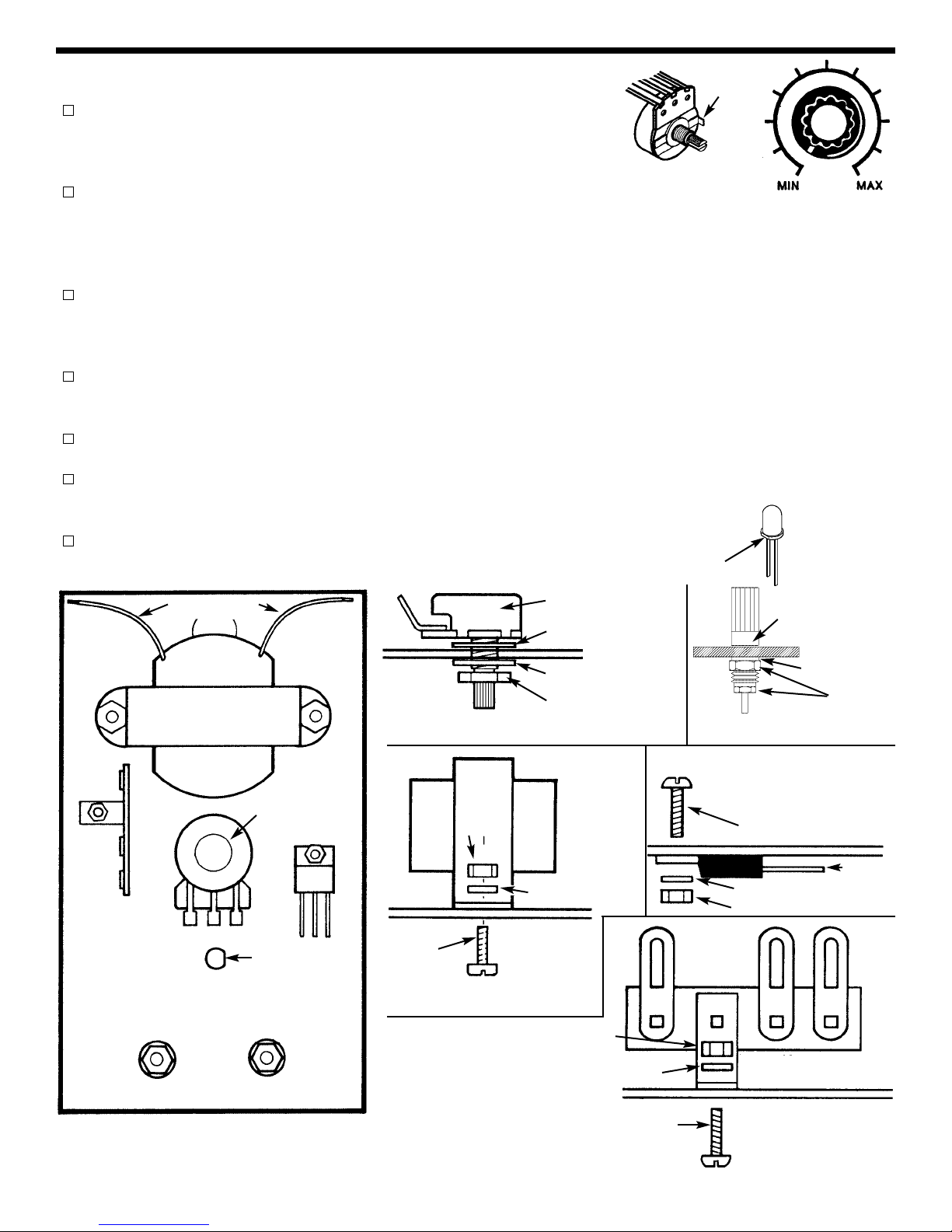
PANEL ASSEMBLY
Install the potentiometer with the lugs down as shown in Figure A.
Remove the tab as shown. Fasten in place with the parts as shown in
Figure B.
Turn the shafts on the pots fully counter-clockwise. Push the knobs onto the shafts so that
the line on the knob lines up with the end of the circle on the front panel as shown. If the knob is loose on
the pot shaft, insert a screwdriver in to the slot and expand the slot slightly. If the knob has a set screw,
tighten the set screw located on the side of the knob.
Install the binding posts with the colors in the order as shown in Figure A. Remove the large nut and the
lockwasher. Inser t the post into the hole and fasten it with the nut and lockwasher (see Figure C). Tighten
down the nut with pliers.
Install the transformer with the black wires as shown in Figure A. Use a 6-32 x 5/16” screw , a #6 lockwasher
and a #6 nut on each side to fasten in place as shown in Figure D.
Install the LM-317 IC as shown in Figure A. Use the par ts as shown in Figure E.
Install the terminal strip as shown in Figure A. Use a 4-40 x 1/4” screw and a #4 nut and #4 lockwasher as
shown in Figure F.
Install the LED. Push the LED in place with the flat side as shown in Figure A.
-3-
Lockwasher
Nuts
Plastic Washer
Figure C
Figure A
Figure B
Black Wires
Transformer
Terminal
Strip
Figure D
Flat
Side
LED
Binding
Posts
Black
Red
LM317 IC
Potentiometer
#6 Lockwasher
#6 Nut
6-32 x 5/16”
Screw
Figure E
Figure F
4-40 x 1/4” Screw
#4 Lockwasher
#4 Nut
#4 Lockwasher
#4 Nut
LM317
IC
4-40 x 1/4” screw
Potentiometer
5/16” Lockwasher
8mm Washer
7mm Nut
Flat
Remove
Tab
Page 5
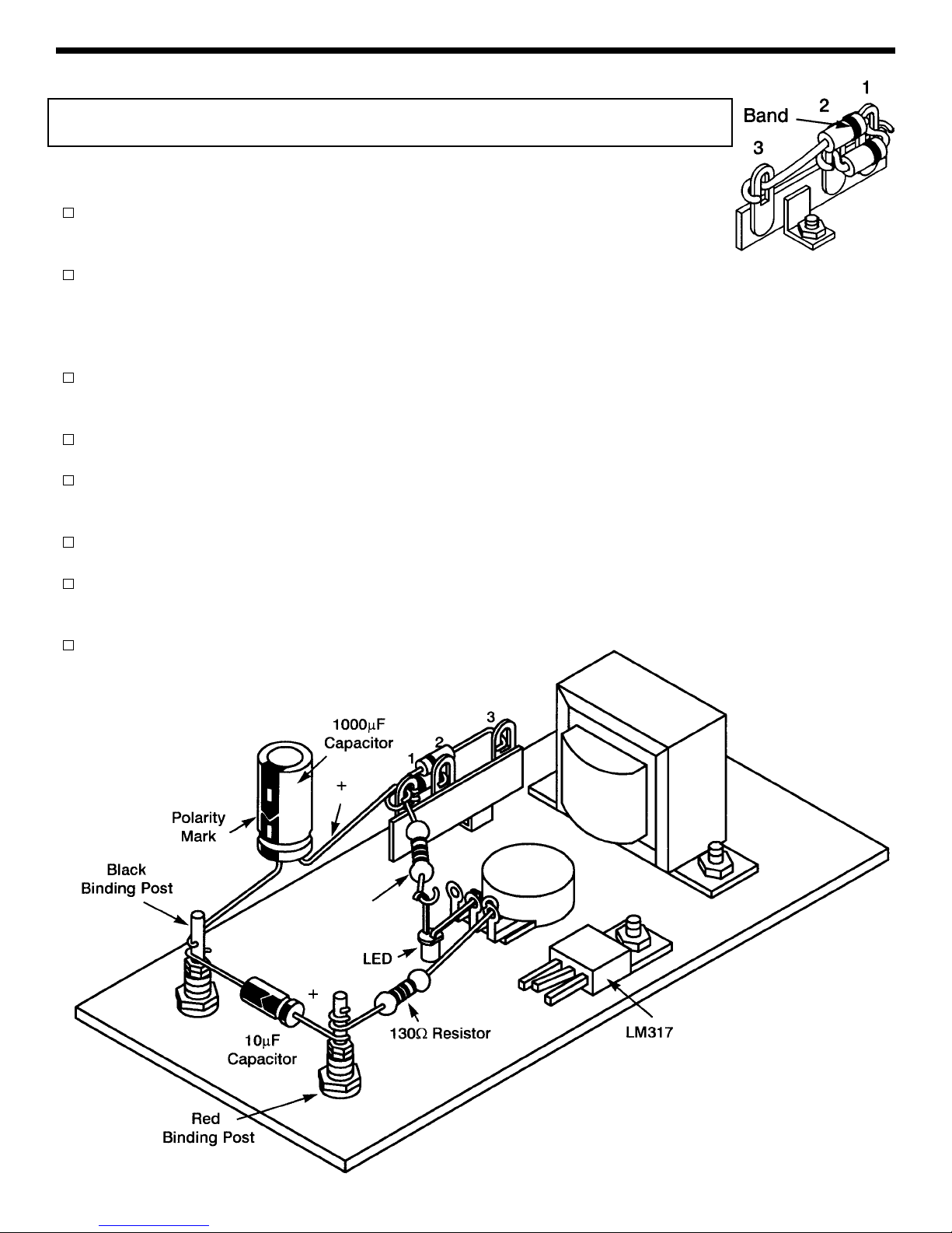
COMPONENT ASSEMBLY
Note: When you are instructed to “fasten” a lead to a lug, mak e a connection, but do not
solder until later.
Install the following components as shown in Figure G.
Fasten the banded end of a 1N4001 diode to terminal 1 of the terminal strip. Fasten
the other end to terminal 2.
Fasten the banded end of the other 1N4001 diode to terminal 1 of the terminal strip. Fasten the other
end
to terminal 3. Note: Make sure that the diode lead on terminal 1 or 3 doesn’t shor t to terminal 2.
Install the following components as shown in Figure H.
Fasten one end of the 1.5kΩ resistor (brown-green-red-gold) to terminal 1 of the terminal strip. Solder one
end to the LED lead.
Fasten the flat side lead of the LED to the middle lug of the 2kΩ pot.
Fasten the positive lead of the 1000µF capacitor to terminal 1 of the terminal str ip. Be sure that the polarity
is as shown in Figure H.
Fasten the negative lead of the 1000µF capacitor to the black binding post.
Fasten the negativ e lead of the 10µF capacitor to the blac k binding post. Be sure that the polarity is as shown
in Figure H. Fasten the positive lead to the red binding post.
Fasten one end of the 130Ω resistor (brown-
orange-brown-gold) to the red binding post.
Fasten the other end to the right lug
of the potentiometer.
-4-
Figure G
Figure H
1.5kΩ Resistor
2kΩ Pot
Page 6
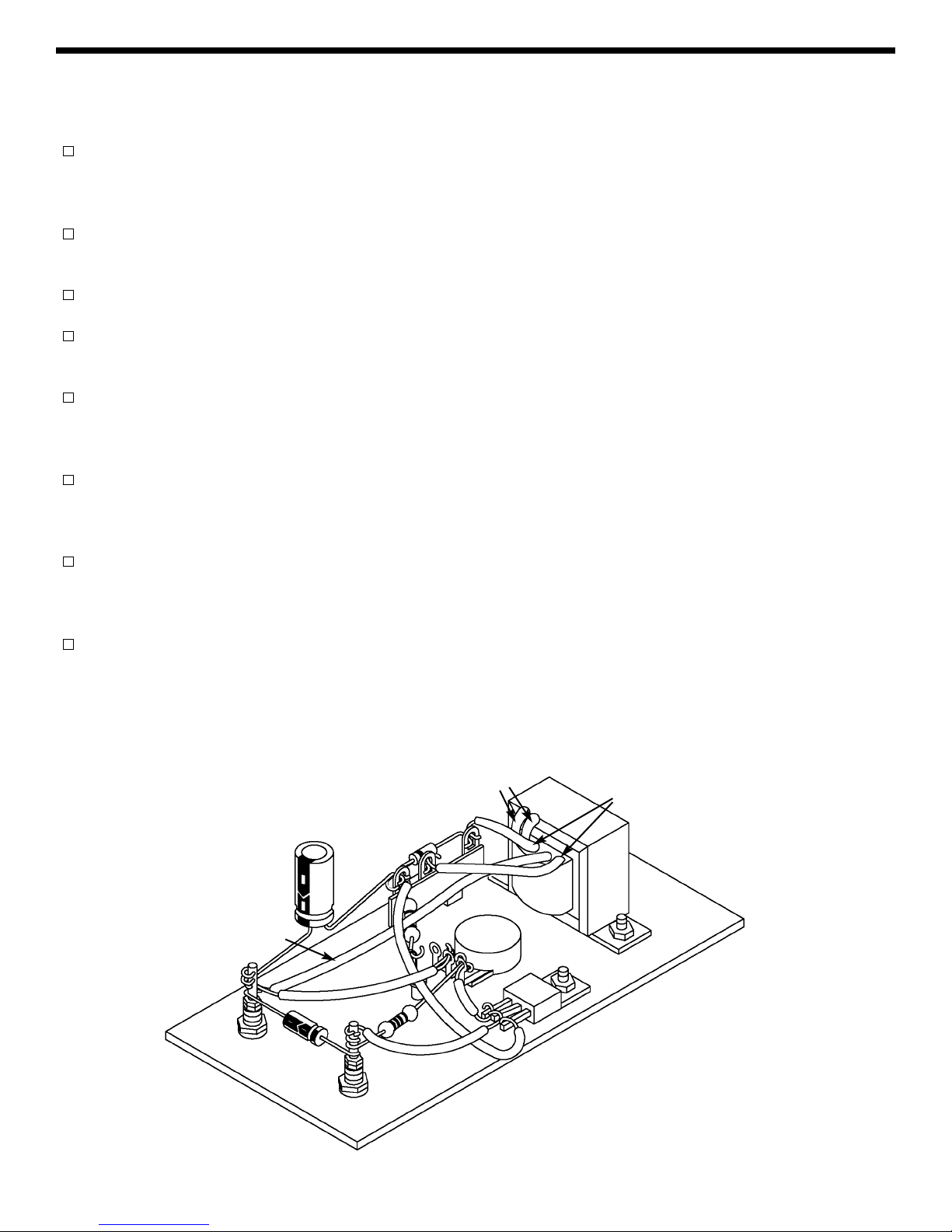
WIRING
Install the following wires as shown in Figure I.
Cut both yellow transf ormer wire so that they are 3”. Strip 1/4”insulation off the end. Solder one of the yellow
wires from the transformer to terminal 3 on the terminal strip (when soldered, there should be one wire and
one diode on the terminal).
Solder the other yellow wire from the transformer to terminal 2 on the ter minal strip (when soldered, there
should be one wire and one diode on the terminal).
Fasten the blue wire from the transformer to the black binding post.
The red wires on the transformer are not used. To keep them from shorting to other components, cut them
off close to the transformer.
Cut a 2” piece of wire and strip 1/4” of insulation off both ends. Solder one end to the center lug of the
potentiometer (when soldered, there should be one LED lead and one wire on the lug). Solder the other end
to the black binding post (when soldered, there should be two wires and two capacitors on the lug).
Cut a 2” piece of wire and strip 1/4” of insulation off both ends. Solder one end to the right lug of the
potentiometer (when soldered, there should be one wire and one resistor on the lug). Solder the other end
to the left lead of the LM317 IC.
Cut a 2” piece of wire and strip 1/4” of insulation off of both ends. Solder one end to the red binding post
(when soldered, there should be a wire, a resistor and a capacitor on the shaft). Bend up the center lug of
the LM317 IC slightly. Solder the other end of the wire to the center lead of the LM317 IC.
Cut a 4”piece of wire and strip 1/4” of insulation off of both ends. Solder one end to terminal 1 of the terminal
strip (when soldered, there should be 2 diode leads, 1 resistor lead, 1 capacitor lead and 1 wire on the
terminal). Solder the other end of the wire to the right lead of the LM317 IC.
-5-
Red Post
Black Post
Blue Wire
Red Wires
Yellow Wires
1
2
3
Figure I
Page 7
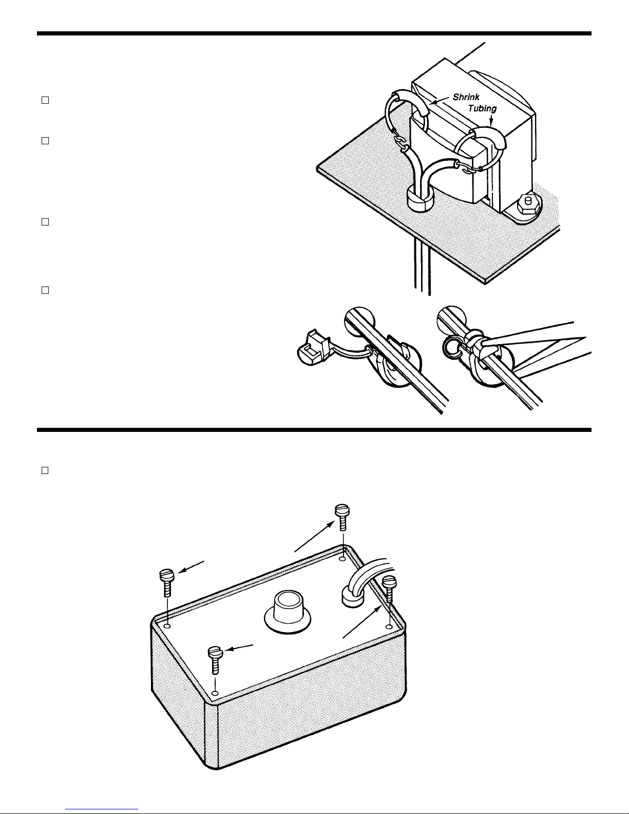
LINE CORD ASSEMBLY
Install the following wires as shown in Figure J.
Cut the two black wires from the transformer to
1 1/2”. Strip 1/4” of insulation off of each wire.
Feed 2 inches of line cord into the hole of the
chassis. Place the line cord in the slot of the
strain relief and squeeze the two sections
together with pliers. Then, insert the strain
relief into the hole.
Separate the two line cord wires. Place 1” of
shrink tubing over each blac k transformer wire.
Solder the line cord wires to the black
transformer wires as shown in the figure.
Slide the shrink tubing up to cover the solder
joints. Shrink the tubing with the heat from
your soldering iron. BE CAREFUL NOT TO
TOUCH THE SHRINK TUBING OR WIRES
WITH THE IRON.
FINAL ASSEMBLY
Place the power supply panel in the case and fasten with four #6 x 3/8” self-tapping screws as shown in
Figure K.
Figure K
Figure J
-6-
#6 x 3/8” Screw
#6 x 3/8” Screw
Page 8
-7-
TESTING THE XP-15 POWER SUPPLY
Testing the XP-15K Power Supply is v ery simple. Before applying pow er to the unit, be sure that all of the wiring
and soldering is firm. If so, obtain a digital voltmeter. Apply power to the XP-15K and vary the voltage control
knob.
Next, short the output of the supply. It should turn off and recover when the short is removed. If you have a
2.5Ω 1 watt resistor, set the voltage to 1.25 volts and place is across the output terminals (a 1/2 watt will work,
but use it only a few seconds). The output of the supply should not change more than 0.1 volts. Set the output
voltage to 15 volts and place a 75Ω 5 watt resistor across the output terminals. Again, the output should not
change by more than 0.1 volts. In making these tests, the voltmeter leads should be clipped directly to the
output terminals and not to the load leads. This is to prevent errors due to voltage drop in the load leads.
Should any of these tests fail, refer to the troubleshooting guide.
CIRCUIT DESCRIPTION
INTRODUCTION
The XP-15K Power Supply features an output voltage variable from 1.25 to 15V at 0.5 ampere maximum
current. The voltage is regulated to within 0.1V when going from zero load to full load. Varying the input AC
voltage from 110 to 130V will have practically no effect on the output voltage. This is because of the specially
designed IC circuit used in the XP-15K. Severe overloading or even short circuiting the output will not damage
the supply. Special turn-off circuits in the IC sense the overload and turn off the output.
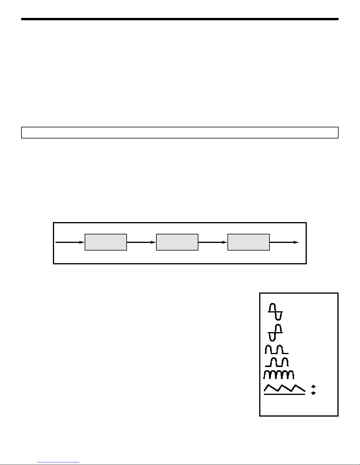
Figure 1 shows a simplified circuit diagram of the power supply. It consists of a power transformer , a DC rectifier
stage and the regulator stage.
TRANSFORMER
The transformer T1 serves two purposes. First, it reduces the 120VAC input to
18VAC to allow the proper voltage to enter the rectifier stage. Second, it isolates
the power supply output from the 120VAC line. This prevents the user from
dangerous voltage shock should they be standing in a grounded area.
AC to DC CONVERTER
The AC to DC converter consists of diodes D1 and D2 and capacitor C1.
Transformer T1 has two secondary windings which are 180 degrees out of phase.
The AC output of each winding is shown in Figure 2A and 2B.
Diodes are semiconductor devices that allow current to flow in one direction. The
arrow in Figure 3 points to the direction that the current will flow. Only when the
transformer voltage is positiv e will current flo w through the diodes . Figure 3 shows
the simplest possible rectifier circuit. This circuit is known as a half wave rectifier.
Here, the diode conducts only half the time when the AC wa v e is positiv e as sho wn
in 2C. Use of this circuit is simple but inefficient. The big gap between cycles
requires much more filtering to obtain a smooth DC voltage.
Figure 1
Simplified diagram of positive power supply
120VAC
Input
18VAC 20VDC 1.25 - 15V
Regulated
Output
Transformer
120V to 18V
AC to DC
Converter
Voltage
Regulator
Figure 2
Voltage Waveform for Supply
A) Transformer
Winding AB
B) Transformer
Winding BC
C) Output of
diode D1.
D) Output of
diode D2.
E) Total of diodes
D1 & D2.
20V
F) Output of capacitor C1
Ripple depends on load
current (expanded).
Page 9

-8-
By the addition of a second diode and transformer winding, we can fill
in the gap between cycles as shown in Figure 4. This circuit is called
full wave rectification. Each diode conducts when the voltage is
positive. By adding the two outputs, the voltage presented to capacitor
C1 is more complete, thus, easier to filter , as shown in Figure 2E. When
used in 60 cycles AC input power, the output of a full wave rectifier will
be 120 cycles.
Capacitor C1 is used to store the current charges, thus smoothing the
DC voltage. The larger the capacitor, the more current is stored. In this
design, a 1000µF capacitor is used, which allows about 2 volts of AC
ripple when one half amp is drawn.
In practice, the current through the diodes is not as shown in Figure 2C .
Because capacitor C1 has a charge after the first cycle, the diode will
not conduct until the positive AC voltage exceeds the positive voltage in
the capacitor. Figure 5 shows a better picture of what the current flow
looks like, assuming no loss in the diode.
It takes a few cycles for the voltage to build up on the capacitor. This depends on the resistance of the winding
and diode. After the initial start-up, there will be a charge and discharge on the capacitor depending on the
current drawn by the output load. Remember, current only flows through the diode when the anode is more
positive than the cathode. Thus, current will flow in short bursts as shown in Figure 5C.
The DC load current may be one ampere, but the peak diode current may be three times that. Therefore, the
diode rating must be sufficient to handle the peak current. The 1N4001 has a peak current rating of 10 amps.
REGULATOR CIRCUIT
The regulator circuit in the Model XP-15K Power Supply consists of a LM-317
integrated circuit. This IC is specially designed to perform the regulation
function. Figure 6 shows a simplified circuit of how the LM317 IC works.
Transistors Q1 and Q2 form a circuit known as a differential amplifier . Transistor
Q1’s base is connected to a stable 1.5V reference voltage. The base of Q2 is
connected to the regulator output circuit through a voltage divider network. The
collector of transistor Q2 is connected to a current source. This basically is a
PNP transistor biased to draw about 1mA current. Transistor Q2 sees the
current source as a very high resistor of about 1 meg ohms. Thus, the gain of
transistor Q2 is very high.
Transistor Q5 is called the pass transistor. It controls the current reaching the output. Transistors Q3 and Q4 are
emitter followers . Their function is to raise the impedance of the pass transistor . Note that transistor Q2, Q3, Q4,
Q5 and resistor R1 form a closed loop. Also, note that the feedback to the base of Q2 is negative, that is, the
output at emitter Q5 goes negative. Now, if the 1.25V output voltage goes down because of current drain at the
output, the base of Q2 will drop, f orcing the collector voltage of Q2 to go higher. This will bring the output voltage
back to 1.25V. This is the basis of all negative feedback regulators.
Another feature of the LM-317 regulator is to protect the IC against overload
and output shorts. If the IC is overloaded, the junction will overheat. A
transistor will sense this overheating and shut down transistor Q5.
The LM-317 IC is basically a 1.25V regulator. To be able to vary the output
1.25 - 15V, we stack the IC on a DC voltage as shown in Figure 6a. When
VR1 equals zero, the output voltage is 1.25V as determined by the LM-317
IC. Note that the voltage across VR1 will equal the 1.25 volts across R1,
therefore, the output voltage will be 2.5 volts. When VR1 is 5 times R1, the
output voltage is
7.5V. As you can see, varying resistor VR1 will vary the
voltage from 1.25V to 15V.
Figure 5
A) Transformer
Winding
B) Voltage C1
C) Current
through diodes
20V
Peak
20V
Figure 4
Full Wav e Rectifier
Figure 3
Half Wav e Rectifier
Figure 6
2V
Output
R1
R2
Divider
Q1
Q2
1.5V
Q3
Q4
Q5
Current
Source
Equalized
to 1 Meg.
Figure 6a
1.25 - 15V
R1
VR1
LM-317
Page 10

-9-
TROUBLESHOOTING GUIDE
Consult your instructor or contact Elenco Electronics if you have any problems. DO NOT contact your place of
purchase as they will not be able to help you.
LED Not Lit
1) Check transformer and line cord.
2) Check for 20VDC at the cathode of D1.
3) LED in backwards or defective.
No Output Voltage
1) Check AC voltage across points A & B or B & C. It should read about 18VAC.
2) Measure voltage at the output of D1. It should read about 20 volts. If not, then check D1, D2 and C1.
Poor Regulation
1) Check AC ripple at the input of the regulator. It should be less than 2.5V.
2) If ripple is greater, check diodes and the filter of capacitor C1.
QUIZ
1.
AC voltage is supplied to the rectifier stages by the . . .
A. step up transformer.
B. step down transformer.
C. 1 to 1 transformer.
D. AC to DC transformer.
2.The secondar y windings of the transformer are . . .
A. 90Oout of phase.
B. 180Oout of phase.
C. 270Oout of phase.
D. 320Oout of phase.
3. Diodes allow current to flow . . .
A. when the anode is more negative than the
cathode.
B. when the cathode is more positive than the
anode.
C. in one direction.
D. when a negative or positive voltage is on the
anode.
4.
What circuit is more efficient for rectifying AC to DC?
A. Hartley oscillator.
B. Half-walf.
C. Schmitt trigger.
D. Full wave.
5.The DC voltage is smoothed by using a . . .
A. half-wave rectification circuit.
B. small value capacitor with a high voltage
value.
C. Large value capacitor.
D. 90
O
out of phase rectification circuit.
Answers: 1. B, 2. B, 3. C, 4. D, 5.C, 6. D, 7.D, 8. C, 9.D, 10. A
6. An inefficient rectification circuit usually contains . . .
A. large gaps between cycles.
B. twice the AC voltage needed.
C. more diodes.
D. all of the above.
7.The maximum current that a diode can handle is
determined by . . .
A. the transformer’s current rating.
B. the amount of AC ripple.
C. three times the diode rating.
D. peak current rating.
8.The LM-317 will shut down when . . .
A. the output voltage is too high.
B. no current is being drawn.
C. the junction overheats.
D. the output voltage drops to 1.25V.
9.
The LM-317 regulator contains . . .
A. a pass transistor.
B. a constant current source.
C. a differential amplifier.
D. all of the above.
10.The LM-317 is basically . . .
A. a 1.25V regulator.
B. a 6.25V regulator.
C. a 2.5V regulator.
D. a negative voltage regulator.
Page 11
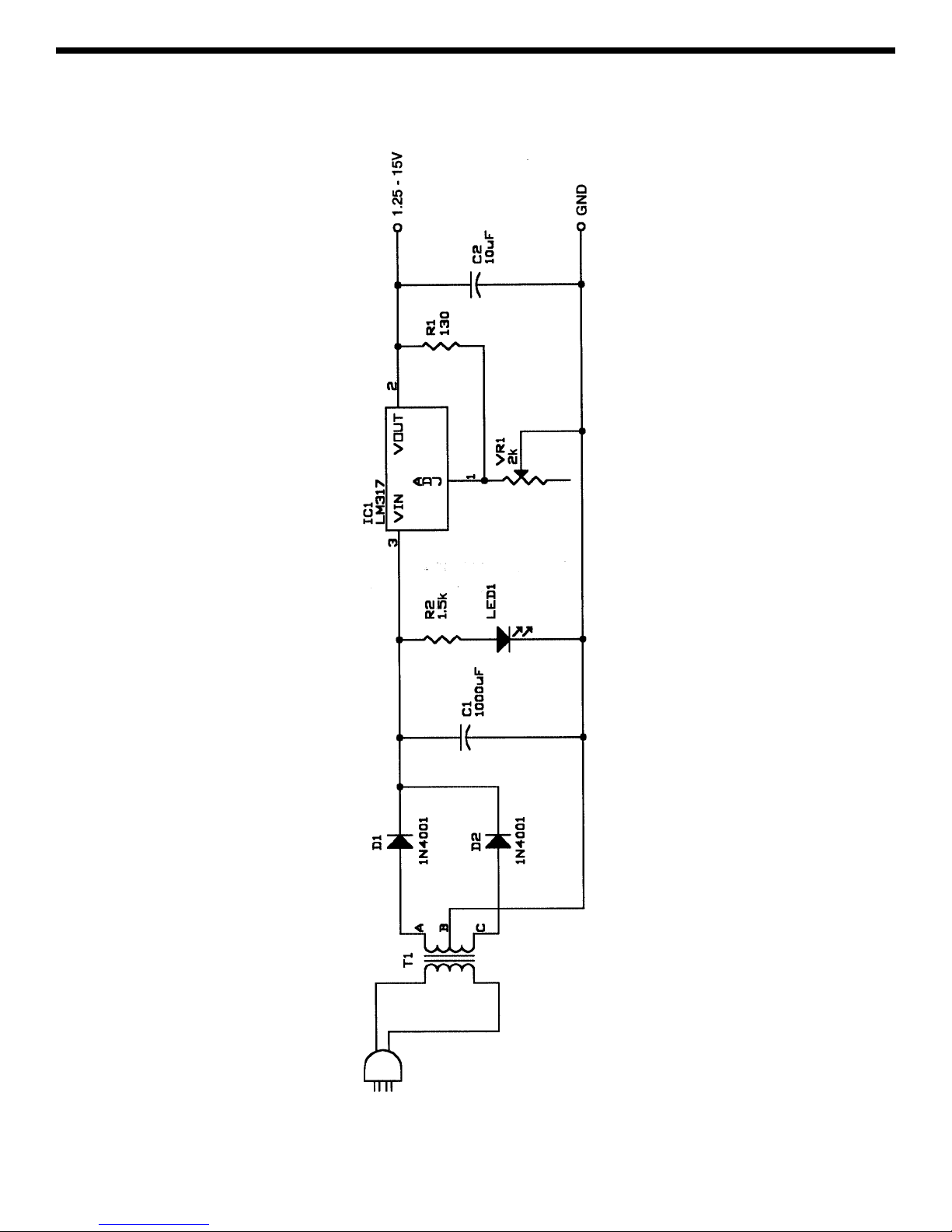
SCHEMATIC DIAGRAM
-10-
Page 12

 Loading...